EP3505992A1 - Display device having an eyepiece - Google Patents
Display device having an eyepiece Download PDFInfo
- Publication number
- EP3505992A1 EP3505992A1 EP18212953.6A EP18212953A EP3505992A1 EP 3505992 A1 EP3505992 A1 EP 3505992A1 EP 18212953 A EP18212953 A EP 18212953A EP 3505992 A1 EP3505992 A1 EP 3505992A1
- Authority
- EP
- European Patent Office
- Prior art keywords
- display device
- wave plate
- display panel
- light
- quarter
- Prior art date
- Legal status (The legal status is an assumption and is not a legal conclusion. Google has not performed a legal analysis and makes no representation as to the accuracy of the status listed.)
- Granted
Links
Images







Classifications
-
- G—PHYSICS
- G02—OPTICS
- G02B—OPTICAL ELEMENTS, SYSTEMS OR APPARATUS
- G02B5/00—Optical elements other than lenses
- G02B5/30—Polarising elements
-
- G—PHYSICS
- G02—OPTICS
- G02B—OPTICAL ELEMENTS, SYSTEMS OR APPARATUS
- G02B25/00—Eyepieces; Magnifying glasses
- G02B25/001—Eyepieces
-
- G—PHYSICS
- G02—OPTICS
- G02B—OPTICAL ELEMENTS, SYSTEMS OR APPARATUS
- G02B27/00—Optical systems or apparatus not provided for by any of the groups G02B1/00 - G02B26/00, G02B30/00
- G02B27/01—Head-up displays
- G02B27/017—Head mounted
- G02B27/0172—Head mounted characterised by optical features
-
- G—PHYSICS
- G02—OPTICS
- G02B—OPTICAL ELEMENTS, SYSTEMS OR APPARATUS
- G02B27/00—Optical systems or apparatus not provided for by any of the groups G02B1/00 - G02B26/00, G02B30/00
- G02B27/02—Viewing or reading apparatus
- G02B27/022—Viewing apparatus
-
- G—PHYSICS
- G02—OPTICS
- G02B—OPTICAL ELEMENTS, SYSTEMS OR APPARATUS
- G02B27/00—Optical systems or apparatus not provided for by any of the groups G02B1/00 - G02B26/00, G02B30/00
- G02B27/28—Optical systems or apparatus not provided for by any of the groups G02B1/00 - G02B26/00, G02B30/00 for polarising
-
- G—PHYSICS
- G02—OPTICS
- G02B—OPTICAL ELEMENTS, SYSTEMS OR APPARATUS
- G02B27/00—Optical systems or apparatus not provided for by any of the groups G02B1/00 - G02B26/00, G02B30/00
- G02B27/28—Optical systems or apparatus not provided for by any of the groups G02B1/00 - G02B26/00, G02B30/00 for polarising
- G02B27/286—Optical systems or apparatus not provided for by any of the groups G02B1/00 - G02B26/00, G02B30/00 for polarising for controlling or changing the state of polarisation, e.g. transforming one polarisation state into another
-
- G—PHYSICS
- G02—OPTICS
- G02B—OPTICAL ELEMENTS, SYSTEMS OR APPARATUS
- G02B5/00—Optical elements other than lenses
- G02B5/20—Filters
- G02B5/22—Absorbing filters
-
- G—PHYSICS
- G02—OPTICS
- G02B—OPTICAL ELEMENTS, SYSTEMS OR APPARATUS
- G02B5/00—Optical elements other than lenses
- G02B5/30—Polarising elements
- G02B5/3025—Polarisers, i.e. arrangements capable of producing a definite output polarisation state from an unpolarised input state
-
- G—PHYSICS
- G02—OPTICS
- G02B—OPTICAL ELEMENTS, SYSTEMS OR APPARATUS
- G02B5/00—Optical elements other than lenses
- G02B5/30—Polarising elements
- G02B5/3083—Birefringent or phase retarding elements
-
- H—ELECTRICITY
- H10—SEMICONDUCTOR DEVICES; ELECTRIC SOLID-STATE DEVICES NOT OTHERWISE PROVIDED FOR
- H10K—ORGANIC ELECTRIC SOLID-STATE DEVICES
- H10K50/00—Organic light-emitting devices
- H10K50/80—Constructional details
- H10K50/85—Arrangements for extracting light from the devices
- H10K50/858—Arrangements for extracting light from the devices comprising refractive means, e.g. lenses
-
- H—ELECTRICITY
- H10—SEMICONDUCTOR DEVICES; ELECTRIC SOLID-STATE DEVICES NOT OTHERWISE PROVIDED FOR
- H10K—ORGANIC ELECTRIC SOLID-STATE DEVICES
- H10K59/00—Integrated devices, or assemblies of multiple devices, comprising at least one organic light-emitting element covered by group H10K50/00
- H10K59/80—Constructional details
- H10K59/875—Arrangements for extracting light from the devices
- H10K59/879—Arrangements for extracting light from the devices comprising refractive means, e.g. lenses
-
- G—PHYSICS
- G02—OPTICS
- G02B—OPTICAL ELEMENTS, SYSTEMS OR APPARATUS
- G02B27/00—Optical systems or apparatus not provided for by any of the groups G02B1/00 - G02B26/00, G02B30/00
- G02B27/01—Head-up displays
- G02B27/0101—Head-up displays characterised by optical features
- G02B2027/0118—Head-up displays characterised by optical features comprising devices for improving the contrast of the display / brillance control visibility
-
- G—PHYSICS
- G02—OPTICS
- G02B—OPTICAL ELEMENTS, SYSTEMS OR APPARATUS
- G02B27/00—Optical systems or apparatus not provided for by any of the groups G02B1/00 - G02B26/00, G02B30/00
- G02B27/01—Head-up displays
- G02B27/017—Head mounted
- G02B2027/0178—Eyeglass type
Definitions
- the present invention relates to a display device in which an image realized by a display panel is provided through an eyepiece.
- a display device includes a display panel which realizes an image.
- the display device may include a liquid crystal panel having a liquid crystal, and/or an Organic Light-Emitting Diode (OLED) panel having an organic light-emitting element.
- OLED Organic Light-Emitting Diode
- the display device may provide an image realized by the display panel to a user through an eyepiece.
- the display device may be a head mounted display apparatus (HMD) including an image member accommodating the display panel, an eyepiece coupled to the image member and a mounting member for aligning the eyepiece with the user's eye.
- HMD head mounted display apparatus
- the resolution of the image provided to the user may be determined according to a length of a path of light travelling toward the eyepiece from the display panel.
- the resolution of the display device may be proportional with the length of the path of light travelling toward the eyepiece from the display panel.
- the display device may increase the path of light travelling toward the eyepiece from the display panel by using a half-mirror, in order to improve the resolution without the change of the overall thickness.
- the amount of the light emitted to the outside may be reduced by the half-mirror.
- the present invention is directed to a display device that substantially obviates one or more problems due to limitations and disadvantages of the related art.
- An object of the present invention is to provide a display device capable of increasing the light extraction efficiency without the deterioration of the resolution.
- Another object of the present invention is to provide a display device in which a path of light travelling toward an eyepiece from a display panel may be increased, and the loss of the light between the display panel and the eyepiece may be minimized.
- a display device including a front quarter-wave plate between a display panel and an eyepiece.
- a rear quarter-wave plate is disposed between the front quarter-wave plate and the eyepiece.
- a front linear polarizer is disposed between the display panel and the front quarter-wave plate.
- a reflective polarizing plate is disposed between the rear quarter-wave plate and the eyepiece.
- a barrier is disposed between the front quarter-wave plate and the rear quarter-wave plate. The barrier includes reflecting regions and transmitting regions between the reflecting regions. Each of the transmitting regions may be disposed between the reflecting regions.
- the barrier may include a supporting substrate and reflective patterns.
- the reflective patterns may be disposed on the supporting substrate.
- the reflective patterns may overlap the reflecting regions.
- the reflective patterns may include a metal.
- the reflective patterns may be disposed on a surface of the supporting substrate facing the display panel.
- the display panel may include pixel regions.
- the pixel regions of the display panel may overlap the transmitting regions of the barrier.
- Each of the transmitting regions may have a size larger than the corresponding pixel region.
- Each of the transmitting regions may be disposed closer to the center of the display panel than the corresponding pixel region.
- the display panel may include a lower substrate, an upper substrate, and a light-emitting element between the lower substrate and the upper substrate.
- the display panel may include pixel regions.
- the barrier may include reflective patterns, the reflective patterns exposing a portion of the front quarter-wave plate.
- the pixel regions of the display panel may overlap the portion of the front quarter-wave plate exposed by the reflective patterns.
- the portion of the front quarter-wave plate exposed by the reflective patterns may be a bar-shape extending in a direction.
- the reflective patterns may be in direct contact with the front quarter-wave plate.
- the front linear polarizer may be in direct contact with the display panel and the front quarter-wave plate.
- a phase of light passing through the rear quarter-wave plate may be delayed in a direction opposite to a phase of light passing through the front quarter-wave plate.
- a polarized state of light passing through the reflective polarizing plate may be perpendicular to a polarized state of the light passing through the front linear polarizer.
- the display device may further include a rear linear polarizer between the reflective polarizing plate and the eyepiece, wherein the transmission axis of the rear linear polarizer is parallel with the transmission axis of the reflective polarizing plate.
- a display device including a display panel.
- the display panel includes pixel regions.
- a front linear polarizer is disposed on the display panel.
- a front quarter-wave plate is disposed on the front linear polarizer.
- a rear quarter-wave plate is disposed on the front quarter-wave plate.
- a reflective polarizing plate is disposed on the rear quarter-wave plate.
- An eyepiece is disposed on the reflective polarizing plate.
- Reflective patterns are disposed between the front quarter-wave plate and the rear quarter-wave plate. The reflective patterns expose a portion of the front quarter-wave plate.
- the pixel regions of the display panel overlap the portion of the front quarter-wave plate exposed by the reflective patterns.
- the portion of the front quarter-wave plate exposed by the reflective patterns may be a bar shape extending in a direction.
- the reflective patterns may be in direct contact with the front quarter-wave plate.
- the front linear polarizer may be in direct contact with the display panel and the front quarter-wave plate.
- a phase of light passing through the rear quarter-wave plate may be delayed in a direction opposite to a phase of light passing through the front quarter-wave plate.
- the polarized state of light passing through the reflective polarizing plate may be perpendicular to the polarized state of light passing through the front linear polarizer.
- a rear linear polarizer may be disposed between the reflective polarizing plate and the eyepiece.
- the transmission axis of the rear linear polarizer may be parallel with the transmission axis of the reflective polarizing plate.
- first element when referred to as being "on" a second element, although the first element may be disposed on the second element so as to come into contact with the second element, a third element may be interposed between the first element and the second element.
- first and second may be used to distinguish any one element with another element.
- first element and the second element may be arbitrary named according to the convenience of those skilled in the art without departing the technical sprit of the present invention.
- FIG. 1 is a view schematically showing a display device according to an embodiment of the present invention.
- FIG. 2A is a view taken along I-I' of FIG. 1 .
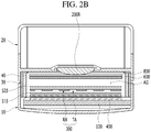
- FIG. 2B is a view taken along II-II' of FIG. 1 .
- FIG. 3 is an enlarged view of P region in FIG. 2A .
- FIG. 4 is a view showing a barrier of the display device according to the embodiment of the present invention.
- FIG. 5 is a view showing the relative location of pixel regions of a display panel and transmitting regions of a barrier in the display device according to the embodiment of the present invention.
- the display device may include an image member 10.
- the image member 10 may realize an image which is provided to a user.
- the image member 10 may realize an image for a virtual reality (VR) or an augmented reality (AR).
- VR virtual reality
- AR augmented reality
- the image member 10 may be fixed to the front of the user's eye by a mounting member 20.
- the display device may be a head mounted display apparatus (HMD) mounted on the user' head.
- the mounting member 20 may be a shape like a leg of an eyeglass frame.
- the mounting member 20 may be extended from the image member 10 in a direction.
- the mounting member 20 may be coupled to the image member 10 by a coupling member 30.
- the coupling member 30 may be a plate shape including a first end portion coupling to the image member 10, and a second end portion coupling to the mounting member 20.
- the coupling member 30 may be disposed at the inside of the image member 10 and the inside of the mounting member 20.
- the display device according to the embodiment of the present invention is described that the location of the image member 10 is fixed by using the user's ears, such as an eyeglass.
- the display device according to another embodiment of the present invention may include the image member 10 supported by other parts of the user.
- the display device according to another embodiment of the present invention may be a head gear shape which is worn on the user's head.
- a display panel 100 may be disposed in the image member 10.
- the display panel 100 may be disposed on an inner surface of the image member 10.
- the image member 10 may include a supporting part 11 supporting the display panel 100, and a coupling part 12 protruding from an edge of the supporting part 11.
- the coupling member 30 may be coupled to the coupling part 12 of the image member 10.
- the coupling part 12 may be surround side surfaces of the display panel 100.
- the display panel 100 may generate the image which is provided to the user.
- the display panel 100 may include pixel regions PX.
- Each of the pixel regions PX may include a light-emitting element 140 which emits light displaying a specific color.
- the light-emitting element 140 may include a lower electrode 141, a light-emitting layer 142 and an upper electrode 143, which are sequentially stacked.
- the light-emitting layer 142 may include an emission material layer (EML) formed of an organic material, an inorganic material or a hybrid material.
- EML emission material layer
- the display panel 100 of the display device according to the embodiment of the present invention may be an OLED panel.
- the light-emitting element 140 may be disposed between a lower substrate 110 and an upper substrate 180.
- a thin film transistor 120 may be disposed between the lower substrate 110 and the light-emitting element 140.
- the light-emitting element 140 may be controlled by the thin film transistor 120.
- the lower electrode 141 of the light-emitting element 140 may be in direct contact with a portion of the thin film transistor 120.
- An over-coat layer 130 may be disposed between the thin film transistor 120 and the light-emitting element 140.
- the over-coat layer 130 may remove a thickness difference due to the thin film transistor 120.
- the over-coat layer 130 may include an electrode contact hole exposing the portion of the thin film transistor 120.
- a bank insulating layer 150 may be disposed on the over-coat layer 130.
- the bank insulating layer 150 may cover an edge of the lower electrode 141.
- the light-emitting layer 142 and the upper electrode 143 may be stacked on a portion of the lower electrode 141 exposed by the bank insulating layer 150.
- the light-emitting layer 142 and/or the upper electrode 143 may be extended on the bank insulating layer 150.
- An upper passivation layer 160 may be disposed on the light-emitting element 140.
- the upper passivation layer 160 may prevent the damage of the light-emitting element 140 due to the external impact and moisture.
- a filling element 170 may be disposed between the upper passivation layer 160 and the upper substrate 180.
- the filling element 170 may include an adhesive material.
- the upper substrate 180 may be coupled to the lower substrate 110 in which the light-emitting element 140 is formed, by the filling element 170.
- the filling element 170 may have a multi-layer structure.
- the filling element 170 may include a lower filling layer 171 and an upper filling layer 172, which are sequentially stacked.
- the upper filling layer 172 may include a moisture-absorbing material 170p. The stress applied to the light-emitting element 140 due to the expansion of the moisture-absorbing material 170p may be relieved by the lower filling layer 171.
- An eyepiece 200 may be disposed on the display panel 100.
- the light emitted from the display panel 100 may be provided to the user passing through the eyepiece 200.
- the image realized by the display panel 100 may be recognized to the user through the eyepiece 200.
- the eyepiece 200 may be aligned with the user's eye by the mounting member 20.
- the eyepiece 200 may include a left lens 200L aligned with the left eye of the user, and a right lens 200R aligned with the right eye of the user.
- the position of the eyepiece 200 may be fixed by the image member 10.
- the eyepiece 200 may be coupled to a region of the image member 10.
- Optical elements may be disposed between the display panel 100 and the eyepiece 200 to increase a path of light travelling toward the eyepiece 200 from the display panel 100.
- a barrier 300, a front linear polarizer 400, a front quarter-wave plate 510, a rear quarter-wave plate 520, a reflective polarizing plate 600 and a rear linear polarizer 700 may be disposed between the display panel 100 and the eyepiece 200.
- the barrier 300 may be disposed between the display panel 100 and the eyepiece 200.
- the barrier 300 may reflect or transmit the light emitted from the display panel 100 on a region-by-region (in other words, on a region-by-region basis; in still other words, in a region-by-region manner).
- the barrier 300 may include reflecting regions RA and transmitting regions TA. Each of the transmitting regions TA may be disposed between the reflecting regions RA.
- the reflecting regions RA may reflect the light incident on the barrier 300.
- the light incident on the transmitting regions TA of the barrier 300 may transmit the barrier 300.
- the barrier 300 may include a supporting substrate 310 and reflective patterns 320 disposed on the supporting substrate 310.
- the supporting substrate 310 may include a transparent material.
- the supporting substrate 310 may include glass or plastic.
- the reflective patterns 320 may include a material having high reflectance.
- the reflective patterns 320 may include a metal, such as aluminum (Al) and silver (Ag).
- the reflective patterns 320 may overlap the reflecting regions RA.
- the light incident on the reflecting regions RA of the barrier 300 may be reflected by the reflective patterns 320.
- the transmitting regions TA may include a portion of the supporting substrate 310 exposed by the reflective patterns 320.
- the transmitting regions TA of the barrier 300 may overlap the pixel regions PX of the display panel 100.
- the width w1 and the length d1 of each pixel region PX may be smaller than the width w2 and the length d2 of the corresponding transmitting region TA.
- the pixel regions PX may be disposed inside the transmitting regions TA.
- the relative location of the transmitting regions TA with respect to the pixel regions PX may be constant on the entire surface of the display panel 100.
- the center of each pixel region PX may be the same as the center of the corresponding transmitting region TA.
- the front linear polarizer 400 may be disposed between the display panel 100 and the barrier 300.
- the front linear polarizer 400 may include a transmission axis in a first direction.
- the light passing through the front linear polarizer 400 may be linearly polarized in the first direction.
- the front quarter-wave plate 510 may be disposed between the front linear polarizer 400 and the barrier 300.
- the front linear polarizer 400 may be disposed between the display panel 100 and the front quarter-wave plate 510.
- the front quarter-wave plate 510 may delay the phase of incident light by ⁇ /4.
- the light passing through the front quarter-wave plate 510 may be circularly polarized.
- the rear quarter-wave plate 520 may be disposed between the barrier 300 and the eyepiece 200.
- the barrier 300 may be disposed between the front quarter-wave plate 510 and the rear quarter-wave plate 520.
- the rear quarter-wave plate 520 may delay the phase of incident light.
- the phase of the light passing through the rear quarter-wave plate 520 may be delayed in a direction opposite to the phase of the light passing through the front quarter-wave plate 510.
- the rear quarter-wave plate 520 may delay the phase of incident light by - ⁇ /4.
- the light circularly polarized by the front quarter-wave plate 510 may be linearly polarized in a direction same as the light incident on the front quarter-wave plate 510 by the rear quarter-wave plate 520.
- the reflective polarizing plate 600 may be disposed between the rear quarter-wave plate 520 and the eyepiece 200.
- the rear quarter-wave plate 520 may be disposed between the barrier 300 and the reflective polarizing plate 600.
- the reflective polarizing plate 600 may reflect the light linearly polarized in a specific direction.
- the reflective polarizing plate 600 may reflect the light linearly polarized in the first direction.
- the light linearly polarized in a second direction perpendicular to the first direction may transmit the reflective polarizing plate 600.
- the reflective polarizing plate 600 may include an advanced polarizing film (APF) or a dual brightness enhanced film (DBEF).
- APF advanced polarizing film
- DBEF dual brightness enhanced film
- the reflective polarizing plate 600 may be disposed close to the eyepiece 200.
- an air-gap AG may be disposed between the rear quarter-wave plate 520 and the reflective polarizing plate 600.
- the rear linear polarizer 700 may be disposed between the reflective polarizing plate 600 and the eyepiece 200.
- the transmission axis of the rear linear polarizer 700 may be parallel with the transmission axis of the reflective polarizing plate 600.
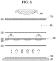
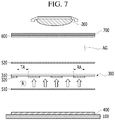
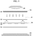
- FIGS. 6 to 13 are views sequentially showing the moving direction and the polarized state of light travelling toward an eyepiece from a display panel in the display device according to the embodiment of the present invention.
- the light emitted from the display panel 100 of the display device according to the embodiment of the present invention may pass through the front linear polarizer 400, as shown in FIG. 6 .
- the light passing through the front linear polarizer 400 may move toward the front quarter-wave plate 510.
- the light passing through the front linear polarizer 400 may be linearly polarized in the first direction.
- the light incident on the front quarter-wave plate 510 may be the light linearly polarized in the first direction.
- the light passing through the front quarter-wave plate 510 may move toward the reflecting regions RA and the transmitting regions TA of the barrier 300, as shown in FIG. 7 .
- the light passing through the front quarter-wave plate 510 may be circularly polarized.
- the light linearly polarized in the first direction by the front linear polarizer 400 may be right-circularly polarized by the front quarter-wave plate 510.
- the light incident on the barrier 300 may be the light right-circularly polarized.
- the light incident on the barrier 300 may be reflected or transmitted on a region-by-region (in other words, on a region-by-region basis; in still other words, in a region-by-region manner), as shown in FIG. 8 .
- the light incident on the reflecting regions RA of the barrier 300 may be reflected toward the display panel 100 by the reflective patterns 320. Since the light incident on the barrier 300 is the light which is right-circularly polarized, the light reflected by the reflective patterns 320 may be the light which is left-circularly polarized.
- the light incident on the transmitting regions TA of the barrier 300 may transmit the barrier 300.
- the light passing through the barrier 300 may move toward the rear quarter-wave plate 520.
- the light incident on the rear quarter-wave plate 520 passing through the transmitting regions TA of the barrier 300 may be the light which is right-circularly polarized.
- the light passing through the rear quarter-wave plate 520 may move toward the reflective polarizing plate 600, as shown in FIG. 9 .
- the rear quarter-wave plate 520 may delay the phase of the light in a direction opposite to the front quarter-wave plate 510.
- the light which is right-circularly polarized may become the light linearly polarized in the first direction by the rear quarter-wave plate 520.
- the light incident on the reflective polarizing plate 600 may be the light linearly polarized in the first direction.
- the light which is linearly polarized in the first direction may be reflected toward the barrier 300 by the reflective polarizing plate 600, as shown in FIG. 10 .
- the transmission axis of the reflective polarizing plate 600 may be perpendicular to the transmission axis of the front linear polarizer 400.
- the light reflected by the reflective polarizing plate 600 may transmit the rear quarter-wave plate 520, as shown in FIG. 11 .
- the light passing through the rear quarter-wave plate 520 may move toward the barrier 300. Since the rear quarter-wave plate 520 delays the phase of the light in a direction opposite to the front quarter-wave plate 510, the light incident on the barrier 300 after passing through the rear quarter-wave plate 520 may be the light which is right-circularly polarized. The rotation direction of the polarized light incident on the barrier 300 after passing through the rear quarter-wave plate 520 may be opposite to the rotation direction of the polarized light incident on the rear quarter-wave plate 520 after passing through the transmitting regions TA of the barrier 300.
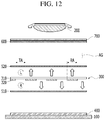
- the light moving toward the barrier 300 from the rear quarter-wave plate 520 may be reflected or transmitted on a region-by-region (in other words, on a region-by-region basis; in still other words, in a region-by-region manner) by the reflecting regions RA and the transmitting regions TA of the barrier 300, as shown in FIG. 12 .
- the light incident on the transmitting regions TA of the barrier 300 may transmit the barrier 300 and move toward the front quarter-wave plate 510.
- the light incident on the reflecting regions RA of the barrier 300 may be reflected again toward the rear quarter-wave plate 520 by the reflective patterns 320. Since the light travelling toward the barrier 300 from the rear quarter-wave plate 520 is the light which is right-circularly polarized, the light reflected again toward the rear quarter-wave plate 520 by the reflective patterns 320 of the barrier 300 may be the light which is left-circularly polarized.
- the light reflected again by the reflective patterns 320 may transmit the rear quarter-wave plate 520, as shown in FIG. 13 .
- the light passing through the rear quarter-wave plate 520 may move toward the reflective polarizing plate 600. Since the light reflected again by the reflective patterns 320 is the light which is left-circularly polarized, the light incident again on the reflective polarizing plate 600 after passing through the rear quarter-wave plate 520 may be the light which is linearly polarized in the second direction perpendicular to the first direction. Since the transmission axis of the reflective polarizing plate 600 is perpendicular to the transmission axis of the front linear polarizer 400, the light which is linearly polarized by the rear quarter-wave plate 520 may transmit the reflective polarizing plate 600. Thus, in the display device according to the embodiment of the present invention, the path of the light travelling toward the eyepiece 200 from the display panel 100 may be increased by twice of a distance between the barrier 300 and the reflective polarizing plate 600.
- the display device may increase the path of the light travelling toward the eyepiece 200 from the display panel 100 by the barrier 300 including the reflecting regions RA and the transmitting regions TA. That is, in the display device according to the embodiment of the present invention, the light moving toward the eyepiece 200 from the display panel 100 may not pass through an element that reduces the amount of the light passing through, such as a half-mirror. Thus, in the display device according to the embodiment of the present invention, the characteristic of the light provided to the user through the eyepiece 200 may be maintained, constantly. Therefore, in the display device according to the embodiment of the present invention, the light extraction efficiency may be increased without the change of the resolution.
- each of the pixel regions PX may be disposed inside the corresponding transmitting region TA, so that the light travelling toward the rear quarter-wave plate 520 from the display panel 100 through the transmitting regions TA of the barrier 300 may be maximized.
- the quality and the color reproduction rate of the image provided to the user may be improved, efficiently.
- each transmitting region TA is constant on the entire surface of the display panel 100.
- the relative location of each transmitting region TA may be changed according to the position of the corresponding transmitting region TA in the display panel 100.
- the center of each transmitting region TA may be disposed closer to the center of the display panel 100 than the center of the corresponding pixel region PX, as shown in FIG. 14 . That is, in the display device according to another embodiment of the present invention, each of transmitting regions TA may be disposed closer to the central portion of the display panel 100 than the corresponding pixel region PX.
- the amount of the light provided to the user may be increased. Therefore, in the display device according to another embodiment of the present invention, the light extraction efficiency may be increased, efficiently.
- each of the transmitting regions TA of the barrier 300 may be a bar shape extending in a direction, as shown in FIG. 15 .
- the process of forming the barrier 300 may be simplified. Therefore, in the display device according to another embodiment of the present invention, the light extraction efficiency and the productivity may be increased without the deterioration of the resolution.
- the reflective patterns 320 are disposed between the front quarter-wave plate 510 and the supporting substrate 310.
- the reflective patterns 320 may be disposed on a surface of the supporting substrate 310 facing the eyepiece 200, as shown in FIG. 16 .
- the degree of freedom for the location and the forming process of the barrier 300 may be increased. Therefore, in the display device according to another embodiment of the present invention, the light extraction efficiency and the productivity may be efficiently increased without the deterioration of the resolution.
- the display device is described that the barrier 300 including the supporting substrate 310 and the reflective patterns 320 is disposed between the front quarter-wave plate 510 and the rear quarter-wave plate 520.
- the display device may include the reflective patterns 320 disposed on a surface of the front quarter-wave plate 510 facing the eyepiece 200, as shown in FIG. 17 . That is, in the display device according to another embodiment of the present invention, a portion of the front quarter-wave plate 510 exposed by the reflective patterns 320 may overlap the pixel regions of the display panel 100. Thus, in the display device according to another embodiment of the present invention, the light reflected toward the display panel 100 by the reflective patterns 320 may be minimized.
- the path of the light increased by the reflective patterns 320 may be adjusted, efficiently.
- the front linear polarizer 400 may be in direct contact with the display panel 100 and the front quarter-wave plate 510. Therefore, in the display device according to another embodiment of the present invention, the overall thickness may be reduced, and the light extraction efficiency may be increased without the deterioration of the resolution.
- the display device may include the front linear polarizer, a front quarter-wave plate, a barrier, a rear quarter-wave plate and a reflective polarizing plate between a display panel and an eyepiece, the barrier exposing a portion of the front quarter-wave plate.
- the loss of the light between the eyepiece and the display panel may be minimized, and the path of the light travelling toward the eyepiece from the display panel may be increased. That is, in the display device according to the embodiments of the present invention, the light extraction efficiency may be increased without the deterioration of the resolution. Thereby, in the display device according to the embodiments of the present invention, the quality and the color reproduction rate of the image recognized to the user may be improved.
Landscapes
- Physics & Mathematics (AREA)
- Optics & Photonics (AREA)
- General Physics & Mathematics (AREA)
- Polarising Elements (AREA)
- Electroluminescent Light Sources (AREA)
Abstract
Description
- This application claims the priority benefit of Korean Patent Application No.
10-2017-0179352, filed on December 26, 2017 - The present invention relates to a display device in which an image realized by a display panel is provided through an eyepiece.
- Generally, a display device includes a display panel which realizes an image. For example, the display device may include a liquid crystal panel having a liquid crystal, and/or an Organic Light-Emitting Diode (OLED) panel having an organic light-emitting element.
- The display device may provide an image realized by the display panel to a user through an eyepiece. For example, the display device may be a head mounted display apparatus (HMD) including an image member accommodating the display panel, an eyepiece coupled to the image member and a mounting member for aligning the eyepiece with the user's eye.
- In the display device, the resolution of the image provided to the user may be determined according to a length of a path of light travelling toward the eyepiece from the display panel. For example, the resolution of the display device may be proportional with the length of the path of light travelling toward the eyepiece from the display panel. Thus, the display device may increase the path of light travelling toward the eyepiece from the display panel by using a half-mirror, in order to improve the resolution without the change of the overall thickness. However, in the display device, the amount of the light emitted to the outside may be reduced by the half-mirror.
- Accordingly, the present invention is directed to a display device that substantially obviates one or more problems due to limitations and disadvantages of the related art.
- An object of the present invention is to provide a display device capable of increasing the light extraction efficiency without the deterioration of the resolution.
- Another object of the present invention is to provide a display device in which a path of light travelling toward an eyepiece from a display panel may be increased, and the loss of the light between the display panel and the eyepiece may be minimized.
- Additional advantages, objects, and features of the invention will be set forth in part in the description which follows and in part will become apparent to those having ordinary skill in the art upon examination of the following or may be learned from practice of the invention. The objectives and other advantages of the invention may be realized and attained by the structure particularly pointed out in the written description and claims hereof as well as the appended drawings.
- To achieve these objects and other advantages and in accordance with the purpose of the invention, as embodied and broadly described herein, there is provided a display device according to claim 1. Further embodiments are described in the dependent claims. According to an aspect of the present invention, there is provided a display device including a front quarter-wave plate between a display panel and an eyepiece. A rear quarter-wave plate is disposed between the front quarter-wave plate and the eyepiece. A front linear polarizer is disposed between the display panel and the front quarter-wave plate. A reflective polarizing plate is disposed between the rear quarter-wave plate and the eyepiece. A barrier is disposed between the front quarter-wave plate and the rear quarter-wave plate. The barrier includes reflecting regions and transmitting regions between the reflecting regions. Each of the transmitting regions may be disposed between the reflecting regions.
- The barrier may include a supporting substrate and reflective patterns. The reflective patterns may be disposed on the supporting substrate. The reflective patterns may overlap the reflecting regions.
- The reflective patterns may include a metal.
- The reflective patterns may be disposed on a surface of the supporting substrate facing the display panel.
- The display panel may include pixel regions. The pixel regions of the display panel may overlap the transmitting regions of the barrier.
- Each of the transmitting regions may have a size larger than the corresponding pixel region.
- Each of the transmitting regions may be disposed closer to the center of the display panel than the corresponding pixel region.
- The display panel may include a lower substrate, an upper substrate, and a light-emitting element between the lower substrate and the upper substrate.
- The display panel may include pixel regions. The barrier may include reflective patterns, the reflective patterns exposing a portion of the front quarter-wave plate. The pixel regions of the display panel may overlap the portion of the front quarter-wave plate exposed by the reflective patterns.
- The portion of the front quarter-wave plate exposed by the reflective patterns may be a bar-shape extending in a direction.
- The reflective patterns may be in direct contact with the front quarter-wave plate.
- The front linear polarizer may be in direct contact with the display panel and the front quarter-wave plate.
- A phase of light passing through the rear quarter-wave plate may be delayed in a direction opposite to a phase of light passing through the front quarter-wave plate.
- A polarized state of light passing through the reflective polarizing plate may be perpendicular to a polarized state of the light passing through the front linear polarizer.
- The display device may further include a rear linear polarizer between the reflective polarizing plate and the eyepiece, wherein the transmission axis of the rear linear polarizer is parallel with the transmission axis of the reflective polarizing plate.
- In another aspect of the present invention, there is provided a display device including a display panel. The display panel includes pixel regions. A front linear polarizer is disposed on the display panel. A front quarter-wave plate is disposed on the front linear polarizer. A rear quarter-wave plate is disposed on the front quarter-wave plate. A reflective polarizing plate is disposed on the rear quarter-wave plate. An eyepiece is disposed on the reflective polarizing plate. Reflective patterns are disposed between the front quarter-wave plate and the rear quarter-wave plate. The reflective patterns expose a portion of the front quarter-wave plate. The pixel regions of the display panel overlap the portion of the front quarter-wave plate exposed by the reflective patterns.
- The portion of the front quarter-wave plate exposed by the reflective patterns may be a bar shape extending in a direction.
- The reflective patterns may be in direct contact with the front quarter-wave plate.
- The front linear polarizer may be in direct contact with the display panel and the front quarter-wave plate.
- A phase of light passing through the rear quarter-wave plate may be delayed in a direction opposite to a phase of light passing through the front quarter-wave plate.
- The polarized state of light passing through the reflective polarizing plate may be perpendicular to the polarized state of light passing through the front linear polarizer.
- A rear linear polarizer may be disposed between the reflective polarizing plate and the eyepiece. The transmission axis of the rear linear polarizer may be parallel with the transmission axis of the reflective polarizing plate.
- The accompanying drawings, which are included to provide a further understanding of the invention and are incorporated in and constitute a part of this application, illustrate embodiment(s) of the invention and together with the description serve to explain the principle of the invention. In the drawings:
-
FIG. 1 is a view schematically showing a display device according to an embodiment of the present invention; -
FIG. 2A is a view taken along I-I' ofFIG. 1 ; -
FIG. 2B is a view taken along II-II' ofFIG. 1 ; -
FIG. 3 is an enlarged view of P region inFIG. 2A ; -
FIG. 4 is a view showing a barrier of the display device according to the embodiment of the present invention; -
FIG. 5 is a view showing the relative location of pixel regions of a display panel and transmitting regions of a barrier in the display device according to the embodiment of the present invention; -
FIGS. 6 to 13 are views sequentially showing the moving direction and the polarized state of light travelling toward an eyepiece from a display panel in the display device according to the embodiment of the present invention; -
FIGS. 14 to 17 are views respectively showing the display device according to another embodiment of the present invention. - Hereinafter, details related to the above objects, technical configurations, and operational effects of the embodiments of the present invention will be clearly understood by the following detailed description with reference to the drawings, which illustrate some embodiments of the present invention. Here, the embodiments of the present invention are provided in order to allow the technical sprit of the present invention to be satisfactorily transferred to those skilled in the art, and thus the present invention may be embodied in other forms and is not limited to the embodiments described below.
- In addition, the same or extremely similar elements may be designated by the same reference numerals throughout the specification, and in the drawings, the lengths and thickness of layers and regions may be exaggerated for convenience. It will be understood that, when a first element is referred to as being "on" a second element, although the first element may be disposed on the second element so as to come into contact with the second element, a third element may be interposed between the first element and the second element.
- Here, terms such as, for example, "first" and "second" may be used to distinguish any one element with another element. However, the first element and the second element may be arbitrary named according to the convenience of those skilled in the art without departing the technical sprit of the present invention.
- The terms used in the specification of the present invention are merely used in order to describe particular embodiments, and are not intended to limit the scope of the present invention. For example, an element described in the singular form is intended to include a plurality of elements unless the context clearly indicates otherwise. In addition, in the specification of the present invention, it will be further understood that the terms "comprises" and "includes" specify the presence of stated features, integers, steps, operations, elements, components, and/or combinations thereof, but do not preclude the presence or addition of one or more other features, integers, steps, operations, elements, components, and/or combinations.
- Unless otherwise defined, all terms (including technical and scientific terms) used herein have the same meaning as commonly understood by one of ordinary skill in the art to which example embodiments belong. It will be further understood that terms, such as those defined in commonly used dictionaries, should be interpreted as having a meaning that is consistent with their meaning in the context of the relevant art and should not be interpreted in an idealized or overly formal sense unless expressly so defined herein.
-
FIG. 1 is a view schematically showing a display device according to an embodiment of the present invention.FIG. 2A is a view taken along I-I' ofFIG. 1 .FIG. 2B is a view taken along II-II' ofFIG. 1 .FIG. 3 is an enlarged view of P region inFIG. 2A .FIG. 4 is a view showing a barrier of the display device according to the embodiment of the present invention.FIG. 5 is a view showing the relative location of pixel regions of a display panel and transmitting regions of a barrier in the display device according to the embodiment of the present invention. - Referring
FIGS. 1, 2A ,2B and3 to 5 , the display device according to the embodiment of the present invention may include animage member 10. Theimage member 10 may realize an image which is provided to a user. For example, theimage member 10 may realize an image for a virtual reality (VR) or an augmented reality (AR). - The
image member 10 may be fixed to the front of the user's eye by a mountingmember 20. For example, the display device according to the embodiment of the present invention may be a head mounted display apparatus (HMD) mounted on the user' head. The mountingmember 20 may be a shape like a leg of an eyeglass frame. For example, the mountingmember 20 may be extended from theimage member 10 in a direction. The mountingmember 20 may be coupled to theimage member 10 by acoupling member 30. For example, thecoupling member 30 may be a plate shape including a first end portion coupling to theimage member 10, and a second end portion coupling to the mountingmember 20. Thecoupling member 30 may be disposed at the inside of theimage member 10 and the inside of the mountingmember 20. - The display device according to the embodiment of the present invention is described that the location of the
image member 10 is fixed by using the user's ears, such as an eyeglass. However, the display device according to another embodiment of the present invention may include theimage member 10 supported by other parts of the user. For example, the display device according to another embodiment of the present invention may be a head gear shape which is worn on the user's head. - A
display panel 100 may be disposed in theimage member 10. Thedisplay panel 100 may be disposed on an inner surface of theimage member 10. For example, theimage member 10 may include a supportingpart 11 supporting thedisplay panel 100, and acoupling part 12 protruding from an edge of the supportingpart 11. Thecoupling member 30 may be coupled to thecoupling part 12 of theimage member 10. Thecoupling part 12 may be surround side surfaces of thedisplay panel 100. - The
display panel 100 may generate the image which is provided to the user. For example, thedisplay panel 100 may include pixel regions PX. Each of the pixel regions PX may include a light-emittingelement 140 which emits light displaying a specific color. For example, the light-emittingelement 140 may include alower electrode 141, a light-emittinglayer 142 and anupper electrode 143, which are sequentially stacked. The light-emittinglayer 142 may include an emission material layer (EML) formed of an organic material, an inorganic material or a hybrid material. For example, thedisplay panel 100 of the display device according to the embodiment of the present invention may be an OLED panel. - The light-emitting
element 140 may be disposed between alower substrate 110 and anupper substrate 180. Athin film transistor 120 may be disposed between thelower substrate 110 and the light-emittingelement 140. The light-emittingelement 140 may be controlled by thethin film transistor 120. For example, thelower electrode 141 of the light-emittingelement 140 may be in direct contact with a portion of thethin film transistor 120. Anover-coat layer 130 may be disposed between thethin film transistor 120 and the light-emittingelement 140. Theover-coat layer 130 may remove a thickness difference due to thethin film transistor 120. Theover-coat layer 130 may include an electrode contact hole exposing the portion of thethin film transistor 120. - A
bank insulating layer 150 may be disposed on theover-coat layer 130. Thebank insulating layer 150 may cover an edge of thelower electrode 141. The light-emittinglayer 142 and theupper electrode 143 may be stacked on a portion of thelower electrode 141 exposed by thebank insulating layer 150. The light-emittinglayer 142 and/or theupper electrode 143 may be extended on thebank insulating layer 150. - An
upper passivation layer 160 may be disposed on the light-emittingelement 140. Theupper passivation layer 160 may prevent the damage of the light-emittingelement 140 due to the external impact and moisture. A fillingelement 170 may be disposed between theupper passivation layer 160 and theupper substrate 180. The fillingelement 170 may include an adhesive material. For example, theupper substrate 180 may be coupled to thelower substrate 110 in which the light-emittingelement 140 is formed, by the fillingelement 170. The fillingelement 170 may have a multi-layer structure. For example, the fillingelement 170 may include alower filling layer 171 and anupper filling layer 172, which are sequentially stacked. Theupper filling layer 172 may include a moisture-absorbingmaterial 170p. The stress applied to the light-emittingelement 140 due to the expansion of the moisture-absorbingmaterial 170p may be relieved by thelower filling layer 171. - An
eyepiece 200 may be disposed on thedisplay panel 100. The light emitted from thedisplay panel 100 may be provided to the user passing through theeyepiece 200. The image realized by thedisplay panel 100 may be recognized to the user through theeyepiece 200. Theeyepiece 200 may be aligned with the user's eye by the mountingmember 20. For example, theeyepiece 200 may include aleft lens 200L aligned with the left eye of the user, and aright lens 200R aligned with the right eye of the user. The position of theeyepiece 200 may be fixed by theimage member 10. For example, theeyepiece 200 may be coupled to a region of theimage member 10. - Optical elements may be disposed between the
display panel 100 and theeyepiece 200 to increase a path of light travelling toward theeyepiece 200 from thedisplay panel 100. For example, abarrier 300, a frontlinear polarizer 400, a front quarter-wave plate 510, a rear quarter-wave plate 520, a reflectivepolarizing plate 600 and a rearlinear polarizer 700 may be disposed between thedisplay panel 100 and theeyepiece 200. - The
barrier 300 may be disposed between thedisplay panel 100 and theeyepiece 200. Thebarrier 300 may reflect or transmit the light emitted from thedisplay panel 100 on a region-by-region (in other words, on a region-by-region basis; in still other words, in a region-by-region manner). For example, thebarrier 300 may include reflecting regions RA and transmitting regions TA. Each of the transmitting regions TA may be disposed between the reflecting regions RA. - The reflecting regions RA may reflect the light incident on the
barrier 300. The light incident on the transmitting regions TA of thebarrier 300 may transmit thebarrier 300. For example, thebarrier 300 may include a supportingsubstrate 310 andreflective patterns 320 disposed on the supportingsubstrate 310. The supportingsubstrate 310 may include a transparent material. For example, the supportingsubstrate 310 may include glass or plastic. Thereflective patterns 320 may include a material having high reflectance. For example, thereflective patterns 320 may include a metal, such as aluminum (Al) and silver (Ag). Thereflective patterns 320 may overlap the reflecting regions RA. The light incident on the reflecting regions RA of thebarrier 300 may be reflected by thereflective patterns 320. The transmitting regions TA may include a portion of the supportingsubstrate 310 exposed by thereflective patterns 320. - The transmitting regions TA of the
barrier 300 may overlap the pixel regions PX of thedisplay panel 100. The width w1 and the length d1 of each pixel region PX may be smaller than the width w2 and the length d2 of the corresponding transmitting region TA. For example, the pixel regions PX may be disposed inside the transmitting regions TA. The relative location of the transmitting regions TA with respect to the pixel regions PX may be constant on the entire surface of thedisplay panel 100. For example, the center of each pixel region PX may be the same as the center of the corresponding transmitting region TA. - The front
linear polarizer 400 may be disposed between thedisplay panel 100 and thebarrier 300. The frontlinear polarizer 400 may include a transmission axis in a first direction. For example, the light passing through the frontlinear polarizer 400 may be linearly polarized in the first direction. - The front quarter-
wave plate 510 may be disposed between the frontlinear polarizer 400 and thebarrier 300. The frontlinear polarizer 400 may be disposed between thedisplay panel 100 and the front quarter-wave plate 510. The front quarter-wave plate 510 may delay the phase of incident light by λ/4. For example, the light passing through the front quarter-wave plate 510 may be circularly polarized. - The rear quarter-
wave plate 520 may be disposed between thebarrier 300 and theeyepiece 200. Thebarrier 300 may be disposed between the front quarter-wave plate 510 and the rear quarter-wave plate 520. The rear quarter-wave plate 520 may delay the phase of incident light. The phase of the light passing through the rear quarter-wave plate 520 may be delayed in a direction opposite to the phase of the light passing through the front quarter-wave plate 510. For example, the rear quarter-wave plate 520 may delay the phase of incident light by -λ/4. The light circularly polarized by the front quarter-wave plate 510 may be linearly polarized in a direction same as the light incident on the front quarter-wave plate 510 by the rear quarter-wave plate 520. - The reflective
polarizing plate 600 may be disposed between the rear quarter-wave plate 520 and theeyepiece 200. The rear quarter-wave plate 520 may be disposed between thebarrier 300 and the reflectivepolarizing plate 600. The reflectivepolarizing plate 600 may reflect the light linearly polarized in a specific direction. For example, the reflectivepolarizing plate 600 may reflect the light linearly polarized in the first direction. The light linearly polarized in a second direction perpendicular to the first direction may transmit the reflectivepolarizing plate 600. The reflectivepolarizing plate 600 may include an advanced polarizing film (APF) or a dual brightness enhanced film (DBEF). - The reflective
polarizing plate 600 may be disposed close to theeyepiece 200. For example, an air-gap (AG) may be disposed between the rear quarter-wave plate 520 and the reflectivepolarizing plate 600. - The rear
linear polarizer 700 may be disposed between the reflectivepolarizing plate 600 and theeyepiece 200. The transmission axis of the rearlinear polarizer 700 may be parallel with the transmission axis of the reflectivepolarizing plate 600. -
FIGS. 6 to 13 are views sequentially showing the moving direction and the polarized state of light travelling toward an eyepiece from a display panel in the display device according to the embodiment of the present invention. - The movement path and the polarized state of the light emitted from the
display panel 100 of the display device according to the embodiment of the present invention will be described with reference toFIGS. 6 to 13 . First, the light emitted from thedisplay panel 100 of the display device according to the embodiment of the present invention may pass through the frontlinear polarizer 400, as shown inFIG. 6 . - The light passing through the front
linear polarizer 400 may move toward the front quarter-wave plate 510. The light passing through the frontlinear polarizer 400 may be linearly polarized in the first direction. For example, the light incident on the front quarter-wave plate 510 may be the light linearly polarized in the first direction. - In the display device according to the embodiment of the present invention, the light passing through the front quarter-
wave plate 510 may move toward the reflecting regions RA and the transmitting regions TA of thebarrier 300, as shown inFIG. 7 . - The light passing through the front quarter-
wave plate 510 may be circularly polarized. For example, the light linearly polarized in the first direction by the frontlinear polarizer 400 may be right-circularly polarized by the front quarter-wave plate 510. The light incident on thebarrier 300 may be the light right-circularly polarized. - In the display device according to the embodiment of the present invention, the light incident on the
barrier 300 may be reflected or transmitted on a region-by-region (in other words, on a region-by-region basis; in still other words, in a region-by-region manner), as shown inFIG. 8 . - The light incident on the reflecting regions RA of the
barrier 300 may be reflected toward thedisplay panel 100 by thereflective patterns 320. Since the light incident on thebarrier 300 is the light which is right-circularly polarized, the light reflected by thereflective patterns 320 may be the light which is left-circularly polarized. - The light incident on the transmitting regions TA of the
barrier 300 may transmit thebarrier 300. The light passing through thebarrier 300 may move toward the rear quarter-wave plate 520. For example, the light incident on the rear quarter-wave plate 520 passing through the transmitting regions TA of thebarrier 300 may be the light which is right-circularly polarized. - In the display device according to the embodiment of the present invention, the light passing through the rear quarter-
wave plate 520 may move toward the reflectivepolarizing plate 600, as shown inFIG. 9 . - The rear quarter-
wave plate 520 may delay the phase of the light in a direction opposite to the front quarter-wave plate 510. For example, the light which is right-circularly polarized may become the light linearly polarized in the first direction by the rear quarter-wave plate 520. The light incident on the reflectivepolarizing plate 600 may be the light linearly polarized in the first direction. - In the display device according to the embodiment of the present invention, the light which is linearly polarized in the first direction may be reflected toward the
barrier 300 by the reflectivepolarizing plate 600, as shown inFIG. 10 . For example, the transmission axis of the reflectivepolarizing plate 600 may be perpendicular to the transmission axis of the frontlinear polarizer 400. - In the display device according to the embodiment of the present invention, the light reflected by the reflective
polarizing plate 600 may transmit the rear quarter-wave plate 520, as shown inFIG. 11 . - The light passing through the rear quarter-
wave plate 520 may move toward thebarrier 300. Since the rear quarter-wave plate 520 delays the phase of the light in a direction opposite to the front quarter-wave plate 510, the light incident on thebarrier 300 after passing through the rear quarter-wave plate 520 may be the light which is right-circularly polarized. The rotation direction of the polarized light incident on thebarrier 300 after passing through the rear quarter-wave plate 520 may be opposite to the rotation direction of the polarized light incident on the rear quarter-wave plate 520 after passing through the transmitting regions TA of thebarrier 300. - In the display device according to the embodiment of the present invention, the light moving toward the
barrier 300 from the rear quarter-wave plate 520 may be reflected or transmitted on a region-by-region (in other words, on a region-by-region basis; in still other words, in a region-by-region manner) by the reflecting regions RA and the transmitting regions TA of thebarrier 300, as shown inFIG. 12 . - The light incident on the transmitting regions TA of the
barrier 300 may transmit thebarrier 300 and move toward the front quarter-wave plate 510. The light incident on the reflecting regions RA of thebarrier 300 may be reflected again toward the rear quarter-wave plate 520 by thereflective patterns 320. Since the light travelling toward thebarrier 300 from the rear quarter-wave plate 520 is the light which is right-circularly polarized, the light reflected again toward the rear quarter-wave plate 520 by thereflective patterns 320 of thebarrier 300 may be the light which is left-circularly polarized. - In the display device according to the embodiment of the present invention, the light reflected again by the
reflective patterns 320 may transmit the rear quarter-wave plate 520, as shown inFIG. 13 . - The light passing through the rear quarter-
wave plate 520 may move toward the reflectivepolarizing plate 600. Since the light reflected again by thereflective patterns 320 is the light which is left-circularly polarized, the light incident again on the reflectivepolarizing plate 600 after passing through the rear quarter-wave plate 520 may be the light which is linearly polarized in the second direction perpendicular to the first direction. Since the transmission axis of the reflectivepolarizing plate 600 is perpendicular to the transmission axis of the frontlinear polarizer 400, the light which is linearly polarized by the rear quarter-wave plate 520 may transmit the reflectivepolarizing plate 600. Thus, in the display device according to the embodiment of the present invention, the path of the light travelling toward theeyepiece 200 from thedisplay panel 100 may be increased by twice of a distance between thebarrier 300 and the reflectivepolarizing plate 600. - Accordingly, the display device according to the embodiment of the present invention may increase the path of the light travelling toward the
eyepiece 200 from thedisplay panel 100 by thebarrier 300 including the reflecting regions RA and the transmitting regions TA. That is, in the display device according to the embodiment of the present invention, the light moving toward theeyepiece 200 from thedisplay panel 100 may not pass through an element that reduces the amount of the light passing through, such as a half-mirror. Thus, in the display device according to the embodiment of the present invention, the characteristic of the light provided to the user through theeyepiece 200 may be maintained, constantly. Therefore, in the display device according to the embodiment of the present invention, the light extraction efficiency may be increased without the change of the resolution. - Also, in the display device according to the embodiment of the present invention, each of the pixel regions PX may be disposed inside the corresponding transmitting region TA, so that the light travelling toward the rear quarter-
wave plate 520 from thedisplay panel 100 through the transmitting regions TA of thebarrier 300 may be maximized. Thus, in the display device according to the embodiment of the present invention, the quality and the color reproduction rate of the image provided to the user may be improved, efficiently. - The display device according to the embodiment of the present invention is described that the relative location of each transmitting region TA is constant on the entire surface of the
display panel 100. However, in the display device according to another embodiment of the present invention, the relative location of each transmitting region TA may be changed according to the position of the corresponding transmitting region TA in thedisplay panel 100. For example, in the display device according to another embodiment of the present invention, the center of each transmitting region TA may be disposed closer to the center of thedisplay panel 100 than the center of the corresponding pixel region PX, as shown inFIG. 14 . That is, in the display device according to another embodiment of the present invention, each of transmitting regions TA may be disposed closer to the central portion of thedisplay panel 100 than the corresponding pixel region PX. Thus, in the display device according to another embodiment of the present invention, the amount of the light provided to the user may be increased. Therefore, in the display device according to another embodiment of the present invention, the light extraction efficiency may be increased, efficiently. - The display device according to the embodiment of the present invention is described that the
reflective patterns 320 of thebarrier 300 overlap regions between the pixel regions PX of thedisplay panel 100. However, in the display device according to another embodiment of the present invention, each of the transmitting regions TA of thebarrier 300 may be a bar shape extending in a direction, as shown inFIG. 15 . Thus, in the display device according to another embodiment of the present invention, the process of forming thebarrier 300 may be simplified. Therefore, in the display device according to another embodiment of the present invention, the light extraction efficiency and the productivity may be increased without the deterioration of the resolution. - The display device according to the embodiment of the present invention is described that the
reflective patterns 320 are disposed between the front quarter-wave plate 510 and the supportingsubstrate 310. However, in the display device according to another embodiment of the present invention, thereflective patterns 320 may be disposed on a surface of the supportingsubstrate 310 facing theeyepiece 200, as shown inFIG. 16 . Thus, in the display device according to another embodiment of the present invention, the degree of freedom for the location and the forming process of thebarrier 300 may be increased. Therefore, in the display device according to another embodiment of the present invention, the light extraction efficiency and the productivity may be efficiently increased without the deterioration of the resolution. - The display device according to the embodiment of the present invention is described that the
barrier 300 including the supportingsubstrate 310 and thereflective patterns 320 is disposed between the front quarter-wave plate 510 and the rear quarter-wave plate 520. However, the display device according to another embodiment of the present invention may include thereflective patterns 320 disposed on a surface of the front quarter-wave plate 510 facing theeyepiece 200, as shown inFIG. 17 . That is, in the display device according to another embodiment of the present invention, a portion of the front quarter-wave plate 510 exposed by thereflective patterns 320 may overlap the pixel regions of thedisplay panel 100. Thus, in the display device according to another embodiment of the present invention, the light reflected toward thedisplay panel 100 by thereflective patterns 320 may be minimized. And, in the display device according to another embodiment of the present invention, the path of the light increased by thereflective patterns 320 may be adjusted, efficiently. For example, in the display device according to another embodiment of the present invention, the frontlinear polarizer 400 may be in direct contact with thedisplay panel 100 and the front quarter-wave plate 510. Therefore, in the display device according to another embodiment of the present invention, the overall thickness may be reduced, and the light extraction efficiency may be increased without the deterioration of the resolution. - In the result, the display device according to the embodiments of the present invention may include the front linear polarizer, a front quarter-wave plate, a barrier, a rear quarter-wave plate and a reflective polarizing plate between a display panel and an eyepiece, the barrier exposing a portion of the front quarter-wave plate. Thus, in the display device according to the embodiments of the present invention, the loss of the light between the eyepiece and the display panel may be minimized, and the path of the light travelling toward the eyepiece from the display panel may be increased. That is, in the display device according to the embodiments of the present invention, the light extraction efficiency may be increased without the deterioration of the resolution. Thereby, in the display device according to the embodiments of the present invention, the quality and the color reproduction rate of the image recognized to the user may be improved.
Claims (15)
- A display device comprising:a display panel (100) and an eyepiece (200);a front quarter-wave plate (510) between the display panel (100) and the eyepiece (200);a rear quarter-wave plate (520) between the front quarter-wave plate (510) and the eyepiece (200);a front linear polarizer (400) between the display panel (100) and the front quarter-wave plate (510);a reflective polarizing plate (600) between the rear quarter-wave plate (520) and the eyepiece (200); anda barrier (300) between the front quarter-wave plate (510) and the rear quarter-wave plate (520),wherein the barrier (300) includes reflecting regions (RA) and transmitting regions (TA) between the reflecting regions (RA).
- The display device according to claim 1, wherein the barrier (300) includes a supporting substrate (310) and reflective patterns (320) on the supporting substrate (310), and
wherein the reflective patterns (320) overlap the reflecting regions (RA). - The display device according to claim 2, wherein the reflective patterns (320) include a metal.
- The display device according to claim 2 or 3, wherein the reflective patterns (320) are disposed on a surface of the supporting substrate (310) facing the display panel (100).
- The display device according to any one of claims 1 to 4, wherein the display panel (100) includes pixel regions (PX), and
wherein the pixel regions (PX) overlap the transmitting regions (TA) of the barrier (300). - The display device according to claim 5, wherein each of the transmitting regions (TA) has a size larger than the corresponding pixel region (PX).
- The display device according to claim 6, wherein each of the transmitting regions (TA) is disposed closer to the center of the display panel (100) than the corresponding pixel region.
- The display device according to any one of claims 1 to 7, wherein the display panel (100) includes a lower substrate (110), an upper substrate (180), and a light-emitting element (140) between the lower substrate (110) and the upper substrate (180).
- The display device of claim 1, wherein:the display panel (100) includes pixel regions (PX); andthe barrier (300) includes reflective patterns (320), the reflective patterns (320) exposing a portion of the front quarter-wave plate (510),wherein the pixel regions (PX) of the display panel (100) overlap the portion of the front quarter-wave plate (510) exposed by the reflective patterns (320).
- The display device according to claim 9, wherein the portion of the front quarter-wave plate (510) exposed by the reflective patterns (320) is a bar-shape extending in a direction.
- The display device according to claim 9 or 10, wherein the reflective patterns (320) are in direct contact with the front quarter-wave plate (510).
- The display device according to claim 11, wherein the front linear polarizer (400) is in direct contact with the display panel (100) and the front quarter-wave plate (510) .
- The display device according to any one of claims 9 to 12, wherein a phase of light passing through the rear quarter-wave plate (520) is delayed in a direction opposite to a phase of light passing through the front quarter-wave plate (510).
- The display device according to claim 13, wherein a polarized state of light passing through the reflective polarizing plate (600) is perpendicular to a polarized state of the light passing through the front linear polarizer (400).
- The display device according to any one of claims 9 to 14, further comprising a rear linear polarizer (700) between the reflective polarizing plate (600) and the eyepiece (200),
wherein the transmission axis of the rear linear polarizer (700) is parallel with the transmission axis of the reflective polarizing plate (600).
Applications Claiming Priority (1)
| Application Number | Priority Date | Filing Date | Title |
|---|---|---|---|
| KR1020170179352A KR102490630B1 (en) | 2017-12-26 | 2017-12-26 | Display apparatus having an eyepiece |
Publications (2)
| Publication Number | Publication Date |
|---|---|
| EP3505992A1 true EP3505992A1 (en) | 2019-07-03 |
| EP3505992B1 EP3505992B1 (en) | 2020-11-11 |
Family
ID=64744383
Family Applications (1)
| Application Number | Title | Priority Date | Filing Date |
|---|---|---|---|
| EP18212953.6A Active EP3505992B1 (en) | 2017-12-26 | 2018-12-17 | Display device having an eyepiece |
Country Status (4)
| Country | Link |
|---|---|
| US (1) | US11187839B2 (en) |
| EP (1) | EP3505992B1 (en) |
| KR (1) | KR102490630B1 (en) |
| CN (1) | CN109960038B (en) |
Families Citing this family (6)
| Publication number | Priority date | Publication date | Assignee | Title |
|---|---|---|---|---|
| US10664676B2 (en) * | 2017-06-12 | 2020-05-26 | Will Semiconductor (Shanghai) Co. Ltd. | Systems and methods for reducing unwanted reflections in display systems incorporating an under display biometric sensor |
| KR102233918B1 (en) * | 2018-06-22 | 2021-03-30 | 주식회사 엘지화학 | System for inspecting foreign matter of display unit |
| US11573357B2 (en) * | 2019-12-04 | 2023-02-07 | Meta Platforms Technologies, Llc | Lens assembly having circular reflective polarizer |
| CN113219665B (en) * | 2021-04-30 | 2022-11-22 | 歌尔股份有限公司 | Optical lens group, optical system and head-mounted display device |
| KR102903144B1 (en) * | 2021-12-31 | 2025-12-22 | 엘지디스플레이 주식회사 | Display apparatus having an optical lens |
| CN116300118A (en) * | 2023-02-13 | 2023-06-23 | 业桓科技(成都)有限公司 | Optical module and electronic equipment |
Citations (2)
| Publication number | Priority date | Publication date | Assignee | Title |
|---|---|---|---|---|
| US6853491B1 (en) * | 2003-11-26 | 2005-02-08 | Frank Ruhle | Collimating optical member for real world simulation |
| US20170227770A1 (en) * | 2016-02-04 | 2017-08-10 | Google Inc. | Compact near-eye display optics for higher optical performance |
Family Cites Families (19)
| Publication number | Priority date | Publication date | Assignee | Title |
|---|---|---|---|---|
| JP3295583B2 (en) | 1994-12-19 | 2002-06-24 | シャープ株式会社 | Optical device and head-mounted display using the optical device |
| JP3963808B2 (en) * | 1999-07-16 | 2007-08-22 | セイコーエプソン株式会社 | Liquid crystal device, electronic device, and substrate for liquid crystal device |
| JP2005208568A (en) * | 2003-10-17 | 2005-08-04 | Seiko Instruments Inc | Liquid crystal display |
| JP4485184B2 (en) * | 2003-12-15 | 2010-06-16 | 株式会社半導体エネルギー研究所 | LIGHT EMITTING DEVICE AND ELECTRONIC DEVICE |
| GB2449682A (en) | 2007-06-01 | 2008-12-03 | Sharp Kk | Optical system for converting a flat image to a non-flat image |
| US20080309854A1 (en) | 2007-06-15 | 2008-12-18 | Zhibing Ge | Wide Viewing Angle and Broadband Circular Polarizers for Transflective Liquid Crystal Displays |
| WO2010125337A2 (en) | 2009-04-27 | 2010-11-04 | Milan Momcilo Popovich | Compact holographic edge illuminated wearable display |
| JP2015011761A (en) * | 2013-06-26 | 2015-01-19 | 株式会社ジャパンディスプレイ | OLED display panel |
| KR20150008733A (en) * | 2013-07-15 | 2015-01-23 | 엘지전자 주식회사 | Glass type portable device and information projecting side searching method thereof |
| KR20150018264A (en) * | 2013-08-09 | 2015-02-23 | 엘지전자 주식회사 | Wearable glass-type device and control method thereof |
| US10209519B2 (en) | 2014-07-10 | 2019-02-19 | Lusospace, Projectos Engenharia Lda | Display device with a collimated light beam |
| CN104536220A (en) | 2015-01-27 | 2015-04-22 | 京东方科技集团股份有限公司 | Display device and control method thereof, special glasses and display system |
| US9857594B2 (en) | 2015-01-29 | 2018-01-02 | Kabushiki Kaisha Toshiba | Optical device and head-mounted display device and imaging device equipped with the same |
| KR101689035B1 (en) * | 2015-07-17 | 2016-12-23 | 엘지전자 주식회사 | Display Device |
| CN105572894B (en) | 2016-01-28 | 2018-05-04 | 深圳多哚新技术有限责任公司 | A kind of short distance optical amplifier module, amplification method and amplification system |
| CN105929537A (en) * | 2016-04-08 | 2016-09-07 | 北京骁龙科技有限公司 | Head-mounted display and eyepiece system thereof |
| CN105911709A (en) | 2016-06-22 | 2016-08-31 | 深圳市华星光电技术有限公司 | 3d micro light emitting diode display device |
| JP2018081815A (en) * | 2016-11-16 | 2018-05-24 | 株式会社ジャパンディスプレイ | Display device |
| CN107065180A (en) * | 2017-01-17 | 2017-08-18 | 浙江唯见科技有限公司 | A kind of close-coupled virtual reality near-eye display system and wear display device |
-
2017
- 2017-12-26 KR KR1020170179352A patent/KR102490630B1/en active Active
-
2018
- 2018-11-29 US US16/204,548 patent/US11187839B2/en active Active
- 2018-11-30 CN CN201811455928.3A patent/CN109960038B/en active Active
- 2018-12-17 EP EP18212953.6A patent/EP3505992B1/en active Active
Patent Citations (2)
| Publication number | Priority date | Publication date | Assignee | Title |
|---|---|---|---|---|
| US6853491B1 (en) * | 2003-11-26 | 2005-02-08 | Frank Ruhle | Collimating optical member for real world simulation |
| US20170227770A1 (en) * | 2016-02-04 | 2017-08-10 | Google Inc. | Compact near-eye display optics for higher optical performance |
Also Published As
| Publication number | Publication date |
|---|---|
| KR20190077838A (en) | 2019-07-04 |
| US20190196174A1 (en) | 2019-06-27 |
| US11187839B2 (en) | 2021-11-30 |
| EP3505992B1 (en) | 2020-11-11 |
| CN109960038A (en) | 2019-07-02 |
| KR102490630B1 (en) | 2023-01-20 |
| CN109960038B (en) | 2021-12-28 |
Similar Documents
| Publication | Publication Date | Title |
|---|---|---|
| EP3505992B1 (en) | Display device having an eyepiece | |
| US10739594B2 (en) | Display device having an eyepiece | |
| JP7500386B2 (en) | Display device | |
| KR102626922B1 (en) | See-through type display apparatus including the same | |
| KR100682356B1 (en) | Transmissive Reflective Liquid Crystal Display | |
| JP6907413B2 (en) | Display device and image pickup device | |
| US10473940B2 (en) | Display device having a display module and an eyepiece lens | |
| CN101655605A (en) | Head Mounted Display | |
| JP7480013B2 (en) | Display device | |
| US20240012250A1 (en) | Optical system and wearable augmented reality display device | |
| US11619823B2 (en) | Optical system for displaying magnified virtual image | |
| JP7476073B2 (en) | Display device | |
| KR101941459B1 (en) | Display device having an eyepiece | |
| KR20180050838A (en) | Head mounted display optical system | |
| CN115509010B (en) | Near-to-eye display device | |
| KR101604066B1 (en) | Optical apparatus for stereoscopic display and stereoscopic display apparatus comprising the same | |
| CN117666128A (en) | a display device | |
| KR20190081409A (en) | Transparent Display Appartus | |
| US12591141B2 (en) | Display device | |
| US10823886B2 (en) | Display device | |
| US20260010014A1 (en) | Display device for providing immersive image | |
| JP2021131570A (en) | Image display device | |
| KR20250016544A (en) | Display device | |
| KR20190078892A (en) | Holographic display device having a Spatial Light Modulator | |
| KR20160049106A (en) | Multiple View Display Device And Method Of Fabricating The Same |
Legal Events
| Date | Code | Title | Description |
|---|---|---|---|
| PUAI | Public reference made under article 153(3) epc to a published international application that has entered the european phase |
Free format text: ORIGINAL CODE: 0009012 |
|
| STAA | Information on the status of an ep patent application or granted ep patent |
Free format text: STATUS: REQUEST FOR EXAMINATION WAS MADE |
|
| 17P | Request for examination filed |
Effective date: 20181217 |
|
| AK | Designated contracting states |
Kind code of ref document: A1 Designated state(s): AL AT BE BG CH CY CZ DE DK EE ES FI FR GB GR HR HU IE IS IT LI LT LU LV MC MK MT NL NO PL PT RO RS SE SI SK SM TR |
|
| AX | Request for extension of the european patent |
Extension state: BA ME |
|
| RBV | Designated contracting states (corrected) |
Designated state(s): AL AT BE BG CH CY CZ DE DK EE ES FI FR GB GR HR HU IE IS IT LI LT LU LV MC MK MT NL NO PL PT RO RS SE SI SK SM TR |
|
| GRAP | Despatch of communication of intention to grant a patent |
Free format text: ORIGINAL CODE: EPIDOSNIGR1 |
|
| STAA | Information on the status of an ep patent application or granted ep patent |
Free format text: STATUS: GRANT OF PATENT IS INTENDED |
|
| RIC1 | Information provided on ipc code assigned before grant |
Ipc: G02B 27/28 20060101ALI20200629BHEP Ipc: G02B 5/30 20060101ALI20200629BHEP Ipc: G02B 27/01 20060101AFI20200629BHEP |
|
| INTG | Intention to grant announced |
Effective date: 20200724 |
|
| GRAS | Grant fee paid |
Free format text: ORIGINAL CODE: EPIDOSNIGR3 |
|
| GRAA | (expected) grant |
Free format text: ORIGINAL CODE: 0009210 |
|
| STAA | Information on the status of an ep patent application or granted ep patent |
Free format text: STATUS: THE PATENT HAS BEEN GRANTED |
|
| AK | Designated contracting states |
Kind code of ref document: B1 Designated state(s): AL AT BE BG CH CY CZ DE DK EE ES FI FR GB GR HR HU IE IS IT LI LT LU LV MC MK MT NL NO PL PT RO RS SE SI SK SM TR |
|
| REG | Reference to a national code |
Ref country code: GB Ref legal event code: FG4D |
|
| REG | Reference to a national code |
Ref country code: CH Ref legal event code: EP |
|
| REG | Reference to a national code |
Ref country code: AT Ref legal event code: REF Ref document number: 1334054 Country of ref document: AT Kind code of ref document: T Effective date: 20201115 |
|
| REG | Reference to a national code |
Ref country code: DE Ref legal event code: R096 Ref document number: 602018009618 Country of ref document: DE |
|
| REG | Reference to a national code |
Ref country code: IE Ref legal event code: FG4D |
|
| REG | Reference to a national code |
Ref country code: NL Ref legal event code: MP Effective date: 20201111 |
|
| REG | Reference to a national code |
Ref country code: AT Ref legal event code: MK05 Ref document number: 1334054 Country of ref document: AT Kind code of ref document: T Effective date: 20201111 |
|
| PG25 | Lapsed in a contracting state [announced via postgrant information from national office to epo] |
Ref country code: FI Free format text: LAPSE BECAUSE OF FAILURE TO SUBMIT A TRANSLATION OF THE DESCRIPTION OR TO PAY THE FEE WITHIN THE PRESCRIBED TIME-LIMIT Effective date: 20201111 Ref country code: PT Free format text: LAPSE BECAUSE OF FAILURE TO SUBMIT A TRANSLATION OF THE DESCRIPTION OR TO PAY THE FEE WITHIN THE PRESCRIBED TIME-LIMIT Effective date: 20210311 Ref country code: RS Free format text: LAPSE BECAUSE OF FAILURE TO SUBMIT A TRANSLATION OF THE DESCRIPTION OR TO PAY THE FEE WITHIN THE PRESCRIBED TIME-LIMIT Effective date: 20201111 Ref country code: GR Free format text: LAPSE BECAUSE OF FAILURE TO SUBMIT A TRANSLATION OF THE DESCRIPTION OR TO PAY THE FEE WITHIN THE PRESCRIBED TIME-LIMIT Effective date: 20210212 Ref country code: NO Free format text: LAPSE BECAUSE OF FAILURE TO SUBMIT A TRANSLATION OF THE DESCRIPTION OR TO PAY THE FEE WITHIN THE PRESCRIBED TIME-LIMIT Effective date: 20210211 |
|
| PG25 | Lapsed in a contracting state [announced via postgrant information from national office to epo] |
Ref country code: BG Free format text: LAPSE BECAUSE OF FAILURE TO SUBMIT A TRANSLATION OF THE DESCRIPTION OR TO PAY THE FEE WITHIN THE PRESCRIBED TIME-LIMIT Effective date: 20210211 Ref country code: SE Free format text: LAPSE BECAUSE OF FAILURE TO SUBMIT A TRANSLATION OF THE DESCRIPTION OR TO PAY THE FEE WITHIN THE PRESCRIBED TIME-LIMIT Effective date: 20201111 Ref country code: LV Free format text: LAPSE BECAUSE OF FAILURE TO SUBMIT A TRANSLATION OF THE DESCRIPTION OR TO PAY THE FEE WITHIN THE PRESCRIBED TIME-LIMIT Effective date: 20201111 Ref country code: IS Free format text: LAPSE BECAUSE OF FAILURE TO SUBMIT A TRANSLATION OF THE DESCRIPTION OR TO PAY THE FEE WITHIN THE PRESCRIBED TIME-LIMIT Effective date: 20210311 Ref country code: PL Free format text: LAPSE BECAUSE OF FAILURE TO SUBMIT A TRANSLATION OF THE DESCRIPTION OR TO PAY THE FEE WITHIN THE PRESCRIBED TIME-LIMIT Effective date: 20201111 Ref country code: AT Free format text: LAPSE BECAUSE OF FAILURE TO SUBMIT A TRANSLATION OF THE DESCRIPTION OR TO PAY THE FEE WITHIN THE PRESCRIBED TIME-LIMIT Effective date: 20201111 |
|
| REG | Reference to a national code |
Ref country code: LT Ref legal event code: MG9D |
|
| PG25 | Lapsed in a contracting state [announced via postgrant information from national office to epo] |
Ref country code: HR Free format text: LAPSE BECAUSE OF FAILURE TO SUBMIT A TRANSLATION OF THE DESCRIPTION OR TO PAY THE FEE WITHIN THE PRESCRIBED TIME-LIMIT Effective date: 20201111 |
|
| PG25 | Lapsed in a contracting state [announced via postgrant information from national office to epo] |
Ref country code: SM Free format text: LAPSE BECAUSE OF FAILURE TO SUBMIT A TRANSLATION OF THE DESCRIPTION OR TO PAY THE FEE WITHIN THE PRESCRIBED TIME-LIMIT Effective date: 20201111 Ref country code: SK Free format text: LAPSE BECAUSE OF FAILURE TO SUBMIT A TRANSLATION OF THE DESCRIPTION OR TO PAY THE FEE WITHIN THE PRESCRIBED TIME-LIMIT Effective date: 20201111 Ref country code: EE Free format text: LAPSE BECAUSE OF FAILURE TO SUBMIT A TRANSLATION OF THE DESCRIPTION OR TO PAY THE FEE WITHIN THE PRESCRIBED TIME-LIMIT Effective date: 20201111 Ref country code: CZ Free format text: LAPSE BECAUSE OF FAILURE TO SUBMIT A TRANSLATION OF THE DESCRIPTION OR TO PAY THE FEE WITHIN THE PRESCRIBED TIME-LIMIT Effective date: 20201111 Ref country code: RO Free format text: LAPSE BECAUSE OF FAILURE TO SUBMIT A TRANSLATION OF THE DESCRIPTION OR TO PAY THE FEE WITHIN THE PRESCRIBED TIME-LIMIT Effective date: 20201111 Ref country code: LT Free format text: LAPSE BECAUSE OF FAILURE TO SUBMIT A TRANSLATION OF THE DESCRIPTION OR TO PAY THE FEE WITHIN THE PRESCRIBED TIME-LIMIT Effective date: 20201111 |
|
| REG | Reference to a national code |
Ref country code: DE Ref legal event code: R097 Ref document number: 602018009618 Country of ref document: DE |
|
| PG25 | Lapsed in a contracting state [announced via postgrant information from national office to epo] |
Ref country code: DK Free format text: LAPSE BECAUSE OF FAILURE TO SUBMIT A TRANSLATION OF THE DESCRIPTION OR TO PAY THE FEE WITHIN THE PRESCRIBED TIME-LIMIT Effective date: 20201111 Ref country code: MC Free format text: LAPSE BECAUSE OF FAILURE TO SUBMIT A TRANSLATION OF THE DESCRIPTION OR TO PAY THE FEE WITHIN THE PRESCRIBED TIME-LIMIT Effective date: 20201111 |
|
| REG | Reference to a national code |
Ref country code: BE Ref legal event code: MM Effective date: 20201231 |
|
| PLBE | No opposition filed within time limit |
Free format text: ORIGINAL CODE: 0009261 |
|
| STAA | Information on the status of an ep patent application or granted ep patent |
Free format text: STATUS: NO OPPOSITION FILED WITHIN TIME LIMIT |
|
| 26N | No opposition filed |
Effective date: 20210812 |
|
| PG25 | Lapsed in a contracting state [announced via postgrant information from national office to epo] |
Ref country code: NL Free format text: LAPSE BECAUSE OF FAILURE TO SUBMIT A TRANSLATION OF THE DESCRIPTION OR TO PAY THE FEE WITHIN THE PRESCRIBED TIME-LIMIT Effective date: 20201111 Ref country code: AL Free format text: LAPSE BECAUSE OF FAILURE TO SUBMIT A TRANSLATION OF THE DESCRIPTION OR TO PAY THE FEE WITHIN THE PRESCRIBED TIME-LIMIT Effective date: 20201111 Ref country code: LU Free format text: LAPSE BECAUSE OF NON-PAYMENT OF DUE FEES Effective date: 20201217 Ref country code: IT Free format text: LAPSE BECAUSE OF FAILURE TO SUBMIT A TRANSLATION OF THE DESCRIPTION OR TO PAY THE FEE WITHIN THE PRESCRIBED TIME-LIMIT Effective date: 20201111 Ref country code: IE Free format text: LAPSE BECAUSE OF NON-PAYMENT OF DUE FEES Effective date: 20201217 |
|
| PG25 | Lapsed in a contracting state [announced via postgrant information from national office to epo] |
Ref country code: SI Free format text: LAPSE BECAUSE OF FAILURE TO SUBMIT A TRANSLATION OF THE DESCRIPTION OR TO PAY THE FEE WITHIN THE PRESCRIBED TIME-LIMIT Effective date: 20201111 |
|
| PG25 | Lapsed in a contracting state [announced via postgrant information from national office to epo] |
Ref country code: ES Free format text: LAPSE BECAUSE OF FAILURE TO SUBMIT A TRANSLATION OF THE DESCRIPTION OR TO PAY THE FEE WITHIN THE PRESCRIBED TIME-LIMIT Effective date: 20201111 |
|
| PG25 | Lapsed in a contracting state [announced via postgrant information from national office to epo] |
Ref country code: IS Free format text: LAPSE BECAUSE OF FAILURE TO SUBMIT A TRANSLATION OF THE DESCRIPTION OR TO PAY THE FEE WITHIN THE PRESCRIBED TIME-LIMIT Effective date: 20210311 Ref country code: TR Free format text: LAPSE BECAUSE OF FAILURE TO SUBMIT A TRANSLATION OF THE DESCRIPTION OR TO PAY THE FEE WITHIN THE PRESCRIBED TIME-LIMIT Effective date: 20201111 Ref country code: MT Free format text: LAPSE BECAUSE OF FAILURE TO SUBMIT A TRANSLATION OF THE DESCRIPTION OR TO PAY THE FEE WITHIN THE PRESCRIBED TIME-LIMIT Effective date: 20201111 Ref country code: CY Free format text: LAPSE BECAUSE OF FAILURE TO SUBMIT A TRANSLATION OF THE DESCRIPTION OR TO PAY THE FEE WITHIN THE PRESCRIBED TIME-LIMIT Effective date: 20201111 |
|
| PG25 | Lapsed in a contracting state [announced via postgrant information from national office to epo] |
Ref country code: MK Free format text: LAPSE BECAUSE OF FAILURE TO SUBMIT A TRANSLATION OF THE DESCRIPTION OR TO PAY THE FEE WITHIN THE PRESCRIBED TIME-LIMIT Effective date: 20201111 |
|
| PG25 | Lapsed in a contracting state [announced via postgrant information from national office to epo] |
Ref country code: BE Free format text: LAPSE BECAUSE OF NON-PAYMENT OF DUE FEES Effective date: 20201231 |
|
| REG | Reference to a national code |
Ref country code: CH Ref legal event code: PL |
|
| PG25 | Lapsed in a contracting state [announced via postgrant information from national office to epo] |
Ref country code: LI Free format text: LAPSE BECAUSE OF NON-PAYMENT OF DUE FEES Effective date: 20211231 Ref country code: CH Free format text: LAPSE BECAUSE OF NON-PAYMENT OF DUE FEES Effective date: 20211231 |
|
| PGFP | Annual fee paid to national office [announced via postgrant information from national office to epo] |
Ref country code: DE Payment date: 20251020 Year of fee payment: 8 |
|
| PGFP | Annual fee paid to national office [announced via postgrant information from national office to epo] |
Ref country code: GB Payment date: 20251023 Year of fee payment: 8 |
|
| PGFP | Annual fee paid to national office [announced via postgrant information from national office to epo] |
Ref country code: FR Payment date: 20251021 Year of fee payment: 8 |