EP3503389A1 - Output common mode voltage regulated variable gain amplifier - Google Patents
Output common mode voltage regulated variable gain amplifier Download PDFInfo
- Publication number
- EP3503389A1 EP3503389A1 EP17209770.1A EP17209770A EP3503389A1 EP 3503389 A1 EP3503389 A1 EP 3503389A1 EP 17209770 A EP17209770 A EP 17209770A EP 3503389 A1 EP3503389 A1 EP 3503389A1
- Authority
- EP
- European Patent Office
- Prior art keywords
- voltage
- differential
- input
- variable gain
- signal
- Prior art date
- Legal status (The legal status is an assumption and is not a legal conclusion. Google has not performed a legal analysis and makes no representation as to the accuracy of the status listed.)
- Granted
Links
Images



Classifications
-
- H—ELECTRICITY
- H03—ELECTRONIC CIRCUITRY
- H03G—CONTROL OF AMPLIFICATION
- H03G1/00—Details of arrangements for controlling amplification
- H03G1/0005—Circuits characterised by the type of controlling devices operated by a controlling current or voltage signal
- H03G1/0017—Circuits characterised by the type of controlling devices operated by a controlling current or voltage signal the device being at least one of the amplifying solid-state elements
- H03G1/0023—Circuits characterised by the type of controlling devices operated by a controlling current or voltage signal the device being at least one of the amplifying solid-state elements in emitter-coupled or cascode amplifiers
-
- H—ELECTRICITY
- H03—ELECTRONIC CIRCUITRY
- H03F—AMPLIFIERS
- H03F1/00—Details of amplifiers with only discharge tubes, only semiconductor devices or only unspecified devices as amplifying elements
- H03F1/42—Modifications of amplifiers to extend the bandwidth
- H03F1/48—Modifications of amplifiers to extend the bandwidth of aperiodic amplifiers
- H03F1/486—Modifications of amplifiers to extend the bandwidth of aperiodic amplifiers with IC amplifier blocks
-
- H—ELECTRICITY
- H03—ELECTRONIC CIRCUITRY
- H03F—AMPLIFIERS
- H03F3/00—Amplifiers with only discharge tubes or only semiconductor devices as amplifying elements
- H03F3/04—Amplifiers with only discharge tubes or only semiconductor devices as amplifying elements with semiconductor devices only
- H03F3/08—Amplifiers with only discharge tubes or only semiconductor devices as amplifying elements with semiconductor devices only controlled by light
- H03F3/087—Amplifiers with only discharge tubes or only semiconductor devices as amplifying elements with semiconductor devices only controlled by light with IC amplifier blocks
-
- H—ELECTRICITY
- H03—ELECTRONIC CIRCUITRY
- H03F—AMPLIFIERS
- H03F3/00—Amplifiers with only discharge tubes or only semiconductor devices as amplifying elements
- H03F3/189—High-frequency amplifiers, e.g. radio frequency amplifiers
- H03F3/19—High-frequency amplifiers, e.g. radio frequency amplifiers with semiconductor devices only
- H03F3/195—High-frequency amplifiers, e.g. radio frequency amplifiers with semiconductor devices only in integrated circuits
-
- H—ELECTRICITY
- H03—ELECTRONIC CIRCUITRY
- H03F—AMPLIFIERS
- H03F3/00—Amplifiers with only discharge tubes or only semiconductor devices as amplifying elements
- H03F3/45—Differential amplifiers
- H03F3/45071—Differential amplifiers with semiconductor devices only
- H03F3/45076—Differential amplifiers with semiconductor devices only characterised by the way of implementation of the active amplifying circuit in the differential amplifier
- H03F3/4508—Differential amplifiers with semiconductor devices only characterised by the way of implementation of the active amplifying circuit in the differential amplifier using bipolar transistors as the active amplifying circuit
- H03F3/45085—Long tailed pairs
- H03F3/45089—Non-folded cascode stages
-
- H—ELECTRICITY
- H03—ELECTRONIC CIRCUITRY
- H03F—AMPLIFIERS
- H03F3/00—Amplifiers with only discharge tubes or only semiconductor devices as amplifying elements
- H03F3/45—Differential amplifiers
- H03F3/45071—Differential amplifiers with semiconductor devices only
- H03F3/45076—Differential amplifiers with semiconductor devices only characterised by the way of implementation of the active amplifying circuit in the differential amplifier
- H03F3/45475—Differential amplifiers with semiconductor devices only characterised by the way of implementation of the active amplifying circuit in the differential amplifier using IC blocks as the active amplifying circuit
-
- H—ELECTRICITY
- H03—ELECTRONIC CIRCUITRY
- H03F—AMPLIFIERS
- H03F3/00—Amplifiers with only discharge tubes or only semiconductor devices as amplifying elements
- H03F3/45—Differential amplifiers
- H03F3/45071—Differential amplifiers with semiconductor devices only
- H03F3/45479—Differential amplifiers with semiconductor devices only characterised by the way of common mode signal rejection
- H03F3/45484—Differential amplifiers with semiconductor devices only characterised by the way of common mode signal rejection in differential amplifiers with bipolar transistors as the active amplifying circuit
- H03F3/45488—Differential amplifiers with semiconductor devices only characterised by the way of common mode signal rejection in differential amplifiers with bipolar transistors as the active amplifying circuit by using feedback means
- H03F3/45493—Measuring at the loading circuit of the differential amplifier
- H03F3/45511—Controlling the loading circuit of the differential amplifier
-
- H—ELECTRICITY
- H03—ELECTRONIC CIRCUITRY
- H03G—CONTROL OF AMPLIFICATION
- H03G1/00—Details of arrangements for controlling amplification
- H03G1/0005—Circuits characterised by the type of controlling devices operated by a controlling current or voltage signal
- H03G1/0017—Circuits characterised by the type of controlling devices operated by a controlling current or voltage signal the device being at least one of the amplifying solid-state elements
- H03G1/0029—Circuits characterised by the type of controlling devices operated by a controlling current or voltage signal the device being at least one of the amplifying solid-state elements using field-effect transistors [FET]
-
- H—ELECTRICITY
- H03—ELECTRONIC CIRCUITRY
- H03F—AMPLIFIERS
- H03F2200/00—Indexing scheme relating to amplifiers
- H03F2200/294—Indexing scheme relating to amplifiers the amplifier being a low noise amplifier [LNA]
-
- H—ELECTRICITY
- H03—ELECTRONIC CIRCUITRY
- H03F—AMPLIFIERS
- H03F2200/00—Indexing scheme relating to amplifiers
- H03F2200/451—Indexing scheme relating to amplifiers the amplifier being a radio frequency amplifier
-
- H—ELECTRICITY
- H03—ELECTRONIC CIRCUITRY
- H03F—AMPLIFIERS
- H03F2203/00—Indexing scheme relating to amplifiers with only discharge tubes or only semiconductor devices as amplifying elements covered by H03F3/00
- H03F2203/45—Indexing scheme relating to differential amplifiers
- H03F2203/45528—Indexing scheme relating to differential amplifiers the FBC comprising one or more passive resistors and being coupled between the LC and the IC
Definitions
- the present invention relates to a variable gain amplifier for amplifying a differential pair of input voltage signals.
- VGA variable gain amplifier
- ADC analog to digital converter
- PD photo diode
- TIA transimpedance amplifier
- VGAs based on the Gilbert cell are well known.
- Another commonly used VGA topology comprises a main trans-conductance stage delivering current into a current commuting cascode stage. By controlling the current steered into a load resistance using the control voltages, the gain of the VGA is controlled.
- This topology shows better performance compared to a Gilbert cell based VGA in terms of bandwidth uniformity across different gain states. It also has a better bandwidth due to lower load capacitance compared to the Gilbert cell based VGA.
- a general problem with cascaded VGA stages for amplifying a differential pair of input voltage signals is a direct coupling between the VGA stages, which leads to shared common mode voltage levels. This in turn puts limitations on design parameters of the VGA and leads to suboptimal designs. In some cases, due to the limitations in the common mode voltage levels in between the VGA stages, additional VGA stages are required in direct conversion receivers to achieve the required gain.
- variable gain amplifier of the present invention is based on the recognition that conventional approaches to reducing or avoiding common mode voltages raise new problems.
- either the resistive load or a bias current could be increased so as to increase the gain of the VGA, which in turn would lead to a lower output common mode voltage.
- this would add constraints on the design and in the outcome would lead to suboptimal designs.
- a new VGA design in accordance with claim 1 is proposed.
- the VGA of the present invention includes a common-mode bias servo stage that receives a reference voltage of a reference voltage amount and the differential pair of output voltage signals, and that comprises a pair of closed loop differential amplifiers, each configured to generate a respective DC bias voltage of a DC bias voltage amount depending on a difference between the respective output voltage amount and the reference voltage amount, and each feeding the respective generated DC bias voltage back to the respective differential signal output node.
- a feedback loop which acts as a biasing network for the VGA.
- a closed loop differential amplifier for sensing the DC voltage component of the output voltage and comparing it to a reference voltage
- an output of the differential amplifier can be used as a DC bias voltage, which is fed back to the respective differential signal output node.
- this loop can achieve that a common mode output current through the resistive load is greatly reduced or even fully eliminated, and thus only AC signal components flow through the resistive loads of the VGA.
- variable gain amplifier circuit of the present invention will be described.
- additional features of these embodiments can be combined with each other to form further embodiments, unless explicitly specified as forming alternatives.
- the VGA comprises a VGA supply voltage input for receiving a VGA supply voltage (Vcc2) of a VGA supply voltage amount.
- Vcc2 VGA supply voltage
- the VGA voltage supply input is suitably connected to a voltage supply unit that is in one embodiment arranged on-chip, together with the VGA.
- any required supply voltage is received from a separate device that is not a part of the claimed VGA. Rather, in such embodiments, the voltage supply unit forms a part of a circuit environment to which the VGA can be connected for operation in a given application case.
- the respective closed loop differential amplifiers each comprise an operational amplifier having a non-inverting input receiving the reference voltage and an inverting input receiving a respective output voltage signal of the output voltage signal pair.
- the respective operational amplifier is configured to generate and provide a current control signal that depends on a difference between the reference voltage and the output voltage signal.
- the current control signal is fed to a respective voltage controlled current source.
- the reference voltage amount equals the VGA supply voltage amount. This can be achieved by providing the VGA supply voltage (Vcc2) to both the VGA supply voltage input and to the reference voltage input. However, it is also possible to provide the reference voltage from a separate reference voltage supply unit. By using voltage supply circuitry configured to provide the reference voltage with a reference voltage amount that is equal to the supply VGA voltage amount, it can be achieved that the DC current component of the VGA is completely delivered by the voltage controlled current source. Thus, as desired, it is achieved that only the AC signal flows through the VGA resistive load for amplification.
- the voltage controlled current source is implemented in some embodiments by a PMOS transistor connected in common source mode between the voltage supply input and the respective signal output node of the differential signal output for providing the DC bias voltage.
- Other types of voltage-controlled current sources can be used, such as for instance a bipolar pnp transistor instead of the PMOS transistor.
- the voltage supply input used for operating the voltage controlled current source can be suitably connected to voltage supply circuitry, which in one embodiment comprises an on-chip voltage supply.
- voltage supply circuitry which in one embodiment comprises an on-chip voltage supply.
- the voltage amounts to be provided via the VGA supply voltage input and via the voltage supply input are different from each other, in order to advantageously achieve an optimum suppression of common mode DC current through the resistive load.
- the voltage supply circuitry comprises a suitable voltage conversion circuit in at least one of the voltage-supply branches supplying the VGA.
- the voltage supply circuitry is preferably configured to provide the supply voltage with a supply voltage amount that equals a sum of the VGA supply voltage amount and a minimum voltage amount Vdsat required to keep a the PMOS transistor in saturation.
- Vccl Vcc2+Vdsat
- Vcc1 the supply voltage amount
- Vcc2 the VGA supply voltage amount.
- Vdsat depends on technology parameters and a transistor sizing. So the amount of Vdsat can be adapted in the VGA circuit design by suitable selection or dimensioning of the mentioned parameters.
- the differential load stage comprises respective resistive loads of an identical load resistance amount in two parallel half-circuits receiving the supply voltage.
- the differential load stage comprises or consists of identical resistors in each of the two parallel half-circuits, both half-circuits receiving the supply voltage.
- the differential load stage comprises respective transimpedance amplifiers in the two parallel half-circuits receiving the supply voltage.
- the transimpedance amplifiers are preferably identical.
- the differential load stage of variant is preferably configured to receive the current components from the current commuting stage via the respective half-circuits, which each comprise a resistively loaded common emitter amplifier (RC, Q5; RC, Q6) having a load resistor (RC) connected to the supply voltage input, and which each comprise a feedback resistor (RF) connected between a control base node of the amplifier and the respective differential signal output node for providing the DC bias voltage. Sensing and biasing operation is thus performed across the feedback resistor (RF).
- RC resistively loaded common emitter amplifier
- RF feedback resistor
- RF resistive feedback
- Vcc1 Vcc2
- the supply voltage, and thus the VGA supply voltage is to be provided in these embodiments with an amount high enough to keep all transistors in active forward operation.
- a dedicated on-chip reference voltage supply is provided which is configured to provide only the reference voltage only to the common-mode bias servo stage.
- the transimpedance amplifier is configured to receive the differential pair of current components via the respective half-circuits, which each comprise a resistively loaded common emitter amplifier having a load resistor connected to the supply voltage input and a feedback resistor connected between a control base of the amplifier and the respective differential signal output for providing the DC bias voltage.
- each half-circuit further preferably comprises a buffer transistor connected in parallel to the load resistance RC and connected between the supply voltage input and the respective differential signal output node. It is preferably implemented as an emitter follower buffer and achieves an enhancement of the bandwidth and a step down of the DC voltage in the feedback in order to bias the input of the transimpedance amplifier.
- a dedicated on-chip reference voltage supply is provided which is configured to provide the reference voltage only to the common-mode bias servo stage.
- a direct conversion receiver comprising
- variable gain amplifier is an important building block for a wireless communication system.
- the RF signal is down-converted to baseband and then amplified via cascaded VGA stages to reach the required full scale voltage swing needed by an analog to digital converter (ADC).
- ADC analog to digital converter
- a second application aspect is formed by a photonic receiver, comprising
- Long-haul fiber optic communication systems require conversion of a received optical signal to electric current through a photodetector which is then converted to a voltage signal via an amplifier stage comprising cascaded VGA stages to reach the required voltage swing.
- Fig. 1 shows a first embodiment of a variable gain amplifier VGA1.
- VGA1 For amplifying a differential pair of input voltage signals, VGA1 comprises two half-circuits, each receiving a VGA supply voltage Vcc2 with an identical voltage amount.
- VGA1 also comprises a VGA supply voltage input for receiving the VGA supply voltage Vcc2.
- the VGA voltage supply input is connected to a voltage supply unit (not shown) that is suitably, but not necessarily arranged on-chip, together with the VGA.
- a respective control input in each half-circuit receives a differential pair of gain control voltage signals VC p and VC n .
- a differential signal input receives an incoming differential pair of input voltage signals I p and I n .
- a current commuting stage comprises a cascode stage.
- the cascode stage comprising transistors Q1 to Q4 has a pair of cascode circuits Q1, Qn and Q2, Qn in a first half-circuit that receives the input voltage signal I P , and a pair of cascode circuits Q3, Qp and Q4, Qp in the second half-circuit that receives the input voltage signal I n .
- the cascode stage provides a differential pair of current components of respective current amounts that depend on the respective input voltage signal and on the received gain control voltage.
- the current commuting stage also receives the VGA supply voltage Vcc2.
- a trans-conductance stage is formed by the transistors Qn and Qp and delivers current into the current commuting stage.
- a bias control allowing an application of a bias voltage V bias to a bias control transistor Q bias is connected to the trans-conductance stage.
- this bias control is optional and can also be omitted.
- Another embodiment therefore does not comprise the bias control transistor Q bias , but provides a direct connection to ground potential.
- the current components provided by the current commuting stage are provided to a differential load stage that includes respective resistive loads in the form of resistors R L having an identical load resistance amount.
- the voltage thus generated in each half-circuit by providing the resistors R L with the current components generates a differential pair of output voltage signals Out n , Out p with respective output voltage amounts that depend on the respective current amounts and on the load resistance amounts. So by controlling the current steered into the load resistance RL using the control voltages VCn and VCp, the gain of VGA1 is controlled.
- a common-mode bias servo stage CMBS1 receives a reference voltage of a reference voltage amount that in the present embodiment is identical to the VGA supply voltage Vcc2. It also receives the differential pair of output voltage signals Out n and Out p .
- the common-mode bias servo stage CMBS1 comprises a pair of closed loop differential amplifiers using operational amplifiers labelled OpAmp in Fig. 1 , each being configured to generate a respective DC bias voltage of a DC bias voltage amount depending on a difference between the received respective output voltage amount and the received reference voltage amount (here: Vcc2), and each feeding the respective generated DC bias voltage back to the respective differential signal output node.
- the output voltage of the respective operational amplifier provides its output as a respective current control signal that is fed to a respective voltage controlled current source.
- the voltage controlled current source is a PMOS transistor P1, P2 connected in common source mode between a voltage supply input providing a supply voltage Vcc1 and the respective differential signal output node Out n , Out p of the differential signal output.
- the common-mode bias servo stage CMBS1 advantageously provides a feedback loop which acts as a biasing network for the variable gain amplifier VGA1.
- Vcc2 a reference voltage
- this loop achieves that the DC current of VGA1 is delivered by the PMOS device P1, P2 and only the AC signal is to flow through the resistive load R L of VGA1.
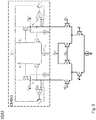
- Fig. 2 shows a second embodiment of a variable gain amplifier VGA2.
- the present embodiment differs from VGA1 shown in Fig. 1 mainly in utilizing a transimpedance amplifier as a load instead of the resistive loads, and consequently a required alteration in the common-mode bias serve stage CMBS2.
- the differential load stage CMBS2 comprises respective transimpedance amplifiers in two half-circuits receiving the supply voltage. Each of the transimpedance amplifier receives the differential pair of current components via a respective one of the half-circuits.
- the half-circuits of the common-mode bias servo stage CMBS2 each comprise a resistively loaded common emitter amplifier having a load resistor R C connected to the supply voltage input Vcc1, and a feedback resistor R F connected between a control base of the common emitter amplifier and the respective differential signal output node Out n , Out p for providing the DC bias voltage.
- Each half-circuit further comprises a buffer transistor Q7, Q8 connected in parallel to the load resistance R C and connected between the supply voltage input and the respective differential signal output node Out n , Out p .
- Using the buffer transistors Q7 and Q8 achieves a buffering of the load resistance R C from a driven capacitive load, and so increases the achieved bandwidth. It also steps down the DC operating point to bias the input transistors bases of Q5 and Q6 correctly.
- a first one supplies current to the VGA gm stage (Q1, Q2) and to the current commuting cascade devices (Q1-Q4).
- the second current source serves to bias the input transistors (Q5, Q6) of the transimpedance amplifiers.
- the current sources connected to output voltage signal nodes Out n , Out p serve for biasing the emitter follower transistors Q7 and Q8. The choice of the current values depends on the targeted specifications.
- voltage supply circuitry (not shown) provides the VGA supply voltage input and the voltage supply input with an identical voltage amount Vcc1, such that the VGA supply voltage amount provided to the current commuting stage and the supply voltage amount provided to the differential load stage are identical.
- the transimpedance amplifier thus acts as the load for VGA2.
- Transistors Q1 and Q4 deliver the current to the transimpedance amplifier to be multiplied by the feedback resistor R F and so convert it to a voltage signal at the respective differential signal output nodes Out n , Out p .
- Fig. 3 shows a third embodiment of a variable gain amplifier VGA3.
- the present embodiment differs from VGA2 shown in Fig. 2 only in providing the reference voltage in the common-mode bias servo stage CMBS3, in that a dedicated on-chip reference voltage supply is provided which is configured to provide the reference voltage V REF only to the common-mode bias servo stage.
- V BE is the minimum threshold voltage across the base-emitter junction for the HBT (bjt) transistor to be in the active forward operation. This approach can be utilized as a DC offset cancellation loop.
- Fig. 4 shows a schematic diagram of a wireless homodyne receiver.
- the variable gain amplifier (VGA) is an important building block in integrated direct conversion receivers for wireless and wireline communication systems.
- the homodyne receiver has a radio frequency input unit such as an antenna for providing a radio frequency signal to a low-noise amplifier LNA.
- a frequency converter receives an amplified radio frequency signal from the low-noise amplifier LNA and a local oscillation signal LO converts the amplified radio frequency signal into a baseband signal.
- An amplifier stage comprising two variable gain amplifiers of the type described by any of the embodiments VGA1 to VGA3 receives the base band signal and provides an amplified base band signal.
- Fig. 5 shows a schematic diagram of a wireless photonics receiver having a cascade of variable gain amplifiers according to one of the first to third embodiments.
- Long-haul fiber optic communication systems require conversion of a received optical signal to electric current through a photodetector which is then converted to a voltage signal via an amplifier stage comprising cascaded VGA stages to reach the required voltage swing.
- the photonics receiver of Fig. 5 comprises a photodetector unit for receiving a modulated photonic signal and converting it into a modulated electric signal.
- An amplifier stage comprising at least one variable gain amplifier that receives the modulated electronic signal and is configured to provide an amplified modulated signal by first converting to a voltage signal via a transimpedance amplifier (TIA), which is followed by two variable gain amplifiers in accordance with the present invention or one of its embodiments.
- TIA transimpedance amplifier
- the solution presented avoids varying DC common mode voltage at different gain stages, and guarantees a fixed input DC common mode voltage for the following stage. It also allows much more flexibility for the design of the VGA gain because the feedback resistance and the bias current can be optimized for gain and linearity independently from the DC levels and bias conditions, which is helpful for optimized designs.
Landscapes
- Engineering & Computer Science (AREA)
- Power Engineering (AREA)
- Microelectronics & Electronic Packaging (AREA)
- Amplifiers (AREA)
Abstract
Description
- The present invention relates to a variable gain amplifier for amplifying a differential pair of input voltage signals.
- A variable gain amplifier (VGA) is an important building block in integrated direct conversion receivers (homodyne receivers) for wireless and wireline communication systems. In wireless communication systems the RF signal is down-converted to baseband and then amplified via cascaded VGA stages to reach the required full scale voltage swing needed by an analog to digital converter (ADC). In wireline communication systems, such as long-haul fiber optic communication systems, the received optical signal is converted to an electric current through a photo diode (PD). The electric current is then converted to voltage signal via a transimpedance amplifier (TIA), and later amplified by cascaded VGA stages to reach a required voltage swing.
- VGAs based on the Gilbert cell are well known. Another commonly used VGA topology comprises a main trans-conductance stage delivering current into a current commuting cascode stage. By controlling the current steered into a load resistance using the control voltages, the gain of the VGA is controlled. This topology shows better performance compared to a Gilbert cell based VGA in terms of bandwidth uniformity across different gain states. It also has a better bandwidth due to lower load capacitance compared to the Gilbert cell based VGA.
- A general problem with cascaded VGA stages for amplifying a differential pair of input voltage signals is a direct coupling between the VGA stages, which leads to shared common mode voltage levels. This in turn puts limitations on design parameters of the VGA and leads to suboptimal designs. In some cases, due to the limitations in the common mode voltage levels in between the VGA stages, additional VGA stages are required in direct conversion receivers to achieve the required gain.
- An output common mode voltage increases in particular at lower gain states. This effect leads to a degraded linearity at the lower gain states. Furthermore, headroom problems arise across process variations. In addition, the higher output common mode at lower gain states limits the achievable voltage swing which contributes also in having worse linearity.
- According to the present invention, a variable gain amplifier for amplifying a differential pair of input voltage signals comprises
- a control input for receiving a differential pair of gain control voltage signals;
- a differential signal input for receiving a differential pair of input voltage signals;
- a current commuting stage receiving the pair of input voltage signals and the gain control voltage, and comprising a pair of cascode circuits for providing a differential pair of current components of respective current amounts that depend on the respective input voltage signal and on the received gain control voltage;
- a differential load stage receiving the current components and having respective resistive loads of a respective load resistance amount; and
- a differential signal output for providing a differential pair of output voltage signals having respective output voltage amounts that depend on the respective current amounts and on the load resistance amounts; wherein the variable gain amplifier further comprises
- a common-mode bias servo stage that receives a reference voltage of a reference voltage amount and the differential pair of output voltage signals, and that comprises a pair of closed loop differential amplifiers, each configured to generate a respective DC bias voltage of a DC bias voltage amount depending on a difference between the respective output voltage amount and the reference voltage amount, and each feeding the respective generated DC bias voltage back to a respective differential signal output node.
- The variable gain amplifier of the present invention, hereinafter also referred to in short as VGA, is based on the recognition that conventional approaches to reducing or avoiding common mode voltages raise new problems. In particular, for avoiding problems created by common mode voltages, either the resistive load or a bias current could be increased so as to increase the gain of the VGA, which in turn would lead to a lower output common mode voltage. However, this would add constraints on the design and in the outcome would lead to suboptimal designs. To overcome such limitations, a new VGA design in accordance with
claim 1 is proposed. - The VGA of the present invention includes a common-mode bias servo stage that receives a reference voltage of a reference voltage amount and the differential pair of output voltage signals, and that comprises a pair of closed loop differential amplifiers, each configured to generate a respective DC bias voltage of a DC bias voltage amount depending on a difference between the respective output voltage amount and the reference voltage amount, and each feeding the respective generated DC bias voltage back to the respective differential signal output node.
- This way, a feedback loop is implemented which acts as a biasing network for the VGA. This regulates the output DC common mode voltage of the VGA. By introducing a closed loop differential amplifier for sensing the DC voltage component of the output voltage and comparing it to a reference voltage, an output of the differential amplifier can be used as a DC bias voltage, which is fed back to the respective differential signal output node. By proper selection of the reference voltage in operation of the VGA, this loop can achieve that a common mode output current through the resistive load is greatly reduced or even fully eliminated, and thus only AC signal components flow through the resistive loads of the VGA.
- In the following, embodiments of the variable gain amplifier circuit of the present invention will be described. The additional features of these embodiments can be combined with each other to form further embodiments, unless explicitly specified as forming alternatives.
- Suitably, the VGA comprises a VGA supply voltage input for receiving a VGA supply voltage (Vcc2) of a VGA supply voltage amount. The VGA voltage supply input is suitably connected to a voltage supply unit that is in one embodiment arranged on-chip, together with the VGA.
- While the voltage supply unit is provided as a part of the VGA in one embodiment, this is not a requirement. In other embodiments, any required supply voltage is received from a separate device that is not a part of the claimed VGA. Rather, in such embodiments, the voltage supply unit forms a part of a circuit environment to which the VGA can be connected for operation in a given application case.
- In preferred embodiments, the respective closed loop differential amplifiers each comprise an operational amplifier having a non-inverting input receiving the reference voltage and an inverting input receiving a respective output voltage signal of the output voltage signal pair. The respective operational amplifier is configured to generate and provide a current control signal that depends on a difference between the reference voltage and the output voltage signal. The current control signal is fed to a respective voltage controlled current source.
- In some embodiments, the reference voltage amount equals the VGA supply voltage amount. This can be achieved by providing the VGA supply voltage (Vcc2) to both the VGA supply voltage input and to the reference voltage input. However, it is also possible to provide the reference voltage from a separate reference voltage supply unit. By using voltage supply circuitry configured to provide the reference voltage with a reference voltage amount that is equal to the supply VGA voltage amount, it can be achieved that the DC current component of the VGA is completely delivered by the voltage controlled current source. Thus, as desired, it is achieved that only the AC signal flows through the VGA resistive load for amplification.
- The voltage controlled current source is implemented in some embodiments by a PMOS transistor connected in common source mode between the voltage supply input and the respective signal output node of the differential signal output for providing the DC bias voltage. Other types of voltage-controlled current sources can be used, such as for instance a bipolar pnp transistor instead of the PMOS transistor.
- In a similar way as described for the VGA supply voltage input, also the voltage supply input used for operating the voltage controlled current source can be suitably connected to voltage supply circuitry, which in one embodiment comprises an on-chip voltage supply. In some embodiments of the VGA, as will be explained further below, the voltage amounts to be provided via the VGA supply voltage input and via the voltage supply input are different from each other, in order to advantageously achieve an optimum suppression of common mode DC current through the resistive load. In these cases, depending on the received amount of supply voltage or VGA supply voltage, the voltage supply circuitry comprises a suitable voltage conversion circuit in at least one of the voltage-supply branches supplying the VGA.
- More specifically, in embodiments using a PMOS transistor for the voltage controlled current source in combination with using a differential load stage consisting of respective resistive loads in the form of resistors in the two parallel half-circuits receiving the supply voltage, the voltage supply circuitry is preferably configured to provide the supply voltage with a supply voltage amount that equals a sum of the VGA supply voltage amount and a minimum voltage amount Vdsat required to keep a the PMOS transistor in saturation. In short, this requirement can be expressed as Vccl= Vcc2+Vdsat, wherein Vcc1 is the supply voltage amount, and Vcc2 is the VGA supply voltage amount. Vdsat depends on technology parameters and a transistor sizing. So the amount of Vdsat can be adapted in the VGA circuit design by suitable selection or dimensioning of the mentioned parameters.
- In preferred embodiments, the differential load stage comprises respective resistive loads of an identical load resistance amount in two parallel half-circuits receiving the supply voltage.
- In one variant of this kind of embodiments, the differential load stage comprises or consists of identical resistors in each of the two parallel half-circuits, both half-circuits receiving the supply voltage.
- In another variant of this kind of embodiment, the differential load stage comprises respective transimpedance amplifiers in the two parallel half-circuits receiving the supply voltage. The transimpedance amplifiers are preferably identical. The differential load stage of variant is preferably configured to receive the current components from the current commuting stage via the respective half-circuits, which each comprise a resistively loaded common emitter amplifier (RC, Q5; RC, Q6) having a load resistor (RC) connected to the supply voltage input, and which each comprise a feedback resistor (RF) connected between a control base node of the amplifier and the respective differential signal output node for providing the DC bias voltage. Sensing and biasing operation is thus performed across the feedback resistor (RF). The transimpedance amplifier can thus be described in short as an amplifier with a resistive feedback (RF) having a transfer function that can roughly be given as Vout = Iin x RF, where Vout is an output voltage of the transimpedance amplifier, Iin is the input current provided by the current commuting stage, and RF is the feedback resistance.
- In embodiments comprising respective transimpedance amplifiers in the two half-circuits receiving the supply voltage, the voltage supply circuitry is preferably configured to provide the supply voltage with a supply voltage amount (Vcc1) that equals the VGA supply voltage amount (Vcc2), i.e. Vcc1 = Vcc2. The supply voltage, and thus the VGA supply voltage is to be provided in these embodiments with an amount high enough to keep all transistors in active forward operation.
- In one embodiment, a dedicated on-chip reference voltage supply is provided which is configured to provide only the reference voltage only to the common-mode bias servo stage.
- In some embodiments, the transimpedance amplifier is configured to receive the differential pair of current components via the respective half-circuits, which each comprise a resistively loaded common emitter amplifier having a load resistor connected to the supply voltage input and a feedback resistor connected between a control base of the amplifier and the respective differential signal output for providing the DC bias voltage.
- In these embodiments, each half-circuit further preferably comprises a buffer transistor connected in parallel to the load resistance RC and connected between the supply voltage input and the respective differential signal output node. It is preferably implemented as an emitter follower buffer and achieves an enhancement of the bandwidth and a step down of the DC voltage in the feedback in order to bias the input of the transimpedance amplifier.
- In one embodiment, a dedicated on-chip reference voltage supply is provided which is configured to provide the reference voltage only to the common-mode bias servo stage.
- The VGA of the present invention can be used in many application context. According to a first exemplary application aspect of the present invention, a direct conversion receiver is provided, comprising
- a radio frequency input unit providing a radio frequency signal to a first amplifier,
- a frequency converter that receives an amplified radio frequency signal from the first amplifier and a local oscillation signal and that is configured to convert the amplified radio frequency signal into a baseband signal, and
- an amplifier stage comprising at least one second variable gain amplifier that receives the base band signal and provides an amplified base band signal, wherein
- the at least one second variable gain amplifier is in accordance with the present invention or one of its embodiments.
- In this application example, the variable gain amplifier is an important building block for a wireless communication system. In a homodyne or direct-conversion receiver, the RF signal is down-converted to baseband and then amplified via cascaded VGA stages to reach the required full scale voltage swing needed by an analog to digital converter (ADC).
- A second application aspect is formed by a photonic receiver, comprising
- a photodetector unit for receiving a modulated photonic signal and converting it into a modulated electric signal, and
- an amplifier stage comprising at least one variable gain amplifier that receives the modulated electronic signal and is configured to provide an amplified modulated signal, wherein
- the variable gain amplifier is in accordance with the present invention or one of its embodiments.
- Long-haul fiber optic communication systems require conversion of a received optical signal to electric current through a photodetector which is then converted to a voltage signal via an amplifier stage comprising cascaded VGA stages to reach the required voltage swing.
- In both application contexts, limitations of the prior art on the design parameters of the VGA, leading to suboptimal designs, can be avoided. Also the number of VGA stages can be kept small since there are no limitations in the common mode voltage levels in between the stages.
- Further embodiments of the VGA will be described in the following with reference to the enclosed drawings.
-
Fig. 1 shows a first embodiment of a variable gain amplifier; -
Fig. 2 shows a second embodiment of a variable gain amplifier; -
Fig. 3 shows a third embodiment of a variable gain amplifier; -
Fig. 4 shows a schematic diagram of a wireless homodyne receiver having a cascade of variable gain amplifiers according to one of the first to third embodiments; -
Fig. 5 shows a schematic diagram of a wireless photonics receiver having a cascade of variable gain amplifiers according to one of the first to third embodiments; -
Fig. 1 shows a first embodiment of a variable gain amplifier VGA1. For brevity, the following description will refer to variable gain amplifier VGA1 ofFig. 1 as VGA1 only. For amplifying a differential pair of input voltage signals, VGA1 comprises two half-circuits, each receiving a VGA supply voltage Vcc2 with an identical voltage amount. VGA1 also comprises a VGA supply voltage input for receiving the VGA supply voltage Vcc2. The VGA voltage supply input is connected to a voltage supply unit (not shown) that is suitably, but not necessarily arranged on-chip, together with the VGA. - A respective control input in each half-circuit receives a differential pair of gain control voltage signals VCp and VCn.
- A differential signal input receives an incoming differential pair of input voltage signals Ip and In.
- A current commuting stage comprises a cascode stage. The cascode stage comprising transistors Q1 to Q4 has a pair of cascode circuits Q1, Qn and Q2, Qn in a first half-circuit that receives the input voltage signal IP, and a pair of cascode circuits Q3, Qp and Q4, Qp in the second half-circuit that receives the input voltage signal In. The cascode stage provides a differential pair of current components of respective current amounts that depend on the respective input voltage signal and on the received gain control voltage. The current commuting stage also receives the VGA supply voltage Vcc2.
- A trans-conductance stage is formed by the transistors Qn and Qp and delivers current into the current commuting stage. A bias control allowing an application of a bias voltage Vbias to a bias control transistor Qbias is connected to the trans-conductance stage. However, it is noted that this bias control is optional and can also be omitted. Another embodiment therefore does not comprise the bias control transistor Qbias, but provides a direct connection to ground potential.
- The current components provided by the current commuting stage are provided to a differential load stage that includes respective resistive loads in the form of resistors RL having an identical load resistance amount. The voltage thus generated in each half-circuit by providing the resistors RL with the current components generates a differential pair of output voltage signals Outn, Outp with respective output voltage amounts that depend on the respective current amounts and on the load resistance amounts. So by controlling the current steered into the load resistance RL using the control voltages VCn and VCp, the gain of VGA1 is controlled.
- A common-mode bias servo stage CMBS1 (encircled by a dashed line) receives a reference voltage of a reference voltage amount that in the present embodiment is identical to the VGA supply voltage Vcc2. It also receives the differential pair of output voltage signals Outn and Outp. The common-mode bias servo stage CMBS1 comprises a pair of closed loop differential amplifiers using operational amplifiers labelled OpAmp in
Fig. 1 , each being configured to generate a respective DC bias voltage of a DC bias voltage amount depending on a difference between the received respective output voltage amount and the received reference voltage amount (here: Vcc2), and each feeding the respective generated DC bias voltage back to the respective differential signal output node. To provide the DC bias voltage, the output voltage of the respective operational amplifier provides its output as a respective current control signal that is fed to a respective voltage controlled current source. The voltage controlled current source is a PMOS transistor P1, P2 connected in common source mode between a voltage supply input providing a supply voltage Vcc1 and the respective differential signal output node Outn, Outp of the differential signal output. The supply voltage Vcc1 suitably has a supply voltage amount that equals a sum of the VGA supply voltage amount Vcc2 and a minimum voltage amount Vdsat required to keep the PMOS transistor in saturation. This can be expressed in short as Vcc1 = Vcc2 + Vdsat. Vdsat depends on technology parameters and a transistor sizing. So the amount of Vdsat can be adapted in the VGA circuit design by suitable selection or dimensioning of the mentioned parameters. - Thus, the common-mode bias servo stage CMBS1 advantageously provides a feedback loop which acts as a biasing network for the variable gain amplifier VGA1. This regulates an output DC common mode voltage of VGA1 by sensing the DC voltage and comparing it to a reference voltage (here: Vcc2) using the operational amplifiers OpAmp, with the output of the OpAmps controlling the gate of a respective PMOS device P1,P2, which in turn act as a DC current source for the variable gain amplifier VGA1. By setting the reference voltage equal to the supply of VGA1 (namely, Vcc2), this loop achieves that the DC current of VGA1 is delivered by the PMOS device P1, P2 and only the AC signal is to flow through the resistive load RL of VGA1.
-
Fig. 2 shows a second embodiment of a variable gain amplifier VGA2. The present embodiment differs from VGA1 shown inFig. 1 mainly in utilizing a transimpedance amplifier as a load instead of the resistive loads, and consequently a required alteration in the common-mode bias serve stage CMBS2. - The following description will focus on these differences.
- The differential load stage CMBS2 comprises respective transimpedance amplifiers in two half-circuits receiving the supply voltage. Each of the transimpedance amplifier receives the differential pair of current components via a respective one of the half-circuits. The half-circuits of the common-mode bias servo stage CMBS2 each comprise a resistively loaded common emitter amplifier having a load resistor RC connected to the supply voltage input Vcc1, and a feedback resistor RF connected between a control base of the common emitter amplifier and the respective differential signal output node Outn, Outp for providing the DC bias voltage. Each half-circuit further comprises a buffer transistor Q7, Q8 connected in parallel to the load resistance RC and connected between the supply voltage input and the respective differential signal output node Outn, Outp. Using the buffer transistors Q7 and Q8 achieves a buffering of the load resistance RC from a driven capacitive load, and so increases the achieved bandwidth. It also steps down the DC operating point to bias the input transistors bases of Q5 and Q6 correctly.
- There are four current sources. A first one supplies current to the VGA gm stage (Q1, Q2) and to the current commuting cascade devices (Q1-Q4). The second current source serves to bias the input transistors (Q5, Q6) of the transimpedance amplifiers. The current sources connected to output voltage signal nodes Outn, Outp serve for biasing the emitter follower transistors Q7 and Q8. The choice of the current values depends on the targeted specifications.
- For operating the embodiment of
Fig. 2 , voltage supply circuitry (not shown) provides the VGA supply voltage input and the voltage supply input with an identical voltage amount Vcc1, such that the VGA supply voltage amount provided to the current commuting stage and the supply voltage amount provided to the differential load stage are identical. - In effect, the transimpedance amplifiers thus receive an input current signal in the form of the differential pair of current components, and provide a voltage output signal. They basically can be described as amplifiers with resistive feedback formed by the feedback resistor (RF). So a transfer function is basically as Vout = Iin x RF, where Vout is an output voltage of the transimpedance amplifier, Iin is the input current provided by the current commuting stage, and RF is the feedback resistance. The transimpedance amplifier thus acts as the load for VGA2. Transistors Q1 and Q4 deliver the current to the transimpedance amplifier to be multiplied by the feedback resistor RF and so convert it to a voltage signal at the respective differential signal output nodes Outn, Outp.
- In comparison with the embodiment of
Fig. 1 , by replacing the resistive load with a transimpedance amplifier, the common mode voltage regulation in VGA2 will take place at a different node from the dominant pole, and so the bandwidth degradation will be minimal. Bandwidth degradation can thus be avoided, because of an extra capacitance at the output node, which is mostly the dominant pole. The common mode voltage problem is thus solved without affecting the VGA bandwidth. -
Fig. 3 shows a third embodiment of a variable gain amplifier VGA3. The present embodiment differs from VGA2 shown inFig. 2 only in providing the reference voltage in the common-mode bias servo stage CMBS3, in that a dedicated on-chip reference voltage supply is provided which is configured to provide the reference voltage VREF only to the common-mode bias servo stage. The reference voltage is suitable selected as VREF = (Vcc1-IbiasRC - VBE). Here, VBE is the minimum threshold voltage across the base-emitter junction for the HBT (bjt) transistor to be in the active forward operation. This approach can be utilized as a DC offset cancellation loop. -
Fig. 4 shows a schematic diagram of a wireless homodyne receiver. The variable gain amplifier (VGA) is an important building block in integrated direct conversion receivers for wireless and wireline communication systems. - The homodyne receiver has a radio frequency input unit such as an antenna for providing a radio frequency signal to a low-noise amplifier LNA. A frequency converter receives an amplified radio frequency signal from the low-noise amplifier LNA and a local oscillation signal LO converts the amplified radio frequency signal into a baseband signal. An amplifier stage comprising two variable gain amplifiers of the type described by any of the embodiments VGA1 to VGA3 receives the base band signal and provides an amplified base band signal.
-
Fig. 5 shows a schematic diagram of a wireless photonics receiver having a cascade of variable gain amplifiers according to one of the first to third embodiments. Long-haul fiber optic communication systems require conversion of a received optical signal to electric current through a photodetector which is then converted to a voltage signal via an amplifier stage comprising cascaded VGA stages to reach the required voltage swing. The photonics receiver ofFig. 5 comprises a photodetector unit for receiving a modulated photonic signal and converting it into a modulated electric signal. An amplifier stage comprising at least one variable gain amplifier that receives the modulated electronic signal and is configured to provide an amplified modulated signal by first converting to a voltage signal via a transimpedance amplifier (TIA), which is followed by two variable gain amplifiers in accordance with the present invention or one of its embodiments. - In summary, thus, the solution presented avoids varying DC common mode voltage at different gain stages, and guarantees a fixed input DC common mode voltage for the following stage. It also allows much more flexibility for the design of the VGA gain because the feedback resistance and the bias current can be optimized for gain and linearity independently from the DC levels and bias conditions, which is helpful for optimized designs.
Claims (13)
- A variable gain amplifier for amplifying a differential pair of input voltage signals, comprising- a control input for receiving a differential pair of gain control voltage signals;- a differential signal input for receiving a differential pair of input voltage signals;- a current commuting stage receiving the pair of input voltage signals and the gain control voltage, and comprising a pair of cascode circuits for providing a differential pair of current components of respective current amounts that depend on the respective input voltage signal and on the received gain control voltage;- a differential load stage receiving the current components and having respective resistive loads of a respective load resistance amount for generating a differential pair of output voltage signals having respective output voltage amounts that depend on the respective current amounts and on the load resistance amounts; and- a differential signal output having respective differential signal output nodes for providing the differential pair of output voltage signals; wherein the variable gain amplifier further comprises- a common-mode bias servo stage that receives a reference voltage of a reference voltage amount and the differential pair of output voltage signals, and that comprises a pair of closed loop differential amplifiers, each configured to generate a respective DC bias voltage of a DC bias voltage amount depending on a difference between the respective output voltage amount and the reference voltage amount, and each feeding the respective generated DC bias voltage back to the respective differential signal output node.
- The variable gain amplifier circuit of claim 1, wherein- the respective closed loop differential amplifiers of the common-mode bias servo stage each comprise an operational amplifier having a non-inverting input receiving the reference voltage and an inverting input receiving a respective output voltage signal of the output voltage signal pair; and wherein- the respective operational amplifier generates and provides a respective current control signal that is fed to a respective voltage controlled current source that is connected with a voltage supply input to receive a supply voltage and with the respective signal output node of the differential signal output.
- The variable gain amplifier circuit of claim 1 or 2, comprising voltage supply circuitry for supplying the reference voltage input and the VGA supply voltage with an identical voltage amount, such that the input reference voltage amount equals the VGA supply voltage amount.
- The variable gain amplifier circuit of claim 2 or 3, wherein the voltage controlled current source is a PMOS transistor connected in common source mode between the voltage supply input and the respective differential signal output node of the differential signal output.
- The variable gain amplifier of at least one of the preceding claims, wherein the differential load stage comprises respective resistive loads of an identical load resistance amount in two half-circuits receiving the supply voltage.
- The variable gain amplifier of claims 2, 4 and 5, comprising voltage supply circuitry providing the voltage supply input with the supply voltage of a supply voltage amount that equals a sum of the VGA supply voltage amount and a minimum voltage amount Vdsat required to keep the PMOS transistor in saturation.
- The variable gain amplifier of at least one of the claims 2 to 5, wherein the differential load stage comprises respective transimpedance amplifiers in two half-circuits receiving the supply voltage.
- The variable gain amplifier of claim 7, comprising voltage supply circuitry configured to provide the VGA supply voltage input and the voltage supply input with an identical voltage amount, such that the VGA supply voltage amount provided to the current commuting stage and the supply voltage amount provided to the differential load stage are identical.
- The variable gain amplifier of claim 7 or 8, wherein the transimpedance amplifier is configured to receive the differential pair of current components via the respective half-circuits, which each comprise a resistively loaded common emitter amplifier (RC, Q5; RC, Q6) having a load resistor (RC) connected to the supply voltage input and a feedback resistor (RF) connected between a control base of the amplifier and the respective differential signal output for providing the DC bias voltage.
- The variable gain amplifier of claim 9, wherein each half-circuit further comprises a buffer transistor connected in parallel to the load resistance RC and connected between the supply voltage input and the respective differential signal output node.
- The variable gain amplifier of one of the claims 7 to 10, comprising a dedicated on-chip reference voltage supply which is configured to provide the reference voltage only to the common-mode bias servo stage.
- A direct conversion receiver comprising- a radio frequency input unit providing a radio frequency signal to a first amplifier,- a frequency converter that receives an amplified radio frequency signal from the first amplifier and a local oscillation signal and that is configured to convert the amplified radio frequency signal into a baseband signal, and- an amplifier stage comprising at least one second variable gain amplifier that receives the base band signal and provides an amplified base band signal, wherein- the first variable gain amplifier and the at least one second variable gain amplifier is in accordance with at least one of the preceding claims.
- A photonic receiver comprising- a photodetector unit for receiving a modulated photonic signal and converting it into a modulated electric signal, and- an amplifier stage comprising at least one variable gain amplifier that receives the modulated electronic signal and is configured to provide an amplified modulated signal, wherein- the variable gain amplifier is in accordance with at least one of the preceding claims.
Priority Applications (2)
| Application Number | Priority Date | Filing Date | Title |
|---|---|---|---|
| EP17209770.1A EP3503389B1 (en) | 2017-12-21 | 2017-12-21 | Output common mode voltage regulated variable gain amplifier |
| PCT/EP2018/086694 WO2019122377A1 (en) | 2017-12-21 | 2018-12-21 | Output common mode voltage regulated variable gain amplifier |
Applications Claiming Priority (1)
| Application Number | Priority Date | Filing Date | Title |
|---|---|---|---|
| EP17209770.1A EP3503389B1 (en) | 2017-12-21 | 2017-12-21 | Output common mode voltage regulated variable gain amplifier |
Publications (2)
| Publication Number | Publication Date |
|---|---|
| EP3503389A1 true EP3503389A1 (en) | 2019-06-26 |
| EP3503389B1 EP3503389B1 (en) | 2024-03-13 |
Family
ID=60942853
Family Applications (1)
| Application Number | Title | Priority Date | Filing Date |
|---|---|---|---|
| EP17209770.1A Active EP3503389B1 (en) | 2017-12-21 | 2017-12-21 | Output common mode voltage regulated variable gain amplifier |
Country Status (2)
| Country | Link |
|---|---|
| EP (1) | EP3503389B1 (en) |
| WO (1) | WO2019122377A1 (en) |
Cited By (1)
| Publication number | Priority date | Publication date | Assignee | Title |
|---|---|---|---|---|
| CN114866041A (en) * | 2022-04-28 | 2022-08-05 | 西安交通大学 | DC offset cancellation circuit and method |
Families Citing this family (2)
| Publication number | Priority date | Publication date | Assignee | Title |
|---|---|---|---|---|
| US11687107B2 (en) * | 2020-11-09 | 2023-06-27 | Cirrus Logic, Inc. | Voltage regulators |
| CN116545399A (en) * | 2023-05-30 | 2023-08-04 | 深圳市傲科光电子有限公司 | A variable gain amplifier and communication circuit |
Citations (4)
| Publication number | Priority date | Publication date | Assignee | Title |
|---|---|---|---|---|
| US5578964A (en) * | 1994-04-26 | 1996-11-26 | Korea Telecommunication Authority | CMOS differential operational amplifier |
| US6316996B1 (en) * | 1999-10-25 | 2001-11-13 | Nokia Mobile Phones, Ltd. | Adjustable AC load structure |
| US20030085764A1 (en) * | 2001-10-25 | 2003-05-08 | Connell Lawrence E. | Variable gain amplifier with autobiasing supply regulation |
| US20030214356A1 (en) * | 2002-05-16 | 2003-11-20 | Cowley Nicholas Paul | Amplifier and radio frequency tuner |
Family Cites Families (3)
| Publication number | Priority date | Publication date | Assignee | Title |
|---|---|---|---|---|
| US3684974A (en) * | 1968-01-29 | 1972-08-15 | Motorola Inc | Automatic gain control rf-if amplifier |
| TWI378640B (en) * | 2009-10-23 | 2012-12-01 | Sunplus Technology Co Ltd | Variable-gain low noise amplifier |
| EP3236585B1 (en) * | 2016-04-22 | 2020-12-23 | Goodix Technology (HK) Company Limited | Amplifiers |
-
2017
- 2017-12-21 EP EP17209770.1A patent/EP3503389B1/en active Active
-
2018
- 2018-12-21 WO PCT/EP2018/086694 patent/WO2019122377A1/en not_active Ceased
Patent Citations (4)
| Publication number | Priority date | Publication date | Assignee | Title |
|---|---|---|---|---|
| US5578964A (en) * | 1994-04-26 | 1996-11-26 | Korea Telecommunication Authority | CMOS differential operational amplifier |
| US6316996B1 (en) * | 1999-10-25 | 2001-11-13 | Nokia Mobile Phones, Ltd. | Adjustable AC load structure |
| US20030085764A1 (en) * | 2001-10-25 | 2003-05-08 | Connell Lawrence E. | Variable gain amplifier with autobiasing supply regulation |
| US20030214356A1 (en) * | 2002-05-16 | 2003-11-20 | Cowley Nicholas Paul | Amplifier and radio frequency tuner |
Cited By (1)
| Publication number | Priority date | Publication date | Assignee | Title |
|---|---|---|---|---|
| CN114866041A (en) * | 2022-04-28 | 2022-08-05 | 西安交通大学 | DC offset cancellation circuit and method |
Also Published As
| Publication number | Publication date |
|---|---|
| EP3503389B1 (en) | 2024-03-13 |
| WO2019122377A1 (en) | 2019-06-27 |
Similar Documents
| Publication | Publication Date | Title |
|---|---|---|
| US9716470B2 (en) | Apparatus and methods for compensating an operational amplifier | |
| US6049251A (en) | Wide-dynamic-range variable-gain amplifier | |
| US8970301B2 (en) | Method for low power low noise input bias current compensation | |
| US11990879B2 (en) | Fully-differential amplifier with input common-mode voltage control | |
| US20130135054A1 (en) | Trans-impedance amplifier with enhanced dynamic range but invariable input impedance | |
| US10326416B2 (en) | Amplifier | |
| US8324956B2 (en) | Flexible low noise, high linearity, high frequency, low power, fully differential mixer and class AB post-mixer amplifier system for SDR applications | |
| EP4387094A1 (en) | Dc voltage regulation and tia with input-output dc voltage control | |
| EP3503389B1 (en) | Output common mode voltage regulated variable gain amplifier | |
| JP6107103B2 (en) | Amplifier and optical receiver | |
| JP2009260972A (en) | Variable gain rf amplifier | |
| US12316281B2 (en) | Reception circuit for optical communication | |
| JP6389144B2 (en) | Current detection circuit | |
| US7319220B2 (en) | Trans-impedance amplifier with offset current | |
| US8816772B2 (en) | Differential amplifier with function of variable gain and optical receiver implemented with the same | |
| US6664912B1 (en) | Preamplifier with improved CMRR and temperature stability and associated amplification method | |
| JP4896819B2 (en) | High frequency signal detection circuit | |
| US8179198B2 (en) | Variable gain amplifier having automatic power consumption optimization | |
| US20240214077A1 (en) | Receiver circuit and optical receiver circuit | |
| CN219592380U (en) | Variable gain amplifier and communication circuit | |
| CN110572133B (en) | Fully differential transimpedance amplifier circuit and communication device | |
| GB2371697A (en) | Scaled current sinks for a cross-coupled low-intermodulation RF amplifier | |
| US5917376A (en) | Circuit and technique for compensating high gain amplifier without compensation capacitors | |
| CN116545399A (en) | A variable gain amplifier and communication circuit | |
| EP3439175B1 (en) | Input current adjustment for fully differential transimpedance amplifiers |
Legal Events
| Date | Code | Title | Description |
|---|---|---|---|
| PUAI | Public reference made under article 153(3) epc to a published international application that has entered the european phase |
Free format text: ORIGINAL CODE: 0009012 |
|
| STAA | Information on the status of an ep patent application or granted ep patent |
Free format text: STATUS: THE APPLICATION HAS BEEN PUBLISHED |
|
| AK | Designated contracting states |
Kind code of ref document: A1 Designated state(s): AL AT BE BG CH CY CZ DE DK EE ES FI FR GB GR HR HU IE IS IT LI LT LU LV MC MK MT NL NO PL PT RO RS SE SI SK SM TR |
|
| AX | Request for extension of the european patent |
Extension state: BA ME |
|
| STAA | Information on the status of an ep patent application or granted ep patent |
Free format text: STATUS: REQUEST FOR EXAMINATION WAS MADE |
|
| 17P | Request for examination filed |
Effective date: 20200102 |
|
| RBV | Designated contracting states (corrected) |
Designated state(s): AL AT BE BG CH CY CZ DE DK EE ES FI FR GB GR HR HU IE IS IT LI LT LU LV MC MK MT NL NO PL PT RO RS SE SI SK SM TR |
|
| STAA | Information on the status of an ep patent application or granted ep patent |
Free format text: STATUS: EXAMINATION IS IN PROGRESS |
|
| 17Q | First examination report despatched |
Effective date: 20211117 |
|
| GRAP | Despatch of communication of intention to grant a patent |
Free format text: ORIGINAL CODE: EPIDOSNIGR1 |
|
| STAA | Information on the status of an ep patent application or granted ep patent |
Free format text: STATUS: GRANT OF PATENT IS INTENDED |
|
| RIC1 | Information provided on ipc code assigned before grant |
Ipc: H03F 3/195 20060101ALI20231107BHEP Ipc: H03F 3/08 20060101ALI20231107BHEP Ipc: H03F 1/48 20060101ALI20231107BHEP Ipc: H03F 3/45 20060101ALI20231107BHEP Ipc: H03G 1/00 20060101AFI20231107BHEP |
|
| INTG | Intention to grant announced |
Effective date: 20231121 |
|
| GRAS | Grant fee paid |
Free format text: ORIGINAL CODE: EPIDOSNIGR3 |
|
| GRAA | (expected) grant |
Free format text: ORIGINAL CODE: 0009210 |
|
| STAA | Information on the status of an ep patent application or granted ep patent |
Free format text: STATUS: THE PATENT HAS BEEN GRANTED |
|
| AK | Designated contracting states |
Kind code of ref document: B1 Designated state(s): AL AT BE BG CH CY CZ DE DK EE ES FI FR GB GR HR HU IE IS IT LI LT LU LV MC MK MT NL NO PL PT RO RS SE SI SK SM TR |
|
| REG | Reference to a national code |
Ref country code: GB Ref legal event code: FG4D |
|
| REG | Reference to a national code |
Ref country code: CH Ref legal event code: EP |
|
| REG | Reference to a national code |
Ref country code: DE Ref legal event code: R096 Ref document number: 602017079937 Country of ref document: DE |
|
| REG | Reference to a national code |
Ref country code: IE Ref legal event code: FG4D |
|
| PG25 | Lapsed in a contracting state [announced via postgrant information from national office to epo] |
Ref country code: LT Free format text: LAPSE BECAUSE OF FAILURE TO SUBMIT A TRANSLATION OF THE DESCRIPTION OR TO PAY THE FEE WITHIN THE PRESCRIBED TIME-LIMIT Effective date: 20240313 |
|
| REG | Reference to a national code |
Ref country code: LT Ref legal event code: MG9D |
|
| PG25 | Lapsed in a contracting state [announced via postgrant information from national office to epo] |
Ref country code: GR Free format text: LAPSE BECAUSE OF FAILURE TO SUBMIT A TRANSLATION OF THE DESCRIPTION OR TO PAY THE FEE WITHIN THE PRESCRIBED TIME-LIMIT Effective date: 20240614 |
|
| REG | Reference to a national code |
Ref country code: NL Ref legal event code: MP Effective date: 20240313 |
|
| PG25 | Lapsed in a contracting state [announced via postgrant information from national office to epo] |
Ref country code: RS Free format text: LAPSE BECAUSE OF FAILURE TO SUBMIT A TRANSLATION OF THE DESCRIPTION OR TO PAY THE FEE WITHIN THE PRESCRIBED TIME-LIMIT Effective date: 20240613 Ref country code: HR Free format text: LAPSE BECAUSE OF FAILURE TO SUBMIT A TRANSLATION OF THE DESCRIPTION OR TO PAY THE FEE WITHIN THE PRESCRIBED TIME-LIMIT Effective date: 20240313 |
|
| PG25 | Lapsed in a contracting state [announced via postgrant information from national office to epo] |
Ref country code: ES Free format text: LAPSE BECAUSE OF FAILURE TO SUBMIT A TRANSLATION OF THE DESCRIPTION OR TO PAY THE FEE WITHIN THE PRESCRIBED TIME-LIMIT Effective date: 20240313 |
|
| PG25 | Lapsed in a contracting state [announced via postgrant information from national office to epo] |
Ref country code: RS Free format text: LAPSE BECAUSE OF FAILURE TO SUBMIT A TRANSLATION OF THE DESCRIPTION OR TO PAY THE FEE WITHIN THE PRESCRIBED TIME-LIMIT Effective date: 20240613 Ref country code: NO Free format text: LAPSE BECAUSE OF FAILURE TO SUBMIT A TRANSLATION OF THE DESCRIPTION OR TO PAY THE FEE WITHIN THE PRESCRIBED TIME-LIMIT Effective date: 20240613 Ref country code: LT Free format text: LAPSE BECAUSE OF FAILURE TO SUBMIT A TRANSLATION OF THE DESCRIPTION OR TO PAY THE FEE WITHIN THE PRESCRIBED TIME-LIMIT Effective date: 20240313 Ref country code: HR Free format text: LAPSE BECAUSE OF FAILURE TO SUBMIT A TRANSLATION OF THE DESCRIPTION OR TO PAY THE FEE WITHIN THE PRESCRIBED TIME-LIMIT Effective date: 20240313 Ref country code: GR Free format text: LAPSE BECAUSE OF FAILURE TO SUBMIT A TRANSLATION OF THE DESCRIPTION OR TO PAY THE FEE WITHIN THE PRESCRIBED TIME-LIMIT Effective date: 20240614 Ref country code: FI Free format text: LAPSE BECAUSE OF FAILURE TO SUBMIT A TRANSLATION OF THE DESCRIPTION OR TO PAY THE FEE WITHIN THE PRESCRIBED TIME-LIMIT Effective date: 20240313 Ref country code: ES Free format text: LAPSE BECAUSE OF FAILURE TO SUBMIT A TRANSLATION OF THE DESCRIPTION OR TO PAY THE FEE WITHIN THE PRESCRIBED TIME-LIMIT Effective date: 20240313 Ref country code: BG Free format text: LAPSE BECAUSE OF FAILURE TO SUBMIT A TRANSLATION OF THE DESCRIPTION OR TO PAY THE FEE WITHIN THE PRESCRIBED TIME-LIMIT Effective date: 20240313 |
|
| REG | Reference to a national code |
Ref country code: AT Ref legal event code: MK05 Ref document number: 1666707 Country of ref document: AT Kind code of ref document: T Effective date: 20240313 |
|
| PG25 | Lapsed in a contracting state [announced via postgrant information from national office to epo] |
Ref country code: SE Free format text: LAPSE BECAUSE OF FAILURE TO SUBMIT A TRANSLATION OF THE DESCRIPTION OR TO PAY THE FEE WITHIN THE PRESCRIBED TIME-LIMIT Effective date: 20240313 Ref country code: LV Free format text: LAPSE BECAUSE OF FAILURE TO SUBMIT A TRANSLATION OF THE DESCRIPTION OR TO PAY THE FEE WITHIN THE PRESCRIBED TIME-LIMIT Effective date: 20240313 |
|
| PG25 | Lapsed in a contracting state [announced via postgrant information from national office to epo] |
Ref country code: NL Free format text: LAPSE BECAUSE OF FAILURE TO SUBMIT A TRANSLATION OF THE DESCRIPTION OR TO PAY THE FEE WITHIN THE PRESCRIBED TIME-LIMIT Effective date: 20240313 |
|
| PG25 | Lapsed in a contracting state [announced via postgrant information from national office to epo] |
Ref country code: NL Free format text: LAPSE BECAUSE OF FAILURE TO SUBMIT A TRANSLATION OF THE DESCRIPTION OR TO PAY THE FEE WITHIN THE PRESCRIBED TIME-LIMIT Effective date: 20240313 |
|
| PG25 | Lapsed in a contracting state [announced via postgrant information from national office to epo] |
Ref country code: IS Free format text: LAPSE BECAUSE OF FAILURE TO SUBMIT A TRANSLATION OF THE DESCRIPTION OR TO PAY THE FEE WITHIN THE PRESCRIBED TIME-LIMIT Effective date: 20240713 |
|
| PG25 | Lapsed in a contracting state [announced via postgrant information from national office to epo] |
Ref country code: PT Free format text: LAPSE BECAUSE OF FAILURE TO SUBMIT A TRANSLATION OF THE DESCRIPTION OR TO PAY THE FEE WITHIN THE PRESCRIBED TIME-LIMIT Effective date: 20240715 Ref country code: SM Free format text: LAPSE BECAUSE OF FAILURE TO SUBMIT A TRANSLATION OF THE DESCRIPTION OR TO PAY THE FEE WITHIN THE PRESCRIBED TIME-LIMIT Effective date: 20240313 |
|
| PG25 | Lapsed in a contracting state [announced via postgrant information from national office to epo] |
Ref country code: CZ Free format text: LAPSE BECAUSE OF FAILURE TO SUBMIT A TRANSLATION OF THE DESCRIPTION OR TO PAY THE FEE WITHIN THE PRESCRIBED TIME-LIMIT Effective date: 20240313 Ref country code: EE Free format text: LAPSE BECAUSE OF FAILURE TO SUBMIT A TRANSLATION OF THE DESCRIPTION OR TO PAY THE FEE WITHIN THE PRESCRIBED TIME-LIMIT Effective date: 20240313 |
|
| PG25 | Lapsed in a contracting state [announced via postgrant information from national office to epo] |
Ref country code: AT Free format text: LAPSE BECAUSE OF FAILURE TO SUBMIT A TRANSLATION OF THE DESCRIPTION OR TO PAY THE FEE WITHIN THE PRESCRIBED TIME-LIMIT Effective date: 20240313 |
|
| PG25 | Lapsed in a contracting state [announced via postgrant information from national office to epo] |
Ref country code: PL Free format text: LAPSE BECAUSE OF FAILURE TO SUBMIT A TRANSLATION OF THE DESCRIPTION OR TO PAY THE FEE WITHIN THE PRESCRIBED TIME-LIMIT Effective date: 20240313 |
|
| PG25 | Lapsed in a contracting state [announced via postgrant information from national office to epo] |
Ref country code: SK Free format text: LAPSE BECAUSE OF FAILURE TO SUBMIT A TRANSLATION OF THE DESCRIPTION OR TO PAY THE FEE WITHIN THE PRESCRIBED TIME-LIMIT Effective date: 20240313 |
|
| PG25 | Lapsed in a contracting state [announced via postgrant information from national office to epo] |
Ref country code: SM Free format text: LAPSE BECAUSE OF FAILURE TO SUBMIT A TRANSLATION OF THE DESCRIPTION OR TO PAY THE FEE WITHIN THE PRESCRIBED TIME-LIMIT Effective date: 20240313 Ref country code: SK Free format text: LAPSE BECAUSE OF FAILURE TO SUBMIT A TRANSLATION OF THE DESCRIPTION OR TO PAY THE FEE WITHIN THE PRESCRIBED TIME-LIMIT Effective date: 20240313 Ref country code: RO Free format text: LAPSE BECAUSE OF FAILURE TO SUBMIT A TRANSLATION OF THE DESCRIPTION OR TO PAY THE FEE WITHIN THE PRESCRIBED TIME-LIMIT Effective date: 20240313 Ref country code: PT Free format text: LAPSE BECAUSE OF FAILURE TO SUBMIT A TRANSLATION OF THE DESCRIPTION OR TO PAY THE FEE WITHIN THE PRESCRIBED TIME-LIMIT Effective date: 20240715 Ref country code: PL Free format text: LAPSE BECAUSE OF FAILURE TO SUBMIT A TRANSLATION OF THE DESCRIPTION OR TO PAY THE FEE WITHIN THE PRESCRIBED TIME-LIMIT Effective date: 20240313 Ref country code: IS Free format text: LAPSE BECAUSE OF FAILURE TO SUBMIT A TRANSLATION OF THE DESCRIPTION OR TO PAY THE FEE WITHIN THE PRESCRIBED TIME-LIMIT Effective date: 20240713 Ref country code: EE Free format text: LAPSE BECAUSE OF FAILURE TO SUBMIT A TRANSLATION OF THE DESCRIPTION OR TO PAY THE FEE WITHIN THE PRESCRIBED TIME-LIMIT Effective date: 20240313 Ref country code: CZ Free format text: LAPSE BECAUSE OF FAILURE TO SUBMIT A TRANSLATION OF THE DESCRIPTION OR TO PAY THE FEE WITHIN THE PRESCRIBED TIME-LIMIT Effective date: 20240313 Ref country code: AT Free format text: LAPSE BECAUSE OF FAILURE TO SUBMIT A TRANSLATION OF THE DESCRIPTION OR TO PAY THE FEE WITHIN THE PRESCRIBED TIME-LIMIT Effective date: 20240313 |
|
| PG25 | Lapsed in a contracting state [announced via postgrant information from national office to epo] |
Ref country code: IT Free format text: LAPSE BECAUSE OF FAILURE TO SUBMIT A TRANSLATION OF THE DESCRIPTION OR TO PAY THE FEE WITHIN THE PRESCRIBED TIME-LIMIT Effective date: 20240313 |
|
| REG | Reference to a national code |
Ref country code: DE Ref legal event code: R097 Ref document number: 602017079937 Country of ref document: DE |
|
| PG25 | Lapsed in a contracting state [announced via postgrant information from national office to epo] |
Ref country code: IT Free format text: LAPSE BECAUSE OF FAILURE TO SUBMIT A TRANSLATION OF THE DESCRIPTION OR TO PAY THE FEE WITHIN THE PRESCRIBED TIME-LIMIT Effective date: 20240313 |
|
| PG25 | Lapsed in a contracting state [announced via postgrant information from national office to epo] |
Ref country code: DK Free format text: LAPSE BECAUSE OF FAILURE TO SUBMIT A TRANSLATION OF THE DESCRIPTION OR TO PAY THE FEE WITHIN THE PRESCRIBED TIME-LIMIT Effective date: 20240313 |
|
| PLBE | No opposition filed within time limit |
Free format text: ORIGINAL CODE: 0009261 |
|
| STAA | Information on the status of an ep patent application or granted ep patent |
Free format text: STATUS: NO OPPOSITION FILED WITHIN TIME LIMIT |
|
| PG25 | Lapsed in a contracting state [announced via postgrant information from national office to epo] |
Ref country code: DK Free format text: LAPSE BECAUSE OF FAILURE TO SUBMIT A TRANSLATION OF THE DESCRIPTION OR TO PAY THE FEE WITHIN THE PRESCRIBED TIME-LIMIT Effective date: 20240313 |
|
| 26N | No opposition filed |
Effective date: 20241216 |
|
| PG25 | Lapsed in a contracting state [announced via postgrant information from national office to epo] |
Ref country code: SI Free format text: LAPSE BECAUSE OF FAILURE TO SUBMIT A TRANSLATION OF THE DESCRIPTION OR TO PAY THE FEE WITHIN THE PRESCRIBED TIME-LIMIT Effective date: 20240313 |
|
| PG25 | Lapsed in a contracting state [announced via postgrant information from national office to epo] |
Ref country code: MC Free format text: LAPSE BECAUSE OF FAILURE TO SUBMIT A TRANSLATION OF THE DESCRIPTION OR TO PAY THE FEE WITHIN THE PRESCRIBED TIME-LIMIT Effective date: 20240313 |
|
| REG | Reference to a national code |
Ref country code: CH Ref legal event code: PL |
|
| PG25 | Lapsed in a contracting state [announced via postgrant information from national office to epo] |
Ref country code: LU Free format text: LAPSE BECAUSE OF NON-PAYMENT OF DUE FEES Effective date: 20241221 |
|
| REG | Reference to a national code |
Ref country code: BE Ref legal event code: MM Effective date: 20241231 |
|
| PG25 | Lapsed in a contracting state [announced via postgrant information from national office to epo] |
Ref country code: BE Free format text: LAPSE BECAUSE OF NON-PAYMENT OF DUE FEES Effective date: 20241231 |
|
| PG25 | Lapsed in a contracting state [announced via postgrant information from national office to epo] |
Ref country code: CH Free format text: LAPSE BECAUSE OF NON-PAYMENT OF DUE FEES Effective date: 20241231 |
|
| PG25 | Lapsed in a contracting state [announced via postgrant information from national office to epo] |
Ref country code: IE Free format text: LAPSE BECAUSE OF NON-PAYMENT OF DUE FEES Effective date: 20241221 |
|
| PGFP | Annual fee paid to national office [announced via postgrant information from national office to epo] |
Ref country code: GB Payment date: 20251218 Year of fee payment: 9 |
|
| PGFP | Annual fee paid to national office [announced via postgrant information from national office to epo] |
Ref country code: FR Payment date: 20251217 Year of fee payment: 9 |
|
| PGFP | Annual fee paid to national office [announced via postgrant information from national office to epo] |
Ref country code: DE Payment date: 20260119 Year of fee payment: 9 |
|
| PG25 | Lapsed in a contracting state [announced via postgrant information from national office to epo] |
Ref country code: CY Free format text: LAPSE BECAUSE OF FAILURE TO SUBMIT A TRANSLATION OF THE DESCRIPTION OR TO PAY THE FEE WITHIN THE PRESCRIBED TIME-LIMIT Effective date: 20240313 |
|
| PG25 | Lapsed in a contracting state [announced via postgrant information from national office to epo] |
Ref country code: TR Free format text: LAPSE BECAUSE OF FAILURE TO SUBMIT A TRANSLATION OF THE DESCRIPTION OR TO PAY THE FEE WITHIN THE PRESCRIBED TIME-LIMIT Effective date: 20240313 |
|
| PG25 | Lapsed in a contracting state [announced via postgrant information from national office to epo] |
Ref country code: HU Free format text: LAPSE BECAUSE OF FAILURE TO SUBMIT A TRANSLATION OF THE DESCRIPTION OR TO PAY THE FEE WITHIN THE PRESCRIBED TIME-LIMIT; INVALID AB INITIO Effective date: 20171221 |