EP3503316A1 - An integrated optical transceiver - Google Patents
An integrated optical transceiver Download PDFInfo
- Publication number
- EP3503316A1 EP3503316A1 EP18214277.8A EP18214277A EP3503316A1 EP 3503316 A1 EP3503316 A1 EP 3503316A1 EP 18214277 A EP18214277 A EP 18214277A EP 3503316 A1 EP3503316 A1 EP 3503316A1
- Authority
- EP
- European Patent Office
- Prior art keywords
- photodiode
- component
- laser
- optical transceiver
- integrated optical
- Prior art date
- Legal status (The legal status is an assumption and is not a legal conclusion. Google has not performed a legal analysis and makes no representation as to the accuracy of the status listed.)
- Granted
Links
Images




Classifications
-
- H—ELECTRICITY
- H04—ELECTRIC COMMUNICATION TECHNIQUE
- H04B—TRANSMISSION
- H04B10/00—Transmission systems employing electromagnetic waves other than radio-waves, e.g. infrared, visible or ultraviolet light, or employing corpuscular radiation, e.g. quantum communication
- H04B10/40—Transceivers
-
- G—PHYSICS
- G02—OPTICS
- G02B—OPTICAL ELEMENTS, SYSTEMS OR APPARATUS
- G02B6/00—Light guides; Structural details of arrangements comprising light guides and other optical elements, e.g. couplings
- G02B6/24—Coupling light guides
- G02B6/42—Coupling light guides with opto-electronic elements
- G02B6/4201—Packages, e.g. shape, construction, internal or external details
- G02B6/4246—Bidirectionally operating package structures
-
- G—PHYSICS
- G02—OPTICS
- G02B—OPTICAL ELEMENTS, SYSTEMS OR APPARATUS
- G02B6/00—Light guides; Structural details of arrangements comprising light guides and other optical elements, e.g. couplings
- G02B6/24—Coupling light guides
- G02B6/42—Coupling light guides with opto-electronic elements
- G02B6/4201—Packages, e.g. shape, construction, internal or external details
- G02B6/4266—Thermal aspects, temperature control or temperature monitoring
- G02B6/4268—Cooling
- G02B6/4269—Cooling with heat sinks or radiation fins
-
- G—PHYSICS
- G02—OPTICS
- G02B—OPTICAL ELEMENTS, SYSTEMS OR APPARATUS
- G02B6/00—Light guides; Structural details of arrangements comprising light guides and other optical elements, e.g. couplings
- G02B6/24—Coupling light guides
- G02B6/42—Coupling light guides with opto-electronic elements
- G02B6/4201—Packages, e.g. shape, construction, internal or external details
- G02B6/4266—Thermal aspects, temperature control or temperature monitoring
- G02B6/4273—Thermal aspects, temperature control or temperature monitoring with heat insulation means to thermally decouple or restrain the heat from spreading
-
- G—PHYSICS
- G02—OPTICS
- G02B—OPTICAL ELEMENTS, SYSTEMS OR APPARATUS
- G02B6/00—Light guides; Structural details of arrangements comprising light guides and other optical elements, e.g. couplings
- G02B6/24—Coupling light guides
- G02B6/42—Coupling light guides with opto-electronic elements
- G02B6/4296—Coupling light guides with opto-electronic elements coupling with sources of high radiant energy, e.g. high power lasers, high temperature light sources
-
- H—ELECTRICITY
- H01—ELECTRIC ELEMENTS
- H01S—DEVICES USING THE PROCESS OF LIGHT AMPLIFICATION BY STIMULATED EMISSION OF RADIATION [LASER] TO AMPLIFY OR GENERATE LIGHT; DEVICES USING STIMULATED EMISSION OF ELECTROMAGNETIC RADIATION IN WAVE RANGES OTHER THAN OPTICAL
- H01S5/00—Semiconductor lasers
- H01S5/02—Structural details or components not essential to laser action
- H01S5/022—Mountings; Housings
- H01S5/023—Mount members, e.g. sub-mount members
- H01S5/02325—Mechanically integrated components on mount members or optical micro-benches
-
- H—ELECTRICITY
- H01—ELECTRIC ELEMENTS
- H01S—DEVICES USING THE PROCESS OF LIGHT AMPLIFICATION BY STIMULATED EMISSION OF RADIATION [LASER] TO AMPLIFY OR GENERATE LIGHT; DEVICES USING STIMULATED EMISSION OF ELECTROMAGNETIC RADIATION IN WAVE RANGES OTHER THAN OPTICAL
- H01S5/00—Semiconductor lasers
- H01S5/02—Structural details or components not essential to laser action
- H01S5/024—Arrangements for thermal management
- H01S5/02438—Characterized by cooling of elements other than the laser chip, e.g. an optical element being part of an external cavity or a collimating lens
-
- H—ELECTRICITY
- H01—ELECTRIC ELEMENTS
- H01S—DEVICES USING THE PROCESS OF LIGHT AMPLIFICATION BY STIMULATED EMISSION OF RADIATION [LASER] TO AMPLIFY OR GENERATE LIGHT; DEVICES USING STIMULATED EMISSION OF ELECTROMAGNETIC RADIATION IN WAVE RANGES OTHER THAN OPTICAL
- H01S5/00—Semiconductor lasers
- H01S5/02—Structural details or components not essential to laser action
- H01S5/024—Arrangements for thermal management
- H01S5/02438—Characterized by cooling of elements other than the laser chip, e.g. an optical element being part of an external cavity or a collimating lens
- H01S5/02446—Cooling being separate from the laser chip cooling
-
- H—ELECTRICITY
- H01—ELECTRIC ELEMENTS
- H01S—DEVICES USING THE PROCESS OF LIGHT AMPLIFICATION BY STIMULATED EMISSION OF RADIATION [LASER] TO AMPLIFY OR GENERATE LIGHT; DEVICES USING STIMULATED EMISSION OF ELECTROMAGNETIC RADIATION IN WAVE RANGES OTHER THAN OPTICAL
- H01S5/00—Semiconductor lasers
- H01S5/02—Structural details or components not essential to laser action
- H01S5/024—Arrangements for thermal management
- H01S5/02469—Passive cooling, e.g. where heat is removed by the housing as a whole or by a heat pipe without any active cooling element like a TEC
-
- H—ELECTRICITY
- H01—ELECTRIC ELEMENTS
- H01S—DEVICES USING THE PROCESS OF LIGHT AMPLIFICATION BY STIMULATED EMISSION OF RADIATION [LASER] TO AMPLIFY OR GENERATE LIGHT; DEVICES USING STIMULATED EMISSION OF ELECTROMAGNETIC RADIATION IN WAVE RANGES OTHER THAN OPTICAL
- H01S5/00—Semiconductor lasers
- H01S5/02—Structural details or components not essential to laser action
- H01S5/026—Monolithically integrated components, e.g. waveguides, monitoring photo-detectors, drivers
- H01S5/0261—Non-optical elements, e.g. laser driver components, heaters
-
- H—ELECTRICITY
- H01—ELECTRIC ELEMENTS
- H01S—DEVICES USING THE PROCESS OF LIGHT AMPLIFICATION BY STIMULATED EMISSION OF RADIATION [LASER] TO AMPLIFY OR GENERATE LIGHT; DEVICES USING STIMULATED EMISSION OF ELECTROMAGNETIC RADIATION IN WAVE RANGES OTHER THAN OPTICAL
- H01S5/00—Semiconductor lasers
- H01S5/02—Structural details or components not essential to laser action
- H01S5/026—Monolithically integrated components, e.g. waveguides, monitoring photo-detectors, drivers
- H01S5/0262—Photo-diodes, e.g. transceiver devices, bidirectional devices
-
- H—ELECTRICITY
- H01—ELECTRIC ELEMENTS
- H01S—DEVICES USING THE PROCESS OF LIGHT AMPLIFICATION BY STIMULATED EMISSION OF RADIATION [LASER] TO AMPLIFY OR GENERATE LIGHT; DEVICES USING STIMULATED EMISSION OF ELECTROMAGNETIC RADIATION IN WAVE RANGES OTHER THAN OPTICAL
- H01S5/00—Semiconductor lasers
- H01S5/06—Arrangements for controlling the laser output parameters, e.g. by operating on the active medium
- H01S5/068—Stabilisation of laser output parameters
- H01S5/06817—Noise reduction
-
- H—ELECTRICITY
- H01—ELECTRIC ELEMENTS
- H01S—DEVICES USING THE PROCESS OF LIGHT AMPLIFICATION BY STIMULATED EMISSION OF RADIATION [LASER] TO AMPLIFY OR GENERATE LIGHT; DEVICES USING STIMULATED EMISSION OF ELECTROMAGNETIC RADIATION IN WAVE RANGES OTHER THAN OPTICAL
- H01S5/00—Semiconductor lasers
- H01S5/40—Arrangement of two or more semiconductor lasers, not provided for in groups H01S5/02 - H01S5/30
- H01S5/42—Arrays of surface emitting lasers
- H01S5/423—Arrays of surface emitting lasers having a vertical cavity
-
- H—ELECTRICITY
- H04—ELECTRIC COMMUNICATION TECHNIQUE
- H04B—TRANSMISSION
- H04B10/00—Transmission systems employing electromagnetic waves other than radio-waves, e.g. infrared, visible or ultraviolet light, or employing corpuscular radiation, e.g. quantum communication
- H04B10/50—Transmitters
- H04B10/501—Structural aspects
- H04B10/503—Laser transmitters
-
- H—ELECTRICITY
- H01—ELECTRIC ELEMENTS
- H01S—DEVICES USING THE PROCESS OF LIGHT AMPLIFICATION BY STIMULATED EMISSION OF RADIATION [LASER] TO AMPLIFY OR GENERATE LIGHT; DEVICES USING STIMULATED EMISSION OF ELECTROMAGNETIC RADIATION IN WAVE RANGES OTHER THAN OPTICAL
- H01S5/00—Semiconductor lasers
- H01S5/02—Structural details or components not essential to laser action
- H01S5/022—Mountings; Housings
- H01S5/0225—Out-coupling of light
- H01S5/02257—Out-coupling of light using windows, e.g. specially adapted for back-reflecting light to a detector inside the housing
-
- H—ELECTRICITY
- H01—ELECTRIC ELEMENTS
- H01S—DEVICES USING THE PROCESS OF LIGHT AMPLIFICATION BY STIMULATED EMISSION OF RADIATION [LASER] TO AMPLIFY OR GENERATE LIGHT; DEVICES USING STIMULATED EMISSION OF ELECTROMAGNETIC RADIATION IN WAVE RANGES OTHER THAN OPTICAL
- H01S5/00—Semiconductor lasers
- H01S5/06—Arrangements for controlling the laser output parameters, e.g. by operating on the active medium
- H01S5/062—Arrangements for controlling the laser output parameters, e.g. by operating on the active medium by varying the potential of the electrodes
- H01S5/06226—Modulation at ultra-high frequencies
Definitions
- the present invention relates to an integrated optical transceiver, and in particular to a short range fiber optical transceiver.
- an integrated optical transceiver is arranged for optical communication across distances of less than 1 km, across several, such as at least 12, preferably at least 16, communication channels and at bit rates per channel of at least 25 Gb/s.
- the present invention relates to such integrated optical transceivers using an array of VCSEL (Vertical-Cavity Surface-Emitting Laser) diodes for light emission.
- VCSEL Very-Cavity Surface-Emitting Laser
- Such integrated optical transceivers typically also feature an array of photodiodes, arranged next to the VCSEL diodes across a substrate. Hence, light is both emitted and received in the same direction, perpendicularly to the substrate main plane.
- a problem for such integrated optical transceivers is cooling of the transceiver.
- a metal heat sink across the back side of the components of the integrated optical transceiver, via which excess heat can be transported away.
- metal heat sink has a tendency to produce crosstalk between VCSEL diode driving circuitry and an amplifier component comprised in a photodiode driving circuitry.
- the current to the VCSEL is many times larger than the current from the said amplifier, why such crosstalk noise limits the performance of the integrated optical transceiver.
- an integrated optical transceiver would be desirable that is both efficiently cooled, displays minimal crosstalk noise and which is mechanically stable.
- the present invention solves the above described problems.
- an integrated optical transceiver comprising a laser component, in turn comprising an array of VCSEL (Vertical-Cavity Surface-Emitting Laser) diodes formed on a laser diode substrate; a laser driving component, in turn comprising laser diode driving circuitry formed on a laser driving circuitry substrate; a photodiode component, in turn comprising an array of photodiodes formed on a photodiode substrate; and a photodiode driving component, in turn comprising photodiode driving circuitry formed on a photodiode driving circuitry substrate; which optical transceiver further comprises a first heat sink in the form of a connected piece of material arranged to transport excess heat away from the integrated optical transceiver, which first heat sink is connected to both the laser driving component and the photodiode driving component; and an electrically insulating material separating the photodiode substrate from the first heat sink, which electrically insulating
- VCSEL Very-Cavity Surface-Emit
- the laser diode substrate may be in direct contact with the first heat sink.
- the laser driving component and the photodiode driving component may arranged on one common flat non-conductive substrate.
- a ground plane may be attached to the common substrate, which ground plane also may comprise at least one opening surrounding the said photodiodes.
- said at least one opening may only comprise openings having a respective resonance frequency which is at least three times higher than a fundamental frequency of a crosstalk signal resulting from the laser driving component to the photodiode driving component.
- each individual photodiode may be surrounded by its own respective opening in the ground plane, which openings in turn may be separated by bridge parts of said ground plane.
- the photodiode component may be arranged with a lower height, perpendicularly to the flat substrate, than both the laser driving component and the photodiode driving component, hence forming the gap.
- the first heat sink may have a non-uniform thickness, in a direction perpendicular to said substrate, which thickness may be smaller in the vicinity of the photodiode component than in the vicinity of the laser driving component and the photodiode driving component, hence forming the gap.
- the first heat sink may comprise two discreet but connected layers, wherein a first one of said layers may extend across both the photodiode component, the laser driving component and the photodiode driving component, and wherein a second one of said layers, facing the photodiode component, may extend across the laser driving component and the photodiode driving component but not across the photodiode component.
- the photodiodes may be Positive Intrinsic Negative (PIN) photodiodes.
- PIN Positive Intrinsic Negative
- a thermally conducting material may be arranged between, at a first side of the thermally conducting material, the laser component, the laser driving component and the photodiode driving component, and, at a second side of the thermally conducting material, the first heat sink, which thermally conducting material in turn may be arranged to absorb thermally induced mechanical movements between the first heat sink, the laser component, the laser driving component and the photodiode driving component.
- the thermally conducting material may be electrically conductive.
- the thermally conducting material may be a dielectric material, and the effective electrical thickness of the thermally conducting material may be at the most 10 ⁇ m.
- the thermally conducting material may have a hardness of 40-70, preferably 45-60, preferably about 50, on the Shore A scale.
- the first heat sink may be made of a metal material.
- an electrical signal being applied by the laser diode driving circuitry to the laser component may have a frequency of at least 100 MHz.
- the present invention relates to an integrated optical transceiver, comprising a laser component, in turn comprising an array of VCSEL (Vertical-Cavity Surface-Emitting Laser) diodes formed on a laser diode substrate; a laser driving component, in turn comprising laser diode driving circuitry formed on a laser driving circuitry substrate; a photodiode component, in turn comprising an array of photodiodes formed on a photodiode substrate; and a photodiode driving component, in turn comprising photodiode driving circuitry formed on a photodiode driving circuitry substrate; which optical transceiver further comprises a first heat sink in the form of a connected piece of semiconductor material arranged to transport excess heat away from the integrated optical transceiver, which first heat sink is connected to both the photodiode component, the laser driving component and the photodiode driving component, which semiconductor material has an electrical conductivity of between 0.1 and 15 Ohms ⁇ cm, preferably
- the laser diode substrate may be in direct contact with the first heat sink.
- the semiconductor material may have a thickness of at least 200 ⁇ m.
- the semiconductor material may be doped Si or SiC, or corresponding semiconductor material having a thermal conductivity of at least 100 W/(m ⁇ K).
- the laser driving component and the photodiode driving component may be arranged on one common flat non-conductive substrate.
- a ground plane may be attached to the common substrate, which ground plane comprises at least one opening surrounding the said photodiodes.
- said at least one opening only may comprise openings having a respective resonance frequency which is at least three times higher than a fundamental frequency of a crosstalk signal resulting from the laser driving component to the photodiode driving component.
- each individual photodiode may be surrounded by its own respective opening in the ground plane, which openings in turn may be separated by bridge parts of said ground plane.
- the integrated optical transceiver may further comprise a second heat sink, arranged at a side of the first heat sink facing away from the substrate, which first and second heat sinks in turn may be separated by a thermal gap pad material.
- the photodiodes may be Positive Intrinsic Negative (PIN) photodiodes.
- PIN Positive Intrinsic Negative
- a thermally conducting material may be arranged between, at a first side of the thermally conducting material, the laser component, the laser driving component and the photodiode driving component, and, at a second side of the thermally conducting material, the first heat sink, which thermally conducting material in turn may be arranged to absorb thermally induced mechanical movements between the first heat sink, the laser component, the laser driving component and the photodiode driving component.
- the thermally conducting material may be electrically conductive.
- the thermally conducting material may be dielectric, and wherein the effective electrical thickness of which may be at least 50 ⁇ m, preferably at least 80 ⁇ m.
- the thermally conducting material may have a hardness of 40-70, preferably 45-60, preferably about 50, on the Shore A scale.
- the thermally conducting material may be arranged in direct contact with the laser component, the laser driving component, the photodiode component and the photodiode driving component.
- an electrical signal which is applied by the laser diode driving circuitry to the laser component may have a frequency of at least 100 MHz.
- the present invention relates to an integrated optical transceiver, comprising a laser component, in turn comprising an array of VCSEL (Vertical-Cavity Surface-Emitting Laser) diodes formed on a laser diode substrate; a laser driving component, in turn comprising laser diode driving circuitry formed on a laser driving circuitry substrate; a photodiode component, in turn comprising an array of photodiodes formed on a photodiode substrate; and a photodiode driving component, in turn comprising photodiode driving circuitry formed on a photodiode driving circuitry substrate; which optical transceiver further comprises a first heat sink comprising a connected piece of magnetic absorbing material arranged to transport excess heat away from the integrated optical transceiver, which first heat sink is connected to both the photodiode component, the laser driving component and the photodiode driving component, which magnetic absorbing material is either magnetic microwave absorber material or lossy ferrite.
- VCSEL Very-Ca
- the laser diode substrate may be in direct contact with the first heat sink.
- the magnetic absorbing material may have a thickness of at least 1000 ⁇ m.
- the magnetic absorbing material may have a relative magnetic permeability ⁇ of at least 10 and a magnetic loss tangent tan ⁇ of at least 0.1.
- the laser driving component and the photodiode driving component may be arranged on one common flat non-conductive substrate.
- a ground plane may be attached to the common substrate, which ground plane in turn may comprise at least one opening surrounding the said photodiodes.
- said at least one opening may only comprise openings in turn having a respective resonance frequency which is at least three times higher than a fundamental frequency of a crosstalk signal resulting from the laser driving component to the photodiode driving component.
- each individual photodiode may be surrounded by its own respective opening in the ground plane, which openings in turn may be separated by bridge parts of said ground plane.
- the integrated optical transceiver may further comprise a second heat sink, arranged at the side of the first heat sink facing away from the substrate, which first and second heat sinks in turn may be separated by a thermal gap pad material.
- the first heat sink may further comprise a layer of metal or dielectric material arranged at a side of the magnetic absorbing material facing away from the substrate.
- the photodiodes may be Positive Intrinsic Negative (PIN) photodiodes.
- PIN Positive Intrinsic Negative
- a thermally conducting material may be arranged between, at a first side of the thermally conducting material, the laser component, the laser driving component and the photodiode driving component, and, at a second side of the thermally conducting material, the first heat sink, which thermally conducting material in turn may be arranged to absorb thermally induced mechanical movements between the first heat sink, the laser component, the laser driving component and the photodiode driving component.
- the thermally conducting material may be electrically conductive.
- the thermally conducting material may be dielectric, the effective electrical thickness of which may be at least 50 ⁇ m, preferably at least 80 ⁇ m.
- the thermally conducting material may have a hardness of 40-70, preferably 45-60, preferably about 50, on the Shore A scale.
- the thermally conducting material may be arranged in direct contact with the laser component, the laser driving component, the photodiode component and the photodiode driving component.
- a voltage electric signal applied by the laser diode driving circuitry to the laser component may have a frequency of at least 100 MHz.
- the invention also relates to an integrated optical circuit comprising an optical transceiver according to any one of the said first, second or third aspects.
- Figure 1 illustrates an integrated optical transceiver 1 which is not according to the present invention, but which transceiver 1 is associated with a length direction L and a height direction H.
- a lateral direction H (see Figure 3 ) is oriented perpendicularly to the paper.
- Figure 1 does not show details that are conventional as such.
- optical transceiver 1 is "integrated" means that it is made from one single material body, in the sense that it cannot be disassembled, and not in the sense that the material body is homogenous in its constitution. It may be produced using methods such as epitaxial growth and etching.
- the integrated optical transceiver 1 may exist and be used as an optical transceiver on an integrated circuit also comprising additional components. Typical fields of use include circuitry for short-range high-frequency optical communication, such as within a data centre.
- the integrated optical transceiver 1 comprises a flat substrate layer 20, which comprises a ground plane; a laser component 60, in turn comprising an array of VCSEL (Vertical-Cavity Surface-Emitting Laser) diodes 61 formed on the laser diode substrate 62; a laser driving component 70, in turn comprising laser diode driving circuitry 71 formed on a laser driving circuitry substrate 72; a photodiode component 50, in turn comprising an array of photodiodes 51 formed on a photodiode substrate 52; and a photodiode driving component 40, in turn comprising photodiode driving circuitry 41 formed on a photodiode driving circuitry substrate 42.
- the photodiode driving circuitry 41 may comprise a TIA (Trans Impedance Amplifier, not shown).
- the photodiodes 51 may be of any suitable type, such as Positive Intrinsic Negative (PIN) photodiodes.
- PIN Positive Intrinsic Negative
- the integrated optical transceiver 1 further comprises a glass material 30 covering the photodiodes 51 and the laser diodes 71.
- the glass material 30 may for instance be a borosilicate glass.
- the integrated optical transceiver 1 comprises an integrated circuit underfill material 80, between the substrate 20 and each of the diodes 41, 71 and the circuitry 41, 71.
- the underfill material 80 may for instance be an epoxy resin.
- the integrated optical transceiver 1 further comprises heat sink 10, which is connected by direct physical attachment to the substrates 42, 52, 62, 72 and hence to the components 40, 50, 60, 70.
- the photodiode driving circuitry substrate 42, and also the laser diode driving circuitry substrate 71, may be made from a semiconductor material such as Si, for instance having a dielectric constant ⁇ of 11.9 and electric conductivity of 6.7 S/m.
- the laser diode substrate 62 may be made from a highly doped material (essentially being a metal material), such as having an electric conductivity of 5.0E4 S/m.
- the laser driving circuitry 71 receives electric signals from a suitable electric port, and feeds processed electric signals to the VCSEL laser diodes 61 which emits corresponding laser light.
- the emitted laser light exits the component through the glass 30 material.
- the heat sink 10 which may for instance be a homogenous body of metal material, is arranged to remove excess heat from the component, and in particular from the laser diodes 51 and the driving circuitry 41, 71.
- the use of such a heat sink 10 also leads to significant crosstalk between the various components 41, 51, 61, 71.
- the present inventors have discovered that such crosstalk arises from the laser diode driving circuitry 71 to the photodiodes 51, to such a level that signal detection becomes associated with much noise and is significantly affected in terms of accuracy and resulting data speeds.
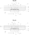
- FIG. 2a illustrates an integrated optical transceiver 100 according to a first aspect of the present invention.
- the integrated optical transceiver 100 is similar to the integrated optical transceiver 1 in many respects, and in particular all which has been said above regarding the integrated optical transceiver 1 is equally applicable to integrated optical transceiver 100, unless otherwise is stated. The same is true regarding the below described integrated optical transceivers 200 and 300.
- the integrated optical transceiver 100 shares the same reference numerals, for identical or corresponding features, with the one shown in Figure 1 , but with a "1" before each respective reference numeral. The corresponding is also true regarding Figures 2b-6 .
- the integrated optical transceiver 100 also comprises a heat sink 110, a first heat sink, in the form of a connected piece of material arranged to transport excess heat away from the integrated optical transceiver 100, which first heat sink 100 is thermally connected to both the laser driving component 170 and the photodiode driving component 140.
- the first heat sink 100 may be connected to the respective substrate 142, 172 of the laser driving component 170 and the photodiode driving component 140, as illustrated in Figure 2a on the side of each of said components 140, 170 facing away from the photodiodes 151 in the height direction H.
- the integrated optical transceiver 100 comprises an electrically insulating material 153 separating the photodiode substrate 152 from the first heat sink 100 in the height direction H.
- the insulating material 153 is air.
- the insulating material may alternatively be any dielectric material with a relative dielectric constant ⁇ ⁇ 10. Examples include the material Thermoset SC-324, marketed by the company Lord, Cary, USA.
- the electrically insulating material 153 provides an electric gap between the photodiode substrate 152 and the first heat sink 100, the effective electrical distance of which gap is at least 80 ⁇ m in the height direction H across the whole photodiode component 150, in particular providing such an electrical distance between the first heat sink 110 and the photodiode 151 anode and cathodes.
- the laser component 160 and in particular the laser diode substrate 162, is in direct thermal contact with the first heat sink 110.
- both the laser component 160, the laser driving component 170 and the photodiode driving component 140, and in particular the respective substrates 162, 172, 142 of said components, may be thermally connected to the first heat sink 100.
- Such thermal connection may be a direct physical connection, or alternatively an indirect physical connection via a thermally conductive material.
- FIG. 2b An example of the latter alternative is shown in Figure 2b , wherein a thermally conducting material 190 is arranged between, at a first side (lower side in Figure 2b ) of the thermally conducting material 190, the laser component 160, the laser driving component 170 and the photodiode driving component 140, and, at a second side of the thermally conducting material 190 (upper side in Figure 2b ), the first heat sink 110.
- the thermally conductive material 190 may also be electrically conductive.
- the thermal conductivity of the material 190 is at least 2 W/(m ⁇ K).
- the electric conductivity of the material 190 is at least 1 S/m.
- suitable materials include materials made of mixtures of nickel and dielectric materials.
- the thermally conducting material 190 is further arranged to absorb thermally induced mechanical movements between the first heat sink 110, the laser component 160, the laser driving component 170 and the photodiode driving component 140.
- the thermally conducting material 190 may have a hardness of 40-70, preferably 45-60, preferably about 50, on the Shore A scale.
- the thermally conducting material 190 is a dielectric material, with an effective electrical thickness of the thermally conducting material 190, in the height direction H, of at the most 10 ⁇ m.
- the relative dielectric constant ⁇ of the thermally conducting material 190 may be around 4. For many applications, 2.5 ⁇ of the material should be less than the electrical distance in the height direction H for the thermally conducting material 190.
- the thermally conducting material 190 may be arranged only to cover, in the longitudinal L and lateral W directions, the photodiode driving component 140, the photodiode component 150 and the laser driving component 170, as is illustrated in Figure 2b . In particular, it is not arranged to cover or thermally or directly contact the laser component 160.
- thermally conductive material 190 separating the components 140, 160, 170 from the first heat sink 110, sufficient cooling can be achieved with low crosstalk while still achieving a very robust, mechanically stable and temperature gradient resisting structure.
- the laser driving component 170 and the photodiode driving component 140 are both arranged on one common flat non-conductive substrate 120.
- a ground plane 321 which not shown in Figures 2a-2c , but is illustrated in Figure 3 , is attached to the common substrate, which ground plane 321 comprises at least one through opening 321a surrounding the photodiodes 351.
- the photodiodes 351 are connected to the photodiode driving component 340, and in particular to the photodiode driving circuitry, using conductors 351a.
- a lateral width direction W of the integrated optical transceiver is also shown, together with the above discussed longitudinal direction L.
- said at least one opening 321a in the ground plane only comprises such one or several openings 321a each having a respective resonance frequency which is at least three times higher than a fundamental frequency of a crosstalk signal resulting from the laser driving component to the photodiode component and/or photodiode driving component 340.
- each individual photodiode 31 may be surrounded by its own respective opening 321a in the ground plane 321, which openings 321a are then separated by respective bridge parts 321b, 321c of said ground plane 321.
- the openings 321a may be arranged in clusters of a few (such as between 4 and 8) openings with relatively narrow bridge parts 321b, which clusters are then separated by relatively broad bridge parts 321c. It is noted that the word "relatively” here relates to a comparison of respective widths (in the lateral direction W) of different bridge parts 321b, 321c.
- ground plane 321 configuration is particularly advantageous together with a thermal relief arrangement according to the first, second or third aspects of the present invention as described herein.
- thermal relief strategies are coupled with such ground plane 321 configurations.
- this is true in the presently described case wherein most of the crosstalk noise originate between the laser diode and the photodiode.
- ground plane 321 configuration illustrated in Figure 3 can be combined with any and all of the embodiments described herein of the present invention.
- the photodiode component 150 is arranged with a lower height, perpendicularly to the flat substrate 120 in the height direction H, than both the laser driving component 170 and the photodiode driving component 140, hence forming the above described electric gap.
- this can equally well be done by lowering the height of the photodiode component 150 and/or by raising the height of the laser diode component 160. In the latter case, the height of the photodiode driving component 140 and/or the laser diode driving component 170 may then also be raised.
- the first heat sink 110 has a non-uniform thickness, in a direction perpendicular to said substrate 120 (the height direction H).
- the said thickness is smaller in the vicinity of the photodiode component 150 than in the vicinity of the laser driving component 170 and the photodiode driving component 140, and preferably also in the vicinity of the laser component 160, hence forming the above discussed gap.
- the said thickness is smaller across, (in the longitudinal direction L) the photodiode component 150 than across the photodiode driving component 140, the photodiode component 150 and the laser driving component 170.
- Figure 2c illustrates the first heat sink 110 comprising two discreet but connected layers 110a, 110b, wherein a first one 110a of said layers extends across both the photodiode component 150, the laser driving component 170 and the photodiode driving component 140, and preferably also across the laser component 160. Furthermore, a second one 110b of said layers, facing the photodiode component 150, extends across the laser driving component 170 and the photodiode driving component 140, and preferably also across the laser component 160, but not across the photodiode component 150, hence forming said gap.
- the layers 110a, 110b may be attached to each other in any suitable conventional manner. They may also be part of the same connected and integrated material body, such as a single body of aluminium, where the interruptions of layer 110b are formed as indentations or recesses from below in said single body.
- first heat sink 110 and as the case may be the first 110a and second 110b layer, are made of a metal material, such as a highly doped semiconductor material or a metal or metal alloy, such as aluminium.
- Figure 4 illustrates an integrated optical transceiver 200 according to a second aspect of the present invention.
- transceivers 1 and 100 are applicable to relevant parts.
- the integrated optical transceiver 200 like the transceiver 100, comprises a laser component 260, in turn comprising an array of VCSEL diodes 261 formed on a laser diode substrate 262; a laser driving component 270, in turn comprising laser diode driving circuitry 271 formed on a laser driving circuitry substrate 272; a photodiode component 250, in turn comprising an array of photodiodes 251 formed on a photodiode substrate 252; and a photodiode driving component 240, in turn comprising photodiode driving circuitry 241 formed on a photodiode driving circuitry substrate 242. Materials for these components may be same as for transceiver 100, discussed above.
- the integrated optical transceiver 200 further comprises a first heat sink 210, arranged to transport excess heat away from the integrated optical transceiver 200.
- the first heat sink 210 of transceiver 200 comprises, such as is constituted by, a connected piece of semiconductor material, which is connected to both the photodiode component 250, the laser driving component 270 and the photodiode driving component 240, and preferably also to the laser component 260.
- That the first heat sink 210 is "connected" to these components 240, 250, 260, 270 means that it is thermally connected to the components 240, 250, 260, 270 in question, in a way which may be similar to the above-discussed thermal connection of the first heat sink 110 to the components 140, 150, 160, 170.
- the thermal connection in question may be a direct physical connection, or alternatively an indirect physical connection via a thermally conductive material.
- the semiconductor material of the first heat sink 210 has an electrical conductivity of between 0.1 and 15 Ohms ⁇ cm, preferably 1 and 15 Ohms ⁇ cm, preferably around 10 Ohms ⁇ cm. Specifically, if the semiconductor material of the first heat sink 210 is too little doped, it becomes dielectric, resulting in resonance problems. If it is too highly doped, it becomes a metal, resulting in increased crosstalk.
- Suitable semiconductor materials include doped Si and SiC, or corresponding semiconductor materials, with high thermal conductivity, such as at least 100 W/(m ⁇ K).
- the semiconductor material may be doped Si with thermal conductivity 370 W/(m ⁇ K) or doped SiC with thermal conductivity of at least 150 W/(m ⁇ K).
- the mentioned electrical conductivity of about 10 Ohm ⁇ cm, provides significant loss and hence mitigates crosstalk noise.
- Suitable materials are optimized for high mechanical stability and high thermal conductivity, while observing said limits for electric conductivity.
- the laser diode component 260 is in direct contact, such as in direct thermal contact, with the first heat sink 210.
- the semiconductor material of the first heat sink 210 may have a thickness of at least 200 ⁇ m, such as at least 400 ⁇ m, and may also have a thickness of at the most 1000 ⁇ m. Preferably, the thickness is about 500 ⁇ m.
- the integrated optical transceiver 200 may comprise a second heat sink 211, arranged at a side of the first heat sink 210 facing away, in the height direction H, from the common planar substrate 220.
- the first 210 and second 211 heat sinks may be separated by a second layer of thermal gap pad material 290b.
- the second heat sink 211 may be manufactured from similar materials as the first heat sink 110 of the transceiver 100, such as aluminium.
- the transceiver 200 may also comprise a first thermally conducting material 290a, arranged between, at a first side of the first thermally conducting material 290a, the laser component 260, the laser driving component 270 and the photodiode driving component 240, and preferably also the photodiode component 250, and, at a second side of the first thermally conducting material 290a, the first heat sink 210.
- This first thermally conducting material 290a may, similarly, be arranged to absorb thermally induced mechanical movements between the first heat sink 210, the laser component 260, the laser driving component 270 and the photodiode driving component 240.
- the first thermally conductive material may be electrically conductive.
- the first thermally conducting material 290a is a dielectric material, the effective electrical thickness of which may be at least 50 ⁇ m, preferably at least 80 ⁇ m.
- the first thermally conducting material 290a has a hardness of 40-70, preferably 45-60, preferably about 50, on the Shore A scale, similarly to the thermally conductive material 190.
- the first thermally conducting material 290a may be arranged in direct contact with the laser component 260, the laser driving component 270, the photodiode component 250 and the photodiode driving component 240.
- the relative dielectric constant ⁇ of the thermally conducting material 290a may be around 4. For many applications, 2.5 ⁇ of the material should be less than the electrical distance in the height direction H for the thermally conducting material 290. The same applies also to the thermally conducting material 390a (see below).
- the second thermally conducting material 290b layer may be of similar material constitution as the first thermally conducting material 290a.
- a similar thermally conducting material 290c may also be used to fill the void between the components 240, 250, 260, 270.
- Such a constitution according to this second aspect of the present invention provides similar advantages as that of the first aspect of the present invention.
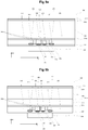
- Figure 5a illustrates an integrated optical transceiver 300 according to a third aspect of the present invention, comprising a laser component 360, in turn comprising an array of VCSEL diodes 361 formed on a laser diode substrate 362; a laser driving component 370, in turn comprising laser diode driving circuitry 371 formed on a laser driving circuitry substrate 372; a photodiode component 350, in turn comprising an array of photodiodes 351 formed on a photodiode substrate 352; and a photodiode driving component 340, in turn comprising photodiode driving circuitry 341 formed on a photodiode driving circuitry substrate 342.
- the integrated optical transceiver 300 further comprises a first heat sink 310, in turn comprising, preferably consisting of, a connected piece of magnetic absorbing material arranged to transport excess heat away from the integrated optical transceiver 300.
- the first heat sink 310 is connected to both the photodiode component 350, the laser driving component 370 and the photodiode driving component 340, and preferably also to the laser component 360.
- "connected to” has the same interpretation as given above for the first heat sinks 110, 210.
- the magnetic absorbing material of the first heat sink 310 is either magnetic microwave absorber material or lossy ferrite.
- the laser diode substrate 362 may be in direct contact with the first heat sink 310.
- the magnetic absorbing material 310 may have a thickness of at least 1000 ⁇ m, preferably at least 1500 ⁇ m. Preferably, the magnetic absorbing material 310 has a thickness of at the most 3000 ⁇ m. The magnetic absorbing material 310 may have a thickness of about 2000 ⁇ m.
- the magnetic absorbing material 310 may have a relative magnetic permeability ⁇ of at least 10 and a magnetic loss tangent tan ⁇ e of at least 0.1, such as about 0.5.
- the integrated optical transceiver 300 may further comprise a second heat sink 311, arranged at the side of the first heat sink 310, in the height direction H, facing away from the substrate 320, which first 310 and second 311 heat sinks are separated by a second thermal gap pad material 390b.
- the second heat sink 311 may be manufactured from similar materials as the first heat sink 110 of the transceiver 100, such as aluminium.
- the integrated optical transceiver 300 furthermore comprises a first thermally conducting material 390a, arranged between, at a first side of the first thermally conducting material 390a, the laser component 360, the laser driving component 370 and the photodiode driving component 340, and preferably also the photodiode component 350, and, at a second side of the first thermally conducting material 390a, the first heat sink 310, which thermally conducting material is arranged to absorb thermally induced mechanical movements between the first heat sink 310, the laser component 360, the laser driving component 370 and the photodiode driving component 340.
- the first thermally conducting material 390a may be similar to the thermally conducting material 290a of transceiver 200. As such, it may be electrically conductive or dielectric with an effective electrical thickness of which is at least 50 ⁇ m, preferably at least 80 ⁇ m. It also may have a hardness of 40-70, preferably 45-60, preferably about 50, on the Shore A scale.
- the first thermally conducting material 390a may also be arranged in direct contact with the laser component 260, the laser driving component 270, the photodiode component 250 and the photodiode driving component 240.
- the second thermally conducting material 390b may be arranged, in the height direction H, between the first heat sink 310 and the second heat sink 311, in a way similar to the second thermally conducting material 290b. Also, a similar thermally conducting material 390c may be arranged to fill the void between the components 340, 350, 360, 370.
- Figure 5b illustrates an alternative embodiment of the third aspect of the present invention, in which the first heat sink 310 further comprises a lower (in the height direction H) layer 310a of the above discussed magnetic absorber material, as well as an upper layer 310b of metal or dielectric material arranged at a side of the magnetic absorbing material facing away from the substrate 320 in the height direction H.
- the first heat sink 310 consists of a sandwich material comprising the medium thermally conductive magnetic absorber material 310a and high thermal conductivity (metal or dielectric) material 310b.
- the high thermal conductivity material 310b may for instance be aluminium or CVD diamond.
- the first thermal gap material 390a may be substituted partially or fully by the magnetic absorber material 310a. This is possible in both embodiments shown in Figures 5a and 5b .
- This third aspect of the present invention also provides similar advantages as the first and second aspects described above.
- a voltage electric signal applied by the laser diode driving circuitry 171, 271, 371 to the laser component 160, 260, 360 has a frequency of at least 100 MHz.
- the present invention further relates to an integrated optical circuit 600 comprising an optical transceiver 100, 200, 300 according to the first, second or third aspects of the invention.
- a circuit 600 is illustrated in Figure 6 .
- FIGS 7a, 7b and 7c are respective charts depicting crosstalk magnitudes for detailed simulations run in relation to a respective model of an integrated optical circuits according to the first, second and third aspect of the present invention.
- Each chart shows principal Tx-Rx coupling s-parameters (electric connection across various paths between transmitter and receiver part, in dB (Y axis) to frequency in GHz (X axis)) in 16 channel module.
- Inner and outer contours correspond to the case with and without crosstalk, respectively. As is clear from each of these charts, inner and outer contours coincide, corresponding to no observed crosstalk.
- Figures 8a and 8b illustrate the corresponding charts for two different configurations not according to the invention; in Figure 8a , both the laser component and the photodiode component are directly attached to one and the same metal heat sink, while in Figure 8b , the same configuration is used but with a thin thermoset gap material between the components and the heat sink.
- inner eye diagram contours are smaller than outer contours, corresponding to significant electric crosstalk.
- an integrated optical transceiver comprising
- the laser diode substrate is in direct contact with the first heat sink.
- the semiconductor material has a thickness of at least 200 ⁇ m.
- the semiconductor material is doped Si or SiC, or corresponding semiconductor material having a thermal conductivity of at least 100 W/(m ⁇ K).
- the laser driving component and the photodiode driving component are arranged on one common flat non-conductive substrate.
- a ground plane is attached to the common substrate, which ground plane comprises at least one opening surrounding the said photodiodes.
- said at least one opening only comprises openings having a respective resonance frequency which is at least three times higher than a fundamental frequency of a crosstalk signal resulting from the laser driving component to the photodiode driving component.
- each individual photodiode is surrounded by its own respective opening in the ground plane, which openings are separated by bridge parts of said ground plane.
- the integrated optical transceiver further comprises a second heat sink, arranged at a side of the first heat sink facing away from the substrate, which first and second heat sinks are separated by a thermal gap pad material.
- the photodiodes are Positive Intrinsic Negative (PIN) photodiodes.
- a thermally conducting material is arranged between, at a first side of the thermally conducting material, the laser component, the laser driving component and the photodiode driving component, and, at a second side of the thermally conducting material, the first heat sink, which thermally conducting material is arranged to absorb thermally induced mechanical movements between the first heat sink, the laser component, the laser driving component and the photodiode driving component.
- the thermally conducting material is electrically conductive.
- the thermally conducting material is dielectric, and the effective electrical thickness of which is at least 50 ⁇ m, preferably at least 80 ⁇ m.
- the thermally conducting material has a hardness of 40-70, preferably 45-60, preferably about 50, on the Shore A scale.
- the thermally conducting material is arranged in direct contact with the laser component, the laser driving component, the photodiode component and the photodiode driving component.
- an electrical signal applied by the laser diode driving circuitry to the laser component has a frequency of at least 100 MHz.
- an integrated optical transceiver comprising
- the laser diode substrate is in direct contact with the first heat sink.
- the magnetic absorbing material has a thickness of at least 1000 ⁇ m.
- the magnetic absorbing material has a relative magnetic permeability ⁇ of at least 10 and a magnetic loss tangent tan ⁇ e of at least 0.1.
- the laser driving component and the photodiode driving component are arranged on one common flat non-conductive substrate.
- a ground plane is attached to the common substrate, which ground plane comprises at least one opening surrounding the said photodiodes.
- said at least one opening only comprises openings having a respective resonance frequency which is at least three times higher than a fundamental frequency of a crosstalk signal resulting from the laser driving component to the photodiode driving component.
- each individual photodiode is surrounded by its own respective opening in the ground plane, which openings are separated by bridge parts of said ground plane.
- the integrated optical transceiver further comprises a second heat sink, arranged at the side of the first heat sink facing away from the substrate, which first and second heat sinks are separated by a thermal gap pad material.
- the first heat sink further comprises a layer of metal or dielectric material arranged at a side of the magnetic absorbing material facing away from the substrate.
- the photodiodes are Positive Intrinsic Negative (PIN) photodiodes.
- a thermally conducting material is arranged between, at a first side of the thermally conducting material, the laser component, the laser driving component and the photodiode driving component, and, at a second side of the thermally conducting material, the first heat sink, which thermally conducting material is arranged to absorb thermally induced mechanical movements between the first heat sink, the laser component, the laser driving component and the photodiode driving component.
- the thermally conducting material is electrically conductive.
- the thermally conducting material is dielectric, and wherein the effective electrical thickness of which is at least 50 ⁇ m, preferably at least 80 ⁇ m.
- the thermally conducting material has a hardness of 40-70, preferably 45-60, preferably about 50, on the Shore A scale.
- the thermally conducting material is arranged in direct contact with the laser component, the laser driving component, the photodiode component and the photodiode driving component.
- a voltage electric signal applied by the laser diode driving circuitry to the laser component has a frequency of at least 100 MHz.
- the invention also relates to an integrated optical circuit comprising an optical transceiver of any one of the above described types.
- the integrated optical transceivers described herein may comprise additional layers and features, apart from the ones described.
- the corresponding is true regarding the integrated optical circuit according to the invention.
- the above described first and second heat sinks may transport the heat away using for instance forced air convection, such as by using a conventional fan.
Landscapes
- Physics & Mathematics (AREA)
- Optics & Photonics (AREA)
- General Physics & Mathematics (AREA)
- Electromagnetism (AREA)
- Condensed Matter Physics & Semiconductors (AREA)
- Engineering & Computer Science (AREA)
- Computer Networks & Wireless Communication (AREA)
- Signal Processing (AREA)
- Semiconductor Lasers (AREA)
Abstract
Description
- The present invention relates to an integrated optical transceiver, and in particular to a short range fiber optical transceiver. Typically, such an integrated optical transceiver is arranged for optical communication across distances of less than 1 km, across several, such as at least 12, preferably at least 16, communication channels and at bit rates per channel of at least 25 Gb/s.
- In particular, the present invention relates to such integrated optical transceivers using an array of VCSEL (Vertical-Cavity Surface-Emitting Laser) diodes for light emission.
- Such integrated optical transceivers typically also feature an array of photodiodes, arranged next to the VCSEL diodes across a substrate. Hence, light is both emitted and received in the same direction, perpendicularly to the substrate main plane.
- A problem for such integrated optical transceivers is cooling of the transceiver. In order to cool the components adequately, it has been proposed to arrange a metal heat sink across the back side of the components of the integrated optical transceiver, via which excess heat can be transported away. However, such metal heat sink has a tendency to produce crosstalk between VCSEL diode driving circuitry and an amplifier component comprised in a photodiode driving circuitry. Typically, the current to the VCSEL is many times larger than the current from the said amplifier, why such crosstalk noise limits the performance of the integrated optical transceiver.
- At the same time, temperature differences produce mechanical stress in such an integrated optical transceiver, which may lead to material deterioration or even breakage.
- Hence, an integrated optical transceiver would be desirable that is both efficiently cooled, displays minimal crosstalk noise and which is mechanically stable.
- The present invention solves the above described problems.
- Hence, the invention relates to, in a first aspect, an integrated optical transceiver, comprising a laser component, in turn comprising an array of VCSEL (Vertical-Cavity Surface-Emitting Laser) diodes formed on a laser diode substrate; a laser driving component, in turn comprising laser diode driving circuitry formed on a laser driving circuitry substrate; a photodiode component, in turn comprising an array of photodiodes formed on a photodiode substrate; and a photodiode driving component, in turn comprising photodiode driving circuitry formed on a photodiode driving circuitry substrate; which optical transceiver further comprises a first heat sink in the form of a connected piece of material arranged to transport excess heat away from the integrated optical transceiver, which first heat sink is connected to both the laser driving component and the photodiode driving component; and an electrically insulating material separating the photodiode substrate from the first heat sink, which electrically insulating material is either air or a dielectric material with a relative dielectric constant ε < 10, wherein the electrically insulating material provides a gap between the photodiode substrate and the first heat sink, the effective electrical distance of which gap is at least 80 µm.
- In such an integrated optical transceiver, the laser diode substrate may be in direct contact with the first heat sink.
- In such an integrated optical transceiver, the laser driving component and the photodiode driving component may arranged on one common flat non-conductive substrate.
- In such an integrated optical transceiver, a ground plane may be attached to the common substrate, which ground plane also may comprise at least one opening surrounding the said photodiodes.
- In such an integrated optical transceiver, said at least one opening may only comprise openings having a respective resonance frequency which is at least three times higher than a fundamental frequency of a crosstalk signal resulting from the laser driving component to the photodiode driving component.
- In such an integrated optical transceiver, each individual photodiode may be surrounded by its own respective opening in the ground plane, which openings in turn may be separated by bridge parts of said ground plane.
- In such an integrated optical transceiver, the photodiode component may be arranged with a lower height, perpendicularly to the flat substrate, than both the laser driving component and the photodiode driving component, hence forming the gap.
- In such an integrated optical transceiver, the first heat sink may have a non-uniform thickness, in a direction perpendicular to said substrate, which thickness may be smaller in the vicinity of the photodiode component than in the vicinity of the laser driving component and the photodiode driving component, hence forming the gap.
- In such an integrated optical transceiver, the first heat sink may comprise two discreet but connected layers, wherein a first one of said layers may extend across both the photodiode component, the laser driving component and the photodiode driving component, and wherein a second one of said layers, facing the photodiode component, may extend across the laser driving component and the photodiode driving component but not across the photodiode component.
- In such an integrated optical transceiver, the photodiodes may be Positive Intrinsic Negative (PIN) photodiodes.
- In such an integrated optical transceiver, a thermally conducting material may be arranged between, at a first side of the thermally conducting material, the laser component, the laser driving component and the photodiode driving component, and, at a second side of the thermally conducting material, the first heat sink, which thermally conducting material in turn may be arranged to absorb thermally induced mechanical movements between the first heat sink, the laser component, the laser driving component and the photodiode driving component.
- In such an integrated optical transceiver, the thermally conducting material may be electrically conductive.
- In such an integrated optical transceiver, the thermally conducting material may be a dielectric material, and the effective electrical thickness of the thermally conducting material may be at the most 10 µm.
- In such an integrated optical transceiver, the thermally conducting material may have a hardness of 40-70, preferably 45-60, preferably about 50, on the Shore A scale.
- In such an integrated optical transceiver, the first heat sink may be made of a metal material.
- In such an integrated optical transceiver, an electrical signal being applied by the laser diode driving circuitry to the laser component may have a frequency of at least 100 MHz.
- In a second aspect, the present invention relates to an integrated optical transceiver, comprising a laser component, in turn comprising an array of VCSEL (Vertical-Cavity Surface-Emitting Laser) diodes formed on a laser diode substrate; a laser driving component, in turn comprising laser diode driving circuitry formed on a laser driving circuitry substrate; a photodiode component, in turn comprising an array of photodiodes formed on a photodiode substrate; and a photodiode driving component, in turn comprising photodiode driving circuitry formed on a photodiode driving circuitry substrate; which optical transceiver further comprises a first heat sink in the form of a connected piece of semiconductor material arranged to transport excess heat away from the integrated optical transceiver, which first heat sink is connected to both the photodiode component, the laser driving component and the photodiode driving component, which semiconductor material has an electrical conductivity of between 0.1 and 15 Ohms·cm, preferably 1 and 15 Ohms·cm, preferably around 10 Ohms·cm.
- In such an integrated optical transceiver, the laser diode substrate may be in direct contact with the first heat sink.
- In such an integrated optical transceiver, the semiconductor material may have a thickness of at least 200 µm.
- In such an integrated optical transceiver, the semiconductor material may be doped Si or SiC, or corresponding semiconductor material having a thermal conductivity of at least 100 W/(m·K).
- In such an integrated optical transceiver, the laser driving component and the photodiode driving component may be arranged on one common flat non-conductive substrate.
- In such an integrated optical transceiver, a ground plane may be attached to the common substrate, which ground plane comprises at least one opening surrounding the said photodiodes.
- In such an integrated optical transceiver, said at least one opening only may comprise openings having a respective resonance frequency which is at least three times higher than a fundamental frequency of a crosstalk signal resulting from the laser driving component to the photodiode driving component.
- In such an integrated optical transceiver, each individual photodiode may be surrounded by its own respective opening in the ground plane, which openings in turn may be separated by bridge parts of said ground plane.
- In such an integrated optical transceiver, the integrated optical transceiver may further comprise a second heat sink, arranged at a side of the first heat sink facing away from the substrate, which first and second heat sinks in turn may be separated by a thermal gap pad material.
- In such an integrated optical transceiver, the photodiodes may be Positive Intrinsic Negative (PIN) photodiodes.
- In such an integrated optical transceiver, a thermally conducting material may be arranged between, at a first side of the thermally conducting material, the laser component, the laser driving component and the photodiode driving component, and, at a second side of the thermally conducting material, the first heat sink, which thermally conducting material in turn may be arranged to absorb thermally induced mechanical movements between the first heat sink, the laser component, the laser driving component and the photodiode driving component.
- In such an integrated optical transceiver, the thermally conducting material may be electrically conductive.
- In such an integrated optical transceiver, the thermally conducting material may be dielectric, and wherein the effective electrical thickness of which may be at least 50 µm, preferably at least 80 µm.
- In such an integrated optical transceiver, the thermally conducting material may have a hardness of 40-70, preferably 45-60, preferably about 50, on the Shore A scale.
- In such an integrated optical transceiver, the thermally conducting material may be arranged in direct contact with the laser component, the laser driving component, the photodiode component and the photodiode driving component.
- In such an integrated optical transceiver, an electrical signal which is applied by the laser diode driving circuitry to the laser component, may have a frequency of at least 100 MHz.
- In a third aspect, the present invention relates to an integrated optical transceiver, comprising a laser component, in turn comprising an array of VCSEL (Vertical-Cavity Surface-Emitting Laser) diodes formed on a laser diode substrate; a laser driving component, in turn comprising laser diode driving circuitry formed on a laser driving circuitry substrate; a photodiode component, in turn comprising an array of photodiodes formed on a photodiode substrate; and a photodiode driving component, in turn comprising photodiode driving circuitry formed on a photodiode driving circuitry substrate; which optical transceiver further comprises a first heat sink comprising a connected piece of magnetic absorbing material arranged to transport excess heat away from the integrated optical transceiver, which first heat sink is connected to both the photodiode component, the laser driving component and the photodiode driving component, which magnetic absorbing material is either magnetic microwave absorber material or lossy ferrite.
- In such an integrated optical transceiver, the laser diode substrate may be in direct contact with the first heat sink.
- In such an integrated optical transceiver, the magnetic absorbing material may have a thickness of at least 1000 µm.
- In such an integrated optical transceiver, the magnetic absorbing material may have a relative magnetic permeability µ of at least 10 and a magnetic loss tangent tan δ of at least 0.1.
- In such an integrated optical transceiver, the laser driving component and the photodiode driving component may be arranged on one common flat non-conductive substrate.
- In such an integrated optical transceiver, a ground plane may be attached to the common substrate, which ground plane in turn may comprise at least one opening surrounding the said photodiodes.
- In such an integrated optical transceiver, said at least one opening may only comprise openings in turn having a respective resonance frequency which is at least three times higher than a fundamental frequency of a crosstalk signal resulting from the laser driving component to the photodiode driving component.
- In such an integrated optical transceiver, each individual photodiode may be surrounded by its own respective opening in the ground plane, which openings in turn may be separated by bridge parts of said ground plane.
- In such an integrated optical transceiver, the integrated optical transceiver may further comprise a second heat sink, arranged at the side of the first heat sink facing away from the substrate, which first and second heat sinks in turn may be separated by a thermal gap pad material.
- In such an integrated optical transceiver, the first heat sink may further comprise a layer of metal or dielectric material arranged at a side of the magnetic absorbing material facing away from the substrate.
- In such an integrated optical transceiver, the photodiodes may be Positive Intrinsic Negative (PIN) photodiodes.
- In such an integrated optical transceiver, a thermally conducting material may be arranged between, at a first side of the thermally conducting material, the laser component, the laser driving component and the photodiode driving component, and, at a second side of the thermally conducting material, the first heat sink, which thermally conducting material in turn may be arranged to absorb thermally induced mechanical movements between the first heat sink, the laser component, the laser driving component and the photodiode driving component.
- In such an integrated optical transceiver, the thermally conducting material may be electrically conductive.
- In such an integrated optical transceiver, the thermally conducting material may be dielectric, the effective electrical thickness of which may be at least 50 µm, preferably at least 80 µm.
- In such an integrated optical transceiver, the thermally conducting material may have a hardness of 40-70, preferably 45-60, preferably about 50, on the Shore A scale.
- In such an integrated optical transceiver, the thermally conducting material may be arranged in direct contact with the laser component, the laser driving component, the photodiode component and the photodiode driving component.
- In such an integrated optical transceiver, a voltage electric signal applied by the laser diode driving circuitry to the laser component, may have a frequency of at least 100 MHz.
- Finally, the invention also relates to an integrated optical circuit comprising an optical transceiver according to any one of the said first, second or third aspects.
- In the following, the invention will be described in detail, with reference to exemplifying embodiments of the invention and to the enclosed drawings, wherein:
-
Figure 1 illustrates an integrated optical transceiver not according to the present invention; -
Figures 2a-2c illustrate an integrated optical transceiver according to a first aspect of the present invention; -
Figure 3 is a detail view of an integrated optical transceiver according to the present invention; -
Figure 4 illustrates an integrated optical transceiver according to a second aspect of the present invention; -
Figures 5a and 5b illustrate an integrated optical transceiver according to a third aspect of the present invention; -
Figure 6 illustrates an integrated optical circuit according to the present invention; -
Figures 7a-7c illustrate simulated performance parameters for an integrated optical transceiver according to the first, second and third aspects, respectively; and -
Figures 8a and 8b illustrate simulated performance parameters for a respective integrated optical transceiver not according to the present invention. - The Figures share reference numerals for same or corresponding parts, except for the first digit in each three digit reference numeral, that may differ between different aspects of the present invention as described herein. The
Figures 1-6 are all schematic and simplified, and not drawn to scale. - Hence,
Figure 1 illustrates an integratedoptical transceiver 1 which is not according to the present invention, but whichtransceiver 1 is associated with a length direction L and a height direction H. A lateral direction H (seeFigure 3 ) is oriented perpendicularly to the paper.Figure 1 does not show details that are conventional as such. - That the
optical transceiver 1 is "integrated" means that it is made from one single material body, in the sense that it cannot be disassembled, and not in the sense that the material body is homogenous in its constitution. It may be produced using methods such as epitaxial growth and etching. The integratedoptical transceiver 1 may exist and be used as an optical transceiver on an integrated circuit also comprising additional components. Typical fields of use include circuitry for short-range high-frequency optical communication, such as within a data centre. - The integrated
optical transceiver 1 comprises aflat substrate layer 20, which comprises a ground plane; alaser component 60, in turn comprising an array of VCSEL (Vertical-Cavity Surface-Emitting Laser)diodes 61 formed on thelaser diode substrate 62; alaser driving component 70, in turn comprising laserdiode driving circuitry 71 formed on a laser drivingcircuitry substrate 72; aphotodiode component 50, in turn comprising an array ofphotodiodes 51 formed on aphotodiode substrate 52; and aphotodiode driving component 40, in turn comprisingphotodiode driving circuitry 41 formed on a photodiodedriving circuitry substrate 42. Thephotodiode driving circuitry 41 may comprise a TIA (Trans Impedance Amplifier, not shown). - The
photodiodes 51 may be of any suitable type, such as Positive Intrinsic Negative (PIN) photodiodes. - The integrated
optical transceiver 1 further comprises aglass material 30 covering thephotodiodes 51 and thelaser diodes 71. Theglass material 30 may for instance be a borosilicate glass. Furthermore, the integratedoptical transceiver 1 comprises an integratedcircuit underfill material 80, between thesubstrate 20 and each of thediodes circuitry underfill material 80 may for instance be an epoxy resin. - The integrated
optical transceiver 1 further comprisesheat sink 10, which is connected by direct physical attachment to thesubstrates components - The photodiode
driving circuitry substrate 42, and also the laser diode drivingcircuitry substrate 71, may be made from a semiconductor material such as Si, for instance having a dielectric constant ε of 11.9 and electric conductivity of 6.7 S/m. Thephotodiode substrate 52 may be made from a dielectric material having a high dielectric constant ε, such as having a dielectric constant ε = 13.1, and with an electric conductivity of 1.8E-6 S/m. Thelaser diode substrate 62 may be made from a highly doped material (essentially being a metal material), such as having an electric conductivity of 5.0E4 S/m. - Thus, during operation, light enters the
transceiver 1 in the height direction H from below inFigure 1 , through theglass material 30, is detected by thephotodiodes 51 and corresponding electrical signals are processed by thephotodiode driving circuitry 41, which in turn delivers electric signals corresponding to information carried by the received light to an electric port for further communication and/or data processing. - Correspondingly, the
laser driving circuitry 71 receives electric signals from a suitable electric port, and feeds processed electric signals to theVCSEL laser diodes 61 which emits corresponding laser light. The emitted laser light exits the component through theglass 30 material. - The
heat sink 10, which may for instance be a homogenous body of metal material, is arranged to remove excess heat from the component, and in particular from thelaser diodes 51 and the drivingcircuitry heat sink 10 also leads to significant crosstalk between thevarious components - In particular, the present inventors have discovered that such crosstalk arises from the laser
diode driving circuitry 71 to thephotodiodes 51, to such a level that signal detection becomes associated with much noise and is significantly affected in terms of accuracy and resulting data speeds. -
Figure 2a illustrates an integratedoptical transceiver 100 according to a first aspect of the present invention. The integratedoptical transceiver 100 is similar to the integratedoptical transceiver 1 in many respects, and in particular all which has been said above regarding the integratedoptical transceiver 1 is equally applicable to integratedoptical transceiver 100, unless otherwise is stated. The same is true regarding the below described integratedoptical transceivers - The integrated
optical transceiver 100 shares the same reference numerals, for identical or corresponding features, with the one shown inFigure 1 , but with a "1" before each respective reference numeral. The corresponding is also true regardingFigures 2b-6 . - As illustrated in
Figure 2a , the integratedoptical transceiver 100 also comprises aheat sink 110, a first heat sink, in the form of a connected piece of material arranged to transport excess heat away from the integratedoptical transceiver 100, whichfirst heat sink 100 is thermally connected to both thelaser driving component 170 and thephotodiode driving component 140. In particular, thefirst heat sink 100 may be connected to therespective substrate laser driving component 170 and thephotodiode driving component 140, as illustrated inFigure 2a on the side of each of saidcomponents photodiodes 151 in the height direction H. - Furthermore, the integrated
optical transceiver 100 comprises an electrically insulatingmaterial 153 separating thephotodiode substrate 152 from thefirst heat sink 100 in the height direction H. InFigure 2a , the insulatingmaterial 153 is air. However, the insulating material may alternatively be any dielectric material with a relative dielectric constant ε < 10. Examples include the material Thermoset SC-324, marketed by the company Lord, Cary, USA. - According to this first aspect of the present invention, the electrically insulating
material 153 provides an electric gap between thephotodiode substrate 152 and thefirst heat sink 100, the effective electrical distance of which gap is at least 80 µm in the height direction H across thewhole photodiode component 150, in particular providing such an electrical distance between thefirst heat sink 110 and thephotodiode 151 anode and cathodes. - It has turned out that such a structure is capable of providing adequate cooling of the integrated
optical transceiver 100, while at the same time limiting crosstalk noise to acceptable levels in many practical applications. In particular, crosstalk between thelaser diodes 161 and thephotodiodes 151 is limited. There are also other crosstalk paths producing noise when operating thetransceiver 100, such as within and across thephotodiode driving circuitry 141. However, the present inventors have discovered that the noise produced due to crosstalk between thelaser diodes 161 and thephotodiodes 151 is so dominating in most practical applications that limiting this noise source in the present way provides substantially improved operation noise characteristics. - According to an exemplifying embodiment, which is also shown in
Figure 2a , thelaser component 160, and in particular thelaser diode substrate 162, is in direct thermal contact with thefirst heat sink 110. - Hence, both the
laser component 160, thelaser driving component 170 and thephotodiode driving component 140, and in particular therespective substrates first heat sink 100. Such thermal connection may be a direct physical connection, or alternatively an indirect physical connection via a thermally conductive material. - An example of the latter alternative is shown in
Figure 2b , wherein a thermally conductingmaterial 190 is arranged between, at a first side (lower side inFigure 2b ) of the thermally conductingmaterial 190, thelaser component 160, thelaser driving component 170 and thephotodiode driving component 140, and, at a second side of the thermally conducting material 190 (upper side inFigure 2b ), thefirst heat sink 110. - The thermally
conductive material 190 may also be electrically conductive. Preferably, the thermal conductivity of thematerial 190 is at least 2 W/(m·K). Furthermore, it is preferred that the electric conductivity of thematerial 190 is at least 1 S/m. Examples of suitable materials include materials made of mixtures of nickel and dielectric materials. - In the configuration illustrated in
Figure 2b , the thermally conductingmaterial 190 is further arranged to absorb thermally induced mechanical movements between thefirst heat sink 110, thelaser component 160, thelaser driving component 170 and thephotodiode driving component 140. - To achieve this, the thermally conducting
material 190 may have a hardness of 40-70, preferably 45-60, preferably about 50, on the Shore A scale. - In a particularly preferred example, the thermally conducting
material 190 is a dielectric material, with an effective electrical thickness of the thermally conductingmaterial 190, in the height direction H, of at the most 10 µm. The relative dielectric constant ε of the thermally conductingmaterial 190 may be around 4. For many applications, 2.5ε of the material should be less than the electrical distance in the height direction H for the thermally conductingmaterial 190. - The thermally conducting
material 190 may be arranged only to cover, in the longitudinal L and lateral W directions, thephotodiode driving component 140, thephotodiode component 150 and thelaser driving component 170, as is illustrated inFigure 2b . In particular, it is not arranged to cover or thermally or directly contact thelaser component 160. - The use of such a thermally
conductive material 190 separating thecomponents first heat sink 110, sufficient cooling can be achieved with low crosstalk while still achieving a very robust, mechanically stable and temperature gradient resisting structure. - As illustrated in
Figures 2a-2c , thelaser driving component 170 and thephotodiode driving component 140 are both arranged on one common flatnon-conductive substrate 120. In this case, aground plane 321, which not shown inFigures 2a-2c , but is illustrated inFigure 3 , is attached to the common substrate, whichground plane 321 comprises at least one throughopening 321a surrounding thephotodiodes 351. Thephotodiodes 351 are connected to thephotodiode driving component 340, and in particular to the photodiode driving circuitry, usingconductors 351a. - In
Figure 3 , a lateral width direction W of the integrated optical transceiver is also shown, together with the above discussed longitudinal direction L. - According to one embodiment, said at least one
opening 321a in the ground plane only comprises such one orseveral openings 321a each having a respective resonance frequency which is at least three times higher than a fundamental frequency of a crosstalk signal resulting from the laser driving component to the photodiode component and/orphotodiode driving component 340. - In particular, and as illustrated in
Figure 3 , each individual photodiode 31 may be surrounded by its ownrespective opening 321a in theground plane 321, whichopenings 321a are then separated byrespective bridge parts ground plane 321. Theopenings 321a may be arranged in clusters of a few (such as between 4 and 8) openings with relativelynarrow bridge parts 321b, which clusters are then separated by relativelybroad bridge parts 321c. It is noted that the word "relatively" here relates to a comparison of respective widths (in the lateral direction W) ofdifferent bridge parts - A
similar ground plane 321 arrangement, with individual throughopenings 321a in which eachphotodiode 351 is accommodated, is described inEP 2775806 B1 , to which reference is made regarding further details. - The present inventors have discovered that the use of
such ground plane 321 configuration is particularly advantageous together with a thermal relief arrangement according to the first, second or third aspects of the present invention as described herein. Hence, particularly good noise behaviours have been detected when such thermal relief strategies are coupled withsuch ground plane 321 configurations. In particular, this is true in the presently described case wherein most of the crosstalk noise originate between the laser diode and the photodiode. - Hence, it is understood that the
ground plane 321 configuration illustrated inFigure 3 can be combined with any and all of the embodiments described herein of the present invention. - Now returning to
Figure 2a , it is noted that thephotodiode component 150 is arranged with a lower height, perpendicularly to theflat substrate 120 in the height direction H, than both thelaser driving component 170 and thephotodiode driving component 140, hence forming the above described electric gap. Starting off from a conventional integrated optical transceiver and looking to modify its configuration so as to implement the present invention, it is realized that this can equally well be done by lowering the height of thephotodiode component 150 and/or by raising the height of thelaser diode component 160. In the latter case, the height of thephotodiode driving component 140 and/or the laserdiode driving component 170 may then also be raised. - Turning to
Figure 2c , an alternative or supplementary embodiment is illustrated, in which thefirst heat sink 110 has a non-uniform thickness, in a direction perpendicular to said substrate 120 (the height direction H). The said thickness is smaller in the vicinity of thephotodiode component 150 than in the vicinity of thelaser driving component 170 and thephotodiode driving component 140, and preferably also in the vicinity of thelaser component 160, hence forming the above discussed gap. In other words, the said thickness is smaller across, (in the longitudinal direction L) thephotodiode component 150 than across thephotodiode driving component 140, thephotodiode component 150 and thelaser driving component 170. - In particular,
Figure 2c illustrates thefirst heat sink 110 comprising two discreet butconnected layers 110a, 110b, wherein a first one 110a of said layers extends across both thephotodiode component 150, thelaser driving component 170 and thephotodiode driving component 140, and preferably also across thelaser component 160. Furthermore, a second one 110b of said layers, facing thephotodiode component 150, extends across thelaser driving component 170 and thephotodiode driving component 140, and preferably also across thelaser component 160, but not across thephotodiode component 150, hence forming said gap. This provides a construction which is easy to manufacture with predictable product quality. Thelayers 110a, 110b may be attached to each other in any suitable conventional manner. They may also be part of the same connected and integrated material body, such as a single body of aluminium, where the interruptions of layer 110b are formed as indentations or recesses from below in said single body. - Further particularly, it is preferred that the
first heat sink 110, and as the case may be the first 110a and second 110b layer, are made of a metal material, such as a highly doped semiconductor material or a metal or metal alloy, such as aluminium. - It is realized that the differing heights of the
components Figure 2a may be combined with the differing thickness of theheat sink 110 as illustrated inFigure 2c , so that both principles can be used in thesame transceiver 100. It is also realized that thethermal material 190 illustrated inFigure 2b can also be used in the structure shown inFigure 2c . -
Figure 4 illustrates an integratedoptical transceiver 200 according to a second aspect of the present invention. For both this second aspect, as well as the third aspect described below, all which has been said above regardingtransceivers - The integrated
optical transceiver 200, like thetransceiver 100, comprises alaser component 260, in turn comprising an array ofVCSEL diodes 261 formed on alaser diode substrate 262; alaser driving component 270, in turn comprising laserdiode driving circuitry 271 formed on a laser drivingcircuitry substrate 272; aphotodiode component 250, in turn comprising an array ofphotodiodes 251 formed on aphotodiode substrate 252; and aphotodiode driving component 240, in turn comprisingphotodiode driving circuitry 241 formed on a photodiodedriving circuitry substrate 242. Materials for these components may be same as fortransceiver 100, discussed above. - The integrated
optical transceiver 200 further comprises afirst heat sink 210, arranged to transport excess heat away from the integratedoptical transceiver 200. - However, in contrast to the
first heat sink 110 oftransceiver 100, thefirst heat sink 210 oftransceiver 200 comprises, such as is constituted by, a connected piece of semiconductor material, which is connected to both thephotodiode component 250, thelaser driving component 270 and thephotodiode driving component 240, and preferably also to thelaser component 260. - That the
first heat sink 210 is "connected" to thesecomponents components first heat sink 110 to thecomponents - According to this second aspect of the invention, the semiconductor material of the
first heat sink 210 has an electrical conductivity of between 0.1 and 15 Ohms·cm, preferably 1 and 15 Ohms·cm, preferably around 10 Ohms·cm. Specifically, if the semiconductor material of thefirst heat sink 210 is too little doped, it becomes dielectric, resulting in resonance problems. If it is too highly doped, it becomes a metal, resulting in increased crosstalk. - Suitable semiconductor materials include doped Si and SiC, or corresponding semiconductor materials, with high thermal conductivity, such as at least 100 W/(m·K). For instance, the semiconductor material may be doped Si with thermal conductivity 370 W/(m·K) or doped SiC with thermal conductivity of at least 150 W/(m·K). The mentioned electrical conductivity, of about 10 Ohm·cm, provides significant loss and hence mitigates crosstalk noise. Suitable materials are optimized for high mechanical stability and high thermal conductivity, while observing said limits for electric conductivity.
- As is the case for the
transceiver 100, it is preferred that also thelaser diode component 260, and in particular thelaser diode substrate 262, is in direct contact, such as in direct thermal contact, with thefirst heat sink 210. - The semiconductor material of the
first heat sink 210 may have a thickness of at least 200 µm, such as at least 400 µm, and may also have a thickness of at the most 1000 µm. Preferably, the thickness is about 500 µm. - Furthermore, the integrated
optical transceiver 200 may comprise asecond heat sink 211, arranged at a side of thefirst heat sink 210 facing away, in the height direction H, from the commonplanar substrate 220. The first 210 and second 211 heat sinks may be separated by a second layer of thermalgap pad material 290b. Thesecond heat sink 211 may be manufactured from similar materials as thefirst heat sink 110 of thetransceiver 100, such as aluminium. - Similarly to the thermally conducting
material 190 of thetransceiver 100, thetransceiver 200 may also comprise a first thermally conductingmaterial 290a, arranged between, at a first side of the first thermally conductingmaterial 290a, thelaser component 260, thelaser driving component 270 and thephotodiode driving component 240, and preferably also thephotodiode component 250, and, at a second side of the first thermally conductingmaterial 290a, thefirst heat sink 210. This first thermally conductingmaterial 290a may, similarly, be arranged to absorb thermally induced mechanical movements between thefirst heat sink 210, thelaser component 260, thelaser driving component 270 and thephotodiode driving component 240. - As is the case for the thermally conductive material 108, the first thermally conductive material may be electrically conductive. Alternatively, the first thermally conducting
material 290a is a dielectric material, the effective electrical thickness of which may be at least 50 µm, preferably at least 80 µm. - In orderto be able to absorb mechanical stress, the first thermally conducting
material 290a has a hardness of 40-70, preferably 45-60, preferably about 50, on the Shore A scale, similarly to the thermallyconductive material 190. - Moreover, the first thermally conducting
material 290a may be arranged in direct contact with thelaser component 260, thelaser driving component 270, thephotodiode component 250 and thephotodiode driving component 240. - The relative dielectric constant ε of the thermally conducting
material 290a may be around 4. For many applications, 2.5ε of the material should be less than the electrical distance in the height direction H for the thermally conducting material 290. The same applies also to the thermally conductingmaterial 390a (see below). - The second thermally conducting
material 290b layer may be of similar material constitution as the first thermally conductingmaterial 290a. A similar thermally conductingmaterial 290c may also be used to fill the void between thecomponents - Such a constitution according to this second aspect of the present invention provides similar advantages as that of the first aspect of the present invention.
-
Figure 5a illustrates an integratedoptical transceiver 300 according to a third aspect of the present invention, comprising alaser component 360, in turn comprising an array ofVCSEL diodes 361 formed on alaser diode substrate 362; alaser driving component 370, in turn comprising laserdiode driving circuitry 371 formed on a laser drivingcircuitry substrate 372; aphotodiode component 350, in turn comprising an array ofphotodiodes 351 formed on aphotodiode substrate 352; and aphotodiode driving component 340, in turn comprisingphotodiode driving circuitry 341 formed on a photodiodedriving circuitry substrate 342. - The integrated
optical transceiver 300 further comprises afirst heat sink 310, in turn comprising, preferably consisting of, a connected piece of magnetic absorbing material arranged to transport excess heat away from the integratedoptical transceiver 300. - The
first heat sink 310 is connected to both thephotodiode component 350, thelaser driving component 370 and thephotodiode driving component 340, and preferably also to thelaser component 360. Here, "connected to" has the same interpretation as given above for thefirst heat sinks - According to this third aspect of the present invention, the magnetic absorbing material of the
first heat sink 310 is either magnetic microwave absorber material or lossy ferrite. - As is the case for the
laser diode substrate 262 and thefirst heat sink 210, thelaser diode substrate 362 may be in direct contact with thefirst heat sink 310. - In order to provide sufficient crosstalk minimization, the magnetic absorbing
material 310 may have a thickness of at least 1000 µm, preferably at least 1500 µm. Preferably, the magnetic absorbingmaterial 310 has a thickness of at the most 3000 µm. The magneticabsorbing material 310 may have a thickness of about 2000 µm. - Furthermore, the magnetic absorbing
material 310 may have a relative magnetic permeability µ of at least 10 and a magnetic loss tangent tan δe of at least 0.1, such as about 0.5. - As is the case with the
transceiver 200, the integratedoptical transceiver 300 may further comprise asecond heat sink 311, arranged at the side of thefirst heat sink 310, in the height direction H, facing away from thesubstrate 320, which first 310 and second 311 heat sinks are separated by a second thermalgap pad material 390b. Thesecond heat sink 311 may be manufactured from similar materials as thefirst heat sink 110 of thetransceiver 100, such as aluminium. - The integrated
optical transceiver 300 furthermore comprises a first thermally conductingmaterial 390a, arranged between, at a first side of the first thermally conductingmaterial 390a, thelaser component 360, thelaser driving component 370 and thephotodiode driving component 340, and preferably also thephotodiode component 350, and, at a second side of the first thermally conductingmaterial 390a, thefirst heat sink 310, which thermally conducting material is arranged to absorb thermally induced mechanical movements between thefirst heat sink 310, thelaser component 360, thelaser driving component 370 and thephotodiode driving component 340. - Hence, the first thermally conducting
material 390a may be similar to the thermally conductingmaterial 290a oftransceiver 200. As such, it may be electrically conductive or dielectric with an effective electrical thickness of which is at least 50 µm, preferably at least 80 µm. It also may have a hardness of 40-70, preferably 45-60, preferably about 50, on the Shore A scale. The first thermally conductingmaterial 390a may also be arranged in direct contact with thelaser component 260, thelaser driving component 270, thephotodiode component 250 and thephotodiode driving component 240. - The second thermally conducting
material 390b may be arranged, in the height direction H, between thefirst heat sink 310 and thesecond heat sink 311, in a way similar to the second thermally conductingmaterial 290b. Also, a similar thermally conductingmaterial 390c may be arranged to fill the void between thecomponents -
Figure 5b illustrates an alternative embodiment of the third aspect of the present invention, in which thefirst heat sink 310 further comprises a lower (in the height direction H)layer 310a of the above discussed magnetic absorber material, as well as anupper layer 310b of metal or dielectric material arranged at a side of the magnetic absorbing material facing away from thesubstrate 320 in the height direction H. - Hence, in this case the
first heat sink 310 consists of a sandwich material comprising the medium thermally conductivemagnetic absorber material 310a and high thermal conductivity (metal or dielectric)material 310b. The highthermal conductivity material 310b may for instance be aluminium or CVD diamond. - In case when the
magnetic absorber material 310a is sufficiently elastic to accommodate for mechanical tolerances and thermal expansion, the firstthermal gap material 390a may be substituted partially or fully by themagnetic absorber material 310a. This is possible in both embodiments shown inFigures 5a and 5b . - This third aspect of the present invention also provides similar advantages as the first and second aspects described above.
- The present inventors have discovered that these solutions are most efficient in applications in which a voltage electric signal applied by the laser
diode driving circuitry laser component - The present invention further relates to an integrated
optical circuit 600 comprising anoptical transceiver circuit 600 is illustrated inFigure 6 . -
Figures 7a, 7b and7c are respective charts depicting crosstalk magnitudes for detailed simulations run in relation to a respective model of an integrated optical circuits according to the first, second and third aspect of the present invention. Each chart shows principal Tx-Rx coupling s-parameters (electric connection across various paths between transmitter and receiver part, in dB (Y axis) to frequency in GHz (X axis)) in 16 channel module. Also, in each chart an eye diagram BER=1.E-12 contour is shown for 56 Gbps PAM4 signal at Rx IC input at typical operating conditions. Inner and outer contours correspond to the case with and without crosstalk, respectively. As is clear from each of these charts, inner and outer contours coincide, corresponding to no observed crosstalk. - As a comparison,
Figures 8a and 8b illustrate the corresponding charts for two different configurations not according to the invention; inFigure 8a , both the laser component and the photodiode component are directly attached to one and the same metal heat sink, while inFigure 8b , the same configuration is used but with a thin thermoset gap material between the components and the heat sink. As is clear fromFigures 8a and 8b , inner eye diagram contours are smaller than outer contours, corresponding to significant electric crosstalk. - In one aspect of the invention, it relates to an integrated optical transceiver, comprising
- a laser component, in turn comprising an array of VCSEL (Vertical-Cavity Surface-Emitting Laser) diodes formed on a laser diode substrate;
- a laser driving component, in turn comprising laser diode driving circuitry formed on a laser driving circuitry substrate;
- a photodiode component, in turn comprising an array of photodiodes formed on a photodiode substrate; and
- a photodiode driving component, in turn comprising photodiode driving circuitry formed on a photodiode driving circuitry substrate;
which optical transceiver further comprises - a first heat sink in the form of a connected piece of semiconductor material arranged to transport excess heat away from the integrated optical transceiver, which first heat sink is connected to the photodiode component, the laser driving component and the photodiode driving component, which semiconductor material has an electrical conductivity of between 0.1 and 15 Ohms·cm, preferably 1 and 15 Ohms·cm, preferably around 10 Ohms·cm.
- In some embodiments the laser diode substrate is in direct contact with the first heat sink.
- In some embodiments the semiconductor material has a thickness of at least 200 µm.
- In some embodiments the semiconductor material is doped Si or SiC, or corresponding semiconductor material having a thermal conductivity of at least 100 W/(m·K).
- In some embodiments the laser driving component and the photodiode driving component are arranged on one common flat non-conductive substrate.
- In some embodiments a ground plane is attached to the common substrate, which ground plane comprises at least one opening surrounding the said photodiodes.
- In some embodiments said at least one opening only comprises openings having a respective resonance frequency which is at least three times higher than a fundamental frequency of a crosstalk signal resulting from the laser driving component to the photodiode driving component.
- In some embodiments each individual photodiode is surrounded by its own respective opening in the ground plane, which openings are separated by bridge parts of said ground plane.
- In some embodiments the integrated optical transceiver further comprises a second heat sink, arranged at a side of the first heat sink facing away from the substrate, which first and second heat sinks are separated by a thermal gap pad material.
- In some embodiments the photodiodes are Positive Intrinsic Negative (PIN) photodiodes.
- In some embodiments a thermally conducting material is arranged between, at a first side of the thermally conducting material, the laser component, the laser driving component and the photodiode driving component, and, at a second side of the thermally conducting material, the first heat sink, which thermally conducting material is arranged to absorb thermally induced mechanical movements between the first heat sink, the laser component, the laser driving component and the photodiode driving component.
- In some embodiments the thermally conducting material is electrically conductive.
- In some embodiments the thermally conducting material is dielectric, and the effective electrical thickness of which is at least 50 µm, preferably at least 80 µm.
- In some embodiments the thermally conducting material has a hardness of 40-70, preferably 45-60, preferably about 50, on the Shore A scale.
- In some embodiments the thermally conducting material is arranged in direct contact with the laser component, the laser driving component, the photodiode component and the photodiode driving component.
- In some embodiments an electrical signal applied by the laser diode driving circuitry to the laser component, has a frequency of at least 100 MHz.
- In another aspect of the invention, it relates to an integrated optical transceiver, comprising
- a laser component, in turn comprising an array of VCSEL (Vertical-Cavity Surface-Emitting Laser) diodes formed on a laser diode substrate;
- a laser driving component, in turn comprising laser diode driving circuitry formed on a laser driving circuitry substrate;
- a photodiode component, in turn comprising an array of photodiodes formed on a photodiode substrate; and
- a photodiode driving component, in turn comprising photodiode driving circuitry formed on a photodiode driving circuitry substrate;
which optical transceiver further comprises
a first heat sink comprising a connected piece of magnetic absorbing material arranged to transport excess heat away from the integrated optical transceiver, which first heat sink is connected to the photodiode component, the laser driving component and the photodiode driving component, which magnetic absorbing material is either magnetic microwave absorber material or lossy ferrite. - In some embodiments the laser diode substrate is in direct contact with the first heat sink.
- In some embodiments the magnetic absorbing material has a thickness of at least 1000 µm.
- In some embodiments the magnetic absorbing material has a relative magnetic permeability µ of at least 10 and a magnetic loss tangent tan δe of at least 0.1.
- In some embodiments the laser driving component and the photodiode driving component are arranged on one common flat non-conductive substrate.
- In some embodiments a ground plane is attached to the common substrate, which ground plane comprises at least one opening surrounding the said photodiodes.
- In some embodiments said at least one opening only comprises openings having a respective resonance frequency which is at least three times higher than a fundamental frequency of a crosstalk signal resulting from the laser driving component to the photodiode driving component.
- In some embodiments each individual photodiode is surrounded by its own respective opening in the ground plane, which openings are separated by bridge parts of said ground plane.
- In some embodiments the integrated optical transceiver further comprises a second heat sink, arranged at the side of the first heat sink facing away from the substrate, which first and second heat sinks are separated by a thermal gap pad material.
- In some embodiments the first heat sink further comprises a layer of metal or dielectric material arranged at a side of the magnetic absorbing material facing away from the substrate.
- In some embodiments the photodiodes are Positive Intrinsic Negative (PIN) photodiodes.
- In some embodiments a thermally conducting material is arranged between, at a first side of the thermally conducting material, the laser component, the laser driving component and the photodiode driving component, and, at a second side of the thermally conducting material, the first heat sink, which thermally conducting material is arranged to absorb thermally induced mechanical movements between the first heat sink, the laser component, the laser driving component and the photodiode driving component.
- In some embodiments the thermally conducting material is electrically conductive.
- In some embodiments the thermally conducting material is dielectric, and wherein the effective electrical thickness of which is at least 50 µm, preferably at least 80 µm.
- In some embodiments the thermally conducting material has a hardness of 40-70, preferably 45-60, preferably about 50, on the Shore A scale.
- In some embodiments the thermally conducting material is arranged in direct contact with the laser component, the laser driving component, the photodiode component and the photodiode driving component.
- In some embodiments a voltage electric signal applied by the laser diode driving circuitry to the laser component, has a frequency of at least 100 MHz.
- The invention also relates to an integrated optical circuit comprising an optical transceiver of any one of the above described types.
- Above, preferred embodiments have been described. However, it is apparent to the skilled person that many modifications can be made to the disclosed embodiments without departing from the basic idea of the invention.
- For instance, the integrated optical transceivers described herein may comprise additional layers and features, apart from the ones described. The corresponding is true regarding the integrated optical circuit according to the invention. For instance, the above described first and second heat sinks may transport the heat away using for instance forced air convection, such as by using a conventional fan.
- Hence, the invention is not limited to the described embodiments, but can be varied within the scope of the enclosed claims.
Claims (17)
- An integrated optical transceiver, comprisinga laser component, in turn comprising an array of VCSEL (Vertical-Cavity Surface-Emitting Laser) diodes formed on a laser diode substrate;a laser driving component, in turn comprising laser diode driving circuitry formed on a laser driving circuitry substrate;a photodiode component, in turn comprising an array of photodiodes formed on a photodiode substrate; anda photodiode driving component, in turn comprising photodiode driving circuitry formed on a photodiode driving circuitry substrate;
which optical transceiver further comprisesa first heat sink in the form of a connected piece of material arranged to transport excess heat away from the integrated optical transceiver, which first heat sink is connected to both the laser driving component and the photodiode driving component; andan electrically insulating material separating the photodiode substrate from the first heat sink, which electrically insulating material is either air or a dielectric material with a relative dielectric constant ε < 10, wherein the electrically insulating material provides a gap between the photodiode substrate and the first heat sink, the effective electrical distance of which gap is at least 80 µm. - An integrated optical transceiver according to claim 1, wherein the laser diode substrate is in direct contact with the first heat sink.
- An integrated optical transceiver according to claim 1 or 2, wherein the laser driving component and the photodiode driving component are arranged on one common flat non-conductive substrate.
- An integrated optical transceiver according to claim 3, wherein a ground plane is attached to the common substrate, which ground plane comprises at least one opening surrounding the said photodiodes.
- An integrated optical transceiver according to claim 4, wherein said at least one opening only comprises openings having a respective resonance frequency which is at least three times higher than a fundamental frequency of a crosstalk signal resulting from the laser driving component to the photodiode driving component.
- An integrated optical transceiver according to claim 3 or 4, wherein each individual photodiode is surrounded by its own respective opening in the ground plane, which openings are separated by bridge parts of said ground plane.
- An integrated optical transceiver according to any one of claims 3-6, wherein the photodiode component is arranged with a lower height, perpendicularly to the flat substrate, than both the laser driving component and the photodiode driving component, hence forming the gap.
- An integrated optical transceiver according to any one of claims 3-6, wherein the first heat sink has a non-uniform thickness, in a direction perpendicular to said substrate, which thickness is smaller in the vicinity of the photodiode component than in the vicinity of the laser driving component and the photodiode driving component, hence forming the gap.
- An integrated optical transceiver according to claim 8, wherein the first heat sink comprises two discreet but connected layers, wherein a first one of said layers extends across the photodiode component, the laser driving component and the photodiode driving component, and wherein a second one of said layers, facing the photodiode component, extends across the laser driving component and the photodiode driving component but not across the photodiode component.
- An integrated optical transceiver according to any one of the preceding claims, wherein the photodiodes are Positive Intrinsic Negative (PIN) photodiodes.
- An integrated optical transceiver according to any one of the preceding claims, wherein a thermally conducting material is arranged between, at a first side of the thermally conducting material, the laser component, the laser driving component and the photodiode driving component, and, at a second side of the thermally conducting material, the first heat sink, which thermally conducting material is arranged to absorb thermally induced mechanical movements between the first heat sink, the laser component, the laser driving component and the photodiode driving component.
- An integrated optical transceiver according to claim 11, wherein the thermally conducting material is electrically conductive.
- An integrated optical transceiver according to claim 11, wherein the thermally conducting material is a dielectric material, and wherein the effective electrical thickness of the thermally conducting material is at the most 10 µm.
- An integrated optical transceiver according to any one of claims 11-13, wherein the thermally conducting material has a hardness of 40-70, preferably 45-60, preferably about 50, on the Shore A scale.
- An integrated optical transceiver according to any one of the preceding claims, wherein the first heat sink is made of a metal material.
- An integrated optical transceiver according to any one of the preceding claims, wherein an electrical signal applied by the laser diode driving circuitry to the laser component has a frequency of at least 100 MHz.
- An integrated optical circuit comprising an optical transceiver according to any one of the preceding claims.
Applications Claiming Priority (1)
| Application Number | Priority Date | Filing Date | Title |
|---|---|---|---|
| US201762608094P | 2017-12-20 | 2017-12-20 |
Publications (2)
| Publication Number | Publication Date |
|---|---|
| EP3503316A1 true EP3503316A1 (en) | 2019-06-26 |
| EP3503316B1 EP3503316B1 (en) | 2023-08-30 |
Family
ID=64746285
Family Applications (1)
| Application Number | Title | Priority Date | Filing Date |
|---|---|---|---|
| EP18214277.8A Active EP3503316B1 (en) | 2017-12-20 | 2018-12-19 | An integrated optical transceiver |
Country Status (3)
| Country | Link |
|---|---|
| US (1) | US10659166B2 (en) |
| EP (1) | EP3503316B1 (en) |
| CN (1) | CN109975933B (en) |
Families Citing this family (1)
| Publication number | Priority date | Publication date | Assignee | Title |
|---|---|---|---|---|
| US11789221B2 (en) * | 2021-10-05 | 2023-10-17 | Aeva, Inc. | Techniques for device cooling in an optical sub-assembly |
Citations (4)
| Publication number | Priority date | Publication date | Assignee | Title |
|---|---|---|---|---|
| US20080095506A1 (en) * | 2006-10-19 | 2008-04-24 | Mccolloch Laurence Ray | multi-optical fiber connector module for use with a transceiver module and method for coupling optical signals between the transceiver module and multiple optical fibers |
| EP2775806B1 (en) | 2013-03-07 | 2015-03-04 | Tyco Electronics Svenska Holdings AB | Optical receiver and transceiver using the same |
| US9379819B1 (en) * | 2014-01-03 | 2016-06-28 | Google Inc. | Systems and methods for reducing temperature in an optical signal source co-packaged with a driver |
| US9641254B1 (en) * | 2014-10-10 | 2017-05-02 | Google Inc. | Heat dissipation approach in chip on board assembly by using stacked copper microvias |
Family Cites Families (20)
| Publication number | Priority date | Publication date | Assignee | Title |
|---|---|---|---|---|
| JP3731542B2 (en) * | 2002-01-25 | 2006-01-05 | 日本電気株式会社 | Optical module and optical module mounting method |
| US6955481B2 (en) * | 2003-09-17 | 2005-10-18 | International Business Machines Corporation | Method and apparatus for providing parallel optoelectronic communication with an electronic device |
| US6984076B2 (en) * | 2003-10-08 | 2006-01-10 | Honeywell International Inc. | Compact package design for vertical cavity surface emitting laser array to optical fiber cable connection |
| US7058247B2 (en) * | 2003-12-17 | 2006-06-06 | International Business Machines Corporation | Silicon carrier for optical interconnect modules |
| JP4350753B2 (en) * | 2004-08-10 | 2009-10-21 | 株式会社Neomaxマテリアル | Heat sink member and manufacturing method thereof |
| JP5034368B2 (en) * | 2006-08-17 | 2012-09-26 | 富士ゼロックス株式会社 | Surface emitting semiconductor laser device with improved high frequency characteristics |
| CN201171202Y (en) * | 2007-12-24 | 2008-12-24 | 四零四科技股份有限公司 | Improved structure of optical fiber signal module |
| KR100982018B1 (en) * | 2008-10-02 | 2010-09-14 | 한국전자통신연구원 | Bidirectional Optical Transceiver |
| US8290008B2 (en) * | 2009-08-20 | 2012-10-16 | International Business Machines Corporation | Silicon carrier optoelectronic packaging |
| US8111730B2 (en) * | 2009-08-20 | 2012-02-07 | International Business Machines Corporation | 3D optoelectronic packaging |
| US20110089438A1 (en) * | 2009-10-19 | 2011-04-21 | Zarlink Semiconductor Ab | Opto-electrical assemblies and associated apparatus and methods |
| US20110206379A1 (en) * | 2010-02-25 | 2011-08-25 | International Business Machines Corporation | Opto-electronic module with improved low power, high speed electrical signal integrity |
| US8399292B2 (en) * | 2010-06-30 | 2013-03-19 | International Business Machines Corporation | Fabricating a semiconductor chip with backside optical vias |
| EP2428828B1 (en) * | 2010-09-13 | 2016-06-29 | Tyco Electronics Svenska Holdings AB | Miniaturized high speed optical module |
| US8194512B2 (en) * | 2010-11-08 | 2012-06-05 | Hitachi Global Storage Technologies Netherlands B.V. | Head structure for thermally-assisted recording (TAR) disk drive |
| US10269688B2 (en) * | 2013-03-14 | 2019-04-23 | General Electric Company | Power overlay structure and method of making same |
| JP6459615B2 (en) * | 2015-02-24 | 2019-01-30 | 住友電気工業株式会社 | Optical data link |
| EP3121630B1 (en) * | 2015-07-21 | 2023-04-05 | Tyco Electronics Svenska Holdings AB | Optoelectronic module with improved heat management |
| EP3171464A1 (en) * | 2015-11-20 | 2017-05-24 | Tyco Electronics Svenska Holdings AB | Apparatus for damping and monitoring emissions from light emitting devices |
| US10447407B2 (en) * | 2017-07-31 | 2019-10-15 | Dust Photonics Ltd. | High-frequency optoelectronic module |
-
2018
- 2018-12-19 EP EP18214277.8A patent/EP3503316B1/en active Active
- 2018-12-19 US US16/226,040 patent/US10659166B2/en active Active
- 2018-12-20 CN CN201811564716.9A patent/CN109975933B/en active Active
Patent Citations (4)
| Publication number | Priority date | Publication date | Assignee | Title |
|---|---|---|---|---|
| US20080095506A1 (en) * | 2006-10-19 | 2008-04-24 | Mccolloch Laurence Ray | multi-optical fiber connector module for use with a transceiver module and method for coupling optical signals between the transceiver module and multiple optical fibers |
| EP2775806B1 (en) | 2013-03-07 | 2015-03-04 | Tyco Electronics Svenska Holdings AB | Optical receiver and transceiver using the same |
| US9379819B1 (en) * | 2014-01-03 | 2016-06-28 | Google Inc. | Systems and methods for reducing temperature in an optical signal source co-packaged with a driver |
| US9641254B1 (en) * | 2014-10-10 | 2017-05-02 | Google Inc. | Heat dissipation approach in chip on board assembly by using stacked copper microvias |
Also Published As
| Publication number | Publication date |
|---|---|
| US20190190608A1 (en) | 2019-06-20 |
| CN109975933B (en) | 2022-10-18 |
| EP3503316B1 (en) | 2023-08-30 |
| US10659166B2 (en) | 2020-05-19 |
| CN109975933A (en) | 2019-07-05 |
Similar Documents
| Publication | Publication Date | Title |
|---|---|---|
| JP5188625B2 (en) | Semiconductor light modulator | |
| US10251258B2 (en) | Dielectric waveguide core between ground planes secured in a channel | |
| US5005178A (en) | Laser diode module | |
| US11336072B2 (en) | Semiconductor optical device | |
| CA2351975C (en) | Vertical transition device for differential stripline paths and optical module | |
| US6653557B2 (en) | Faraday cage and ceramic walls for shielding EMI | |
| US6477286B1 (en) | Integrated optoelectronic device, and integrated circuit device | |
| US20130265733A1 (en) | Interchip communication using an embedded dielectric waveguide | |
| US9437912B2 (en) | 3-D integrated package | |
| US20130265734A1 (en) | Interchip communication using embedded dielectric and metal waveguides | |
| US10236660B2 (en) | Submount, optical transmitter module, optical module, optical transmission equipment, and control method therefor | |
| US7509053B2 (en) | Impedance matching circuit with simultaneous shielding of parasitic effects for transceiver modules | |
| US11830831B2 (en) | Semiconductor package including a modular side radiating waveguide launcher | |
| US7071491B2 (en) | TO-CAN type optical module | |
| EP3503316B1 (en) | An integrated optical transceiver | |
| US20010038146A1 (en) | High-frequency circuit and its module for communication devices | |
| US20170086300A1 (en) | Flexible printed circuit board for optical module | |
| JP2018129417A (en) | Parallel optical module | |
| JP6773216B2 (en) | Optical modulator | |
| US9941659B2 (en) | Optical module for ultrahigh-speed communication | |
| CN109155451B (en) | Carrier configuration for electro-optical module, electro-optical module using same, interconnect structure for coupling electronic unit to optical device | |
| WO2003026084A1 (en) | Cooling of optical transmitter modules | |
| JP2007207803A (en) | Optical transmitting module | |
| US12567719B2 (en) | Optical semiconductor chip | |
| US20220352690A1 (en) | Optical semiconductor device |
Legal Events
| Date | Code | Title | Description |
|---|---|---|---|
| PUAI | Public reference made under article 153(3) epc to a published international application that has entered the european phase |
Free format text: ORIGINAL CODE: 0009012 |
|
| STAA | Information on the status of an ep patent application or granted ep patent |
Free format text: STATUS: THE APPLICATION HAS BEEN PUBLISHED |
|
| AK | Designated contracting states |
Kind code of ref document: A1 Designated state(s): AL AT BE BG CH CY CZ DE DK EE ES FI FR GB GR HR HU IE IS IT LI LT LU LV MC MK MT NL NO PL PT RO RS SE SI SK SM TR |
|
| AX | Request for extension of the european patent |
Extension state: BA ME |
|
| STAA | Information on the status of an ep patent application or granted ep patent |
Free format text: STATUS: REQUEST FOR EXAMINATION WAS MADE |
|
| 17P | Request for examination filed |
Effective date: 20191220 |
|
| RBV | Designated contracting states (corrected) |
Designated state(s): AL AT BE BG CH CY CZ DE DK EE ES FI FR GB GR HR HU IE IS IT LI LT LU LV MC MK MT NL NO PL PT RO RS SE SI SK SM TR |
|
| STAA | Information on the status of an ep patent application or granted ep patent |
Free format text: STATUS: EXAMINATION IS IN PROGRESS |
|
| 17Q | First examination report despatched |
Effective date: 20200727 |
|
| REG | Reference to a national code |
Ref country code: DE Ref legal event code: R079 Free format text: PREVIOUS MAIN CLASS: H01S0005022000 Ipc: H01S0005023250 Ref country code: DE Ref legal event code: R079 Ref document number: 602018056337 Country of ref document: DE Free format text: PREVIOUS MAIN CLASS: H01S0005022000 Ipc: H01S0005023250 |
|
| RIC1 | Information provided on ipc code assigned before grant |
Ipc: G02B 6/42 20060101ALI20230119BHEP Ipc: H04B 10/40 20130101ALI20230119BHEP Ipc: H01S 5/42 20060101ALI20230119BHEP Ipc: H01S 5/062 20060101ALI20230119BHEP Ipc: H01S 5/024 20060101ALI20230119BHEP Ipc: H01S 5/022 20060101ALI20230119BHEP Ipc: H01S 5/02325 20210101AFI20230119BHEP |
|
| GRAP | Despatch of communication of intention to grant a patent |
Free format text: ORIGINAL CODE: EPIDOSNIGR1 |
|
| STAA | Information on the status of an ep patent application or granted ep patent |
Free format text: STATUS: GRANT OF PATENT IS INTENDED |
|
| INTG | Intention to grant announced |
Effective date: 20230327 |
|
| GRAS | Grant fee paid |
Free format text: ORIGINAL CODE: EPIDOSNIGR3 |
|
| GRAA | (expected) grant |
Free format text: ORIGINAL CODE: 0009210 |
|
| STAA | Information on the status of an ep patent application or granted ep patent |
Free format text: STATUS: THE PATENT HAS BEEN GRANTED |
|
| P01 | Opt-out of the competence of the unified patent court (upc) registered |
Effective date: 20230625 |
|
| AK | Designated contracting states |
Kind code of ref document: B1 Designated state(s): AL AT BE BG CH CY CZ DE DK EE ES FI FR GB GR HR HU IE IS IT LI LT LU LV MC MK MT NL NO PL PT RO RS SE SI SK SM TR |
|
| REG | Reference to a national code |
Ref country code: GB Ref legal event code: FG4D |
|
| REG | Reference to a national code |
Ref country code: CH Ref legal event code: EP |
|
| REG | Reference to a national code |
Ref country code: DE Ref legal event code: R096 Ref document number: 602018056337 Country of ref document: DE |
|
| REG | Reference to a national code |
Ref country code: IE Ref legal event code: FG4D |
|
| REG | Reference to a national code |
Ref country code: LT Ref legal event code: MG9D |
|
| REG | Reference to a national code |
Ref country code: NL Ref legal event code: MP Effective date: 20230830 |
|
| REG | Reference to a national code |
Ref country code: AT Ref legal event code: MK05 Ref document number: 1606666 Country of ref document: AT Kind code of ref document: T Effective date: 20230830 |
|
| PG25 | Lapsed in a contracting state [announced via postgrant information from national office to epo] |
Ref country code: GR Free format text: LAPSE BECAUSE OF FAILURE TO SUBMIT A TRANSLATION OF THE DESCRIPTION OR TO PAY THE FEE WITHIN THE PRESCRIBED TIME-LIMIT Effective date: 20231201 |
|
| PG25 | Lapsed in a contracting state [announced via postgrant information from national office to epo] |
Ref country code: IS Free format text: LAPSE BECAUSE OF FAILURE TO SUBMIT A TRANSLATION OF THE DESCRIPTION OR TO PAY THE FEE WITHIN THE PRESCRIBED TIME-LIMIT Effective date: 20231230 |
|
| PG25 | Lapsed in a contracting state [announced via postgrant information from national office to epo] |
Ref country code: SE Free format text: LAPSE BECAUSE OF FAILURE TO SUBMIT A TRANSLATION OF THE DESCRIPTION OR TO PAY THE FEE WITHIN THE PRESCRIBED TIME-LIMIT Effective date: 20230830 Ref country code: RS Free format text: LAPSE BECAUSE OF FAILURE TO SUBMIT A TRANSLATION OF THE DESCRIPTION OR TO PAY THE FEE WITHIN THE PRESCRIBED TIME-LIMIT Effective date: 20230830 Ref country code: NO Free format text: LAPSE BECAUSE OF FAILURE TO SUBMIT A TRANSLATION OF THE DESCRIPTION OR TO PAY THE FEE WITHIN THE PRESCRIBED TIME-LIMIT Effective date: 20231130 Ref country code: LV Free format text: LAPSE BECAUSE OF FAILURE TO SUBMIT A TRANSLATION OF THE DESCRIPTION OR TO PAY THE FEE WITHIN THE PRESCRIBED TIME-LIMIT Effective date: 20230830 Ref country code: LT Free format text: LAPSE BECAUSE OF FAILURE TO SUBMIT A TRANSLATION OF THE DESCRIPTION OR TO PAY THE FEE WITHIN THE PRESCRIBED TIME-LIMIT Effective date: 20230830 Ref country code: IS Free format text: LAPSE BECAUSE OF FAILURE TO SUBMIT A TRANSLATION OF THE DESCRIPTION OR TO PAY THE FEE WITHIN THE PRESCRIBED TIME-LIMIT Effective date: 20231230 Ref country code: HR Free format text: LAPSE BECAUSE OF FAILURE TO SUBMIT A TRANSLATION OF THE DESCRIPTION OR TO PAY THE FEE WITHIN THE PRESCRIBED TIME-LIMIT Effective date: 20230830 Ref country code: GR Free format text: LAPSE BECAUSE OF FAILURE TO SUBMIT A TRANSLATION OF THE DESCRIPTION OR TO PAY THE FEE WITHIN THE PRESCRIBED TIME-LIMIT Effective date: 20231201 Ref country code: FI Free format text: LAPSE BECAUSE OF FAILURE TO SUBMIT A TRANSLATION OF THE DESCRIPTION OR TO PAY THE FEE WITHIN THE PRESCRIBED TIME-LIMIT Effective date: 20230830 Ref country code: AT Free format text: LAPSE BECAUSE OF FAILURE TO SUBMIT A TRANSLATION OF THE DESCRIPTION OR TO PAY THE FEE WITHIN THE PRESCRIBED TIME-LIMIT Effective date: 20230830 |
|
| PG25 | Lapsed in a contracting state [announced via postgrant information from national office to epo] |
Ref country code: PL Free format text: LAPSE BECAUSE OF FAILURE TO SUBMIT A TRANSLATION OF THE DESCRIPTION OR TO PAY THE FEE WITHIN THE PRESCRIBED TIME-LIMIT Effective date: 20230830 Ref country code: NL Free format text: LAPSE BECAUSE OF FAILURE TO SUBMIT A TRANSLATION OF THE DESCRIPTION OR TO PAY THE FEE WITHIN THE PRESCRIBED TIME-LIMIT Effective date: 20230830 |
|
| PG25 | Lapsed in a contracting state [announced via postgrant information from national office to epo] |
Ref country code: ES Free format text: LAPSE BECAUSE OF FAILURE TO SUBMIT A TRANSLATION OF THE DESCRIPTION OR TO PAY THE FEE WITHIN THE PRESCRIBED TIME-LIMIT Effective date: 20230830 |
|
| PG25 | Lapsed in a contracting state [announced via postgrant information from national office to epo] |
Ref country code: SM Free format text: LAPSE BECAUSE OF FAILURE TO SUBMIT A TRANSLATION OF THE DESCRIPTION OR TO PAY THE FEE WITHIN THE PRESCRIBED TIME-LIMIT Effective date: 20230830 Ref country code: RO Free format text: LAPSE BECAUSE OF FAILURE TO SUBMIT A TRANSLATION OF THE DESCRIPTION OR TO PAY THE FEE WITHIN THE PRESCRIBED TIME-LIMIT Effective date: 20230830 Ref country code: ES Free format text: LAPSE BECAUSE OF FAILURE TO SUBMIT A TRANSLATION OF THE DESCRIPTION OR TO PAY THE FEE WITHIN THE PRESCRIBED TIME-LIMIT Effective date: 20230830 Ref country code: EE Free format text: LAPSE BECAUSE OF FAILURE TO SUBMIT A TRANSLATION OF THE DESCRIPTION OR TO PAY THE FEE WITHIN THE PRESCRIBED TIME-LIMIT Effective date: 20230830 Ref country code: DK Free format text: LAPSE BECAUSE OF FAILURE TO SUBMIT A TRANSLATION OF THE DESCRIPTION OR TO PAY THE FEE WITHIN THE PRESCRIBED TIME-LIMIT Effective date: 20230830 Ref country code: CZ Free format text: LAPSE BECAUSE OF FAILURE TO SUBMIT A TRANSLATION OF THE DESCRIPTION OR TO PAY THE FEE WITHIN THE PRESCRIBED TIME-LIMIT Effective date: 20230830 Ref country code: PT Free format text: LAPSE BECAUSE OF FAILURE TO SUBMIT A TRANSLATION OF THE DESCRIPTION OR TO PAY THE FEE WITHIN THE PRESCRIBED TIME-LIMIT Effective date: 20240102 Ref country code: SK Free format text: LAPSE BECAUSE OF FAILURE TO SUBMIT A TRANSLATION OF THE DESCRIPTION OR TO PAY THE FEE WITHIN THE PRESCRIBED TIME-LIMIT Effective date: 20230830 |
|
| PG25 | Lapsed in a contracting state [announced via postgrant information from national office to epo] |
Ref country code: IT Free format text: LAPSE BECAUSE OF FAILURE TO SUBMIT A TRANSLATION OF THE DESCRIPTION OR TO PAY THE FEE WITHIN THE PRESCRIBED TIME-LIMIT Effective date: 20230830 |
|
| REG | Reference to a national code |
Ref country code: DE Ref legal event code: R097 Ref document number: 602018056337 Country of ref document: DE |
|
| PLBE | No opposition filed within time limit |
Free format text: ORIGINAL CODE: 0009261 |
|
| STAA | Information on the status of an ep patent application or granted ep patent |
Free format text: STATUS: NO OPPOSITION FILED WITHIN TIME LIMIT |
|
| PG25 | Lapsed in a contracting state [announced via postgrant information from national office to epo] |
Ref country code: SI Free format text: LAPSE BECAUSE OF FAILURE TO SUBMIT A TRANSLATION OF THE DESCRIPTION OR TO PAY THE FEE WITHIN THE PRESCRIBED TIME-LIMIT Effective date: 20230830 |
|
| REG | Reference to a national code |
Ref country code: CH Ref legal event code: PL |
|
| 26N | No opposition filed |
Effective date: 20240603 |
|
| PG25 | Lapsed in a contracting state [announced via postgrant information from national office to epo] |
Ref country code: LU Free format text: LAPSE BECAUSE OF NON-PAYMENT OF DUE FEES Effective date: 20231219 |
|
| PG25 | Lapsed in a contracting state [announced via postgrant information from national office to epo] |
Ref country code: MC Free format text: LAPSE BECAUSE OF FAILURE TO SUBMIT A TRANSLATION OF THE DESCRIPTION OR TO PAY THE FEE WITHIN THE PRESCRIBED TIME-LIMIT Effective date: 20230830 |
|
| REG | Reference to a national code |
Ref country code: BE Ref legal event code: MM Effective date: 20231231 |
|
| PG25 | Lapsed in a contracting state [announced via postgrant information from national office to epo] |
Ref country code: MC Free format text: LAPSE BECAUSE OF FAILURE TO SUBMIT A TRANSLATION OF THE DESCRIPTION OR TO PAY THE FEE WITHIN THE PRESCRIBED TIME-LIMIT Effective date: 20230830 Ref country code: LU Free format text: LAPSE BECAUSE OF NON-PAYMENT OF DUE FEES Effective date: 20231219 |
|
| REG | Reference to a national code |
Ref country code: IE Ref legal event code: MM4A |
|
| PG25 | Lapsed in a contracting state [announced via postgrant information from national office to epo] |
Ref country code: IE Free format text: LAPSE BECAUSE OF NON-PAYMENT OF DUE FEES Effective date: 20231219 |
|
| PG25 | Lapsed in a contracting state [announced via postgrant information from national office to epo] |
Ref country code: BE Free format text: LAPSE BECAUSE OF NON-PAYMENT OF DUE FEES Effective date: 20231231 |
|
| PG25 | Lapsed in a contracting state [announced via postgrant information from national office to epo] |
Ref country code: CH Free format text: LAPSE BECAUSE OF NON-PAYMENT OF DUE FEES Effective date: 20231231 |
|
| PG25 | Lapsed in a contracting state [announced via postgrant information from national office to epo] |
Ref country code: IE Free format text: LAPSE BECAUSE OF NON-PAYMENT OF DUE FEES Effective date: 20231219 Ref country code: CH Free format text: LAPSE BECAUSE OF NON-PAYMENT OF DUE FEES Effective date: 20231231 Ref country code: BE Free format text: LAPSE BECAUSE OF NON-PAYMENT OF DUE FEES Effective date: 20231231 |
|
| PG25 | Lapsed in a contracting state [announced via postgrant information from national office to epo] |
Ref country code: BG Free format text: LAPSE BECAUSE OF FAILURE TO SUBMIT A TRANSLATION OF THE DESCRIPTION OR TO PAY THE FEE WITHIN THE PRESCRIBED TIME-LIMIT Effective date: 20230830 |
|
| PG25 | Lapsed in a contracting state [announced via postgrant information from national office to epo] |
Ref country code: BG Free format text: LAPSE BECAUSE OF FAILURE TO SUBMIT A TRANSLATION OF THE DESCRIPTION OR TO PAY THE FEE WITHIN THE PRESCRIBED TIME-LIMIT Effective date: 20230830 |
|
| PG25 | Lapsed in a contracting state [announced via postgrant information from national office to epo] |
Ref country code: CY Free format text: LAPSE BECAUSE OF FAILURE TO SUBMIT A TRANSLATION OF THE DESCRIPTION OR TO PAY THE FEE WITHIN THE PRESCRIBED TIME-LIMIT; INVALID AB INITIO Effective date: 20181219 |
|
| PG25 | Lapsed in a contracting state [announced via postgrant information from national office to epo] |
Ref country code: HU Free format text: LAPSE BECAUSE OF FAILURE TO SUBMIT A TRANSLATION OF THE DESCRIPTION OR TO PAY THE FEE WITHIN THE PRESCRIBED TIME-LIMIT; INVALID AB INITIO Effective date: 20181219 |
|
| PG25 | Lapsed in a contracting state [announced via postgrant information from national office to epo] |
Ref country code: TR Free format text: LAPSE BECAUSE OF FAILURE TO SUBMIT A TRANSLATION OF THE DESCRIPTION OR TO PAY THE FEE WITHIN THE PRESCRIBED TIME-LIMIT Effective date: 20230830 |
|
| PGFP | Annual fee paid to national office [announced via postgrant information from national office to epo] |
Ref country code: DE Payment date: 20251022 Year of fee payment: 8 |
|
| PGFP | Annual fee paid to national office [announced via postgrant information from national office to epo] |
Ref country code: GB Payment date: 20251030 Year of fee payment: 8 |
|
| PGFP | Annual fee paid to national office [announced via postgrant information from national office to epo] |
Ref country code: FR Payment date: 20251008 Year of fee payment: 8 |