EP3503227A2 - Joining material comprising tin and at least one element capable of forming a compound with each of tin and carbon (titanium, zirconium or vanadium), fabrication method for semiconductor device using the joining material and corresponding semiconductor device - Google Patents
Joining material comprising tin and at least one element capable of forming a compound with each of tin and carbon (titanium, zirconium or vanadium), fabrication method for semiconductor device using the joining material and corresponding semiconductor device Download PDFInfo
- Publication number
- EP3503227A2 EP3503227A2 EP18208056.4A EP18208056A EP3503227A2 EP 3503227 A2 EP3503227 A2 EP 3503227A2 EP 18208056 A EP18208056 A EP 18208056A EP 3503227 A2 EP3503227 A2 EP 3503227A2
- Authority
- EP
- European Patent Office
- Prior art keywords
- tin
- jointing material
- semiconductor device
- carbon
- temperature
- Prior art date
- Legal status (The legal status is an assumption and is not a legal conclusion. Google has not performed a legal analysis and makes no representation as to the accuracy of the status listed.)
- Withdrawn
Links
Images

Classifications
-
- H—ELECTRICITY
- H10—SEMICONDUCTOR DEVICES; ELECTRIC SOLID-STATE DEVICES NOT OTHERWISE PROVIDED FOR
- H10H—INORGANIC LIGHT-EMITTING SEMICONDUCTOR DEVICES HAVING POTENTIAL BARRIERS
- H10H20/00—Individual inorganic light-emitting semiconductor devices having potential barriers, e.g. light-emitting diodes [LED]
- H10H20/80—Constructional details
- H10H20/85—Packages
- H10H20/858—Means for heat extraction or cooling
- H10H20/8581—Means for heat extraction or cooling characterised by their material
-
- B—PERFORMING OPERATIONS; TRANSPORTING
- B23—MACHINE TOOLS; METAL-WORKING NOT OTHERWISE PROVIDED FOR
- B23K—SOLDERING OR UNSOLDERING; WELDING; CLADDING OR PLATING BY SOLDERING OR WELDING; CUTTING BY APPLYING HEAT LOCALLY, e.g. FLAME CUTTING; WORKING BY LASER BEAM
- B23K35/00—Rods, electrodes, materials, or media, for use in soldering, welding, or cutting
- B23K35/22—Rods, electrodes, materials, or media, for use in soldering, welding, or cutting characterised by the composition or nature of the material
- B23K35/24—Selection of soldering or welding materials proper
- B23K35/26—Selection of soldering or welding materials proper with the principal constituent melting at less than 400°C
- B23K35/262—Sn as the principal constituent
-
- H—ELECTRICITY
- H10—SEMICONDUCTOR DEVICES; ELECTRIC SOLID-STATE DEVICES NOT OTHERWISE PROVIDED FOR
- H10H—INORGANIC LIGHT-EMITTING SEMICONDUCTOR DEVICES HAVING POTENTIAL BARRIERS
- H10H20/00—Individual inorganic light-emitting semiconductor devices having potential barriers, e.g. light-emitting diodes [LED]
- H10H20/01—Manufacture or treatment
-
- H—ELECTRICITY
- H10—SEMICONDUCTOR DEVICES; ELECTRIC SOLID-STATE DEVICES NOT OTHERWISE PROVIDED FOR
- H10H—INORGANIC LIGHT-EMITTING SEMICONDUCTOR DEVICES HAVING POTENTIAL BARRIERS
- H10H20/00—Individual inorganic light-emitting semiconductor devices having potential barriers, e.g. light-emitting diodes [LED]
- H10H20/80—Constructional details
- H10H20/85—Packages
- H10H20/858—Means for heat extraction or cooling
- H10H20/8583—Means for heat extraction or cooling not being in contact with the bodies
-
- H—ELECTRICITY
- H10—SEMICONDUCTOR DEVICES; ELECTRIC SOLID-STATE DEVICES NOT OTHERWISE PROVIDED FOR
- H10H—INORGANIC LIGHT-EMITTING SEMICONDUCTOR DEVICES HAVING POTENTIAL BARRIERS
- H10H20/00—Individual inorganic light-emitting semiconductor devices having potential barriers, e.g. light-emitting diodes [LED]
- H10H20/01—Manufacture or treatment
- H10H20/036—Manufacture or treatment of packages
- H10H20/0365—Manufacture or treatment of packages of means for heat extraction or cooling
-
- H—ELECTRICITY
- H10—SEMICONDUCTOR DEVICES; ELECTRIC SOLID-STATE DEVICES NOT OTHERWISE PROVIDED FOR
- H10W—GENERIC PACKAGES, INTERCONNECTIONS, CONNECTORS OR OTHER CONSTRUCTIONAL DETAILS OF DEVICES COVERED BY CLASS H10
- H10W72/00—Interconnections or connectors in packages
- H10W72/01—Manufacture or treatment
- H10W72/013—Manufacture or treatment of die-attach connectors
- H10W72/01351—Changing the shapes of die-attach connectors
- H10W72/01357—Changing the shapes of die-attach connectors by reflowing or heating
-
- H—ELECTRICITY
- H10—SEMICONDUCTOR DEVICES; ELECTRIC SOLID-STATE DEVICES NOT OTHERWISE PROVIDED FOR
- H10W—GENERIC PACKAGES, INTERCONNECTIONS, CONNECTORS OR OTHER CONSTRUCTIONAL DETAILS OF DEVICES COVERED BY CLASS H10
- H10W72/00—Interconnections or connectors in packages
- H10W72/01—Manufacture or treatment
- H10W72/013—Manufacture or treatment of die-attach connectors
- H10W72/01365—Thermally treating
-
- H—ELECTRICITY
- H10—SEMICONDUCTOR DEVICES; ELECTRIC SOLID-STATE DEVICES NOT OTHERWISE PROVIDED FOR
- H10W—GENERIC PACKAGES, INTERCONNECTIONS, CONNECTORS OR OTHER CONSTRUCTIONAL DETAILS OF DEVICES COVERED BY CLASS H10
- H10W72/00—Interconnections or connectors in packages
- H10W72/071—Connecting or disconnecting
- H10W72/073—Connecting or disconnecting of die-attach connectors
-
- H—ELECTRICITY
- H10—SEMICONDUCTOR DEVICES; ELECTRIC SOLID-STATE DEVICES NOT OTHERWISE PROVIDED FOR
- H10W—GENERIC PACKAGES, INTERCONNECTIONS, CONNECTORS OR OTHER CONSTRUCTIONAL DETAILS OF DEVICES COVERED BY CLASS H10
- H10W72/00—Interconnections or connectors in packages
- H10W72/071—Connecting or disconnecting
- H10W72/073—Connecting or disconnecting of die-attach connectors
- H10W72/07311—Treating the bonding area before connecting, e.g. by applying flux or cleaning
-
- H—ELECTRICITY
- H10—SEMICONDUCTOR DEVICES; ELECTRIC SOLID-STATE DEVICES NOT OTHERWISE PROVIDED FOR
- H10W—GENERIC PACKAGES, INTERCONNECTIONS, CONNECTORS OR OTHER CONSTRUCTIONAL DETAILS OF DEVICES COVERED BY CLASS H10
- H10W72/00—Interconnections or connectors in packages
- H10W72/071—Connecting or disconnecting
- H10W72/073—Connecting or disconnecting of die-attach connectors
- H10W72/07331—Connecting techniques
- H10W72/07336—Soldering or alloying
-
- H—ELECTRICITY
- H10—SEMICONDUCTOR DEVICES; ELECTRIC SOLID-STATE DEVICES NOT OTHERWISE PROVIDED FOR
- H10W—GENERIC PACKAGES, INTERCONNECTIONS, CONNECTORS OR OTHER CONSTRUCTIONAL DETAILS OF DEVICES COVERED BY CLASS H10
- H10W72/00—Interconnections or connectors in packages
- H10W72/071—Connecting or disconnecting
- H10W72/073—Connecting or disconnecting of die-attach connectors
- H10W72/07341—Controlling the bonding environment, e.g. atmosphere composition or temperature
-
- H—ELECTRICITY
- H10—SEMICONDUCTOR DEVICES; ELECTRIC SOLID-STATE DEVICES NOT OTHERWISE PROVIDED FOR
- H10W—GENERIC PACKAGES, INTERCONNECTIONS, CONNECTORS OR OTHER CONSTRUCTIONAL DETAILS OF DEVICES COVERED BY CLASS H10
- H10W72/00—Interconnections or connectors in packages
- H10W72/30—Die-attach connectors
- H10W72/351—Materials of die-attach connectors
- H10W72/352—Materials of die-attach connectors comprising metals or metalloids, e.g. solders
-
- H—ELECTRICITY
- H10—SEMICONDUCTOR DEVICES; ELECTRIC SOLID-STATE DEVICES NOT OTHERWISE PROVIDED FOR
- H10W—GENERIC PACKAGES, INTERCONNECTIONS, CONNECTORS OR OTHER CONSTRUCTIONAL DETAILS OF DEVICES COVERED BY CLASS H10
- H10W72/00—Interconnections or connectors in packages
- H10W72/50—Bond wires
- H10W72/59—Bond pads specially adapted therefor
-
- H—ELECTRICITY
- H10—SEMICONDUCTOR DEVICES; ELECTRIC SOLID-STATE DEVICES NOT OTHERWISE PROVIDED FOR
- H10W—GENERIC PACKAGES, INTERCONNECTIONS, CONNECTORS OR OTHER CONSTRUCTIONAL DETAILS OF DEVICES COVERED BY CLASS H10
- H10W72/00—Interconnections or connectors in packages
- H10W72/851—Dispositions of multiple connectors or interconnections
- H10W72/874—On different surfaces
- H10W72/884—Die-attach connectors and bond wires
-
- H—ELECTRICITY
- H10—SEMICONDUCTOR DEVICES; ELECTRIC SOLID-STATE DEVICES NOT OTHERWISE PROVIDED FOR
- H10W—GENERIC PACKAGES, INTERCONNECTIONS, CONNECTORS OR OTHER CONSTRUCTIONAL DETAILS OF DEVICES COVERED BY CLASS H10
- H10W72/00—Interconnections or connectors in packages
- H10W72/90—Bond pads, in general
- H10W72/921—Structures or relative sizes of bond pads
- H10W72/923—Bond pads having multiple stacked layers
-
- H—ELECTRICITY
- H10—SEMICONDUCTOR DEVICES; ELECTRIC SOLID-STATE DEVICES NOT OTHERWISE PROVIDED FOR
- H10W—GENERIC PACKAGES, INTERCONNECTIONS, CONNECTORS OR OTHER CONSTRUCTIONAL DETAILS OF DEVICES COVERED BY CLASS H10
- H10W72/00—Interconnections or connectors in packages
- H10W72/90—Bond pads, in general
- H10W72/951—Materials of bond pads
-
- H—ELECTRICITY
- H10—SEMICONDUCTOR DEVICES; ELECTRIC SOLID-STATE DEVICES NOT OTHERWISE PROVIDED FOR
- H10W—GENERIC PACKAGES, INTERCONNECTIONS, CONNECTORS OR OTHER CONSTRUCTIONAL DETAILS OF DEVICES COVERED BY CLASS H10
- H10W72/00—Interconnections or connectors in packages
- H10W72/90—Bond pads, in general
- H10W72/951—Materials of bond pads
- H10W72/952—Materials of bond pads comprising metals or metalloids, e.g. PbSn, Ag or Cu
-
- H—ELECTRICITY
- H10—SEMICONDUCTOR DEVICES; ELECTRIC SOLID-STATE DEVICES NOT OTHERWISE PROVIDED FOR
- H10W—GENERIC PACKAGES, INTERCONNECTIONS, CONNECTORS OR OTHER CONSTRUCTIONAL DETAILS OF DEVICES COVERED BY CLASS H10
- H10W72/00—Interconnections or connectors in packages
- H10W72/90—Bond pads, in general
- H10W72/951—Materials of bond pads
- H10W72/953—Materials of bond pads not comprising solid metals or solid metalloids, e.g. polymers, ceramics or liquids
-
- H—ELECTRICITY
- H10—SEMICONDUCTOR DEVICES; ELECTRIC SOLID-STATE DEVICES NOT OTHERWISE PROVIDED FOR
- H10W—GENERIC PACKAGES, INTERCONNECTIONS, CONNECTORS OR OTHER CONSTRUCTIONAL DETAILS OF DEVICES COVERED BY CLASS H10
- H10W90/00—Package configurations
- H10W90/701—Package configurations characterised by the relative positions of pads or connectors relative to package parts
- H10W90/731—Package configurations characterised by the relative positions of pads or connectors relative to package parts of die-attach connectors
- H10W90/734—Package configurations characterised by the relative positions of pads or connectors relative to package parts of die-attach connectors between a chip and a stacked insulating package substrate, interposer or RDL
-
- H—ELECTRICITY
- H10—SEMICONDUCTOR DEVICES; ELECTRIC SOLID-STATE DEVICES NOT OTHERWISE PROVIDED FOR
- H10W—GENERIC PACKAGES, INTERCONNECTIONS, CONNECTORS OR OTHER CONSTRUCTIONAL DETAILS OF DEVICES COVERED BY CLASS H10
- H10W90/00—Package configurations
- H10W90/701—Package configurations characterised by the relative positions of pads or connectors relative to package parts
- H10W90/751—Package configurations characterised by the relative positions of pads or connectors relative to package parts of bond wires
- H10W90/754—Package configurations characterised by the relative positions of pads or connectors relative to package parts of bond wires between a chip and a stacked insulating package substrate, interposer or RDL
Definitions
- the present invention relates to a jointing material that is connectable to a heat spreader, a heatsink, and the like to cool down a semiconductor whose amount of heat generation is large such as gallium nitride, a semiconductor device using the jointing material, and a fabrication method for a semiconductor device using the jointing material.
- Gallium nitride to be a compound semiconductor is widely used as a material of a high luminance light emitting element.
- a light emitting diode (LED) using gallium nitride has advantages such as a long operating life, low power consumption, high-speed responsiveness, and a small footprint compared to an incandescent lamp, and is rapidly prevailing.
- an increase of the driving current is effective while the amount of heat generation of the light emitting element is also increased and a cooling mechanism is necessary therefor.
- the light emitting element is therefore bonded or jointed to a base having an excellent heat dissipation property using a heat-dissipating sheet, a silver paste, or a solder alloy, as shown in Japanese Laid-Open Patent Publication No. 2004-265986 .
- Fig. 3 is a schematic diagram of a traditional semiconductor device 301.
- a light emitting element 302 is bonded to a base 303 of a copper alloy having thermal conductivity, using a silver paste 304.
- An electrode 305 is formed on the surface of the base 303, and the light emitting element 302 and the electrode 305 are connected to each other by a wire 306 to thereby establish an electric connection therebetween.
- the circumference of the light emitting element 302 and the wire 306 is sealed by a sealing resin 307.
- the light emitting element 302 is bonded to the base 302 by the silver paste 304 to which silver having a high thermal conductivity coefficient is added as a filler, and the heat generated from the light emitting element 302 is efficiently dissipated to the base 303.
- the silver paste has a thermal conductivity coefficient of about 30 W/m ⁇ K and the copper alloy has a thermal conductivity coefficient of about 400 W/m ⁇ K.
- the thermal conductivity coefficient of the silver paste is not so large, the temperature of the light emitting element is increased as the driving current is increased to realize the higher luminance, and a problem therefore arises that the light emitting efficiency is degraded.
- solder alloy that includes tin having a high heat dissipation property as its main component, as a lead-free solder. With a solder alloy including tin as its main component, no sufficient reliability has however not yet acquired so far.
- One non-limiting and exemplary embodiment provides a jointing material that includes a solder alloy including as its main component tin that has a high heat dissipation property and high reliability.
- a jointing material comprising:
- At least one type of element capable of forming a compound with each of tin and carbon refers to an optional element that forms a compound with each of tin and carbon.
- a “content rate (wt%) of the compound forming element in a jointing material” indicates the rate of the sum of the weights of the two or more types of compound forming element included in the jointing material relative to the total weight of the jointing material.
- the “main component” herein means an element that has the highest abundance ratio of those of the elements included in the jointing material.
- the compound forming elements may include at least one of titanium, zirconium, and vanadium.
- a semiconductor device is provided by jointing a light emitting element and a base to each other using the jointing material of the embodiment.
- a light emitting element can be jointed to a carbon base that has a high thermal conductivity coefficient.
- a semiconductor device can be provided that can secure a high heat dissipation property by maintaining a high thermal conductivity coefficient based on high-temperature and high-humidity resistance of the jointing material.
- a jointing material according to a first aspect includes:
- the jointing material comprises the element at 0.1wt% to 10wt%.
- the at least one type of element is an element that is more easily oxidized than tin.
- a melting point of a compound of the element with tin is 1,000°C or higher.
- the at least one type of element comprises at least one selected from the group consisting of titanium, zirconium, and vanadium.
- a fabrication method for a semiconductor device includes:
- a semiconductor device includes:
- the jointing material comprises the element at a content rate higher than 5wt% and 10wt% or lower.
- a jointing material according to a first embodiment is an alloy that includes an element at 0.1wt% to 30wt%, the element being capable of forming a compound with each of tin and carbon (that is, the element is referred as "compound forming element") and, tin at 70wt% to 99.9wt% as its main component.
- the compound forming element forms a compound with each of tin and carbon, and is not especially limited only when the compound forming element is an element that is more easily oxidized than tin.
- Table 1 is a table of examples of the compounds of each element to be a compound forming element with each of tin, carbon, and oxygen, and the standard Gibbs energy of formation of each of the oxides.
- the chemical formulae of the compounds however are exemplification and do not represent all the compounds.
- examples of the element capable of forming a compound with each of tin and carbon include, for example, Ti, Y, Nb, Pr, La, V, Mn, Th, Fe, Zr, Mo, and Li. These elements each form a compound with each of both of tin and carbon and, because the standard Gibbs energy of formation of each of the oxides of these elements is lower than that of the oxide of tin, these elements each more easily form an oxide than tin does even when these elements are each present with tin.
- the compound forming elements may include at least one selected from the group consisting of titanium, zirconium, and vanadium.
- titanium, zirconium, and vanadium are selected is that the melting point of each of the compounds with Sn is high as shown in Table 1 (including the melting points are added). The strength of the jointing material is maintained for a longer term as the melting point is higher. The melting point of the compound only has to be at least 1,000°C or higher.
- the compound in a sufficient amount can be formed in the interface between the jointing material and the carbon base and an excellent jointing layer having high strength can be formed in the interface between the carbon base and the jointing material by the fact that the content of the compound forming element of the jointing material is 0.1 wt% or higher.
- the content of the compound forming element may be 5 wt% or higher.
- An alloy layer grows more and stronger jointing can be established when the content is higher than 5 wt%.
- Tin of a liquid phase component remains and spreads on and wetting the carbon base during the heating when the jointing material and the carbon base are jointed to each other, and excellent jointing without any void is thereby established, by the fact that the content of the compound forming element of the jointing material is 30 wt% or lower.
- the content of the compound forming element be 10 wt% or lower.
- the residual of the jointing material may include only tin.
- the jointing material when the jointing material includes one type of compound forming element, the jointing material is a binary alloy including one type of compound forming element and tin that is the main component.
- the residual of the jointing material may include plural elements including tin that is the main component.
- the jointing material is a multi-component alloy including plural elements that includes the compound forming elements and tin that is the main component.
- the content of the elements other than the elements each forming a compound with both of tin and carbon (the compound forming elements) and tin that is the main component is advantageously 0.01 wt% or lower and more advantageously 0.005 wt% or lower. It is preferred that the number of type of the element forming a compound with both of tin and carbon (the compound forming element) be one.
- an ordinary gallium nitride diode can be used as the light emitting element.
- an n-type gallium nitride and a P-type gallium nitride are formed on the top face of a sapphire substrate, and a P-type electrode and an N-type electrode are formed on the top face thereof to enable electric connection each using a wire.
- Metalizing formation of a metal layer connectable to the jointing material is conducted on the lower face of the sapphire substrate. The metalizing is to form gold to prevent any oxidation, after applying nickel.
- the metalizing only has to be any element that forms an alloy layer with tin of the jointing material.
- a base produced by forming carbon powder using a casting machine to be sintered is used as the carbon base.
- the carbon powder is aligned by molding, and the thermal conductivity coefficient in the thickness direction of the carbon base is 600 W/m ⁇ K and the thermal conductivity coefficient in the surface direction thereof is 200 W/m ⁇ K.
- Fig. 1A to Fig. IF are schematic diagrams of steps of a fabrication method for a semiconductor device according to the first embodiment.
- a tin-titanium alloy including titanium at 0.1 wt% and tin at 99.9wt% as the residual was used as the jointing material 101.
- the jointing material 101 had a size of 1 mm ⁇ 1 mm and a thickness of 0.2 mm as the shape of a molded article thereof.
- the carbon base 102 having a size of 4 mm ⁇ 4 mm and a thickness of 1 mm was used.
- the semiconductor device was fabricated as follows using the jointing material.
- the fabricated semiconductor device 110 was left untouched in a constant-temperature and constant-humidity bath at a temperature of 85°C and a humidity of 85% for 3,000 hours.
- a cooling plate 201 was thereafter installed beneath the semiconductor device 110 and the light was caused to be emitted by energization.
- a thermocouple was installed in a temperature measuring portion T on the surface of the sealing resin 109 in the upper portion of the light emitting element 106 to conduct the temperature measurement.
- a tin-titanium alloy including titanium at 1 wt% and tin at 99wt% as the residual was used as the jointing material 101.
- a semiconductor device was fabricated in the same manner as that of Example 1 for the conditions except the above, and was left untouched in a constant-temperature and constant-humidity bath at a temperature of 85°C and a humidity of 85% for 3,000 hours to thereafter measure the temperature.
- a tin-titanium alloy including titanium at 10 wt% and tin at 90wt% as the residual was used as the jointing material 101.
- a semiconductor device was fabricated in the same manner as that of Example 1 for the conditions except the above, and was left untouched in a constant-temperature and constant-humidity bath at a temperature of 85°C and a humidity of 85% for 3,000 hours to thereafter measure the temperature.
- a tin-titanium alloy including titanium at 15 wt% and tin 85wt% as the residual was used as the jointing material 101.
- a semiconductor device was fabricated in the same manner as that of Example 1 for the conditions except the above, and was left untouched in a constant-temperature and constant-humidity bath at a temperature of 85°C and a humidity of 85% for 3,000 hours to thereafter measure the temperature.
- a tin-titanium alloy including titanium at 30 wt% and tin 70wt% as the residual was used as the jointing material 101.
- a semiconductor device was fabricated in the same manner as that of Example 1 for the conditions except the above, and was left untouched in a constant-temperature and constant-humidity bath at a temperature of 85°C and a humidity of 85% for 3,000 hours to thereafter measure the temperature.
- a tin-vanadium alloy including vanadium at 0.1 wt% and tin at 99.9wt% as the residual was used as the jointing material 101.
- a semiconductor device was fabricated in the same manner as that of Example 1 for the conditions except the above, and was left untouched in a constant-temperature and constant-humidity bath at a temperature of 85°C and a humidity of 85% for 3,000 hours to thereafter measure the temperature.
- a tin-vanadium alloy including vanadium at 30 wt% and tin at 70wt% as the residual was used as the jointing material 101.
- a semiconductor device was fabricated in the same manner as that of Example 1 for the conditions except the above, and was left untouched in a constant-temperature and constant-humidity bath at a temperature of 85°C and a humidity of 85% for 3,000 hours to thereafter measure the temperature.
- a tin-zirconium alloy including zirconium at 0.1 wt% and tin at 99.9wt% as the residual was used as the jointing material 101.
- a semiconductor device was fabricated in the same manner as that of Example 1 for the conditions except the above, and was left untouched in a constant-temperature and constant-humidity bath at a temperature of 85°C and a humidity of 85% for 3,000 hours to thereafter measure the temperature.
- a tin-zirconium alloy including zirconium at 30 wt% and tin 70wt% as the residual was used as the jointing material 101.
- a semiconductor device was fabricated in the same manner as that of Example 1 for the conditions except the above, and was left untouched in a constant-temperature and constant-humidity bath at a temperature of 85°C and a humidity of 85% for 3,000 hours to thereafter measure the temperature.
- a tin-titanium alloy including titanium at 0.01 wt% and tin 99.99wt% as the residual was used as the jointing material.
- a semiconductor device was fabricated in the same manner as that of Example 1 for the conditions except the above, and was left untouched in a constant-temperature and constant-humidity bath at a temperature of 85°C and a humidity of 85% for 3,000 hours to thereafter measure the temperature.
- a tin-titanium alloy including titanium at 35 wt% and tin 65wt% as the residual was used as the jointing material.
- a semiconductor device was fabricated in the same manner as that of Example 1 for the conditions except the above, and was left untouched in a constant-temperature and constant-humidity bath at a temperature of 85°C and a humidity of 85% for 3,000 hours to thereafter measure the temperature.
- a tin-vanadium alloy including vanadium at 0.01 wt% and tin at 99.99wt% as the residual was used as the jointing material.
- a semiconductor device was fabricated in the same manner as that of Example 1 for the conditions except the above, and was left untouched in a constant-temperature and constant-humidity bath at a temperature of 85°C and a humidity of 85% for 3,000 hours to thereafter measure the temperature.
- a tin-vanadium alloy including vanadium at 35 wt% and tin at 65wt% as the residual was used as the jointing material.
- a semiconductor device was fabricated in the same manner as that of Example 1 for the conditions except the above, and was left untouched in a constant-temperature and constant-humidity bath at a temperature of 85°C and a humidity of 85% for 3,000 hours to thereafter measure the temperature.
- a tin-titanium alloy including titanium at 0.01 wt% and tin at 99.99wt% as the residual was used as the jointing material.
- a semiconductor device was fabricated in the same manner as that of Example 1 for the conditions except the above, and was left untouched in a constant-temperature and constant-humidity bath at a temperature of 85°C and a humidity of 85% for 3,000 hours to thereafter measure the temperature.
- a tin-titanium alloy including titanium at 35 wt% and tin 65wt% as the residual was used as the jointing material.
- a semiconductor device was fabricated in the same manner as that of Example 1 for the conditions except the above, and was left untouched in a constant-temperature and constant-humidity bath at a temperature of 85°C and a humidity of 85% for 3,000 hours to thereafter measure the temperature.
- a silver paste was used as the jointing material.
- a carbon base having a size of 4 mm ⁇ 4 mm and a thickness of 1 mm was used as the carbon base 102.
- the fabricated semiconductor device was left untouched in a constant-temperature and constant-humidity bath at a temperature of 85°C and a humidity of 85% for 3,000hours to measure the temperature at the same point as that of Example 1.
- Table 2 shows the fabrication conditions, the temperature measurement result of the surface of the sealing resin 109, and the judgment result for each of Examples 1 to 9 and Comparative Examples 1 to 6.
- the judgment result of the temperature of the surface of the sealing resin 109 was determined as follows. When the temperature of the surface of the sealing resin 109 was 80°C or lower, it was judged as "•”, because degradation of the light emission luminance was very little. When the temperature of the surface of the sealing resin 109 was higher than 80°C to 100°C or lower, it was judged as " ⁇ ", because degradation of the light emission luminance was little. When the temperature of the surface of the sealing resin 109 was higher than 100°C, it was judged as " ⁇ ", because degradation of the light emission luminance was conspicuous.
- the temperatures of the surface of the sealing resin 109 were 70°C, 75°C, and 80°C to be low temperatures and the judgment for each thereof was "•". It is estimated for this as follows. It can be considered that a tin-titanium-carbon compound was first formed as the carbon jointing layer 103 in the interface between the carbon base 102 and the joining material, and a nickel-tin compound was also formed as the light emitting element jointing layer 107 in the interface between the light emitting element 106 and the jointing material 101.
- the temperatures of the surface of the sealing resin 109 were 89°C and 97°C, and were 100°C or lower, and the judgment for each thereof was " ⁇ ".
- the heat was also caused to escape similar to the above while, it can be considered that the cooling performance was somewhat degraded compared to those of Examples 1 to 3 because the content of titanium having the thermal conductivity coefficient of 20 W/m ⁇ K compared to the thermal conductivity coefficient of 50 W/m ⁇ K of tin, was increased.
- the temperatures of the surface of the sealing resin 109 were 69°C and 70°C to be low temperatures and the judgment for each thereof was "•".
- the temperatures of the surface of the sealing resin 109 were 95°C and 96°C and were 100°C or lower, and the judgment for each thereof was " ⁇ ".
- the temperatures of the surface of the sealing resin 109 were all 100°C or higher and the judgment for each thereof was " ⁇ ".
- the content of each of titanium, vanadium, and zirconium to be the compound forming elements was 0.01 wt% to be little and it can be estimated that no compound layer was formed in the interface between the carbon base and the jointing material, and any heat transmission was therefore unable to take place resulting in the increase of the temperatures.
- the state of the jointing layer was not varied even after 3,000 hours in the constant-temperature and constant-humidity bath at the temperature of 85°C and the humidity of 85% in each of Examples 1 to 9 and Comparative Examples 1 to 6.
- the side face of the jointing material was analyzed and titanium, vanadium, and zirconium to be the compound forming elements were incrassated as oxides at about 100 nm in the surface layer of the side face.
- titanium, vanadium, and zirconium each more easily forming an oxide than tin moved to the surface in which titanium, vanadium, and zirconium were brought into contact with oxygen, by adding titanium, vanadium, and zirconium (the configuration according to a second aspect), and oxides thereof were each formed as a robust oxide layer, and entrance of any oxygen was suppressed into the inside in an amount exceeding a specific amount.
- an alloy including the compound forming element at 0.1 wt% to 30 wt% and tin at 70wt% to 99.9wt% as the residual as its main component is advantageously used as the jointing material. It is preferred that a graphite base and the light emitting element be jointed to each other using this jointing material to fabricate a semiconductor device.
- the compound forming element of the jointing material is incrassated as an oxide in the interface of the sealing resin of the side face during the leaving untouched at the constant temperature and the constant humidity, the oxide thereby functions as a passive state to suppress advancement of any oxidation, and high reliability can be secured.
- the concentration of the compound forming element be 0.1 wt% to 10 wt%. This applies to not only Ti but also V and Zr. This is because Ti, V, and Zr each have lower thermal conductivity than that of Sn and, when a large amount of each thereof is added, the thermal property is degraded.
- This disclosure includes properly combining any optional embodiments and/or Examples with each other of the above various embodiments and/or Examples, and the effects to be achieved by the combined embodiments and/or Examples can be achieved.
- a semiconductor device including a light emitting element and a carbon base that are jointed to each other by the jointing material according to the present invention can secure a high heat dissipation property and high reliability and is usable for a driving current for high luminance.
Landscapes
- Engineering & Computer Science (AREA)
- Mechanical Engineering (AREA)
- Led Device Packages (AREA)
- Manufacturing & Machinery (AREA)
- Die Bonding (AREA)
- Ceramic Products (AREA)
Abstract
Description
- This application claims priorities of Japanese Patent Application No.
2017-229234 filed on November 29, 2017 2018-144143 filed on July 31, 2018 - The present invention relates to a jointing material that is connectable to a heat spreader, a heatsink, and the like to cool down a semiconductor whose amount of heat generation is large such as gallium nitride, a semiconductor device using the jointing material, and a fabrication method for a semiconductor device using the jointing material.
- Gallium nitride to be a compound semiconductor is widely used as a material of a high luminance light emitting element. A light emitting diode (LED) using gallium nitride has advantages such as a long operating life, low power consumption, high-speed responsiveness, and a small footprint compared to an incandescent lamp, and is rapidly prevailing. To realize further higher luminance, an increase of the driving current is effective while the amount of heat generation of the light emitting element is also increased and a cooling mechanism is necessary therefor. The light emitting element is therefore bonded or jointed to a base having an excellent heat dissipation property using a heat-dissipating sheet, a silver paste, or a solder alloy, as shown in Japanese Laid-Open Patent Publication No.
2004-265986 -
Fig. 3 is a schematic diagram of atraditional semiconductor device 301. Alight emitting element 302 is bonded to abase 303 of a copper alloy having thermal conductivity, using asilver paste 304. Anelectrode 305 is formed on the surface of thebase 303, and thelight emitting element 302 and theelectrode 305 are connected to each other by awire 306 to thereby establish an electric connection therebetween. The circumference of thelight emitting element 302 and thewire 306 is sealed by a sealingresin 307. - In the
traditional semiconductor device 301, thelight emitting element 302 is bonded to thebase 302 by thesilver paste 304 to which silver having a high thermal conductivity coefficient is added as a filler, and the heat generated from thelight emitting element 302 is efficiently dissipated to thebase 303. - In general, the silver paste has a thermal conductivity coefficient of about 30 W/m·K and the copper alloy has a thermal conductivity coefficient of about 400 W/m·K. In the case described in Japanese Laid-Open Patent Publication No.
2004-265986 - Cracks are generated in the interface after a reliability test due to migration of silver, sulfurization, thermal degradation of the paste resin, and the like by using the silver paste, and a problem arises that the heat dissipation property is degraded.
- The research and development have recently been advanced for a solder alloy that includes tin having a high heat dissipation property as its main component, as a lead-free solder. With a solder alloy including tin as its main component, no sufficient reliability has however not yet acquired so far.
- One non-limiting and exemplary embodiment provides a jointing material that includes a solder alloy including as its main component tin that has a high heat dissipation property and high reliability.
- In one general aspect, the techniques disclosed here feature: a jointing material comprising:
- at least one type of element at 0.1wt% to 30wt%, the element being capable of forming a compound with each of tin and carbon; and
- tin at 70wt% to 99.9wt% as a main component.
- "At least one type of element capable of forming a compound with each of tin and carbon (a compound forming element)" herein refers to an optional element that forms a compound with each of tin and carbon. When two or more types of compound forming element are present, a "content rate (wt%) of the compound forming element in a jointing material" indicates the rate of the sum of the weights of the two or more types of compound forming element included in the jointing material relative to the total weight of the jointing material.
- The "main component" herein means an element that has the highest abundance ratio of those of the elements included in the jointing material.
- In a jointing material of an embodiment, the compound forming elements may include at least one of titanium, zirconium, and vanadium.
- As to a manufacture method for a jointing article of an embodiment, a semiconductor device is provided by jointing a light emitting element and a base to each other using the jointing material of the embodiment.
- According to the jointing material of the present invention, a light emitting element can be jointed to a carbon base that has a high thermal conductivity coefficient. In addition, a semiconductor device can be provided that can secure a high heat dissipation property by maintaining a high thermal conductivity coefficient based on high-temperature and high-humidity resistance of the jointing material.
- Additional benefits and advantages of the disclosed embodiments will be apparent from the specification and figures. The benefits and/or advantages may be individually provided by the various embodiments and features of the specification and drawings disclosure, and need not all be provided in order to obtain one or more of the same.
- The present disclosure will become readily understood from the following description of non-limiting and exemplary embodiments thereof made with reference to the accompanying drawings, in which like parts are designated by like reference numeral and in which:
-
Fig. 1A is a schematic diagram of a step of a fabrication method for a semiconductor device according to a first embodiment; -
Fig. 1B is a schematic diagram of a step of the fabrication method for a semiconductor device according to the first embodiment; -
Fig. 1C is a schematic diagram of a step of the fabrication method for a semiconductor device according to the first embodiment; -
Fig. 1D is a schematic diagram of a step of the fabrication method for a semiconductor device according to the first embodiment; -
Fig. 1E is a schematic diagram of a step of the fabrication method for a semiconductor device according to the first embodiment; - Fig. IF is a schematic diagram of a step of the fabrication method for a semiconductor device according to the first embodiment;
-
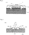
Fig. 2 is a schematic diagram of installation of a semiconductor device to a cooling plate; and -
Fig. 3 is a schematic diagram of a traditional light emitting device. - A jointing material according to a first aspect includes:
- at least one type of element at 0.1wt% to 30wt%, the element being capable of forming a compound with each of tin and carbon; and
- tin at 70wt% to 99.9wt% as a main component.
- Further, as a jointing material of a second aspect, in the first aspect, the jointing material comprises the element at 0.1wt% to 10wt%.
- Further, as a jointing material of a third aspect, in the first aspect or second aspect, the at least one type of element is an element that is more easily oxidized than tin.
- Further, as a jointing material of a fourth aspect, in the any one aspect of first to third aspects, a melting point of a compound of the element with tin is 1,000°C or higher.
- Further, as a jointing material of a fifth aspect, in the any one aspect of first to fourth aspects, the at least one type of element comprises at least one selected from the group consisting of titanium, zirconium, and vanadium.
- A fabrication method for a semiconductor device according to a sixth aspect includes:
- providing a jointing material according to any one aspect of the first to fifth aspect; and
- jointing a light emitting element and a carbon base to each other using the jointing material to fabricate a semiconductor device.
- A semiconductor device according to a seventh aspect includes:
- a light emitting element;
- a carbon base; and
- the jointing material according to any one aspect of the first to fifth aspects, the jointing material jointing the light emitting element and the carbon base to each other.
- Further, a semiconductor device of a eighth aspect, in the seventh aspect, the jointing material comprises the element at a content rate higher than 5wt% and 10wt% or lower.
- A jointing material according to an embodiment will be described with reference to the accompanying drawings. In the drawings, substantially same members are given the same reference numerals.
- A jointing material according to a first embodiment is an alloy that includes an element at 0.1wt% to 30wt%, the element being capable of forming a compound with each of tin and carbon (that is, the element is referred as "compound forming element") and, tin at 70wt% to 99.9wt% as its main component.
- The compound forming element forms a compound with each of tin and carbon, and is not especially limited only when the compound forming element is an element that is more easily oxidized than tin.
- Table 1 is a table of examples of the compounds of each element to be a compound forming element with each of tin, carbon, and oxygen, and the standard Gibbs energy of formation of each of the oxides. The chemical formulae of the compounds however are exemplification and do not represent all the compounds.
[Table 1] Name of Element Compound with Sn Melting Point of Compound with Sn (°C) Compound with C Oxide Standard Gibbs Energy of Formation (kJ/mol) Ti Ti5Sn6 1,490 TiC Ti4O7 -3,213 Y Sn3Y5 515 Y2C Y2O3 -1,817 Nb NbSn2 920 Nb2C Nb2O3 -1,766 Pr PrSn3 1,180 Pr2C3 Pr2O3 -10,674 La LaSn3 1,147 La2C3 LaO3 -1,706 V Sn3V2 1,500 V2C V2O5 -1,420 Mn MnSn2 549 Mn23C6 Mn3O4 -1,283 Th ThSn3 955 ThC ThO2 -1,169 Fe FeSn 513 Fe3C Fe2O3, Fe3O4 -1,016 Zr ZrSn2 1,142 ZrC ZrO2 -1,043 Mo MoSn2 800 MoC MoO3 -668 Li Li2Sn5 326 C6Li Li2O2 -572.7 Sn - - SnO2 -515.7 - As shown in Table 1, examples of the element capable of forming a compound with each of tin and carbon (the compound forming element) include, for example, Ti, Y, Nb, Pr, La, V, Mn, Th, Fe, Zr, Mo, and Li. These elements each form a compound with each of both of tin and carbon and, because the standard Gibbs energy of formation of each of the oxides of these elements is lower than that of the oxide of tin, these elements each more easily form an oxide than tin does even when these elements are each present with tin. The compound forming elements may include at least one selected from the group consisting of titanium, zirconium, and vanadium.
- The reason why titanium, zirconium, and vanadium are selected is that the melting point of each of the compounds with Sn is high as shown in Table 1 (including the melting points are added). The strength of the jointing material is maintained for a longer term as the melting point is higher. The melting point of the compound only has to be at least 1,000°C or higher.
- The compound in a sufficient amount can be formed in the interface between the jointing material and the carbon base and an excellent jointing layer having high strength can be formed in the interface between the carbon base and the jointing material by the fact that the content of the compound forming element of the jointing material is 0.1 wt% or higher.
- The content of the compound forming element may be 5 wt% or higher. An alloy layer grows more and stronger jointing can be established when the content is higher than 5 wt%.
- Tin of a liquid phase component remains and spreads on and wetting the carbon base during the heating when the jointing material and the carbon base are jointed to each other, and excellent jointing without any void is thereby established, by the fact that the content of the compound forming element of the jointing material is 30 wt% or lower.
- It is preferred that the content of the compound forming element be 10 wt% or lower.
- The residual of the jointing material may include only tin. In this case, when the jointing material includes one type of compound forming element, the jointing material is a binary alloy including one type of compound forming element and tin that is the main component.
- The residual of the jointing material may include plural elements including tin that is the main component. In this case, the jointing material is a multi-component alloy including plural elements that includes the compound forming elements and tin that is the main component.
- The content of the elements other than the elements each forming a compound with both of tin and carbon (the compound forming elements) and tin that is the main component is advantageously 0.01 wt% or lower and more advantageously 0.005 wt% or lower. It is preferred that the number of type of the element forming a compound with both of tin and carbon (the compound forming element) be one.
- For example, an ordinary gallium nitride diode can be used as the light emitting element. For example, an n-type gallium nitride and a P-type gallium nitride are formed on the top face of a sapphire substrate, and a P-type electrode and an N-type electrode are formed on the top face thereof to enable electric connection each using a wire. Metalizing (formation of a metal layer) connectable to the jointing material is conducted on the lower face of the sapphire substrate. The metalizing is to form gold to prevent any oxidation, after applying nickel. The metalizing only has to be any element that forms an alloy layer with tin of the jointing material.
- A base produced by forming carbon powder using a casting machine to be sintered is used as the carbon base. The carbon powder is aligned by molding, and the thermal conductivity coefficient in the thickness direction of the carbon base is 600 W/m·K and the thermal conductivity coefficient in the surface direction thereof is 200 W/m·K.
- A jointing article and the production method therefor according to the first embodiment will be described with reference to the drawings.
Fig. 1A to Fig. IF are schematic diagrams of steps of a fabrication method for a semiconductor device according to the first embodiment. - (1) As depicted in
Fig. 1A , ajointing material 101 and acarbon base 102 are first prepared, and are jointed to each other. The jointing conditions are as follows. Thejointing material 101 and thecarbon base 102 are placed in a furnace in a nitrogen atmosphere and are heated up to 1,200°C at a temperature increase rate of 50°C/min. As depicted inFig. 1B , acarbon jointing layer 103 is formed in the interface between thejointing material 101 and thecarbon base 102. Thecarbon jointing layer 103 includes the compound forming element that forms a compound with each of tin and carbon, and is thereby firmly jointed. - (2) As depicted in
Fig. 1C , anelectrode layer 104 is formed. Theelectrode layer 104 is formed to establish electric connection for a light emitting element to be jointed thereto later. Theelectrode layer 104 is bonded to thecarbon base 102 by abonding layer 105 that has an insulation property. - (3) As depicted in
Fig. 1D , thelight emitting element 106 is jointed. The conditions for jointing thelight emitting element 106 and thejointing material 101 to each other are as follows. Thelight emitting element 106 and thecarbon base 102 in the state ofFig. 1C are placed in a furnace in a nitrogen atmosphere and are heated up to 350°C at a temperature increase rate of 50°C/min. The pressure of the inside is reduced to 10 Pa or lower during the heating to remove voids and the pressure is thereafter recovered up to the atmospheric pressure to conduct cooling. Thelight emitting element 106 and thejointing material 101 are thereby jointed to each other.
A light emittingelement jointing layer 107 of nickel·tin formed by a reaction between a nickel-gold layer formed by metalizing on the back face of thelight emitting element 106 and tin of the jointing material 191 is formed in the interface between thejointing material 101 and thelight emitting element 106 after the jointing. - (4)As depicted in Fig. IE, the P-type electrode and the N-type electrode of the
light emitting element 106 are connected to theelectrode layer 104 bywires 108. - (5)As depicted in Fig. IF, the circumference of the
light emitting element 106 is sealed by a sealingresin 109 to fabricate asemiconductor device 110. - The jointing material of this disclosure was produced as described in each of Examples 1 to 12 below. The production conditions and the evaluation results are shown in Table 2.
[Table 2] Jointing Material Compound Forming Element Content of Compound Forming Element (wt%) Temperature of Temperature Measuring Portion (°C) Judgment Example 1 SnTi alloy Ti 0.1 70 • Example 2 SnTi alloy Ti 1 75 • Example 3 SnTi alloy Ti 10 80 • Example 4 SnTi alloy Ti 15 89 ○ Example 5 SnTi alloy Ti 30 97 ○ Example 6 SnV alloy V 0.1 69 • Example 7 SnV alloy V 30 95 ○ Example 8 SnZr alloy Zr 0.1 70 • Example 9 SnZr alloy Zr 30 96 ○ Comparative Example 1 SnTi alloy Ti 0.01 200 × Comparative Example 2 SnTi alloy Ti 35 121 × Comparative Example 3 SnV alloy V 0.01 201 × Comparative Example 4 SnV alloy V 35 119 × Comparative Example 5 SnTi alloy Ti 0.01 199 × Comparative Example 6 SnTi alloy Ti 35 115 × Comparative Example 7 Ag paste - - 201 × - A tin-titanium alloy including titanium at 0.1 wt% and tin at 99.9wt% as the residual was used as the
jointing material 101. Thejointing material 101 had a size of 1 mm×1 mm and a thickness of 0.2 mm as the shape of a molded article thereof. Thecarbon base 102 having a size of 4 mm×4 mm and a thickness of 1 mm was used. - The semiconductor device was fabricated as follows using the jointing material.
- (1) The
jointing material 101 was placed on thecarbon base 102 to be heated to 1,200°C in a furnace and to be cooled. Thejointing material 101 was thereby jointed to thecarbon base 102 by thecarbon jointing layer 103. - (2) The
electrode layer 104 was formed on thecarbon base 102 through thejointing layer 105. The electrode layer included Cu to have a size of 1 mm×2 mm and the thickness: 0.05 mm. - (3) After forming the
electrode layer 104, thelight emitting element 106 having a size of 1 mm×1 mm and a thickness of 0.1 mm was put on thejointing material 101 to be heated at 350°C in a furnace and to be cooled for the jointing to thereby be established. - (4) Electric connection was established by wiring the
aluminum wires 108 between the light emittingelement 106 and theelectrode layer 104. - (5)The
light emitting element 106 was thereafter sealed by the sealingresin 109 to fabricate thesemiconductor device 110. - To check the heat dissipation property after the reliability test, the fabricated
semiconductor device 110 was left untouched in a constant-temperature and constant-humidity bath at a temperature of 85°C and a humidity of 85% for 3,000 hours. - As depicted in
Fig. 2 , acooling plate 201 was thereafter installed beneath thesemiconductor device 110 and the light was caused to be emitted by energization. A thermocouple was installed in a temperature measuring portion T on the surface of the sealingresin 109 in the upper portion of thelight emitting element 106 to conduct the temperature measurement. - It can be seen that the heat did not escape from the lower face of the
light emitting element 106 and was accumulated when the temperature of the surface of the sealingresin 109 was high. - A tin-titanium alloy including titanium at 1 wt% and tin at 99wt% as the residual was used as the
jointing material 101. A semiconductor device was fabricated in the same manner as that of Example 1 for the conditions except the above, and was left untouched in a constant-temperature and constant-humidity bath at a temperature of 85°C and a humidity of 85% for 3,000 hours to thereafter measure the temperature. - A tin-titanium alloy including titanium at 10 wt% and tin at 90wt% as the residual was used as the
jointing material 101. A semiconductor device was fabricated in the same manner as that of Example 1 for the conditions except the above, and was left untouched in a constant-temperature and constant-humidity bath at a temperature of 85°C and a humidity of 85% for 3,000 hours to thereafter measure the temperature. - A tin-titanium alloy including titanium at 15 wt% and tin 85wt% as the residual was used as the
jointing material 101. A semiconductor device was fabricated in the same manner as that of Example 1 for the conditions except the above, and was left untouched in a constant-temperature and constant-humidity bath at a temperature of 85°C and a humidity of 85% for 3,000 hours to thereafter measure the temperature. - A tin-titanium alloy including titanium at 30 wt% and tin 70wt% as the residual was used as the
jointing material 101. A semiconductor device was fabricated in the same manner as that of Example 1 for the conditions except the above, and was left untouched in a constant-temperature and constant-humidity bath at a temperature of 85°C and a humidity of 85% for 3,000 hours to thereafter measure the temperature. - A tin-vanadium alloy including vanadium at 0.1 wt% and tin at 99.9wt% as the residual was used as the
jointing material 101. A semiconductor device was fabricated in the same manner as that of Example 1 for the conditions except the above, and was left untouched in a constant-temperature and constant-humidity bath at a temperature of 85°C and a humidity of 85% for 3,000 hours to thereafter measure the temperature. - A tin-vanadium alloy including vanadium at 30 wt% and tin at 70wt% as the residual was used as the
jointing material 101. A semiconductor device was fabricated in the same manner as that of Example 1 for the conditions except the above, and was left untouched in a constant-temperature and constant-humidity bath at a temperature of 85°C and a humidity of 85% for 3,000 hours to thereafter measure the temperature. - A tin-zirconium alloy including zirconium at 0.1 wt% and tin at 99.9wt% as the residual was used as the
jointing material 101. A semiconductor device was fabricated in the same manner as that of Example 1 for the conditions except the above, and was left untouched in a constant-temperature and constant-humidity bath at a temperature of 85°C and a humidity of 85% for 3,000 hours to thereafter measure the temperature. - A tin-zirconium alloy including zirconium at 30 wt% and tin 70wt% as the residual was used as the
jointing material 101. A semiconductor device was fabricated in the same manner as that of Example 1 for the conditions except the above, and was left untouched in a constant-temperature and constant-humidity bath at a temperature of 85°C and a humidity of 85% for 3,000 hours to thereafter measure the temperature. - A tin-titanium alloy including titanium at 0.01 wt% and tin 99.99wt% as the residual was used as the jointing material. A semiconductor device was fabricated in the same manner as that of Example 1 for the conditions except the above, and was left untouched in a constant-temperature and constant-humidity bath at a temperature of 85°C and a humidity of 85% for 3,000 hours to thereafter measure the temperature.
- A tin-titanium alloy including titanium at 35 wt% and tin 65wt% as the residual was used as the jointing material. A semiconductor device was fabricated in the same manner as that of Example 1 for the conditions except the above, and was left untouched in a constant-temperature and constant-humidity bath at a temperature of 85°C and a humidity of 85% for 3,000 hours to thereafter measure the temperature.
- A tin-vanadium alloy including vanadium at 0.01 wt% and tin at 99.99wt% as the residual was used as the jointing material. A semiconductor device was fabricated in the same manner as that of Example 1 for the conditions except the above, and was left untouched in a constant-temperature and constant-humidity bath at a temperature of 85°C and a humidity of 85% for 3,000 hours to thereafter measure the temperature.
- A tin-vanadium alloy including vanadium at 35 wt% and tin at 65wt% as the residual was used as the jointing material. A semiconductor device was fabricated in the same manner as that of Example 1 for the conditions except the above, and was left untouched in a constant-temperature and constant-humidity bath at a temperature of 85°C and a humidity of 85% for 3,000 hours to thereafter measure the temperature.
- A tin-titanium alloy including titanium at 0.01 wt% and tin at 99.99wt% as the residual was used as the jointing material. A semiconductor device was fabricated in the same manner as that of Example 1 for the conditions except the above, and was left untouched in a constant-temperature and constant-humidity bath at a temperature of 85°C and a humidity of 85% for 3,000 hours to thereafter measure the temperature.
- A tin-titanium alloy including titanium at 35 wt% and tin 65wt% as the residual was used as the jointing material. A semiconductor device was fabricated in the same manner as that of Example 1 for the conditions except the above, and was left untouched in a constant-temperature and constant-humidity bath at a temperature of 85°C and a humidity of 85% for 3,000 hours to thereafter measure the temperature.
- A silver paste was used as the jointing material. A carbon base having a size of 4 mm×4 mm and a thickness of 1 mm was used as the
carbon base 102. - (1) The silver paste was applied to have a thickness of 0.1 mm and a size of 1×1 to the
carbon base 102, and a light emitting element was placed on the applied silver paste for the applied silver paste to be hardened in the atmospheric air at 100°C for 1 hour for bonding therebetween to be established. - (2) An electrode layer was formed on the carbon base through a bonding layer. The electrode layer was Cu and was set to have a size of 1 mm×2 mm and a thickness: 0.05 mm.
- (3) Electric connection was established between the light emitting element and the electrode layer by wiring aluminum wires therebetween.
- (4) The light emitting element was thereafter sealed using the sealing resin to fabricate a semiconductor device.
- To check the heat dissipation property after the reliability test, the fabricated semiconductor device was left untouched in a constant-temperature and constant-humidity bath at a temperature of 85°C and a humidity of 85% for 3,000hours to measure the temperature at the same point as that of Example 1.
- Table 2 shows the fabrication conditions, the temperature measurement result of the surface of the sealing
resin 109, and the judgment result for each of Examples 1 to 9 and Comparative Examples 1 to 6. - The judgment result of the temperature of the surface of the sealing
resin 109 was determined as follows. When the temperature of the surface of the sealingresin 109 was 80°C or lower, it was judged as "•", because degradation of the light emission luminance was very little. When the temperature of the surface of the sealingresin 109 was higher than 80°C to 100°C or lower, it was judged as "○", because degradation of the light emission luminance was little. When the temperature of the surface of the sealingresin 109 was higher than 100°C, it was judged as "×", because degradation of the light emission luminance was conspicuous. - For Examples 1 to 3, the temperatures of the surface of the sealing
resin 109 were 70°C, 75°C, and 80°C to be low temperatures and the judgment for each thereof was "•". It is estimated for this as follows. It can be considered that a tin-titanium-carbon compound was first formed as thecarbon jointing layer 103 in the interface between thecarbon base 102 and the joining material, and a nickel-tin compound was also formed as the light emittingelement jointing layer 107 in the interface between the light emittingelement 106 and thejointing material 101. It can be estimated that the heat-transfer resistance in the interface was therefore reduced different from that of bonding, the heat of thelight emitting element 106 was able to efficiently be transferred to thecarbon base 102, and the heat was caused to escape from thecarbon base 102 having a high thermal conductivity coefficient to thecooling plate 201. - For Examples 4 and 5, the temperatures of the surface of the sealing
resin 109 were 89°C and 97°C, and were 100°C or lower, and the judgment for each thereof was "○". In this case, the heat was also caused to escape similar to the above while, it can be considered that the cooling performance was somewhat degraded compared to those of Examples 1 to 3 because the content of titanium having the thermal conductivity coefficient of 20 W/m·K compared to the thermal conductivity coefficient of 50 W/m·K of tin, was increased. - For Examples 6 and 8 respectively using vanadium and zirconium each as the compound forming element, similarly, the temperatures of the surface of the sealing
resin 109 were 69°C and 70°C to be low temperatures and the judgment for each thereof was "•". For Examples 7 and 9, the temperatures of the surface of the sealingresin 109 were 95°C and 96°C and were 100°C or lower, and the judgment for each thereof was "○". - Similar to the case where titanium was added as the compound forming element, it can be seen for these results that the formation of the compound caused the heat to efficiently escape to the
carbon base 102. On the other hand, it can be estimated that vanadium had the thermal conductivity coefficient of 30 W/m·K and zirconium had the thermal conductivity coefficient of 22.6 W/m·K, and the thermal conductivity coefficient of the jointing layer was reduced when the addition amounts thereof were each increased and the temperatures were each somewhat increased. - For Comparative Examples 1 to 7, the temperatures of the surface of the sealing
resin 109 were all 100°C or higher and the judgment for each thereof was "×". For Comparative Examples 1, 3, and 5, the content of each of titanium, vanadium, and zirconium to be the compound forming elements was 0.01 wt% to be little and it can be estimated that no compound layer was formed in the interface between the carbon base and the jointing material, and any heat transmission was therefore unable to take place resulting in the increase of the temperatures. - For Comparative Examples 2 and 4, the content of each of titanium, vanadium, and zirconium to be the compound forming elements was 30 wt% to be much, the jointing material was therefore not completely melted when the jointing of the light emitting element was conducted, and the voids were not removed for gaps to remain in the jointing layer. It can be estimated that these gaps acted as heat-transfer resistors resulting in no reduction of the temperature.
- The state of the jointing layer was not varied even after 3,000 hours in the constant-temperature and constant-humidity bath at the temperature of 85°C and the humidity of 85% in each of Examples 1 to 9 and Comparative Examples 1 to 6. The side face of the jointing material was analyzed and titanium, vanadium, and zirconium to be the compound forming elements were incrassated as oxides at about 100 nm in the surface layer of the side face. It can be estimated that titanium, vanadium, and zirconium each more easily forming an oxide than tin moved to the surface in which titanium, vanadium, and zirconium were brought into contact with oxygen, by adding titanium, vanadium, and zirconium (the configuration according to a second aspect), and oxides thereof were each formed as a robust oxide layer, and entrance of any oxygen was suppressed into the inside in an amount exceeding a specific amount.
- In Comparative Example 7, because the silver paste was used as the jointing material, oxygen and steam entered the inside of the resin by leaving the semiconductor device untouched for 3,000 hours in the constant-temperature and constant-humidity bath at the temperature of 85°C and the humidity of 85%, the resin was thereby degraded, and gaps were generated therein. The thermal conductivity coefficient was therefore reduced resulting in an increase of the temperature, and the judgment thereof was "×".
- From these results, it can be seen that an alloy including the compound forming element at 0.1 wt% to 30 wt% and tin at 70wt% to 99.9wt% as the residual as its main component is advantageously used as the jointing material. It is preferred that a graphite base and the light emitting element be jointed to each other using this jointing material to fabricate a semiconductor device. The compound forming element of the jointing material is incrassated as an oxide in the interface of the sealing resin of the side face during the leaving untouched at the constant temperature and the constant humidity, the oxide thereby functions as a passive state to suppress advancement of any oxidation, and high reliability can be secured.
- From the results of Examples 1 to 3, it is preferred that the concentration of the compound forming element be 0.1 wt% to 10 wt%. This applies to not only Ti but also V and Zr. This is because Ti, V, and Zr each have lower thermal conductivity than that of Sn and, when a large amount of each thereof is added, the thermal property is degraded.
- This disclosure includes properly combining any optional embodiments and/or Examples with each other of the above various embodiments and/or Examples, and the effects to be achieved by the combined embodiments and/or Examples can be achieved.
- A semiconductor device including a light emitting element and a carbon base that are jointed to each other by the jointing material according to the present invention can secure a high heat dissipation property and high reliability and is usable for a driving current for high luminance.
-
- 101
- jointing material
- 102
- carbon base
- 103
- carbon jointing layer
- 104
- electrode layer
- 105
- bonding layer
- 106
- light emitting element
- 107
- light emitting element jointing layer
- 108
- wire
- 109
- sealing resin
- 110
- semiconductor device
- 201
- cooling plate
- 301
- semiconductor device
- 302
- light emitting element
- 303
- base
- 304
- silver paste
- 305
- electrode
- 306
- wire
- 307
- sealing resin
Claims (8)
- A jointing material comprising:at least one type of element at 0.1wt% to 30wt%, the element being capable of forming a compound with each of tin and carbon; andtin at 70wt% to 99.9wt% as a main component.
- The jointing material according to claim 1, wherein the jointing material comprises the element at 0.1wt% to 10wt%.
- The jointing material according to claim 1, wherein the at least one type of element is an element that is more easily oxidized than tin.
- The jointing material according to claim 1, wherein a melting point of a compound of the element with tin is 1,000°C or higher.
- The jointing material according to claim 1, wherein the at least one type of element comprises at least one selected from the group consisting of titanium, zirconium, and vanadium.
- A fabrication method for a semiconductor device, comprising:providing a jointing material according to claim 1; andjointing a light emitting element and a carbon base to each other using the jointing material to fabricate a semiconductor device.
- A semiconductor device comprising:a light emitting element;a carbon base; andthe jointing material according to claim 1, that joints the light emitting element and the carbon base to each other.
- The jointing material according to claim 1, wherein the jointing material comprises the element at a content rate higher than 5wt% and 10wt% or lower.
Applications Claiming Priority (2)
| Application Number | Priority Date | Filing Date | Title |
|---|---|---|---|
| JP2017229234 | 2017-11-29 | ||
| JP2018144143A JP7108907B2 (en) | 2017-11-29 | 2018-07-31 | Bonding material, method for manufacturing semiconductor device using bonding material, and semiconductor device |
Publications (2)
| Publication Number | Publication Date |
|---|---|
| EP3503227A2 true EP3503227A2 (en) | 2019-06-26 |
| EP3503227A3 EP3503227A3 (en) | 2019-09-04 |
Family
ID=64456845
Family Applications (1)
| Application Number | Title | Priority Date | Filing Date |
|---|---|---|---|
| EP18208056.4A Withdrawn EP3503227A3 (en) | 2017-11-29 | 2018-11-23 | Joining material comprising tin and at least one element capable of forming a compound with each of tin and carbon (titanium, zirconium or vanadium), fabrication method for semiconductor device using the joining material and corresponding semiconductor device |
Country Status (3)
| Country | Link |
|---|---|
| US (1) | US11476399B2 (en) |
| EP (1) | EP3503227A3 (en) |
| CN (1) | CN109834404A (en) |
Citations (1)
| Publication number | Priority date | Publication date | Assignee | Title |
|---|---|---|---|---|
| JP2004265986A (en) | 2003-02-28 | 2004-09-24 | Citizen Electronics Co Ltd | High brightness light emitting element, light emitting device using the same, and method of manufacturing high brightness light emitting element |
Family Cites Families (28)
| Publication number | Priority date | Publication date | Assignee | Title |
|---|---|---|---|---|
| US3361561A (en) | 1964-10-19 | 1968-01-02 | George E Schick | Alloys for soldering conductors to carbon and graphite |
| US3484210A (en) | 1964-10-19 | 1969-12-16 | Henry J Pinter | Alloy coated carbon and graphite members having conductors soldered thereto |
| JPS6340775A (en) | 1986-08-07 | 1988-02-22 | セイコーインスツルメンツ株式会社 | Joining member |
| US5358880A (en) * | 1993-04-12 | 1994-10-25 | Motorola, Inc. | Method of manufacturing closed cavity LED |
| DE19526822C2 (en) | 1995-07-15 | 1998-07-02 | Euromat Gmbh | Solder alloy, use of the solder alloy and method for joining workpieces by soldering |
| JP2000326088A (en) | 1999-03-16 | 2000-11-28 | Nippon Sheet Glass Co Ltd | Lead-free solder |
| CA2340393A1 (en) | 1999-06-11 | 2000-12-21 | Katsuaki Suganuma | Lead-free solder |
| JP2007536088A (en) * | 2004-05-04 | 2007-12-13 | エス−ボンド テクノロジーズ、エルエルシー | Electronic package formed using low-temperature active solder containing indium, bismuth and / or cadmium |
| US7300967B2 (en) * | 2004-11-12 | 2007-11-27 | Eastman Chemical Company | Polyester polymer and copolymer compositions containing metallic titanium particles |
| JP4208863B2 (en) | 2005-06-30 | 2009-01-14 | 富士通マイクロエレクトロニクス株式会社 | Semiconductor device and manufacturing method thereof |
| US20070142511A1 (en) * | 2005-12-15 | 2007-06-21 | Crawford Emmett D | Polyester compositions which comprise cyclobutanediol ethylene glycol, titanium, and phosphorus with improved color and manufacturing processes therefor |
| US7626274B2 (en) | 2006-02-03 | 2009-12-01 | Texas Instruments Incorporated | Semiconductor device with an improved solder joint |
| CN100409996C (en) | 2006-08-28 | 2008-08-13 | 北京航空航天大学 | An oxidation-resistant tin-based lead-free solder capable of flux-free soldering in air |
| JP2008244161A (en) * | 2007-03-27 | 2008-10-09 | Toyoda Gosei Co Ltd | Method for forming electrode of group III nitride compound semiconductor light emitting device |
| TWI361497B (en) * | 2007-08-20 | 2012-04-01 | Delta Electronics Inc | Light-emitting diode apparatus and manufacturing method thereof |
| KR101285958B1 (en) | 2008-10-24 | 2013-07-12 | 미쓰비시덴키 가부시키가이샤 | Solder alloy and semiconductor device |
| US9051435B2 (en) * | 2008-12-16 | 2015-06-09 | The Yokohama Rubber Co., Ltd. | Silanol condensation catalyst, heat-curable silicone resin composition for sealing photosemiconductors and sealed photosemiconductor using same |
| KR101172950B1 (en) | 2009-12-02 | 2012-08-10 | 정경화 | Graphite substrate for light emitting diode and light emitting diode using the same |
| KR101735571B1 (en) * | 2010-08-20 | 2017-05-16 | 삼성전자주식회사 | Thermal dissipation material and light emitting diode package including a junction part made of the thermal dissipation material |
| US11105567B2 (en) | 2012-09-25 | 2021-08-31 | Momentive Performance Materials Quartz, Inc. | Thermal management assembly comprising bulk graphene material |
| GB201312388D0 (en) | 2013-07-10 | 2013-08-21 | Cambridge Entpr Ltd | Materials and methods for soldering and soldered products |
| EP3295081B1 (en) | 2015-05-15 | 2020-07-08 | Momentive Performance Materials Inc. | Light emitting diode assembly using thermal pyrolytic graphite for thermal management |
| JP6516013B2 (en) | 2015-09-17 | 2019-05-22 | 富士電機株式会社 | Solder material for semiconductor devices |
| US20190019911A1 (en) * | 2015-11-24 | 2019-01-17 | PLANT PV, Inc. | Multi-layer metal film stacks for shingled silicon solar cell arrays |
| US20180102464A1 (en) * | 2016-10-06 | 2018-04-12 | Alpha Assembly Solutions Inc. | Advanced Solder Alloys For Electronic Interconnects |
| JP6834424B2 (en) * | 2016-12-02 | 2021-02-24 | 日亜化学工業株式会社 | Semiconductor devices and their manufacturing methods |
| JP6799790B2 (en) | 2016-12-06 | 2020-12-16 | パナソニックIpマネジメント株式会社 | Joining material and the joining body obtained from it and the manufacturing method of the joining body |
| GB201701251D0 (en) * | 2017-01-25 | 2017-03-08 | Univ Oxford Innovation Ltd | A titanium-based alloy |
-
2018
- 2018-11-20 US US16/196,785 patent/US11476399B2/en active Active
- 2018-11-23 EP EP18208056.4A patent/EP3503227A3/en not_active Withdrawn
- 2018-11-26 CN CN201811422049.0A patent/CN109834404A/en active Pending
Patent Citations (1)
| Publication number | Priority date | Publication date | Assignee | Title |
|---|---|---|---|---|
| JP2004265986A (en) | 2003-02-28 | 2004-09-24 | Citizen Electronics Co Ltd | High brightness light emitting element, light emitting device using the same, and method of manufacturing high brightness light emitting element |
Non-Patent Citations (1)
| Title |
|---|
| -: "Significant figures", WIKIPEDIA, 27 October 2017 (2017-10-27), XP055682507, Retrieved from the Internet <URL:https://en.wikipedia.org/w/index.php?title=Significant_figures&oldid=807345766> [retrieved on 20200402] * |
Also Published As
| Publication number | Publication date |
|---|---|
| US11476399B2 (en) | 2022-10-18 |
| EP3503227A3 (en) | 2019-09-04 |
| US20190165234A1 (en) | 2019-05-30 |
| CN109834404A (en) | 2019-06-04 |
Similar Documents
| Publication | Publication Date | Title |
|---|---|---|
| Bajwa et al. | Assembly and packaging technologies for high-temperature and high-power GaN devices | |
| US9066433B2 (en) | Power module substrate, power module substrate with heat sink, power module, and method of manufacturing power module substrate | |
| CN101431038B (en) | Method and paste for multiple metal surface contacting | |
| JP4964009B2 (en) | Power semiconductor module | |
| US20210407953A1 (en) | Solder material for semiconductor device | |
| CN107251246B (en) | Thermoelectric module and method of making the same | |
| JP5871081B2 (en) | BONDED BODY, POWER MODULE SUBSTRATE, POWER MODULE, AND BONDED MANUFACTURING METHOD | |
| KR101758586B1 (en) | Copper/ceramic bond and power module substrate | |
| JP5523680B2 (en) | Bonded body, semiconductor device, and manufacturing method of bonded body | |
| CN101401197A (en) | Electronic component module | |
| KR20090033041A (en) | Methods and pastes for contacting metal surfaces | |
| CN102576975A (en) | Method for thermally contacting opposing electrical connections of a semiconductor component arrangement | |
| US10224472B2 (en) | Thermoelectric power module | |
| US12208448B2 (en) | Transient liquid phase bonding compositions and power electronics assemblies incorporating the same | |
| JP5866075B2 (en) | Bonding material manufacturing method, bonding method, and power semiconductor device | |
| CN101393901A (en) | Semiconductor device | |
| US9343425B1 (en) | Methods for bonding substrates with transient liquid phase bonds by spark plasma sintering | |
| US10886251B2 (en) | Multi-layered composite bonding materials and power electronics assemblies incorporating the same | |
| EP3503227A2 (en) | Joining material comprising tin and at least one element capable of forming a compound with each of tin and carbon (titanium, zirconium or vanadium), fabrication method for semiconductor device using the joining material and corresponding semiconductor device | |
| US10431715B2 (en) | Device and method for producing a device | |
| CN111433910A (en) | Semiconductor device and method of manufacturing the same | |
| JP2022050797A (en) | Ceramics-metal joints and their manufacturing methods, insulated circuit boards, power modules | |
| JP7108907B2 (en) | Bonding material, method for manufacturing semiconductor device using bonding material, and semiconductor device | |
| JP5935517B2 (en) | Brazing material, joining method using brazing material, and semiconductor module | |
| CN108701659A (en) | Bonded body, substrate for power module, power module, method for manufacturing the bonded body, and method for manufacturing substrate for power module |
Legal Events
| Date | Code | Title | Description |
|---|---|---|---|
| PUAI | Public reference made under article 153(3) epc to a published international application that has entered the european phase |
Free format text: ORIGINAL CODE: 0009012 |
|
| AK | Designated contracting states |
Kind code of ref document: A2 Designated state(s): AL AT BE BG CH CY CZ DE DK EE ES FI FR GB GR HR HU IE IS IT LI LT LU LV MC MK MT NL NO PL PT RO RS SE SI SK SM TR |
|
| AX | Request for extension of the european patent |
Extension state: BA ME |
|
| PUAL | Search report despatched |
Free format text: ORIGINAL CODE: 0009013 |
|
| AK | Designated contracting states |
Kind code of ref document: A3 Designated state(s): AL AT BE BG CH CY CZ DE DK EE ES FI FR GB GR HR HU IE IS IT LI LT LU LV MC MK MT NL NO PL PT RO RS SE SI SK SM TR |
|
| AX | Request for extension of the european patent |
Extension state: BA ME |
|
| RIC1 | Information provided on ipc code assigned before grant |
Ipc: H01L 23/373 20060101ALI20190730BHEP Ipc: B23K 35/26 20060101ALI20190730BHEP Ipc: H01L 21/58 20060101ALI20190730BHEP Ipc: H01L 33/64 20100101AFI20190730BHEP |
|
| 17P | Request for examination filed |
Effective date: 20200226 |
|
| RBV | Designated contracting states (corrected) |
Designated state(s): AL AT BE BG CH CY CZ DE DK EE ES FI FR GB GR HR HU IE IS IT LI LT LU LV MC MK MT NL NO PL PT RO RS SE SI SK SM TR |
|
| 17Q | First examination report despatched |
Effective date: 20200409 |
|
| STAA | Information on the status of an ep patent application or granted ep patent |
Free format text: STATUS: THE APPLICATION HAS BEEN WITHDRAWN |
|
| 18W | Application withdrawn |
Effective date: 20200710 |