EP3503179A1 - Electronic device - Google Patents
Electronic device Download PDFInfo
- Publication number
- EP3503179A1 EP3503179A1 EP17209137.3A EP17209137A EP3503179A1 EP 3503179 A1 EP3503179 A1 EP 3503179A1 EP 17209137 A EP17209137 A EP 17209137A EP 3503179 A1 EP3503179 A1 EP 3503179A1
- Authority
- EP
- European Patent Office
- Prior art keywords
- connector
- region
- lead
- formation
- complementary surface
- Prior art date
- Legal status (The legal status is an assumption and is not a legal conclusion. Google has not performed a legal analysis and makes no representation as to the accuracy of the status listed.)
- Withdrawn
Links
Images





Classifications
-
- H—ELECTRICITY
- H10—SEMICONDUCTOR DEVICES; ELECTRIC SOLID-STATE DEVICES NOT OTHERWISE PROVIDED FOR
- H10W—GENERIC PACKAGES, INTERCONNECTIONS, CONNECTORS OR OTHER CONSTRUCTIONAL DETAILS OF DEVICES COVERED BY CLASS H10
- H10W70/00—Package substrates; Interposers; Redistribution layers [RDL]
- H10W70/40—Leadframes
- H10W70/481—Leadframes for devices being provided for in groups H10D8/00 - H10D48/00
-
- H—ELECTRICITY
- H10—SEMICONDUCTOR DEVICES; ELECTRIC SOLID-STATE DEVICES NOT OTHERWISE PROVIDED FOR
- H10W—GENERIC PACKAGES, INTERCONNECTIONS, CONNECTORS OR OTHER CONSTRUCTIONAL DETAILS OF DEVICES COVERED BY CLASS H10
- H10W72/00—Interconnections or connectors in packages
- H10W72/50—Bond wires
-
- H—ELECTRICITY
- H10—SEMICONDUCTOR DEVICES; ELECTRIC SOLID-STATE DEVICES NOT OTHERWISE PROVIDED FOR
- H10W—GENERIC PACKAGES, INTERCONNECTIONS, CONNECTORS OR OTHER CONSTRUCTIONAL DETAILS OF DEVICES COVERED BY CLASS H10
- H10W70/00—Package substrates; Interposers; Redistribution layers [RDL]
- H10W70/40—Leadframes
- H10W70/411—Chip-supporting parts, e.g. die pads
- H10W70/417—Bonding materials between chips and die pads
-
- H—ELECTRICITY
- H10—SEMICONDUCTOR DEVICES; ELECTRIC SOLID-STATE DEVICES NOT OTHERWISE PROVIDED FOR
- H10W—GENERIC PACKAGES, INTERCONNECTIONS, CONNECTORS OR OTHER CONSTRUCTIONAL DETAILS OF DEVICES COVERED BY CLASS H10
- H10W70/00—Package substrates; Interposers; Redistribution layers [RDL]
- H10W70/40—Leadframes
- H10W70/464—Additional interconnections in combination with leadframes
-
- H—ELECTRICITY
- H10—SEMICONDUCTOR DEVICES; ELECTRIC SOLID-STATE DEVICES NOT OTHERWISE PROVIDED FOR
- H10W—GENERIC PACKAGES, INTERCONNECTIONS, CONNECTORS OR OTHER CONSTRUCTIONAL DETAILS OF DEVICES COVERED BY CLASS H10
- H10W70/00—Package substrates; Interposers; Redistribution layers [RDL]
- H10W70/40—Leadframes
- H10W70/464—Additional interconnections in combination with leadframes
- H10W70/466—Tape carriers or flat leads
-
- H—ELECTRICITY
- H10—SEMICONDUCTOR DEVICES; ELECTRIC SOLID-STATE DEVICES NOT OTHERWISE PROVIDED FOR
- H10W—GENERIC PACKAGES, INTERCONNECTIONS, CONNECTORS OR OTHER CONSTRUCTIONAL DETAILS OF DEVICES COVERED BY CLASS H10
- H10W72/00—Interconnections or connectors in packages
-
- H—ELECTRICITY
- H10—SEMICONDUCTOR DEVICES; ELECTRIC SOLID-STATE DEVICES NOT OTHERWISE PROVIDED FOR
- H10W—GENERIC PACKAGES, INTERCONNECTIONS, CONNECTORS OR OTHER CONSTRUCTIONAL DETAILS OF DEVICES COVERED BY CLASS H10
- H10W72/00—Interconnections or connectors in packages
- H10W72/20—Bump connectors, e.g. solder bumps or copper pillars; Dummy bumps; Thermal bumps
-
- H—ELECTRICITY
- H10—SEMICONDUCTOR DEVICES; ELECTRIC SOLID-STATE DEVICES NOT OTHERWISE PROVIDED FOR
- H10W—GENERIC PACKAGES, INTERCONNECTIONS, CONNECTORS OR OTHER CONSTRUCTIONAL DETAILS OF DEVICES COVERED BY CLASS H10
- H10W72/00—Interconnections or connectors in packages
- H10W72/071—Connecting or disconnecting
- H10W72/073—Connecting or disconnecting of die-attach connectors
- H10W72/07331—Connecting techniques
- H10W72/07336—Soldering or alloying
-
- H—ELECTRICITY
- H10—SEMICONDUCTOR DEVICES; ELECTRIC SOLID-STATE DEVICES NOT OTHERWISE PROVIDED FOR
- H10W—GENERIC PACKAGES, INTERCONNECTIONS, CONNECTORS OR OTHER CONSTRUCTIONAL DETAILS OF DEVICES COVERED BY CLASS H10
- H10W72/00—Interconnections or connectors in packages
- H10W72/071—Connecting or disconnecting
- H10W72/076—Connecting or disconnecting of strap connectors
-
- H—ELECTRICITY
- H10—SEMICONDUCTOR DEVICES; ELECTRIC SOLID-STATE DEVICES NOT OTHERWISE PROVIDED FOR
- H10W—GENERIC PACKAGES, INTERCONNECTIONS, CONNECTORS OR OTHER CONSTRUCTIONAL DETAILS OF DEVICES COVERED BY CLASS H10
- H10W72/00—Interconnections or connectors in packages
- H10W72/071—Connecting or disconnecting
- H10W72/076—Connecting or disconnecting of strap connectors
- H10W72/07631—Techniques
- H10W72/07636—Soldering or alloying
-
- H—ELECTRICITY
- H10—SEMICONDUCTOR DEVICES; ELECTRIC SOLID-STATE DEVICES NOT OTHERWISE PROVIDED FOR
- H10W—GENERIC PACKAGES, INTERCONNECTIONS, CONNECTORS OR OTHER CONSTRUCTIONAL DETAILS OF DEVICES COVERED BY CLASS H10
- H10W72/00—Interconnections or connectors in packages
- H10W72/071—Connecting or disconnecting
- H10W72/076—Connecting or disconnecting of strap connectors
- H10W72/07631—Techniques
- H10W72/07637—Techniques using a polymer adhesive, e.g. an adhesive based on silicone or epoxy
-
- H—ELECTRICITY
- H10—SEMICONDUCTOR DEVICES; ELECTRIC SOLID-STATE DEVICES NOT OTHERWISE PROVIDED FOR
- H10W—GENERIC PACKAGES, INTERCONNECTIONS, CONNECTORS OR OTHER CONSTRUCTIONAL DETAILS OF DEVICES COVERED BY CLASS H10
- H10W72/00—Interconnections or connectors in packages
- H10W72/071—Connecting or disconnecting
- H10W72/076—Connecting or disconnecting of strap connectors
- H10W72/07651—Connecting or disconnecting of strap connectors characterised by changes in properties of the strap connectors during connecting
- H10W72/07653—Connecting or disconnecting of strap connectors characterised by changes in properties of the strap connectors during connecting changes in shapes
-
- H—ELECTRICITY
- H10—SEMICONDUCTOR DEVICES; ELECTRIC SOLID-STATE DEVICES NOT OTHERWISE PROVIDED FOR
- H10W—GENERIC PACKAGES, INTERCONNECTIONS, CONNECTORS OR OTHER CONSTRUCTIONAL DETAILS OF DEVICES COVERED BY CLASS H10
- H10W72/00—Interconnections or connectors in packages
- H10W72/60—Strap connectors, e.g. thick copper clips for grounding of power devices
-
- H—ELECTRICITY
- H10—SEMICONDUCTOR DEVICES; ELECTRIC SOLID-STATE DEVICES NOT OTHERWISE PROVIDED FOR
- H10W—GENERIC PACKAGES, INTERCONNECTIONS, CONNECTORS OR OTHER CONSTRUCTIONAL DETAILS OF DEVICES COVERED BY CLASS H10
- H10W72/00—Interconnections or connectors in packages
- H10W72/60—Strap connectors, e.g. thick copper clips for grounding of power devices
- H10W72/631—Shapes of strap connectors
-
- H—ELECTRICITY
- H10—SEMICONDUCTOR DEVICES; ELECTRIC SOLID-STATE DEVICES NOT OTHERWISE PROVIDED FOR
- H10W—GENERIC PACKAGES, INTERCONNECTIONS, CONNECTORS OR OTHER CONSTRUCTIONAL DETAILS OF DEVICES COVERED BY CLASS H10
- H10W72/00—Interconnections or connectors in packages
- H10W72/60—Strap connectors, e.g. thick copper clips for grounding of power devices
- H10W72/631—Shapes of strap connectors
- H10W72/634—Cross-sectional shape
-
- H—ELECTRICITY
- H10—SEMICONDUCTOR DEVICES; ELECTRIC SOLID-STATE DEVICES NOT OTHERWISE PROVIDED FOR
- H10W—GENERIC PACKAGES, INTERCONNECTIONS, CONNECTORS OR OTHER CONSTRUCTIONAL DETAILS OF DEVICES COVERED BY CLASS H10
- H10W72/00—Interconnections or connectors in packages
- H10W72/851—Dispositions of multiple connectors or interconnections
- H10W72/874—On different surfaces
- H10W72/886—Die-attach connectors and strap connectors
-
- H—ELECTRICITY
- H10—SEMICONDUCTOR DEVICES; ELECTRIC SOLID-STATE DEVICES NOT OTHERWISE PROVIDED FOR
- H10W—GENERIC PACKAGES, INTERCONNECTIONS, CONNECTORS OR OTHER CONSTRUCTIONAL DETAILS OF DEVICES COVERED BY CLASS H10
- H10W90/00—Package configurations
- H10W90/701—Package configurations characterised by the relative positions of pads or connectors relative to package parts
- H10W90/731—Package configurations characterised by the relative positions of pads or connectors relative to package parts of die-attach connectors
- H10W90/736—Package configurations characterised by the relative positions of pads or connectors relative to package parts of die-attach connectors between a chip and a stacked lead frame, conducting package substrate or heat sink
-
- H—ELECTRICITY
- H10—SEMICONDUCTOR DEVICES; ELECTRIC SOLID-STATE DEVICES NOT OTHERWISE PROVIDED FOR
- H10W—GENERIC PACKAGES, INTERCONNECTIONS, CONNECTORS OR OTHER CONSTRUCTIONAL DETAILS OF DEVICES COVERED BY CLASS H10
- H10W90/00—Package configurations
- H10W90/701—Package configurations characterised by the relative positions of pads or connectors relative to package parts
- H10W90/761—Package configurations characterised by the relative positions of pads or connectors relative to package parts of strap connectors
- H10W90/766—Package configurations characterised by the relative positions of pads or connectors relative to package parts of strap connectors between a chip and a stacked lead frame, conducting package substrate or heat sink
Definitions
- the invention relates to an electronic device.
- the present invention relates to a connector, or clip, for connecting a die to a lead in an electronic device.
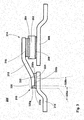
- Fig. 1a shows a cross-sectional view of a portion of an electronic device 100, for example a semiconductor device, comprising die support 102, electronic die (e.g., semiconductor chip) 104, connector, or clip, 106 and a lead 108 of a leadframe.
- die support 102 electronic die (e.g., semiconductor chip) 104
- connector e.g., connector
- clip e.g., connector
- leadframe e.g., a leadframe
- Die 104 is attached to die support 102 by bonding material 110.
- Contact 112 on die 104 is bonded to a die-end 114 of connector 106 by an electrically conductive bonding material 116, such as, for example, solder, sinter materials, conductive glue, or the like.
- a lead-end 118 of connector 106 is bonded to a connector-pad 120, which comprises a planar region of lead 108, by electrically conductive bonding material 122 that may, again, comprise solder, sinter materials, conductive glue, or the like.
- a portion of the lead-end 118 of connector 106 adjacent the connector-pad 120 is generally flat.
- solder joint does not comprise a so-called “dry-joint” or “cold-solder joint” so as to ensure good electrical conduction between joined parts. Any defect in a solder joint can lead to a joint that is non-functional either immediately or after a period of use.
- a surface at a solder-atmosphere interface of a fillet of solder formed around a region where two parts to be joined meet is concave. Presence of a concave surface can reduce stress concentration at the surface of a solder joint, which may reduce the possibility of cracks forming in the solder and propagating through the solder.
- One known example comprises temperature cycle testing, which comprises a process of cycling through temperature extremes, typically at relatively high rates of change to evaluate product reliability.
- a concave surface of electrically conductive bonding material 122 is formed at a first end 124a of the connector-connector pad interface.
- a first article inspection revealed that a similar shaped surface is not formed at a second end 124b of the connector-connector pad interface, which is influenced by the shape of the end of the connector 16. That is, the joint is not symmetric.
- TCT thermal cycling test
- the joint failed after 1000 cycles due to a mismatch in the coefficients of thermal expansion of the electrically conductive bonding material, e.g. an epoxy moulding compound, and the connector-pad 120 of lead 108. Failure was caused by a crack, which formed in the electrically conductive bonding material 122 at the second end 124b of the connector-connector pad interface, propagating through the electrically conductive bonding material 122.
- a die-attach and clip-attach (DACA) process is optimised to provide a greater volume of solder on the connector-pad.
- possibility of solder crack occurring is still limited by shape and/or configuration of an end of connector 106.
- joint failure occurred after 2000 cycles in a TCT.
- an electronic device comprising: a die; at least one lead; a corresponding at least one connector, the or each connector for connecting the die to a corresponding lead or leads, and the or each connector comprising a first end disposed in bondable proximity to a complementary surface of the corresponding lead and a second end disposed in bondable proximity to a complementary surface of the die; wherein an end portion of at least one of the first end and second end comprises a formation, the formation in combination with the complementary surface of one, or both, of the respective lead or the die defining therebetween a first region and at least a second region configured to attract by capillary action an electrically conductive bonding material to consolidate therein.
- Such an electronic device may comprise bonding material of greater thickness, or volume, between connector and connector-pad (i.e. lead-end or on die), compared with known arrangements, while also keeping the overall footprint the same. This may increase the strength of the bonding joint, compared with known arrangements, because the bonding joint contains more bonding material and the elastic and plastic deformation during thermo-mechanic stresses may be reduced. Formation of a concave surface at a solder-atmosphere interface of a fillet of solder formed around a region where two parts to be joined meet may be promoted using a connector according to the present invention. Presence of a concave surface can reduce stress concentration at the surface of a solder joint, which may reduce the possibility of cracks forming in the solder and propagating through the solder.
- the formation at said first end may comprise a bend out of a plane of the connector such that a portion of the end portion of the first end extends in a direction out of the plane of the connector.
- the end portion of the first end may extend in a direction out of the plane of the connector away from the lead.
- the electronic device may further comprise a third region, wherein said second region and third region are located on either side of said first region, and further where said first region is partially defined by an apex of said bend and a portion of said complementary surface of said lead opposing said apex, said second region is partially defined by a first portion of said connector adjacent said apex and a portion of said complementary surface of said lead opposing said first portion, and said third region is partially defined by a second portion of said connector adjacent said apex and a portion of said complementary surface of said lead opposing said second portion.
- the formation at said first end may comprise a step formed in a tip of the first end, the step extending at least partly across a width of the first end, and further wherein said second region is partially defined by a first part of said step and a portion of said complementary surface of said lead opposing said first part, and said first region is partially defined by a second part of said step and a portion of said complementary surface of said lead opposing said second part.
- the formation at said first end may comprise peaks with a channel therebetween, said peaks and channel in a surface of the first end opposing the complementary surface of the corresponding lead and extending at least partly across a length of the first end, and further wherein said second region is partially defined by said channel and a portion of said complementary surface of said lead opposing said channel, and said first region is partially defined by said peaks and portions of said complementary surface of said lead opposing said peaks.
- the formation at said first end may comprise a bend out of a plane of the connector such that a first portion of the end region of the first end extends in a direction out of a plane of the connector toward the lead and a second portion of the end region of the first end, remote from the second end, extends in a direction out of a plane of the first portion away from the lead.
- the formation at said second end comprises a bend out of a plane of the connector such that a portion of the end region of the second end extends in a direction out of the plane of the connector.
- the end region of the second end may extend in a direction out of the plane of the connector away from the die.
- the electronic device may further comprise a third region, wherein said second region and third region are located on either side of said first region, and further where said first region is partially defined by an apex of said bend and a portion of said complementary surface of said die opposing said apex, said second region is partially defined by a first portion of said connector adjacent said apex and a portion of said complementary surface of said die opposing said first portion, and said third region is partially defined by a second portion of said connector adjacent said apex and a portion of said complementary surface of said die opposing said second portion.
- the formation at said second end may comprise a step formed in a tip of the second end, the step extending at least partly across a width of the second end, and further wherein said second region is partially defined by a first part of said step and a portion of said complementary surface of said die opposing said first part, and said first region is partially defined by a second part of said step and a portion of said complementary surface of said die opposing said second part.
- the formation at said second end may comprise peaks with a channel therebetween, said peaks and channel formed in a surface of the second end opposing the complementary surface of the corresponding lead and extending at least partly across a length of the second end, and further wherein said second region is partially defined by said channel and a portion of said complementary surface of said die opposing said channel, and said first region is partially defined by said peaks and portions of said complementary surface of said die opposing said peaks.
- the formation at said second end may comprise a bend out of a plane of the connector such that a first portion of the end region of the second end extends in a direction out of a plane of the connector toward the die and a second portion of the end region of the second end, remote from the first end, extends in a direction out of a plane of the first portion away from the die.
- the electronic device may comprise a power rectifier device or a transient voltage suppression device.
- a connector for use in an electronic device as described above and hereinafter, the connector for connecting a die to a lead of the electronic device, the connector comprising a first end for disposition in bondable proximity to a complementary surface of the lead, and a second end for disposition in bondable proximity to a complementary surface of the die, wherein an end portion of at least one of the first and second ends comprises a formation, the formation in combination with the complementary surface of one, or both, of the respective lead or the die defining therebetween a first region and at least a second region configured to attract by capillary action an electrically conductive bonding material to consolidate therein.
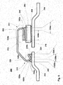
- Fig. 2 which illustrates a cross-section view of a portion of an electronic device 200 according to one or more embodiments of the present invention
- die 202 having contact 204 is mounted on a die support 206 by bonding material 208.
- the bonding material 208 may be conductive or insulating, but an electrically conductive bonding material is frequently used when die support 206 is also intended to serve as one of the electrical leads of the device coupled to die 202.
- Lead 210 is provided extending toward die 202 and is configured to serve as an external connection to die 202.
- Connector, or clip, 212 extends from lead 210 to the contact 204 on die 202.
- a die-end 214 of connector 212 is attached to contact 204 of die 202 by electrically conductive bonding material 216.
- a lead-end 218 of connector 212 is attached to lead 210 by electrically conductive bonding material 220.
- An electrically conductive solder is an example of a suitable electrically conductive bonding material.
- the type of electrically conductive bonding materials 216, 220 employed should be capable of being liquefied, in order to flow in an unset state (e.g. when heated), and further capable of hardening to a set state.
- the electrically conductive bonding materials 216, 220 have a common liquification or melting temperature so that they be temporarily, at least partially, liquid at the same time during a period of the bonding process. That is, it is desirable that the electrically conductive bonding materials 216, 220 have a common state, e.g., a temperature range or curing or bonding condition or the like, where they are semi-solid or at least partially liquid.
- the electrically conductive bonding materials 216, 220 should be sufficiently liquid that the connector 212 can float on the electrically conductive bonding material 216, 220 when the electrically conductive bonding material 216, 220 is in a semi-solid, partially liquid, or liquid state, and be free to move with respect to die 202 and lead 210 so as to "sink" into the electrically conductive bonding material 216, 220.
- the electrically conductive bonding materials 216, 220 are temporarily liquefied, or temporarily maintained as liquids, to permit connector 212 to float on liquified electrically conductive bonding materials 216, 220, so that the connector 212, die 202 and lead 210 self-align by surface tension.
- a material of the electrically conductive bonding material 216, 220 should be capable of flowing in order to readily wet the ends of the connector 212 and respective complementary surfaces of the die 202 and the lead 210.
- the complementary surface of the die 202 comprises contact 204 and the complementary surface of the lead 210 comprises a connector-pad 224 region of lead 210.
- the lead-end 218 of connector 212 comprises a bend formation 226.
- the bend formation 226 in combination with the complementary surface defined by connector-pad 224 of lead 210 define therebetween a region into which the electrically conductive bonding material 220 can flow (when in a liquid state) and harden.
- the arrangement of the bend formation 226 and opposing portion of the complementary surface serves to attract, by capillary action, the electrically conductive bonding material 220 into the region therebetween. This causes the electrically conductive bonding material 220, when in a liquid state, to flow into the space and consolidate around the bend formation 226 and the complementary surface defined by connector-pad 224.
- the bend formation 226 comprises a bend out of a plane of the connector 212 such that a portion of the lead-end 218 extends in a direction out of the plane of the connector 212 away from the lead 210.
- a volume partially bounded by the bend formation 226 and a portion of the complementary surface defined by the connector-pad 224 that opposes the bend formation 226 comprises three regions. These three regions comprise: a first region 228a partially defined by an apex 226a of the bend formation 226 and a portion of the complementary surface of the lead 210 opposing the apex; a second region 228b partially defined by a first portion 226b of the connector 212 adjacent the apex 226a and a portion of the complementary surface of the lead opposing the first portion 226b; and a third region 228c partially defined by a second portion 226c of the connector adjacent the apex 226a and a portion of the complementary surface of the lead opposing the second portion 226c.
- Increasing the thickness, or volume, of bonding material between connector and connector-pad, while keeping the overall footprint the same may increase the strength of the bonding joint, because the bonding joint contains more bonding material and the elastic and plastic deformation during thermo-mechanic stresses may be reduced.
- Fig. 1b illustrates simulation data that shows accumulated plastic strain of a bonding material (i.e. solder in the illustrated data) between a connector and a connector-pad for a known connector (such as that illustrated in Fig. 1a ) and for a connector according to one or more embodiments of the present invention (e.g. as illustrated in Fig. 2 ). From the figure, it can be seen that accumulated plastic strain of solder at an end of the connector according to one or more embodiments of the invention (e.g. that illustrated in Fig. 2 ) is about 25% lower than that for the known connector (i.e. as shown in Fig. 1 ) under TCT.
- the data indicates that the design of the connector end of Fig. 2 may potentially pass 2500 TCT cycles (c.f. with a known connector, which can marginally pass 2000 TCT cycles).
- configuring a surface of the connector that is to oppose the connector-pad so that larger volume regions are formed between connector and connector-pad can increase the volume of the bonding joint, but keep the footprint of the joint the same.
- the formation 226 illustrated in Fig. 2 may promote formation of concave surfaces 230a, 230b at the bonding material-atmosphere interface on both sides of the bonding joint.
- the bonding joint is generally symmetric.
- the formation 226 that achieves this in the arrangement illustrated in Fig. 2 comprises a bend in the connector 210.
- the formation may comprise recesses, channels, steps and/or other surface features that achieve a non-flat surface of the connector that is to face the connector-pad. Examples of these other features are described further below with reference to Figs. 3 to 6 .
- Fig. 3 illustrates an electronic device 200 according to one or more embodiments of the present invention in which another type of formation is employed.
- Features illustrated in Fig. 3 that are common to the electronic device 200 illustrated in Fig. 2 (and as described above) are denoted using like reference numerals.
- the lead-end 218 of connector 212 comprises a step formation 326.
- the step formation 326 in combination with the complementary surface defined by connector-pad 224 of lead 210 define therebetween a region into which the electrically conductive bonding material 220 can flow (when in a liquid state) and harden.
- the arrangement of the step formation 326 and opposing portion of the complementary surface defined by connector-pad 224 serves to attract, by capillary action, the electrically conductive bonding material 220 into the region therebetween. This causes the electrically conductive bonding material 220, when in a liquid state, to flow into the space and consolidate around the step formation 326 and the complementary surface defined by connector-pad 224.
- the step formation 326 comprises a step formed at a tip of the lead-end 218 so that an overhang 326a is formed with a recess below.
- a spacing between the overhang 326a and the connector-pad 224 is greater than a spacing between the connector-pad 224 and a portion 326b of the connector 212 toward a die-end 214 of connector 212.
- the overhang 326a and recess extend across the width of the tip of the lead-end 218 of connector 212.
- a volume partially bounded by the step formation 326 and a portion of the complementary surface defined by the connector-pad 224 that opposes the step formation 326 comprises two regions. These two regions comprise: a first region 328a partially defined by the overhang 326a of the step formation 326 and a portion of the complementary surface of the lead 210 opposing the overhang 326a; and a second region 328b partially defined by the portion 326b of the connector 212 and a portion of the complementary surface of the lead opposing the portion 326b.
- the step formation 326 of the electronic device 200 illustrated in Fig. 3 provides a surface of the connector that is to oppose the connector-pad that, in combination with the complementary surface of the connector-pad, defines larger volume regions between connector and connector-pad (compared with previous "flat" arrangements e.g. as illustrated in Fig. 1a ). This can increase the volume of the bonding joint, but keep the footprint of the joint the same.
- the step formation 326 of Fig. 3 may promote formation of concave surfaces 230a, 230b at the bonding material-atmosphere interface on both sides of the bonding joint. Again, this may lead to a bonding joint that is generally symmetric.
- Figs. 4a to 4c illustrate an electronic device 200 according to one or more embodiments of the present invention in which another type of formation is employed.
- Features illustrated in Fig. 4a to 4c that are common to the electronic devices 200 illustrated in Figs. 2 and 3 (and as described above) are denoted using like reference numerals.
- the lead-end 218 of connector 212 comprises a channel formation 426.
- the channel formation 426 in combination with the complementary surface defined by connector-pad 224 of lead 210 define therebetween a region into which the electrically conductive bonding material 220 can flow (when in a liquid state) and harden.
- the arrangement of the channel formation 426 and opposing portion of the complementary surface defined by connector-pad 224 serves to attract, by capillary action, the electrically conductive bonding material 220 into the region therebetween. This causes the electrically conductive bonding material 220, when in a liquid state, to flow into the space and consolidate around the channel formation 426 and the complementary surface defined by connector-pad 224.
- the channel formation 426 comprises a channel 426a formed between first and second peaks 426b, 426c.
- the channel 426a and peaks 426b, 426c are formed in a surface of the lead-end 218 that is to oppose the connector-pad 224.
- the channel 426a and peaks 426b, 426c extend along a length of the surface of the lead-end 218, i.e. in a direction from a tip of the lead-end 218 toward a die-end 214 of the connector 212.
- a spacing between a base of the channel 426a and the connector-pad 224 is greater than a spacing between the peaks 426b, 426c and the connector-pad 224.
- a volume partially bounded by the channel formation 426 and a portion of the complementary surface defined by the connector-pad 224 that opposes the channel formation 426 comprises three regions. These three regions comprise: a first region 428a partially defined by the channel 426a and a portion of the complementary surface of the lead 210 opposing the channel 426a; a second region 428b partially defined by a first peak 426b of the channel formation 426 and a portion of the complementary surface of the lead 210 opposing the first peak 426b; and a third region 428c partially defined by a second peak 426c and a portion of the complementary surface of the lead 210 opposing the second peak 426c.
- the channel formation 426 of the electronic device 200 illustrated in Figs. 4a to 4c provides a surface of the connector that is to oppose the connector-pad that, in combination with the complementary surface of the connector-pad, defines larger volume regions between connector and connector-pad (compared with previous "flat" arrangements e.g. as illustrated in Fig. 1a ). This can increase the volume of the bonding joint, but keep the footprint of the joint the same.
- the channel formation 426 of Figs. 4a to 4c may promote formation of concave surfaces 230a, 230b at the bonding material-atmosphere interface on both sides of the bonding joint.
- the bonding joint may be generally symmetric.
- Fig. 5 illustrates an electronic device 200 according to one or more embodiments of the present invention in which other types of formation are employed.
- Features illustrated in Fig. 5 that are common to the electronic devices 200 illustrated in Figs. 2 , 3 , and 4a to 4c (and as described above) are denoted using like reference numerals.
- the lead-end 218 of connector 212 comprises a first bend formation 526. Also, the die-end 214 of connector 212 comprises a second bend formation 532.
- the first bend formation 526 in combination with the complementary surface defined by connector-pad 224 of lead 210 define therebetween a region into which the electrically conductive bonding material 220 can flow (when in a liquid state) and harden.
- the arrangement of the bend formation 526 and opposing portion of the complementary surface serves to attract, by capillary action, the electrically conductive bonding material 220 into the region therebetween. This causes the electrically conductive bonding material 220, when in a liquid state, to flow into the space and consolidate around the bend formation 526 and the complementary surface defined by connector-pad 224.
- the second bend formation 532 in combination with the complementary surface defined by contact 204 of die 202 define therebetween a region into which the electrically conductive bonding material 216 can flow (when in a liquid state) and harden.
- the arrangement of the second bend formation 532 and opposing portion of the complementary surface serves to attract, by capillary action, the electrically conductive bonding material 216 into the region therebetween. This causes the electrically conductive bonding material 216, when in a liquid state, to flow into the space and consolidate around the second bend formation 532 and the complementary surface defined by contact 204.
- the first bend formation 526 comprises a first portion of an end region of the lead-end 218 that extends in a direction out of a plane of the connector toward the lead 210 and a second portion of the end region of the lead-end 218, remote from the die-end 214, which extends in a direction out of a plane of the first portion away from the lead 210.
- the second bend formation 532 comprises a first portion of an end region of the die-end 214 that extends in a direction out of a plane of the connector toward the contact 204 and a second portion of the end region of the die-end 214, remote from the lead-end 218, which extends in a direction out of a plane of the first portion.
- a volume partially bounded by the first bend formation 526 and a portion of the complementary surface defined by the connector-pad 224 that opposes the bend formation 526 comprises three regions. These three regions comprise: a first region 528a partially defined by an apex 526a of the first bend formation 526 and a portion of the complementary surface of the lead 210 opposing the apex 526a; a second region 528b partially defined by a first portion 526b of the connector 212 adjacent the apex 526a and a portion of the complementary surface of the lead opposing the first portion 526b; and a third region 528c partially defined by a second portion 526c of the connector adjacent the apex 526a and a portion of the complementary surface of the lead 210 opposing the second portion 526c.
- the first bend formation 526 of the electronic device 200 illustrated in Fig. 5 provides a surface of the connector that is to oppose the connector-pad that, in combination with the complementary surface of the connector-pad, defines larger volume regions between connector and connector-pad (compared with previous "flat" arrangements e.g. as illustrated in Fig. 1a ). This can increase the volume of the bonding joint, but keep the footprint of the joint the same.
- the first bend formation 526 of Fig. 5 may promote formation of concave surfaces 230a, 230b at the bonding material-atmosphere interface on both sides of the bonding joint.
- the bonding joint may be generally symmetric.
- a volume partially bounded by the second bend formation 532 and a portion of the complementary surface defined by the contact 204 that opposes the second bend formation 532 comprises two regions. These two regions comprise: a first region 534a partially defined by a first portion 532a of the connector 212 (between the apex of the bend and a second portion 532b of the connector toward the tip of the connector 212 at the die-end 214) and a portion of the complementary surface of the contact 204 opposing the first portion 532a; and a second region 534b partially defined by the second portion 532b of the connector 212 and a portion of the complementary surface of the contact 204 opposing the second portion 532b.
- the second bend formation 532 of the electronic device 200 illustrated in Fig. 5 provides a surface of the connector that is to oppose the contact 204 that, in combination with the complementary surface of the contact 204, defines larger volume regions between connector and contact 204 (compared with previous "flat" arrangements e.g. as illustrated in Fig. 1a ). This can increase the volume of the bonding joint, but keep the footprint of the joint the same.
- the second bend formation 532 of Fig. 5 may promote formation of concave surfaces at the bonding material-atmosphere interface on both sides of the bonding joint.
- the bonding joint may be generally symmetric.
- Fig. 6 illustrates an electronic device 200 according to one or more embodiments of the present invention in which other types of formation are employed.
- Features illustrated in Fig. 6 that are common to the electronic devices 200 illustrated in Figs. 2 , 3 , 4a to 4c and 5 (and as described above) are denoted using like reference numerals.
- the lead-end 218 of connector 212 comprises a first bend formation 626. Also, the die-end 214 of connector 212 comprises a second bend formation 632.
- the first bend formation 626 in combination with the complementary surface defined by connector-pad 224 of lead 210 define therebetween a region into which the electrically conductive bonding material 220 can flow (when in a liquid state) and harden.
- the arrangement of the first bend formation 626 and opposing portion of the complementary surface serves to attract, by capillary action, the electrically conductive bonding material 220 into the region therebetween. This causes the electrically conductive bonding material 220, when in a liquid state, to flow into the space and consolidate around the first bend formation 626 and the complementary surface defined by connector-pad 224.
- the second bend formation 632 in combination with the complementary surface defined by contact 204 of die 202 define therebetween a region into which the electrically conductive bonding material 216 can flow (when in a liquid state) and harden.
- the arrangement of the second bend formation 632 and opposing portion of the complementary surface serves to attract, by capillary action, the electrically conductive bonding material 216 into the region therebetween. This causes the electrically conductive bonding material 216, when in a liquid state, to flow into the space and consolidate around the second bend formation 632 and the complementary surface defined by contact 204.
- the first bend formation 626 comprises a first portion of an end region of the lead-end 218 that extends in a direction out of a plane of the connector toward the lead 210 and a second portion of the end region of the lead-end 218, remote from the die-end 214, which extends in a direction out of a plane of the first portion away from the lead 210.
- the second bend formation 632 comprises a first portion of an end region of the die-end 214 that extends in a direction out of a plane of the connector toward the contact 204 and a second portion of the end region of the lead-end 218, remote from the lead-end 218, which extends in a direction out of a plane of the first portion away from the contact 204.
- a volume partially bounded by the first bend formation 626 and a portion of the complementary surface defined by the connector-pad 224 that opposes the first bend formation 626 comprises three regions. These three regions comprise: a first region 628a partially defined by an apex 626a of the first bend formation 626 and a portion of the complementary surface of the lead 210 opposing the apex 626a; a second region 628b partially defined by a first portion 626b of the connector 212 adjacent the apex 626a and a portion of the complementary surface of the lead opposing the first portion 626b; and a third region 628c partially defined by a second portion 626c of the connector adjacent the apex 626a and a portion of the complementary surface of the lead 210 opposing the second portion 626c.
- the first bend formation 626 of the electronic device 200 illustrated in Fig. 6 provides a surface of the connector that is to oppose the connector-pad that, in combination with the complementary surface of the connector-pad, defines larger volume regions between connector and connector-pad (compared with previous "flat" arrangements e.g. as illustrated in Fig. 1a ). This can increase the volume of the bonding joint, but keep the footprint of the joint the same.
- the first bend formation 626 of Fig. 6 may promote formation of concave surfaces 230a, 230b at the bonding material-atmosphere interface on both sides of the bonding joint. Again, the bonding part is generally symmetric.
- a volume partially bounded by the second bend formation 632 and a portion of the complementary surface defined by the contact 204 that opposes the second bend formation 632 comprises three regions. These three regions comprise: a first region 634a partially defined by an apex 632a of the second bend formation 632 and a portion of the complementary surface of the contact 204 opposing the apex 632a; a second region 634b partially defined by a first portion 632b of the connector 212 adjacent the apex 632a and a portion of the complementary surface of the contact 204 opposing the first portion 632b; and a third region 634c partially defined by a second portion 632c of the connector adjacent the apex 632a and a portion of the complementary surface of the contact 204 opposing the second portion 632c.
- the second bend formation 632 of the electronic device 200 illustrated in Fig. 6 provides a surface of the connector that is to oppose the contact 204 that, in combination with the complementary surface of the contact 204, defines larger volume regions between connector and contact 204 (compared with previous "flat" arrangements e.g. as illustrated in Fig. 1a ). This can increase the volume of the bonding joint, but keep the footprint of the joint the same.
- the second bend formation 632 of Fig.6 may promote formation of concave surfaces at the bonding material-atmosphere interface on both sides of the bonding joint. Again, the bonding joint is generally symmetric.
- the lead-end 218 of connector 212 comprises a formation 226, 326, 426, 526, 626.
- the die-end 214 of connector 212 may comprise a formation 532, 632.
- both the lead-end 218 and die-end 214 of connector may comprise a formation.
- a lead-end of a connector may be provided with a formation of at least one of the types described above.
- a die-end of a connector may be provided with a formation of at least one of the types described above.
- the formations may be of a same type, or a different type at each end.
- the lead-end 218 of connector 212 comprises a step formation 326 in which the overhang 326a and recess extend across the width of the tip of the lead-end 218 of connector 212.
- the overhang 326a and recess extend partially across the width of the tip of the lead-end 218 of connector 212.
- the lead-end 218 of connector 212 comprises a channel formation 426 in which the channel 426a and peaks 426b, 426c extend across an entire length of the surface of the lead-end 218 that is to oppose the connector-pad 224.
- the channel 426a and peaks 426b, 426c extend partially across the length of the surface of the lead-end 218 that is to oppose the connector-pad 224.
- the bend formation may comprise a J-bend or a V-bend.
Landscapes
- Connections Effected By Soldering, Adhesion, Or Permanent Deformation (AREA)
- Details Of Connecting Devices For Male And Female Coupling (AREA)
- Coupling Device And Connection With Printed Circuit (AREA)
Abstract
There is disclosed an electronic device comprising a die and at least one lead. The electronic device further comprises a corresponding at least one connector (212), the or each connector for connecting the die (202) to a corresponding lead or leads (210), and the or each connector (212) comprising a first end (218) disposed in bondable proximity to a complementary surface of the corresponding lead (210) and a second end (214) disposed in bondable proximity to a complementary surface of the die (202). An end portion of at least one of the first end (218) and second end (214) comprises a formation (226, 326, 426), the formation (226, 326, 426) in combination with the complementary surface (224) of one, or both, of the respective lead (210) or the die (202) defining therebetween a first region (228a, 328a, 428a) and at least a second region (228b, 328b, 428b) configured to attract by capillary action an electrically conductive bonding material to consolidate therein. There is also disclosed a connector for use in an electronic device.
Description
- The invention relates to an electronic device. In particular, but not exclusively, the present invention relates to a connector, or clip, for connecting a die to a lead in an electronic device.
-
Fig. 1a shows a cross-sectional view of a portion of anelectronic device 100, for example a semiconductor device, comprising diesupport 102, electronic die (e.g., semiconductor chip) 104, connector, or clip, 106 and alead 108 of a leadframe. - Die 104 is attached to die
support 102 bybonding material 110. Contact 112 on die 104 is bonded to a die-end 114 ofconnector 106 by an electricallyconductive bonding material 116, such as, for example, solder, sinter materials, conductive glue, or the like. - A lead-
end 118 ofconnector 106 is bonded to a connector-pad 120, which comprises a planar region oflead 108, by electricallyconductive bonding material 122 that may, again, comprise solder, sinter materials, conductive glue, or the like. - A portion of the lead-
end 118 ofconnector 106 adjacent the connector-pad 120 is generally flat. - In electronic devices, it is essential that a solder joint does not comprise a so-called "dry-joint" or "cold-solder joint" so as to ensure good electrical conduction between joined parts. Any defect in a solder joint can lead to a joint that is non-functional either immediately or after a period of use. Ideally a surface at a solder-atmosphere interface of a fillet of solder formed around a region where two parts to be joined meet is concave. Presence of a concave surface can reduce stress concentration at the surface of a solder joint, which may reduce the possibility of cracks forming in the solder and propagating through the solder.
- Techniques have been developed to mimic the stresses that a solder joint will undergo during a period of use and these techniques employ repeated stressing and de-stressing of a component to induce failure through fatigue. One known example comprises temperature cycle testing, which comprises a process of cycling through temperature extremes, typically at relatively high rates of change to evaluate product reliability.
- In the prior art arrangement illustrated in
Fig. 1a , a concave surface of electricallyconductive bonding material 122 is formed at afirst end 124a of the connector-connector pad interface. However, a first article inspection revealed that a similar shaped surface is not formed at asecond end 124b of the connector-connector pad interface, which is influenced by the shape of the end of the connector 16. That is, the joint is not symmetric. - In a thermal cycling test (TCT) of a joint of electrically
conductive bonding material 122 as illustrated, the joint failed after 1000 cycles due to a mismatch in the coefficients of thermal expansion of the electrically conductive bonding material, e.g. an epoxy moulding compound, and the connector-pad 120 oflead 108. Failure was caused by a crack, which formed in the electricallyconductive bonding material 122 at thesecond end 124b of the connector-connector pad interface, propagating through the electricallyconductive bonding material 122. - To mitigate against the possibility of solder crack occurring in a solder joint arrangement such as that illustrated in
Fig. 1a , a die-attach and clip-attach (DACA) process is optimised to provide a greater volume of solder on the connector-pad. However, possibility of solder crack occurring is still limited by shape and/or configuration of an end ofconnector 106. In a solder joint formed using such an optimised process, joint failure occurred after 2000 cycles in a TCT. - The present invention has been devised with the foregoing in mind.
- According to an aspect of the invention there is provided an electronic device comprising: a die; at least one lead; a corresponding at least one connector, the or each connector for connecting the die to a corresponding lead or leads, and the or each connector comprising a first end disposed in bondable proximity to a complementary surface of the corresponding lead and a second end disposed in bondable proximity to a complementary surface of the die; wherein an end portion of at least one of the first end and second end comprises a formation, the formation in combination with the complementary surface of one, or both, of the respective lead or the die defining therebetween a first region and at least a second region configured to attract by capillary action an electrically conductive bonding material to consolidate therein.
- Such an electronic device may comprise bonding material of greater thickness, or volume, between connector and connector-pad (i.e. lead-end or on die), compared with known arrangements, while also keeping the overall footprint the same. This may increase the strength of the bonding joint, compared with known arrangements, because the bonding joint contains more bonding material and the elastic and plastic deformation during thermo-mechanic stresses may be reduced. Formation of a concave surface at a solder-atmosphere interface of a fillet of solder formed around a region where two parts to be joined meet may be promoted using a connector according to the present invention. Presence of a concave surface can reduce stress concentration at the surface of a solder joint, which may reduce the possibility of cracks forming in the solder and propagating through the solder.
- Optionally, the formation at said first end may comprise a bend out of a plane of the connector such that a portion of the end portion of the first end extends in a direction out of the plane of the connector.
- Optionally, the end portion of the first end may extend in a direction out of the plane of the connector away from the lead.
- Optionally, the electronic device may further comprise a third region, wherein said second region and third region are located on either side of said first region, and further where said first region is partially defined by an apex of said bend and a portion of said complementary surface of said lead opposing said apex, said second region is partially defined by a first portion of said connector adjacent said apex and a portion of said complementary surface of said lead opposing said first portion, and said third region is partially defined by a second portion of said connector adjacent said apex and a portion of said complementary surface of said lead opposing said second portion.
- Optionally, the formation at said first end may comprise a step formed in a tip of the first end, the step extending at least partly across a width of the first end, and further wherein said second region is partially defined by a first part of said step and a portion of said complementary surface of said lead opposing said first part, and said first region is partially defined by a second part of said step and a portion of said complementary surface of said lead opposing said second part.
- Optionally, the formation at said first end may comprise peaks with a channel therebetween, said peaks and channel in a surface of the first end opposing the complementary surface of the corresponding lead and extending at least partly across a length of the first end, and further wherein said second region is partially defined by said channel and a portion of said complementary surface of said lead opposing said channel, and said first region is partially defined by said peaks and portions of said complementary surface of said lead opposing said peaks.
- Optionally, the formation at said first end may comprise a bend out of a plane of the connector such that a first portion of the end region of the first end extends in a direction out of a plane of the connector toward the lead and a second portion of the end region of the first end, remote from the second end, extends in a direction out of a plane of the first portion away from the lead.
- Optionally, the formation at said second end comprises a bend out of a plane of the connector such that a portion of the end region of the second end extends in a direction out of the plane of the connector.
- Optionally, the end region of the second end may extend in a direction out of the plane of the connector away from the die.
- Optionally, the electronic device may further comprise a third region, wherein said second region and third region are located on either side of said first region, and further where said first region is partially defined by an apex of said bend and a portion of said complementary surface of said die opposing said apex, said second region is partially defined by a first portion of said connector adjacent said apex and a portion of said complementary surface of said die opposing said first portion, and said third region is partially defined by a second portion of said connector adjacent said apex and a portion of said complementary surface of said die opposing said second portion.
- Optionally, the formation at said second end may comprise a step formed in a tip of the second end, the step extending at least partly across a width of the second end, and further wherein said second region is partially defined by a first part of said step and a portion of said complementary surface of said die opposing said first part, and said first region is partially defined by a second part of said step and a portion of said complementary surface of said die opposing said second part.
- Optionally, the formation at said second end may comprise peaks with a channel therebetween, said peaks and channel formed in a surface of the second end opposing the complementary surface of the corresponding lead and extending at least partly across a length of the second end, and further wherein said second region is partially defined by said channel and a portion of said complementary surface of said die opposing said channel, and said first region is partially defined by said peaks and portions of said complementary surface of said die opposing said peaks.
- Optionally, the formation at said second end may comprise a bend out of a plane of the connector such that a first portion of the end region of the second end extends in a direction out of a plane of the connector toward the die and a second portion of the end region of the second end, remote from the first end, extends in a direction out of a plane of the first portion away from the die.
- Optionally, the electronic device may comprise a power rectifier device or a transient voltage suppression device.
- According to another aspect of the present invention, there is provided a connector for use in an electronic device as described above and hereinafter, the connector for connecting a die to a lead of the electronic device, the connector comprising a first end for disposition in bondable proximity to a complementary surface of the lead, and a second end for disposition in bondable proximity to a complementary surface of the die, wherein an end portion of at least one of the first and second ends comprises a formation, the formation in combination with the complementary surface of one, or both, of the respective lead or the die defining therebetween a first region and at least a second region configured to attract by capillary action an electrically conductive bonding material to consolidate therein.
- One or more specific embodiments in accordance with aspects of the present invention will be described, by way of example only, and with reference to the following drawings in which:
-
Fig. 1a schematically illustrates a cross-section view of a portion of a known electronic device; -
Fig. 1b illustrates a graph showing simulation data of accumulated plastic strain of a bonding material between a connector and connector pad for a known connector and for a connector according to one or more embodiments of the present invention; -
Fig. 2 schematically illustrates a cross-section view of a portion of an electronic device according to one or more embodiments of the present invention; -
Fig. 3 schematically illustrates a cross-section view of a portion of an electronic device according to one or more embodiments of the present invention; -
Fig. 4a schematically illustrates a cross-section view of a portion of an electronic device according to one or more embodiments of the present invention; -
Fig. 4b schematically illustrates a cross-section view, viewed along line A-A as indicated inFig. 4a , of a portion of an electronic device according to one or more embodiments of the present invention; -
Fig. 4c schematically illustrates a perspective view of a portion of the electronic device illustrated inFig. 4a ; -
Fig. 5 schematically illustrates a cross-section view of a portion of an electronic device according to one or more embodiments of the present invention; and -
Fig. 6 schematically illustrates a cross-section view of a portion of an electronic device according to one or more embodiments of the present invention; - Referring now to
Fig. 2 , which illustrates a cross-section view of a portion of anelectronic device 200 according to one or more embodiments of the present invention, die 202 havingcontact 204, is mounted on adie support 206 by bondingmaterial 208. Thebonding material 208 may be conductive or insulating, but an electrically conductive bonding material is frequently used when diesupport 206 is also intended to serve as one of the electrical leads of the device coupled to die 202. -
Lead 210 is provided extending towarddie 202 and is configured to serve as an external connection to die 202. - Connector, or clip, 212 extends from
lead 210 to thecontact 204 ondie 202. A die-end 214 ofconnector 212 is attached to contact 204 ofdie 202 by electricallyconductive bonding material 216. A lead-end 218 ofconnector 212 is attached to lead 210 by electricallyconductive bonding material 220. An electrically conductive solder is an example of a suitable electrically conductive bonding material. The type of electricallyconductive bonding materials - In a bonding process, it is desirable that the electrically
conductive bonding materials conductive bonding materials - During the bonding process, the electrically
conductive bonding materials connector 212 can float on the electricallyconductive bonding material conductive bonding material conductive bonding material connector 212, die 202 and lead 210 have been arranged with the electricallyconductive bonding materials conductive bonding materials connector 212 to float on liquified electricallyconductive bonding materials connector 212, die 202 and lead 210 self-align by surface tension. - A material of the electrically
conductive bonding material connector 212 and respective complementary surfaces of thedie 202 and thelead 210. The complementary surface of thedie 202 comprisescontact 204 and the complementary surface of thelead 210 comprises a connector-pad 224 region oflead 210. - In the illustrated
electronic device 200 ofFig. 2 , the lead-end 218 ofconnector 212 comprises abend formation 226. Thebend formation 226 in combination with the complementary surface defined by connector-pad 224 oflead 210 define therebetween a region into which the electricallyconductive bonding material 220 can flow (when in a liquid state) and harden. The arrangement of thebend formation 226 and opposing portion of the complementary surface serves to attract, by capillary action, the electricallyconductive bonding material 220 into the region therebetween. This causes the electricallyconductive bonding material 220, when in a liquid state, to flow into the space and consolidate around thebend formation 226 and the complementary surface defined by connector-pad 224. - As illustrated in
Fig. 2 , thebend formation 226 comprises a bend out of a plane of theconnector 212 such that a portion of the lead-end 218 extends in a direction out of the plane of theconnector 212 away from thelead 210. - A volume partially bounded by the
bend formation 226 and a portion of the complementary surface defined by the connector-pad 224 that opposes thebend formation 226 comprises three regions. These three regions comprise: afirst region 228a partially defined by an apex 226a of thebend formation 226 and a portion of the complementary surface of thelead 210 opposing the apex; asecond region 228b partially defined by afirst portion 226b of theconnector 212 adjacent the apex 226a and a portion of the complementary surface of the lead opposing thefirst portion 226b; and a third region 228c partially defined by asecond portion 226c of the connector adjacent the apex 226a and a portion of the complementary surface of the lead opposing thesecond portion 226c. - Comparing a bonding joint formed by the
bonding material 220 between theconnector 212 and the connector-pad 224 ofFig. 2 with a bonding joint formed bybonding material 122 between theconnector 106 and the connector-pad 120 ofFig. 1a , it will be appreciated that the footprint of the bonding joints are substantially the same. Assuming a same spacing between connector-pad 224 and connector 212 (at its closest point to connector-pad 224), and betweenconnector 106 and the connector-pad 120, it will also be appreciated that the volume of the bonding joint inFig. 2 is greater than that ofFig. 1a . - Increasing the thickness, or volume, of bonding material between connector and connector-pad, while keeping the overall footprint the same may increase the strength of the bonding joint, because the bonding joint contains more bonding material and the elastic and plastic deformation during thermo-mechanic stresses may be reduced.
-
Fig. 1b illustrates simulation data that shows accumulated plastic strain of a bonding material (i.e. solder in the illustrated data) between a connector and a connector-pad for a known connector (such as that illustrated inFig. 1a ) and for a connector according to one or more embodiments of the present invention (e.g. as illustrated inFig. 2 ). From the figure, it can be seen that accumulated plastic strain of solder at an end of the connector according to one or more embodiments of the invention (e.g. that illustrated inFig. 2 ) is about 25% lower than that for the known connector (i.e. as shown inFig. 1 ) under TCT. The data indicates that the design of the connector end ofFig. 2 may potentially pass 2500 TCT cycles (c.f. with a known connector, which can marginally pass 2000 TCT cycles). - Thus, configuring a surface of the connector that is to oppose the connector-pad so that larger volume regions are formed between connector and connector-pad (compared with previous "flat" arrangements e.g.as illustrated in
Fig. 1a ) can increase the volume of the bonding joint, but keep the footprint of the joint the same. - Also, the
formation 226 illustrated inFig. 2 may promote formation ofconcave surfaces - The
formation 226 that achieves this in the arrangement illustrated inFig. 2 comprises a bend in theconnector 210. However, in one or more other embodiments of the present invention, the formation may comprise recesses, channels, steps and/or other surface features that achieve a non-flat surface of the connector that is to face the connector-pad. Examples of these other features are described further below with reference toFigs. 3 to 6 . -
Fig. 3 illustrates anelectronic device 200 according to one or more embodiments of the present invention in which another type of formation is employed. Features illustrated inFig. 3 that are common to theelectronic device 200 illustrated inFig. 2 (and as described above) are denoted using like reference numerals. - In the illustrated
electronic device 200 ofFig. 3 , the lead-end 218 ofconnector 212 comprises astep formation 326. Thestep formation 326 in combination with the complementary surface defined by connector-pad 224 oflead 210 define therebetween a region into which the electricallyconductive bonding material 220 can flow (when in a liquid state) and harden. The arrangement of thestep formation 326 and opposing portion of the complementary surface defined by connector-pad 224 serves to attract, by capillary action, the electricallyconductive bonding material 220 into the region therebetween. This causes the electricallyconductive bonding material 220, when in a liquid state, to flow into the space and consolidate around thestep formation 326 and the complementary surface defined by connector-pad 224. - The
step formation 326 comprises a step formed at a tip of the lead-end 218 so that anoverhang 326a is formed with a recess below. Thus a spacing between theoverhang 326a and the connector-pad 224 is greater than a spacing between the connector-pad 224 and aportion 326b of theconnector 212 toward a die-end 214 ofconnector 212. Theoverhang 326a and recess extend across the width of the tip of the lead-end 218 ofconnector 212. - A volume partially bounded by the
step formation 326 and a portion of the complementary surface defined by the connector-pad 224 that opposes thestep formation 326 comprises two regions. These two regions comprise: afirst region 328a partially defined by theoverhang 326a of thestep formation 326 and a portion of the complementary surface of thelead 210 opposing theoverhang 326a; and asecond region 328b partially defined by theportion 326b of theconnector 212 and a portion of the complementary surface of the lead opposing theportion 326b.. - As with the
bend formation 226 of theelectronic device 200 illustrated inFig. 2 , thestep formation 326 of theelectronic device 200 illustrated inFig. 3 provides a surface of the connector that is to oppose the connector-pad that, in combination with the complementary surface of the connector-pad, defines larger volume regions between connector and connector-pad (compared with previous "flat" arrangements e.g. as illustrated inFig. 1a ). This can increase the volume of the bonding joint, but keep the footprint of the joint the same. - Also, similar to the
bend formation 226 ofFig. 2 , thestep formation 326 ofFig. 3 may promote formation ofconcave surfaces -
Figs. 4a to 4c illustrate anelectronic device 200 according to one or more embodiments of the present invention in which another type of formation is employed. Features illustrated inFig. 4a to 4c that are common to theelectronic devices 200 illustrated inFigs. 2 and3 (and as described above) are denoted using like reference numerals. - In the illustrated
electronic device 200 ofFigs. 4a to 4c , the lead-end 218 ofconnector 212 comprises achannel formation 426. Thechannel formation 426 in combination with the complementary surface defined by connector-pad 224 oflead 210 define therebetween a region into which the electricallyconductive bonding material 220 can flow (when in a liquid state) and harden. The arrangement of thechannel formation 426 and opposing portion of the complementary surface defined by connector-pad 224 serves to attract, by capillary action, the electricallyconductive bonding material 220 into the region therebetween. This causes the electricallyconductive bonding material 220, when in a liquid state, to flow into the space and consolidate around thechannel formation 426 and the complementary surface defined by connector-pad 224. - The
channel formation 426 comprises achannel 426a formed between first andsecond peaks channel 426a and peaks 426b, 426c are formed in a surface of the lead-end 218 that is to oppose the connector-pad 224. Thechannel 426a and peaks 426b, 426c extend along a length of the surface of the lead-end 218, i.e. in a direction from a tip of the lead-end 218 toward a die-end 214 of theconnector 212. In such an arrangement, a spacing between a base of thechannel 426a and the connector-pad 224 is greater than a spacing between thepeaks pad 224. - A volume partially bounded by the
channel formation 426 and a portion of the complementary surface defined by the connector-pad 224 that opposes thechannel formation 426 comprises three regions. These three regions comprise: afirst region 428a partially defined by thechannel 426a and a portion of the complementary surface of thelead 210 opposing thechannel 426a; asecond region 428b partially defined by afirst peak 426b of thechannel formation 426 and a portion of the complementary surface of thelead 210 opposing thefirst peak 426b; and athird region 428c partially defined by asecond peak 426c and a portion of the complementary surface of thelead 210 opposing thesecond peak 426c. - As with the
bend formation 226 andstep formation 326 of theelectronic devices 200 illustrated inFigs. 2 and3 respectively, thechannel formation 426 of theelectronic device 200 illustrated inFigs. 4a to 4c provides a surface of the connector that is to oppose the connector-pad that, in combination with the complementary surface of the connector-pad, defines larger volume regions between connector and connector-pad (compared with previous "flat" arrangements e.g. as illustrated inFig. 1a ). This can increase the volume of the bonding joint, but keep the footprint of the joint the same. - Also, similar to the
bend formation 226 ofFig. 2 and thestep formation 326 ofFig. 3 , thechannel formation 426 ofFigs. 4a to 4c may promote formation ofconcave surfaces -
Fig. 5 illustrates anelectronic device 200 according to one or more embodiments of the present invention in which other types of formation are employed. Features illustrated inFig. 5 that are common to theelectronic devices 200 illustrated inFigs. 2 ,3 , and4a to 4c (and as described above) are denoted using like reference numerals. - In the illustrated
electronic device 200 ofFig. 5 , the lead-end 218 ofconnector 212 comprises a first bend formation 526. Also, the die-end 214 ofconnector 212 comprises asecond bend formation 532. - The first bend formation 526 in combination with the complementary surface defined by connector-
pad 224 oflead 210 define therebetween a region into which the electricallyconductive bonding material 220 can flow (when in a liquid state) and harden. The arrangement of the bend formation 526 and opposing portion of the complementary surface serves to attract, by capillary action, the electricallyconductive bonding material 220 into the region therebetween. This causes the electricallyconductive bonding material 220, when in a liquid state, to flow into the space and consolidate around the bend formation 526 and the complementary surface defined by connector-pad 224. - Likewise, the
second bend formation 532 in combination with the complementary surface defined bycontact 204 ofdie 202 define therebetween a region into which the electricallyconductive bonding material 216 can flow (when in a liquid state) and harden. The arrangement of thesecond bend formation 532 and opposing portion of the complementary surface serves to attract, by capillary action, the electricallyconductive bonding material 216 into the region therebetween. This causes the electricallyconductive bonding material 216, when in a liquid state, to flow into the space and consolidate around thesecond bend formation 532 and the complementary surface defined bycontact 204. - The first bend formation 526 comprises a first portion of an end region of the lead-
end 218 that extends in a direction out of a plane of the connector toward thelead 210 and a second portion of the end region of the lead-end 218, remote from the die-end 214, which extends in a direction out of a plane of the first portion away from thelead 210. - The
second bend formation 532 comprises a first portion of an end region of the die-end 214 that extends in a direction out of a plane of the connector toward thecontact 204 and a second portion of the end region of the die-end 214, remote from the lead-end 218, which extends in a direction out of a plane of the first portion. - A volume partially bounded by the first bend formation 526 and a portion of the complementary surface defined by the connector-
pad 224 that opposes the bend formation 526 comprises three regions. These three regions comprise: afirst region 528a partially defined by an apex 526a of the first bend formation 526 and a portion of the complementary surface of thelead 210 opposing the apex 526a; asecond region 528b partially defined by afirst portion 526b of theconnector 212 adjacent the apex 526a and a portion of the complementary surface of the lead opposing thefirst portion 526b; and athird region 528c partially defined by asecond portion 526c of the connector adjacent the apex 526a and a portion of the complementary surface of thelead 210 opposing thesecond portion 526c. - As with the
bend formation 226,step formation 326 andchannel formation 426 of theelectronic devices 200 illustrated inFigs. 2 ,3 and4a to 4c respectively, the first bend formation 526 of theelectronic device 200 illustrated inFig. 5 provides a surface of the connector that is to oppose the connector-pad that, in combination with the complementary surface of the connector-pad, defines larger volume regions between connector and connector-pad (compared with previous "flat" arrangements e.g. as illustrated inFig. 1a ). This can increase the volume of the bonding joint, but keep the footprint of the joint the same. - Also, similar to the
bend formation 226 ofFig. 2 , thestep formation 326 ofFig. 3 , and thechannel formation 426 ofFigs. 4a to 4c , the first bend formation 526 ofFig. 5 may promote formation ofconcave surfaces - A volume partially bounded by the
second bend formation 532 and a portion of the complementary surface defined by thecontact 204 that opposes thesecond bend formation 532 comprises two regions. These two regions comprise: afirst region 534a partially defined by afirst portion 532a of the connector 212 (between the apex of the bend and asecond portion 532b of the connector toward the tip of theconnector 212 at the die-end 214) and a portion of the complementary surface of thecontact 204 opposing thefirst portion 532a; and asecond region 534b partially defined by thesecond portion 532b of theconnector 212 and a portion of the complementary surface of thecontact 204 opposing thesecond portion 532b. - As with the
bend formation 226,step formation 326 andchannel formation 426 of theelectronic devices 200 illustrated inFigs. 2 ,3 and4a to 4c respectively, thesecond bend formation 532 of theelectronic device 200 illustrated inFig. 5 provides a surface of the connector that is to oppose thecontact 204 that, in combination with the complementary surface of thecontact 204, defines larger volume regions between connector and contact 204 (compared with previous "flat" arrangements e.g. as illustrated inFig. 1a ). This can increase the volume of the bonding joint, but keep the footprint of the joint the same. - Also, similar to the
bend formation 226 ofFig. 2 , thestep formation 326 ofFig. 3 , and the channel formation ofFigs. 4a to 4c , thesecond bend formation 532 ofFig. 5 may promote formation of concave surfaces at the bonding material-atmosphere interface on both sides of the bonding joint. Again, the bonding joint may be generally symmetric. -
Fig. 6 illustrates anelectronic device 200 according to one or more embodiments of the present invention in which other types of formation are employed. Features illustrated inFig. 6 that are common to theelectronic devices 200 illustrated inFigs. 2 ,3 ,4a to 4c and5 (and as described above) are denoted using like reference numerals. - In the illustrated
electronic device 200 ofFig. 6 , the lead-end 218 ofconnector 212 comprises afirst bend formation 626. Also, the die-end 214 ofconnector 212 comprises asecond bend formation 632. - The
first bend formation 626 in combination with the complementary surface defined by connector-pad 224 oflead 210 define therebetween a region into which the electricallyconductive bonding material 220 can flow (when in a liquid state) and harden. The arrangement of thefirst bend formation 626 and opposing portion of the complementary surface serves to attract, by capillary action, the electricallyconductive bonding material 220 into the region therebetween. This causes the electricallyconductive bonding material 220, when in a liquid state, to flow into the space and consolidate around thefirst bend formation 626 and the complementary surface defined by connector-pad 224. - Likewise, the
second bend formation 632 in combination with the complementary surface defined bycontact 204 ofdie 202 define therebetween a region into which the electricallyconductive bonding material 216 can flow (when in a liquid state) and harden. The arrangement of thesecond bend formation 632 and opposing portion of the complementary surface serves to attract, by capillary action, the electricallyconductive bonding material 216 into the region therebetween. This causes the electricallyconductive bonding material 216, when in a liquid state, to flow into the space and consolidate around thesecond bend formation 632 and the complementary surface defined bycontact 204. - The
first bend formation 626 comprises a first portion of an end region of the lead-end 218 that extends in a direction out of a plane of the connector toward thelead 210 and a second portion of the end region of the lead-end 218, remote from the die-end 214, which extends in a direction out of a plane of the first portion away from thelead 210. - The
second bend formation 632 comprises a first portion of an end region of the die-end 214 that extends in a direction out of a plane of the connector toward thecontact 204 and a second portion of the end region of the lead-end 218, remote from the lead-end 218, which extends in a direction out of a plane of the first portion away from thecontact 204. - A volume partially bounded by the
first bend formation 626 and a portion of the complementary surface defined by the connector-pad 224 that opposes thefirst bend formation 626 comprises three regions. These three regions comprise: afirst region 628a partially defined by an apex 626a of thefirst bend formation 626 and a portion of the complementary surface of thelead 210 opposing the apex 626a; a second region 628b partially defined by afirst portion 626b of theconnector 212 adjacent the apex 626a and a portion of the complementary surface of the lead opposing thefirst portion 626b; and athird region 628c partially defined by asecond portion 626c of the connector adjacent the apex 626a and a portion of the complementary surface of thelead 210 opposing thesecond portion 626c. - As with the
bend formation 226,step formation 326,channel formation 426 and bendformations 526, 532 of theelectronic devices 200 illustrated inFigs. 2 ,3 ,4a to 4c and5 respectively, thefirst bend formation 626 of theelectronic device 200 illustrated inFig. 6 provides a surface of the connector that is to oppose the connector-pad that, in combination with the complementary surface of the connector-pad, defines larger volume regions between connector and connector-pad (compared with previous "flat" arrangements e.g. as illustrated inFig. 1a ). This can increase the volume of the bonding joint, but keep the footprint of the joint the same. - Also, similar to the
bend formation 226 ofFig. 2 , thestep formation 326 ofFig. 3 , thechannel formation 426 ofFigs. 4a to 4c , and thebend formations 526, 532 ofFig. 5 , thefirst bend formation 626 ofFig. 6 may promote formation ofconcave surfaces - A volume partially bounded by the
second bend formation 632 and a portion of the complementary surface defined by thecontact 204 that opposes thesecond bend formation 632 comprises three regions. These three regions comprise: afirst region 634a partially defined by an apex 632a of thesecond bend formation 632 and a portion of the complementary surface of thecontact 204 opposing the apex 632a; asecond region 634b partially defined by afirst portion 632b of theconnector 212 adjacent the apex 632a and a portion of the complementary surface of thecontact 204 opposing thefirst portion 632b; and athird region 634c partially defined by asecond portion 632c of the connector adjacent the apex 632a and a portion of the complementary surface of thecontact 204 opposing thesecond portion 632c. - As with the
bend formation 226,step formation 326,channel formation 426 and bendformations 526, 532 of theelectronic devices 200 illustrated inFigs. 2 ,3 ,4a to 4c and5 respectively, thesecond bend formation 632 of theelectronic device 200 illustrated inFig. 6 provides a surface of the connector that is to oppose thecontact 204 that, in combination with the complementary surface of thecontact 204, defines larger volume regions between connector and contact 204 (compared with previous "flat" arrangements e.g. as illustrated inFig. 1a ). This can increase the volume of the bonding joint, but keep the footprint of the joint the same. - Also, similar to the
bend formation 226 ofFig. 2 , thestep formation 326 ofFig. 3 , thechannel formation 426 ofFigs. 4a to 4c , and thebend formations 526, 532 ofFig. 5 , thesecond bend formation 632 ofFig.6 may promote formation of concave surfaces at the bonding material-atmosphere interface on both sides of the bonding joint. Again, the bonding joint is generally symmetric. - In the above described one or more embodiments, the lead-
end 218 ofconnector 212 comprises aformation end 214 ofconnector 212 may comprise aformation end 218 and die-end 214 of connector may comprise a formation. A lead-end of a connector may be provided with a formation of at least one of the types described above. Similarly, a die-end of a connector may be provided with a formation of at least one of the types described above. Where a formation is provided at both a lead-end and a die-end of a connector, the formations may be of a same type, or a different type at each end. - In the above described one or more embodiments, the lead-
end 218 ofconnector 212 comprises astep formation 326 in which theoverhang 326a and recess extend across the width of the tip of the lead-end 218 ofconnector 212. Optionally, theoverhang 326a and recess extend partially across the width of the tip of the lead-end 218 ofconnector 212. - In the above described one or more embodiments, the lead-
end 218 ofconnector 212 comprises achannel formation 426 in which thechannel 426a and peaks 426b, 426c extend across an entire length of the surface of the lead-end 218 that is to oppose the connector-pad 224. Optionally, thechannel 426a and peaks 426b, 426c extend partially across the length of the surface of the lead-end 218 that is to oppose the connector-pad 224. - Optionally, the bend formation may comprise a J-bend or a V-bend.
- Particular and preferred aspects of the invention are set out in the accompanying independent claims. Combinations of features from the dependent and/or independent claims may be combined as appropriate and not merely as set out in the claims.
- The scope of the present disclosure includes any novel feature or combination of features disclosed therein either explicitly or implicitly or any generalisation thereof irrespective of whether or not it relates to the claimed invention or mitigate against any or all of the problems addressed by the present invention. The applicant hereby gives notice that new claims may be formulated to such features during prosecution of this application or of any such further application derived there from. In particular, with reference to the appended claims, features from dependent claims may be combined with those of the independent claims and features from respective independent claims may be combined in any appropriate manner and not merely in specific combinations enumerated in the claims.
- Features which are described in the context of separate embodiments may also be provided in combination in a single embodiment. Conversely, various features which are, for brevity, described in the context of a single embodiment, may also be provided separately or in any suitable sub combination.
- Term "comprising" does not exclude other elements or steps, the term "a" or "an" does not exclude a plurality. Reference signs in the claims shall not be construed as limiting the scope of the claims.
Claims (15)
- An electronic device comprising:a die;at least one lead;a corresponding at least one connector, the or each connector for connecting the die to a corresponding lead or leads, and the or each connector comprising a first end disposed in bondable proximity to a complementary surface of the corresponding lead and a second end disposed in bondable proximity to a complementary surface of the die;wherein an end portion of at least one of the first end and second end comprises a formation, the formation in combination with the complementary surface of one, or both, of the respective lead or the die defining therebetween a first region and at least a second region configured to attract by capillary action an electrically conductive bonding material to consolidate therein.
- An electronic device according to claim 1, wherein said formation at said first end comprises a bend out of a plane of the connector such that a portion of the end portion of the first end extends in a direction out of the plane of the connector.
- An electronic device according to claim 2, wherein the end portion of the first end extends in a direction out of the plane of the connector away from the lead.
- An electronic device according to claim 2 or 3, further comprising a third region, wherein said second region and third region are located on either side of said first region, and further where said first region is partially defined by an apex of said bend and a portion of said complementary surface of said lead opposing said apex, said second region is partially defined by a first portion of said connector adjacent said apex and a portion of said complementary surface of said lead opposing said first portion, and said third region is partially defined by a second portion of said connector adjacent said apex and a portion of said complementary surface of said lead opposing said second portion.
- An electronic device according to claim 1, wherein said formation at said first end comprises a step formed in a tip of the first end, the step extending at least partly across a width of the first end, and further wherein said second region is partially defined by a first part of said step and a portion of said complementary surface of said lead opposing said first part, and said first region is partially defined by a second part of said step and a portion of said complementary surface of said lead opposing said second part.
- An electronic device according to claim 1, wherein said formation at said first end comprises peaks with a channel therebetween, said peaks and channel in a surface of the first end opposing the complementary surface of the corresponding lead and extending at least partly across a length of the first end, and further wherein said second region is partially defined by said channel and a portion of said complementary surface of said lead opposing said channel, and said first region is partially defined by said peaks and portions of said complementary surface of said lead opposing said peaks.
- An electronic device according to claim 1, wherein said formation at said first end comprises a bend out of a plane of the connector such that a first portion of the end region of the first end extends in a direction out of a plane of the connector toward the lead and a second portion of the end region of the first end, remote from the second end, extends in a direction out of a plane of the first portion away from the lead.
- An electronic device according to any one of the preceding claims, wherein said formation at said second end comprises a bend out of a plane of the connector such that a portion of the end region of the second end extends in a direction out of the plane of the connector.
- An electronic device according to claim 8, wherein the end region of the second end extends in a direction out of the plane of the connector away from the die.
- An electronic device according to claim 8 or 9, further comprising a third region, wherein said second region and third region are located on either side of said first region, and further where said first region is partially defined by an apex of said bend and a portion of said complementary surface of said die opposing said apex, said second region is partially defined by a first portion of said connector adjacent said apex and a portion of said complementary surface of said die opposing said first portion, and said third region is partially defined by a second portion of said connector adjacent said apex and a portion of said complementary surface of said die opposing said second portion.
- An electronic device according to any one of claims 1 to 7, wherein said formation at said second end comprises a step formed in a tip of the second end, the step extending at least partly across a width of the second end, and further wherein said second region is partially defined by a first part of said step and a portion of said complementary surface of said die opposing said first part, and said first region is partially defined by a second part of said step and a portion of said complementary surface of said die opposing said second part.
- An electronic device according to any one of claims 1 to 7, wherein said formation at said second end comprises peaks with a channel therebetween, said peaks and channel formed in a surface of the second end opposing the complementary surface of the corresponding lead and extending at least partly across a length of the second end, and further wherein said second region is partially defined by said channel and a portion of said complementary surface of said die opposing said channel, and said first region is partially defined by said peaks and portions of said complementary surface of said die opposing said peaks.
- An electronic device according to any one of claims 1 to 7, wherein said formation at said second end comprises a bend out of a plane of the connector such that a first portion of the end region of the second end extends in a direction out of a plane of the connector toward the die and a second portion of the end region of the second end, remote from the first end, extends in a direction out of a plane of the first portion away from the die.
- An electronic device according to any one of the preceding claims, wherein said electronic device comprises a power rectifier device or a transient voltage suppression device.
- A connector for use in an electronic device according to any one of claims 1 to 14, the connector for connecting a die to a lead of the electronic device, the connector comprising a first end for disposition in bondable proximity to a complementary surface of the lead, and a second end for disposition in bondable proximity to a complementary surface of the die, wherein an end portion of at least one of the first and second ends comprises a formation, the formation in combination with the complementary surface of one, or both, of the respective lead or the die defining therebetween a first region and at least a second region configured to attract by capillary action an electrically conductive bonding material to consolidate therein.
Priority Applications (4)
| Application Number | Priority Date | Filing Date | Title |
|---|---|---|---|
| EP17209137.3A EP3503179A1 (en) | 2017-12-20 | 2017-12-20 | Electronic device |
| US16/221,723 US10658274B2 (en) | 2017-12-20 | 2018-12-17 | Electronic device |
| CN202411093720.7A CN119008568A (en) | 2017-12-20 | 2018-12-18 | Electronic device |
| CN201811548229.3A CN110021576A (en) | 2017-12-20 | 2018-12-18 | Electronic device |
Applications Claiming Priority (1)
| Application Number | Priority Date | Filing Date | Title |
|---|---|---|---|
| EP17209137.3A EP3503179A1 (en) | 2017-12-20 | 2017-12-20 | Electronic device |
Publications (1)
| Publication Number | Publication Date |
|---|---|
| EP3503179A1 true EP3503179A1 (en) | 2019-06-26 |
Family
ID=60888206
Family Applications (1)
| Application Number | Title | Priority Date | Filing Date |
|---|---|---|---|
| EP17209137.3A Withdrawn EP3503179A1 (en) | 2017-12-20 | 2017-12-20 | Electronic device |
Country Status (3)
| Country | Link |
|---|---|
| US (1) | US10658274B2 (en) |
| EP (1) | EP3503179A1 (en) |
| CN (2) | CN119008568A (en) |
Cited By (3)
| Publication number | Priority date | Publication date | Assignee | Title |
|---|---|---|---|---|
| US10658274B2 (en) * | 2017-12-20 | 2020-05-19 | Nexperia B.V. | Electronic device |
| EP3761358A1 (en) * | 2019-07-02 | 2021-01-06 | Nexperia B.V. | A lead frame assembly for a semiconductor device |
| EP4064338A1 (en) * | 2021-03-22 | 2022-09-28 | Kabushiki Kaisha Toshiba | Semiconductor device |
Families Citing this family (3)
| Publication number | Priority date | Publication date | Assignee | Title |
|---|---|---|---|---|
| EP4184571A1 (en) * | 2021-11-18 | 2023-05-24 | Nexperia B.V. | A semiconductor package with improved connection of the pins to the bond pads of the semiconductor die |
| IT202200001646A1 (en) * | 2022-02-01 | 2023-08-01 | St Microelectronics Srl | Process for manufacturing semiconductor devices and corresponding semiconductor device |
| US20250253283A1 (en) * | 2024-02-01 | 2025-08-07 | Littelfuse, Inc. | Metal connector in semiconductor device package |
Citations (4)
| Publication number | Priority date | Publication date | Assignee | Title |
|---|---|---|---|---|
| JPS63170961U (en) * | 1986-12-04 | 1988-11-07 | Fuji Electric Co Let | Semiconductor element |
| US20070176266A1 (en) * | 2005-12-15 | 2007-08-02 | Renesas Technology Corp. | Semiconductor device |
| JP2012104708A (en) * | 2010-11-11 | 2012-05-31 | Shindengen Electric Mfg Co Ltd | Connection plate, joint structure, and semiconductor device |
| JP2012109303A (en) * | 2010-11-15 | 2012-06-07 | Aisin Aw Co Ltd | Electric circuit device |
Family Cites Families (10)
| Publication number | Priority date | Publication date | Assignee | Title |
|---|---|---|---|---|
| JPS63170961A (en) * | 1987-01-08 | 1988-07-14 | Fujitsu Ltd | Photodetector |
| JP2004047800A (en) * | 2002-07-12 | 2004-02-12 | Toyota Industries Corp | Connection member and connection structure |
| EP2242094A1 (en) * | 2009-04-17 | 2010-10-20 | Nxp B.V. | Foil and method for foil-based bonding and resulting package |
| US8987879B2 (en) * | 2011-07-06 | 2015-03-24 | Infineon Technologies Ag | Semiconductor device including a contact clip having protrusions and manufacturing thereof |
| US9171788B1 (en) * | 2014-09-30 | 2015-10-27 | Alpha And Omega Semiconductor Incorporated | Semiconductor package with small gate clip and assembly method |
| US10163762B2 (en) * | 2015-06-10 | 2018-12-25 | Vishay General Semiconductor Llc | Lead frame with conductive clip for mounting a semiconductor die with reduced clip shifting |
| TWI635581B (en) * | 2017-05-09 | 2018-09-11 | 台灣半導體股份有限公司 | Chip package component with jumper connection structure and manufacturing method thereof |
| US10622288B2 (en) * | 2017-11-06 | 2020-04-14 | Rohm Co., Ltd. | Semiconductor device and method for producing semiconductor device |
| EP3503179A1 (en) * | 2017-12-20 | 2019-06-26 | Nexperia B.V. | Electronic device |
| EP3503178A1 (en) * | 2017-12-20 | 2019-06-26 | Nexperia B.V. | Semiconductor package and method of manufacture |
-
2017
- 2017-12-20 EP EP17209137.3A patent/EP3503179A1/en not_active Withdrawn
-
2018
- 2018-12-17 US US16/221,723 patent/US10658274B2/en active Active
- 2018-12-18 CN CN202411093720.7A patent/CN119008568A/en active Pending
- 2018-12-18 CN CN201811548229.3A patent/CN110021576A/en active Pending
Patent Citations (4)
| Publication number | Priority date | Publication date | Assignee | Title |
|---|---|---|---|---|
| JPS63170961U (en) * | 1986-12-04 | 1988-11-07 | Fuji Electric Co Let | Semiconductor element |
| US20070176266A1 (en) * | 2005-12-15 | 2007-08-02 | Renesas Technology Corp. | Semiconductor device |
| JP2012104708A (en) * | 2010-11-11 | 2012-05-31 | Shindengen Electric Mfg Co Ltd | Connection plate, joint structure, and semiconductor device |
| JP2012109303A (en) * | 2010-11-15 | 2012-06-07 | Aisin Aw Co Ltd | Electric circuit device |
Cited By (4)
| Publication number | Priority date | Publication date | Assignee | Title |
|---|---|---|---|---|
| US10658274B2 (en) * | 2017-12-20 | 2020-05-19 | Nexperia B.V. | Electronic device |
| EP3761358A1 (en) * | 2019-07-02 | 2021-01-06 | Nexperia B.V. | A lead frame assembly for a semiconductor device |
| EP4064338A1 (en) * | 2021-03-22 | 2022-09-28 | Kabushiki Kaisha Toshiba | Semiconductor device |
| US11929306B2 (en) | 2021-03-22 | 2024-03-12 | Kabushiki Kaisha Toshiba | Semiconductor device comprising first and second lead frames |
Also Published As
| Publication number | Publication date |
|---|---|
| US20190189545A1 (en) | 2019-06-20 |
| US10658274B2 (en) | 2020-05-19 |
| CN119008568A (en) | 2024-11-22 |
| CN110021576A (en) | 2019-07-16 |
Similar Documents
| Publication | Publication Date | Title |
|---|---|---|
| US10658274B2 (en) | Electronic device | |
| CN105405815B (en) | Semiconductor device and its manufacturing method | |
| JP5602077B2 (en) | Semiconductor device | |
| JP7352754B2 (en) | semiconductor module | |
| JP2008270455A (en) | Power semiconductor module | |
| CN104756250B (en) | Semiconductor device | |
| EP2963684A1 (en) | Power semiconductor device | |
| US11094615B2 (en) | Semiconductor apparatus including leads and bonding wires | |
| JP7352753B2 (en) | semiconductor module | |
| US20100308457A1 (en) | Semiconductor apparatus and manufacturing method of the same | |
| US20140284783A1 (en) | Semiconductor device | |
| US10720368B2 (en) | Semiconductor device and method for manufacturing same | |
| JP5930565B1 (en) | Semiconductor module | |
| CN112185923A (en) | Lead frame assembly of semiconductor device | |
| US9633918B2 (en) | Semiconductor device | |
| CN116057694A (en) | Power Modules with at least one power unit | |
| CN103548136B (en) | Connection carrier and semiconductor device for semiconductor chip | |
| JP2021027150A (en) | Semiconductor device | |
| US20200105707A1 (en) | Multi-Clip Structure for Die Bonding | |
| US20070290303A1 (en) | Dual leadframe semiconductor device package | |
| WO2020079798A1 (en) | Semiconductor device, and method for manufacturing same | |
| CN109427760A (en) | Semiconductor device | |
| JP7720918B2 (en) | Power semiconductor device and method of manufacturing the same | |
| WO2023089714A1 (en) | Semiconductor device and method for manufacturing semiconductor device | |
| US12087651B2 (en) | Semiconductor device and method of manufacturing the same |
Legal Events
| Date | Code | Title | Description |
|---|---|---|---|
| PUAI | Public reference made under article 153(3) epc to a published international application that has entered the european phase |
Free format text: ORIGINAL CODE: 0009012 |
|
| STAA | Information on the status of an ep patent application or granted ep patent |
Free format text: STATUS: THE APPLICATION HAS BEEN PUBLISHED |
|
| AK | Designated contracting states |
Kind code of ref document: A1 Designated state(s): AL AT BE BG CH CY CZ DE DK EE ES FI FR GB GR HR HU IE IS IT LI LT LU LV MC MK MT NL NO PL PT RO RS SE SI SK SM TR |
|
| AX | Request for extension of the european patent |
Extension state: BA ME |
|
| STAA | Information on the status of an ep patent application or granted ep patent |
Free format text: STATUS: THE APPLICATION IS DEEMED TO BE WITHDRAWN |
|
| 18D | Application deemed to be withdrawn |
Effective date: 20200103 |