EP3503176B1 - Semiconductor apparatus and manufacturing method - Google Patents
Semiconductor apparatus and manufacturing method Download PDFInfo
- Publication number
- EP3503176B1 EP3503176B1 EP17844829.6A EP17844829A EP3503176B1 EP 3503176 B1 EP3503176 B1 EP 3503176B1 EP 17844829 A EP17844829 A EP 17844829A EP 3503176 B1 EP3503176 B1 EP 3503176B1
- Authority
- EP
- European Patent Office
- Prior art keywords
- layer
- nano
- sintered
- circuit device
- semiconductor apparatus
- Prior art date
- Legal status (The legal status is an assumption and is not a legal conclusion. Google has not performed a legal analysis and makes no representation as to the accuracy of the status listed.)
- Active
Links
Images

Classifications
-
- H—ELECTRICITY
- H10—SEMICONDUCTOR DEVICES; ELECTRIC SOLID-STATE DEVICES NOT OTHERWISE PROVIDED FOR
- H10W—GENERIC PACKAGES, INTERCONNECTIONS, CONNECTORS OR OTHER CONSTRUCTIONAL DETAILS OF DEVICES COVERED BY CLASS H10
- H10W40/00—Arrangements for thermal protection or thermal control
- H10W40/20—Arrangements for cooling
- H10W40/25—Arrangements for cooling characterised by their materials
- H10W40/255—Arrangements for cooling characterised by their materials having a laminate or multilayered structure, e.g. direct bond copper [DBC] ceramic substrates
-
- H—ELECTRICITY
- H10—SEMICONDUCTOR DEVICES; ELECTRIC SOLID-STATE DEVICES NOT OTHERWISE PROVIDED FOR
- H10W—GENERIC PACKAGES, INTERCONNECTIONS, CONNECTORS OR OTHER CONSTRUCTIONAL DETAILS OF DEVICES COVERED BY CLASS H10
- H10W40/00—Arrangements for thermal protection or thermal control
- H10W40/70—Fillings or auxiliary members in containers or in encapsulations for thermal protection or control
-
- H—ELECTRICITY
- H10—SEMICONDUCTOR DEVICES; ELECTRIC SOLID-STATE DEVICES NOT OTHERWISE PROVIDED FOR
- H10W—GENERIC PACKAGES, INTERCONNECTIONS, CONNECTORS OR OTHER CONSTRUCTIONAL DETAILS OF DEVICES COVERED BY CLASS H10
- H10W74/00—Encapsulations, e.g. protective coatings
- H10W74/10—Encapsulations, e.g. protective coatings characterised by their shape or disposition
- H10W74/131—Encapsulations, e.g. protective coatings characterised by their shape or disposition the semiconductor body being only partially enclosed
- H10W74/141—Encapsulations, e.g. protective coatings characterised by their shape or disposition the semiconductor body being only partially enclosed the encapsulations being on at least the sidewalls of the semiconductor body
-
- B—PERFORMING OPERATIONS; TRANSPORTING
- B82—NANOTECHNOLOGY
- B82Y—SPECIFIC USES OR APPLICATIONS OF NANOSTRUCTURES; MEASUREMENT OR ANALYSIS OF NANOSTRUCTURES; MANUFACTURE OR TREATMENT OF NANOSTRUCTURES
- B82Y30/00—Nanotechnology for materials or surface science, e.g. nanocomposites
-
- H—ELECTRICITY
- H10—SEMICONDUCTOR DEVICES; ELECTRIC SOLID-STATE DEVICES NOT OTHERWISE PROVIDED FOR
- H10W—GENERIC PACKAGES, INTERCONNECTIONS, CONNECTORS OR OTHER CONSTRUCTIONAL DETAILS OF DEVICES COVERED BY CLASS H10
- H10W40/00—Arrangements for thermal protection or thermal control
- H10W40/01—Manufacture or treatment
- H10W40/03—Manufacture or treatment of arrangements for cooling
- H10W40/037—Assembling together parts thereof
-
- H—ELECTRICITY
- H10—SEMICONDUCTOR DEVICES; ELECTRIC SOLID-STATE DEVICES NOT OTHERWISE PROVIDED FOR
- H10W—GENERIC PACKAGES, INTERCONNECTIONS, CONNECTORS OR OTHER CONSTRUCTIONAL DETAILS OF DEVICES COVERED BY CLASS H10
- H10W40/00—Arrangements for thermal protection or thermal control
- H10W40/20—Arrangements for cooling
- H10W40/25—Arrangements for cooling characterised by their materials
- H10W40/257—Arrangements for cooling characterised by their materials having a heterogeneous or anisotropic structure, e.g. powder or fibres in a matrix, wire mesh or porous structures
-
- H—ELECTRICITY
- H10—SEMICONDUCTOR DEVICES; ELECTRIC SOLID-STATE DEVICES NOT OTHERWISE PROVIDED FOR
- H10W—GENERIC PACKAGES, INTERCONNECTIONS, CONNECTORS OR OTHER CONSTRUCTIONAL DETAILS OF DEVICES COVERED BY CLASS H10
- H10W40/00—Arrangements for thermal protection or thermal control
- H10W40/20—Arrangements for cooling
- H10W40/25—Arrangements for cooling characterised by their materials
- H10W40/258—Metallic materials
-
- H—ELECTRICITY
- H10—SEMICONDUCTOR DEVICES; ELECTRIC SOLID-STATE DEVICES NOT OTHERWISE PROVIDED FOR
- H10W—GENERIC PACKAGES, INTERCONNECTIONS, CONNECTORS OR OTHER CONSTRUCTIONAL DETAILS OF DEVICES COVERED BY CLASS H10
- H10W74/00—Encapsulations, e.g. protective coatings
- H10W74/01—Manufacture or treatment
-
- H—ELECTRICITY
- H10—SEMICONDUCTOR DEVICES; ELECTRIC SOLID-STATE DEVICES NOT OTHERWISE PROVIDED FOR
- H10W—GENERIC PACKAGES, INTERCONNECTIONS, CONNECTORS OR OTHER CONSTRUCTIONAL DETAILS OF DEVICES COVERED BY CLASS H10
- H10W74/00—Encapsulations, e.g. protective coatings
- H10W74/10—Encapsulations, e.g. protective coatings characterised by their shape or disposition
-
- H—ELECTRICITY
- H10—SEMICONDUCTOR DEVICES; ELECTRIC SOLID-STATE DEVICES NOT OTHERWISE PROVIDED FOR
- H10W—GENERIC PACKAGES, INTERCONNECTIONS, CONNECTORS OR OTHER CONSTRUCTIONAL DETAILS OF DEVICES COVERED BY CLASS H10
- H10W40/00—Arrangements for thermal protection or thermal control
- H10W40/20—Arrangements for cooling
- H10W40/22—Arrangements for cooling characterised by their shape, e.g. having conical or cylindrical projections
-
- H—ELECTRICITY
- H10—SEMICONDUCTOR DEVICES; ELECTRIC SOLID-STATE DEVICES NOT OTHERWISE PROVIDED FOR
- H10W—GENERIC PACKAGES, INTERCONNECTIONS, CONNECTORS OR OTHER CONSTRUCTIONAL DETAILS OF DEVICES COVERED BY CLASS H10
- H10W72/00—Interconnections or connectors in packages
- H10W72/30—Die-attach connectors
- H10W72/321—Structures or relative sizes of die-attach connectors
- H10W72/322—Multilayered die-attach connectors, e.g. a coating on a top surface of a core
-
- H—ELECTRICITY
- H10—SEMICONDUCTOR DEVICES; ELECTRIC SOLID-STATE DEVICES NOT OTHERWISE PROVIDED FOR
- H10W—GENERIC PACKAGES, INTERCONNECTIONS, CONNECTORS OR OTHER CONSTRUCTIONAL DETAILS OF DEVICES COVERED BY CLASS H10
- H10W72/00—Interconnections or connectors in packages
- H10W72/30—Die-attach connectors
- H10W72/351—Materials of die-attach connectors
- H10W72/352—Materials of die-attach connectors comprising metals or metalloids, e.g. solders
-
- H—ELECTRICITY
- H10—SEMICONDUCTOR DEVICES; ELECTRIC SOLID-STATE DEVICES NOT OTHERWISE PROVIDED FOR
- H10W—GENERIC PACKAGES, INTERCONNECTIONS, CONNECTORS OR OTHER CONSTRUCTIONAL DETAILS OF DEVICES COVERED BY CLASS H10
- H10W72/00—Interconnections or connectors in packages
- H10W72/851—Dispositions of multiple connectors or interconnections
- H10W72/874—On different surfaces
- H10W72/877—Bump connectors and die-attach connectors
-
- H—ELECTRICITY
- H10—SEMICONDUCTOR DEVICES; ELECTRIC SOLID-STATE DEVICES NOT OTHERWISE PROVIDED FOR
- H10W—GENERIC PACKAGES, INTERCONNECTIONS, CONNECTORS OR OTHER CONSTRUCTIONAL DETAILS OF DEVICES COVERED BY CLASS H10
- H10W74/00—Encapsulations, e.g. protective coatings
- H10W74/10—Encapsulations, e.g. protective coatings characterised by their shape or disposition
- H10W74/111—Encapsulations, e.g. protective coatings characterised by their shape or disposition the semiconductor body being completely enclosed
- H10W74/114—Encapsulations, e.g. protective coatings characterised by their shape or disposition the semiconductor body being completely enclosed by a substrate and the encapsulations
- H10W74/117—Encapsulations, e.g. protective coatings characterised by their shape or disposition the semiconductor body being completely enclosed by a substrate and the encapsulations the substrate having spherical bumps for external connection
-
- H—ELECTRICITY
- H10—SEMICONDUCTOR DEVICES; ELECTRIC SOLID-STATE DEVICES NOT OTHERWISE PROVIDED FOR
- H10W—GENERIC PACKAGES, INTERCONNECTIONS, CONNECTORS OR OTHER CONSTRUCTIONAL DETAILS OF DEVICES COVERED BY CLASS H10
- H10W74/00—Encapsulations, e.g. protective coatings
- H10W74/10—Encapsulations, e.g. protective coatings characterised by their shape or disposition
- H10W74/15—Encapsulations, e.g. protective coatings characterised by their shape or disposition on active surfaces of flip-chip devices, e.g. underfills
-
- H—ELECTRICITY
- H10—SEMICONDUCTOR DEVICES; ELECTRIC SOLID-STATE DEVICES NOT OTHERWISE PROVIDED FOR
- H10W—GENERIC PACKAGES, INTERCONNECTIONS, CONNECTORS OR OTHER CONSTRUCTIONAL DETAILS OF DEVICES COVERED BY CLASS H10
- H10W90/00—Package configurations
- H10W90/701—Package configurations characterised by the relative positions of pads or connectors relative to package parts
-
- H—ELECTRICITY
- H10—SEMICONDUCTOR DEVICES; ELECTRIC SOLID-STATE DEVICES NOT OTHERWISE PROVIDED FOR
- H10W—GENERIC PACKAGES, INTERCONNECTIONS, CONNECTORS OR OTHER CONSTRUCTIONAL DETAILS OF DEVICES COVERED BY CLASS H10
- H10W90/00—Package configurations
- H10W90/701—Package configurations characterised by the relative positions of pads or connectors relative to package parts
- H10W90/721—Package configurations characterised by the relative positions of pads or connectors relative to package parts of bump connectors
- H10W90/724—Package configurations characterised by the relative positions of pads or connectors relative to package parts of bump connectors between a chip and a stacked insulating package substrate, interposer or RDL
-
- H—ELECTRICITY
- H10—SEMICONDUCTOR DEVICES; ELECTRIC SOLID-STATE DEVICES NOT OTHERWISE PROVIDED FOR
- H10W—GENERIC PACKAGES, INTERCONNECTIONS, CONNECTORS OR OTHER CONSTRUCTIONAL DETAILS OF DEVICES COVERED BY CLASS H10
- H10W90/00—Package configurations
- H10W90/701—Package configurations characterised by the relative positions of pads or connectors relative to package parts
- H10W90/731—Package configurations characterised by the relative positions of pads or connectors relative to package parts of die-attach connectors
-
- H—ELECTRICITY
- H10—SEMICONDUCTOR DEVICES; ELECTRIC SOLID-STATE DEVICES NOT OTHERWISE PROVIDED FOR
- H10W—GENERIC PACKAGES, INTERCONNECTIONS, CONNECTORS OR OTHER CONSTRUCTIONAL DETAILS OF DEVICES COVERED BY CLASS H10
- H10W90/00—Package configurations
- H10W90/701—Package configurations characterised by the relative positions of pads or connectors relative to package parts
- H10W90/731—Package configurations characterised by the relative positions of pads or connectors relative to package parts of die-attach connectors
- H10W90/734—Package configurations characterised by the relative positions of pads or connectors relative to package parts of die-attach connectors between a chip and a stacked insulating package substrate, interposer or RDL
Definitions
- the present invention relates to the field of semiconductor technologies, and in particular, to a semiconductor apparatus and a manufacturing method thereof.
- FIG. 1A is a schematic sectional view of an integrated circuit chip in the prior art and a partial package structure of the integrated circuit chip.
- the structure includes an integrated circuit chip 1A02, a thermal interface material layer 1A04, and a heat sink 1A06.
- the thermal interface material layer 1A04 has multiple metal particles 1A08 distributed in a form of a dispersed phase. Heat generated by the integrated circuit chip 1A02 in an operating process is guided into the heat sink 1A06 through the thermal interface material layer 1A04 on a rear side of the chip.
- a size of the integrated circuit chip 1A02 is limited, a heat transfer effect is relatively undesirable. Consequently, it is very difficult to meet a heat dissipation requirement of a high-power chip.
- a US patent application numbered as US20090294938 , provides a filp-chip package with fan-out WLCSP.
- a US patent application numbered as US20140131856 , provides a semiconductor device and manufacture method thereof.
- a US patent application numbered as US20120119346 , provides a semiconductor package and method of forming the same.
- a Chinese patent application numbered as CN105355610 , provides a circuit device and manufacture method thereof.
- US20080073776 provides a sintered metallic thermal interface materials for microelectronic cooling assembles.
- Embodiments of the present invention provide a semiconductor apparatus and a manufacturing method thereof.
- a contact area between a thermal interface material layer and a circuit device is increased by using a disposed packaging layer, so as to greatly improve thermal conductivity effectiveness of an entire heat conduction path, thereby better meeting a heat dissipation requirement of a high-power-consumption circuit device.
- an embodiment of the present invention provides a semiconductor apparatus, including a circuit device and a heat sink fin that are disposed in a laminated manner, and a thermal interface material layer located between the circuit device and the heat sink fin, where a packaging layer is disposed around a side wall of the circuit device, the circuit device includes an integrated circuit die, the integrated circuit die is provided with a pin, one surface that is of the integrated circuit die and on which the pin is disposed is a mounting surface, and the side wall of the circuit device is a wall that is of the integrated circuit die and that is adjacent to the mounting surface; and the thermal interface material layer has a first surface facing the circuit device and the packaging layer and a second surface facing the heat sink fin, the first surface is thermally coupled to the circuit device and the packaging layer, and the second surface is thermally coupled to the heat sink fin, the semiconductor device further comprises a substrate, the integrated circuit die is coupled to the substrate by using a metal bump, the metal bump is protected by bottom filler, the packaging layer envelops the side wall of the
- the packaging layer is disposed around the circuit device, and the packaging layer and the circuit device are both thermally coupled to the thermal interface material layer, a contact area between the circuit device and the thermal interface material layer is increased.
- heat generated on the side wall of the circuit device may be transferred to the thermal interface material layer through the packaging layer, and then transferred to the heat sink fin, thereby improving a heat dissipation effect of the semiconductor apparatus.
- one packaging layer is disposed around an exterior side of the circuit device, so as to increase a laying area of the thermal interface material layer, increase an area of a contact surface of the thermal interface material layer, reduce an interface stress, and correspondingly improve component reliability.
- the packaging layer uses a plastic film layer.
- the plastic film layer has a desirable heat transfer effect, and can rapidly transfer the heat generated on the side wall of the circuit device to the thermal interface material layer, thereby improving heat dissipation efficiency of the circuit device.
- the thermal interface material layer includes: a first alloy layer, thermally coupled to the circuit device and the packaging layer; a nano-metal particle layer, thermally coupled to the first alloy layer, where the nano-metal particle layer includes multiple nano-metal particles that are coupled to each other and an intermediate mixture, and the intermediate mixture is filled between the multiple nano-metal particles; and a second alloy layer, thermally coupled to the nano-metal particle layer and the heat sink fin.
- the used thermal interface material layer no longer includes high polymer materials with a relatively low thermal conductivity in silver adhesive materials, but includes nano-metal particles instead.
- the thermal interface material in this embodiment of the present invention has a relatively high thermal conductivity, so as to greatly improve thermal conductivity effectiveness of an entire heat conduction path, thereby better meeting a heat dissipation requirement of a high-power chip.
- a sintered continuous phase structure is formed at a contact portion between the first alloy layer and the nano-metal particle layer
- sintered continuous phase structure is formed at a contact portion between the second alloy layer and the nano-metal particle layer.
- the nano-metal particles include silver, and have a desirable heat transfer effect.
- diameters of the nano-metal particles are between 50 nanometers and 200 nanometers.
- the semiconductor apparatus provided in this embodiment is used for a flip chip ball grid array package structure.
- the first alloy layer includes a first adhesive layer and a first co-sintered layer, the first adhesive layer is thermally coupled to the circuit device and the packaging layer, the first co-sintered layer is coupled to the nano-metal particle layer, and a sintered continuous phase structure is formed at a contact portion between the first co-sintered layer and the nano-metal particle layer.
- the first adhesive layer includes any one of the following materials: titanium, chromium, nickel, or a nickel-vanadium alloy
- the first co-sintered layer includes any one of the following materials: silver, gold, or copper.
- the first alloy layer further includes a first buffer layer, located between the first adhesive layer and the first co-sintered layer, and the first buffer layer includes any one of the following materials: aluminum, copper, nickel, or a nickel-vanadium alloy.
- the second alloy layer includes a second adhesive layer and a second co-sintered layer
- the second adhesive layer is thermally coupled to the heat sink fin
- the second co-sintered layer is thermally coupled to the nano-metal particle layer
- a sintered continuous phase structure is formed at a contact portion between the second co-sintered layer and the nano-metal particle layer.
- the second adhesive layer includes any one of the following materials: titanium, chromium, nickel, or a nickel-vanadium alloy
- the second co-sintered layer includes any one of the following materials: silver, gold, or copper.
- the second alloy layer further includes a second buffer layer, located between the second adhesive layer and the second co-sintered layer, and the second buffer layer includes any one of the following materials: aluminum, copper, nickel, or a nickel-vanadium alloy.
- Diameters of the nano-metal particles are not greater than 1 micrometer.
- the intermediate mixture includes either of the following materials: air or resin.
- An embodiment of the present invention provides a semiconductor apparatus manufacturing method, including: disposing a packaging layer around a side wall of a circuit device, where the circuit device includes an integrated circuit die, the integrated circuit die is provided with a pin, one surface that is of the integrated circuit die and on which the pin is disposed is a mounting surface, and the side wall of the circuit device is a wall that is of the integrated circuit die and that is adjacent to the mounting surface; generating a thermal interface material layer, where the thermal interface material layer has a first surface facing the circuit device and the packaging layer and a second surface facing the heat sink fin; and thermally coupling the first surface to the circuit device and the packaging layer, and thermally coupling the second surface to the heat sink fin.
- the packaging layer is disposed around the circuit device, and the packaging layer and the circuit device are both thermally coupled to the thermal interface material layer, a contact area between the circuit device and the thermal interface material layer is increased.
- heat generated on the side wall of the circuit device may be transferred to the thermal interface material layer through the packaging layer, and then transferred to the heat sink fin, thereby improving a heat dissipation effect of the semiconductor apparatus.
- one packaging layer is disposed around an exterior side of the circuit device, so as to increase a laying area of the thermal interface material layer, increase an area of a contact surface of the thermal interface material layer, reduce an interface stress, and correspondingly improve component reliability.
- the generating a thermal interface material layer where the thermal interface material layer has a first surface facing the circuit device and the packaging layer and a second surface facing the heat sink fin is specifically:
- the manufacturing method further includes: forming a sintered continuous phase structure at a contact portion between the first alloy layer and the nano-metal particle layer, forming sintered continuous phase structures at contact portions between the nano-metal particles, and forming a sintered continuous phase structure at a contact portion between the second alloy layer and the nano-metal particle layer.
- Diameters of the nano-metal particles are not greater than 1 micrometer.
- the intermediate mixture includes either of the following materials: air or resin.
- a first adhesive layer and a first co-sintered layer are generated, the first adhesive layer is thermally coupled to the circuit device and the packaging layer, the first co-sintered layer is coupled to the nano-metal particle layer, and a sintered continuous phase structure is formed at a contact portion between the first co-sintered layer and the nano-metal particle layer.
- a second adhesive layer and a second co-sintered layer are generated, the second adhesive layer is thermally coupled to the heat sink fin, the second co-sintered layer is thermally coupled to the nano-metal particle layer, and a sintered continuous phase structure is formed at a contact portion between the second co-sintered layer and the nano-metal particle layer.
- the disposing a packaging layer around a side wall of a circuit device includes: disposing the packaging layer around the side wall by using a plastic film as a material for manufacturing the packaging layer.
- the plastic film has a desirable heat transfer effect. Heat dissipation efficiency of the circuit device is improved by using the disposed packaging layer that is fabricated from the plastic film.
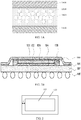
- FIG. 1B is a schematic sectional view of a semiconductor apparatus according to a first embodiment of the present invention. Using a placement direction of the semiconductor apparatus as a reference direction, a side wall of the circuit device is one surface in a vertical direction shown in FIG. 1B .
- An embodiment of the present invention provides a semiconductor apparatus.
- the semiconductor apparatus includes: a circuit device and a heat sink fin 105 that are disposed in a laminated manner, and a thermal interface material layer 104 located between the circuit device and the heat sink fin 105, where a packaging layer 120 is disposed around a side wall of the circuit device, the circuit device includes an integrated circuit die 103, the integrated circuit die 103 is provided with a pin, one surface that is of the integrated circuit die 103 and on which the pin is disposed is a mounting surface, and the side wall of the circuit device is a wall that is of the integrated circuit die 103 and that is adjacent to the mounting surface; and the thermal interface material layer 104 has a first surface facing the circuit device and the packaging layer 120 and a second surface facing the heat sink fin 105, the first surface is thermally coupled to the circuit device and the packaging layer 120, and the second surface is thermally coupled to the heat sink fin 105.
- FIG. 1B is a schematic sectional view of the semiconductor apparatus according to the first embodiment of the present invention.
- FIG. 2 is a top view of a combination of the circuit device and the packaging layer in this embodiment.
- FIG. 2 is a schematic structural diagram of the circuit device (the integrated circuit die 103) and the packaging layer 120 that are seen from top to bottom by using a placement direction of the device shown in FIG. 1B as a reference direction.
- the circuit device has a regular rectangular shape. It should be understood that, FIG. 2 shows only a positional relationship between the circuit device and the packaging layer 120.
- a shape of the circuit device is not limited to the rectangular shape in FIG. 2 , and may be any other shape. With reference to FIG.
- the packaging layer 120 provided in this embodiment is disposed around the side wall of the circuit device. That is, the packaging layer 120 may be considered as a structure that is formed by surrounding the circuit device and that envelops the side wall of the circuit device. That is, as shown in FIG. 1B , when the circuit device includes the integrated circuit die 103 and a bottom filler 101, the packaging layer 120 envelops a side wall of the integrated circuit die 103 and a side wall of the bottom filler 101.
- a top surface of the packaging layer 120 one surface that is of the packaging layer and that can be seen in FIG.
- the thermal interface material layer 104 is thermally coupled to the integrated circuit die 103 and the heat sink fin 105. In specific disposition, the thermal interface material layer 104 covers the top surfaces (surfaces shown in FIG.
- the packaging layer 120 has a particular thickness d (that is, a width of a frame-shaped surface)
- the packaging layer120 forms a frame-shaped contact surface (as shown in FIG. 2 ) that is thermally coupled to the thermal interface material layer 104.
- the packaging layer 120 has the specified thickness d to ensure that the packaging layer 120 can completely package the circuit device. Therefore, a frame of the frame-shaped contact surface has a particular width (the width is equal to the thickness of the packaging layer 120).
- a coupling area is only an area of the top surface of the integrated circuit die 103.
- the coupling area is a sum of the area of the top surface of the integrated circuit die 103 and an area of the top surface of the packaging layer 120, so that an area of a thermal coupling surface between the thermal interface material layer 104 and the integrated circuit die 103 is increased.
- the coupling area is increased, so that connection strength between the thermal interface material layer 104 and the integrated circuit die 103 is increased, and an interface stress is reduced (an entire stress stays unchanged, but a contact area is increased, so that stress impact on per unit of area is reduced), thereby improving component reliability performance.
- the packaging layer 120 is attached on the side wall of the circuit device. Therefore, during heat dissipation, heat on the side wall of the circuit device is transferred to the thermal interface material layer 104 through the packaging layer 120, and is further dissipated to the heat sink fin 105.
- a heat dissipation manner of the circuit device is dissipating heat on a top surface of the circuit device along a path from the thermal interface material layer 104 to the heat sink fin 105 and dissipating the heat on the side wall of the circuit device along a path from the packaging layer 120 through the thermal interface material layer 104 to the heat sink fin 105, so as to increase a heat dissipation area of the circuit device, thereby improving a heat dissipation effect of the circuit device.
- the packaging layer 120 uses a plastic film layer.
- the plastic film layer has a desirable packaging effect and a desirable heat transfer effect, so that the plastic film layer can rapidly transfer heat to the thermal interface material layer, thereby improving the heat dissipation effect of the circuit device.
- the entire semiconductor apparatus when a flip chip ball grid array package structure is used, the entire semiconductor apparatus includes a solder ball 108, the substrate 107, the adhesive 106, a metal bump (BUMP) 102, the circuit device (for example, the integrated circuit die 103), the packaging layer 120 (for example, the plastic film layer) disposed around the circuit device 103, the thermal interface material layer 104, and the heat sink fin 105.
- the integrated circuit die 103 is coupled to the substrate 107 by using the metal bump 102.
- the metal bump 102 is protected by the bottom filler 101, and the packaging layer 120 is disposed around the integrated circuit die 103.
- thermal coupling includes a case in which there is heat transfer between different layers, different structures, or different apparatuses.
- the thermal interface material layer 104 may be located between the integrated circuit die 103 and the heat sink fin 105.
- a substrate in the integrated circuit die 103 is thermally coupled to the thermal interface material layer 104
- the packaging layer is also thermally coupled to the thermal interface material layer 104. Heat of the integrated circuit die 103 reaches the heat sink fin 105 through the thermal interface material layer 104.
- the integrated circuit die 103, the packaging layer 120 disposed around the circuit device 103, the thermal interface material layer 104, and the heat sink fin 105 may be some or all of components of a semiconductor apparatus.
- the semiconductor apparatus may be used for the flip chip ball grid array package structure shown in the figure, but no limitation is set thereto.
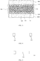
- FIG. 3 is a schematic sectional view of thermal coupling of the thermal interface material layer to the circuit device and the packaging layer according to the first embodiment.
- FIG. 3 shows only an upper half structure of the integrated circuit die 103 that are connected to the thermal interface material layer 104 being connected in FIG. 1B .
- the packaging layer 120 also only an upper half structure of the packaging layer 120 is shown.
- the upper half structure does not include the bottom filler 101.
- the thermal interface material layer 104 is thermally coupled to the integrated circuit die 103, the packaging layer 120, and the heat sink fin 105, and includes a first alloy layer 109, a nano-metal particle layer 110, and a second alloy layer 112.
- the nano-metal particle layer 110 is thermally coupled to the integrated circuit die 103 and the packaging layer 120 by using the first alloy layer 109. More specifically, as shown in FIG. 3 , the first alloy layer 109 may be located on the integrated circuit die 103 and the packaging layer 120 and under the nano-metal particle layer 110. That is, the first alloy layer 109 may be located between the integrated circuit die 103 and the nano-metal particle layer 110.
- the first alloy layer 109 increases adhesive strength between the integrated circuit die 103 and the nano-metal particle layer 110, and a coverage area of the first alloy layer 109 is increased by disposing the packaging layer 120. That is, an area of the formed first alloy layer 109 is increased, thereby increasing an area of the formed thermal interface material layer 104.
- the nano-metal particle layer 110 includes nano-metal particles and an intermediate mixture.
- the intermediate mixture includes, but is not limited to, either of the following materials: air or resin.
- the intermediate mixture is filled between multiple nano-metal particles, to make the multiple nano-metal particles form a whole.
- the nano-metal particles include, but are not limited to, silver. Diameters of the nano-metal particles are not greater than 1 micrometer. In an embodiment, the diameters of the nano-metal particles are between 50 nanometers and 200 nanometers.
- the nano-metal particle layer 110 has a relatively low thermal resistance, and forms a relatively desirable heat conduction path.
- the second alloy layer 112 is thermally coupled to the nano-metal particle layer 110 and the heat sink fin 105. More specifically, as shown in the figure, the second alloy layer 112 may be located on the nano-metal particle layer 110 and under the heat sink fin 105. That is, the second alloy layer 112 may be located between the nano-metal particle layer 110 and the heat sink fin 105. The second alloy layer 112 increases adhesive strength between the nano-metal particle layer 110 and the heat sink fin 105.
- a sintered continuous phase structure is formed at a contact portion between the first alloy layer 109 and the nano-metal particle layer 110, sintered continuous phase structures are formed at contact portions between the nano-metal particles, and a sintered continuous phase structure is formed at a contact portion between the second alloy layer 112 and the nano-metal particle layer 110.
- the sintered continuous phase structure in this specification includes, but is not limited to, a whole structure formed of metal particles as metal atoms near contact portions of the metal particles spread to metal particle interfaces and fuse with the metal particle interfaces because the metal particles are sintered.
- FIG. 4 is a schematic sectional view of a first embodiment of the first alloy layer 109 in FIG. 3.
- FIG. 4 also shows only an upper half structure of the packaging layer 120 and the integrated circuit die 103.
- the first alloy layer 109 includes a first adhesive layer 114 and a first co-sintered layer 115.
- a co-sintered layer in this specification includes, but is not limited to, a metal layer that is generated in a packaging process and that fuses with a thermal interface material layer, and the metal layer and particles in the thermal interface material layer are co-sintered to form a heat flux path.
- the first adhesive layer 114 is thermally coupled to the integrated circuit die 103 and the packaging layer 120.
- the first co-sintered layer 115 is thermally coupled to the nano-metal particle layer 110.
- a sintered continuous phase structure is formed at a contact portion between the first co-sintered layer 115 and the nano-metal particle layer 110.
- the first adhesive layer 114 may be located on the integrated circuit die 103 and the packaging layer 120, and the first co-sintered layer 115 may be located on the first adhesive layer 114 and under the nano-metal particle layer 110.
- the first adhesive layer 114 includes, but is not limited to, any one of the following materials: titanium, chromium, nickel, or nickel/vanadium.
- the first adhesive layer 114 increases bonding strength between the integrated circuit die 103 and the first co-sintered layer 115.
- the first co-sintered layer 115 includes, but is not limited to, any one of the following materials: silver, gold, or copper.
- FIG. 5 is a schematic sectional view of a second embodiment of the first alloy layer 109 in FIG. 3.
- FIG. 5 also shows only an upper half structure of the packaging layer 120 and the integrated circuit die 103.
- the first alloy layer 109 in FIG. 4 further includes a first buffer layer 116 located between the first adhesive layer 114 and the first co-sintered layer 115.
- the first buffer layer 116 includes, but is not limited to, any one of the following materials: aluminum, copper, or nickel.
- the first buffer layer 116 provides a stress buffering function during deformation caused by heat processing, and reduces a risk of a crack that appears between the integrated circuit die 103 and the thermal interface material layer 114 or in the middle of the thermal interface material layer 114, thereby increasing reliability of the semiconductor apparatus.
- FIG. 6 is a schematic sectional view of a first embodiment of the second alloy layer 112 in FIG. 3 .
- the second alloy layer 112 includes a second co-sintered layer 118 and a second adhesive layer 117.
- the second co-sintered layer 118 is thermally coupled to the nano-metal particle layer 110.
- a sintered continuous phase structure is formed at a contact portion between the second co-sintered layer 118 and the nano-metal particle layer 110.
- the second adhesive layer 117 is thermally coupled to the heat sink fin 105.
- the second co-sintered layer 118 may be located on the nano-metal particle layer 110, and the second adhesive layer 117 may be located on the second co-sintered layer 118 and under the heat sink fin 105.
- the second co-sintered layer 118 includes, but is not limited to, any one of the following materials: silver, gold, or copper.
- the second adhesive layer 117 includes, but is not limited to, any one of the following materials: titanium, chromium, nickel, or nickel/vanadium. The second adhesive layer 117 increases bonding strength between the second co-sintered layer 115 and the heat sink fin 105.
- FIG. 7 is a schematic sectional view of a second embodiment of the second alloy layer 112 in FIG. 3 .
- the second alloy layer 112 in FIG. 7 further includes a second buffer layer 119 located between the second adhesive layer 117 and the second co-sintered layer 118.
- the second buffer layer 119 includes, but is not limited to, any one of the following materials: aluminum, copper, nickel, or nickel/vanadium.
- the second buffer layer 119 provides a buffering function during deformation caused by heat processing, and reduces a risk of a crack that appears between the thermal interface material layer and the heat sink fin 105 or in the middle of the thermal interface material layer 114, thereby increasing reliability of the apparatus.
- the thermal interface material layer in this embodiment of the present invention no longer includes high polymer materials with a relatively low thermal conductivity in silver adhesive materials, but includes nano-metal particles instead.
- the thermal interface material in this embodiment of the present invention has a relatively high thermal conductivity, so as to greatly improve thermal conductivity effectiveness of an entire heat conduction path, thereby better meeting a heat dissipation requirement of a high-power chip.
- one packaging layer 120 is disposed around an exterior side of the integrated circuit die 103, so as to increase a laying area of the thermal interface material layer, increase an area of a contact surface of the thermal interface material layer, reduce an interface stress, and correspondingly improve component reliability.
- FIG. 8 is a flowchart 700 of a semiconductor apparatus manufacturing method according to a second embodiment of the present invention.
- a packaging layer is disposed around a side wall of a circuit device.
- the circuit device includes an integrated circuit die.
- the integrated circuit die is provided with a pin, and one surface that is of the integrated circuit die and on which the pin is disposed is a mounting surface.
- the side wall of the circuit device is a wall that is of the integrated circuit die and that is adjacent to the mounting surface.
- a thermal interface material layer is generated.
- the thermal interface material layer has a first surface facing the circuit device and the packaging layer and a second surface facing the heat sink fin.
- the first surface is thermally coupled to the circuit device and the packaging layer, and the second surface is thermally coupled to the heat sink fin.
- the disposing a packaging layer around a side wall of a circuit device includes: disposing the packaging layer around the side wall by using a plastic film as a material for manufacturing the packaging layer.
- the plastic film layer has a desirable heat transfer effect, and can rapidly transfer heat generated on the side wall of the circuit device to the thermal interface material layer, thereby improving heat dissipation efficiency of the circuit device.
- the thermal interface material layer has the first surface facing the circuit device and the packaging layer and the second surface facing the heat sink fin. Specifically:
- a first alloy layer is generated.
- a nano-metal particle layer is generated by using nano-metal particles that are coupled to each other and an intermediate mixture. Diameters of the nano-metal particles are not greater than 1 micrometer. For example, the diameters of the nano-metal particles are between 50 nanometers and 200 nanometers.
- the intermediate mixture includes, but is not limited to, either of the following materials: air or resin. In an embodiment, the nano-metal particles include, but are not limited to, silver.
- a second alloy layer is generated. The nano-metal particle layer is thermally coupled to the circuit device and the packaging layer by using the first alloy layer. The second alloy layer is thermally coupled to the nano-metal particle layer and the heat sink fin.
- the method further includes: forming a sintered continuous phase structure at a contact portion between the first alloy layer and the nano-metal particle layer, forming sintered continuous phase structures at contact portions between the nano-metal particles, and forming a sintered continuous phase structure at a contact portion between the second alloy layer and the nano-metal particle layer.
- the method may be used for a flip chip ball grid array package structure, but no limitation is set thereto.
- the generating a first alloy layer includes: generating a first adhesive layer and a first co-sintered layer, thermally coupling the first adhesive layer to the circuit device and the packaging layer, coupling the first co-sintered layer to the nano-metal particle layer, and forming a sintered continuous phase structure at a contact portion between the first co-sintered layer and the nano-metal particle layer.
- the first adhesive layer includes, but is not limited to, any one of the following materials: titanium, chromium, nickel, or nickel/vanadium.
- the first co-sintered layer includes, but is not limited to, any one of the following materials: silver, gold, or copper.
- the generating a first alloy layer further includes: generating a first buffer layer between the first adhesive layer and the first co-sintered layer.
- the first buffer layer includes, but is not limited to, any one of the following materials: aluminum, copper, nickel, or nickel/vanadium.
- the generating a second alloy layer includes: generating a second adhesive layer and a second co-sintered layer, thermally coupling the second adhesive layer to the heat sink fin, thermally coupling the second co-sintered layer to the nano-metal particle layer, and forming a sintered continuous phase structure at a contact portion between the second co-sintered layer and the nano-metal particle layer.
- the second adhesive layer includes, but is not limited to, any one of the following materials: titanium, chromium, nickel, or nickel/vanadium.
- the second co-sintered layer includes, but is not limited to, any one of the following materials: silver, gold, or copper.
- the generating a second alloy layer further includes: generating a second buffer layer between the second adhesive layer and the second co-sintered layer.
- the second buffer layer includes, but is not limited to, any one of the following materials: aluminum, copper, nickel, or nickel/vanadium.
- the circuit device may include the integrated circuit die.
- Thermally coupling the first alloy layer to the circuit device and the packaging layer includes thermally coupling the first alloy layer to a substrate in the integrated circuit die and the packaging layer.
Landscapes
- Chemical & Material Sciences (AREA)
- Engineering & Computer Science (AREA)
- Nanotechnology (AREA)
- Physics & Mathematics (AREA)
- Composite Materials (AREA)
- Condensed Matter Physics & Semiconductors (AREA)
- General Physics & Mathematics (AREA)
- Materials Engineering (AREA)
- Crystallography & Structural Chemistry (AREA)
- Cooling Or The Like Of Semiconductors Or Solid State Devices (AREA)
- Ceramic Engineering (AREA)
Description
- The present invention relates to the field of semiconductor technologies, and in particular, to a semiconductor apparatus and a manufacturing method thereof.
-
FIG. 1A is a schematic sectional view of an integrated circuit chip in the prior art and a partial package structure of the integrated circuit chip. The structure includes an integrated circuit chip 1A02, a thermal interface material layer 1A04, and a heat sink 1A06. The thermal interface material layer 1A04 has multiple metal particles 1A08 distributed in a form of a dispersed phase. Heat generated by the integrated circuit chip 1A02 in an operating process is guided into the heat sink 1A06 through the thermal interface material layer 1A04 on a rear side of the chip. However, in the prior art, because a size of the integrated circuit chip 1A02 is limited, a heat transfer effect is relatively undesirable. Consequently, it is very difficult to meet a heat dissipation requirement of a high-power chip. - A US patent application, numbered as
US20090294938 , provides a filp-chip package with fan-out WLCSP. - A US patent application, numbered as
US20140131856 , provides a semiconductor device and manufacture method thereof. - A US patent application, numbered as
US20120119346 , provides a semiconductor package and method of forming the same. - A Chinese patent application, numbered as
CN105355610 , provides a circuit device and manufacture method thereof. - A US patent application, numbered as
US20080073776 , provides a sintered metallic thermal interface materials for microelectronic cooling assembles. - Embodiments of the present invention provide a semiconductor apparatus and a manufacturing method thereof. In the semiconductor apparatus, a contact area between a thermal interface material layer and a circuit device is increased by using a disposed packaging layer, so as to greatly improve thermal conductivity effectiveness of an entire heat conduction path, thereby better meeting a heat dissipation requirement of a high-power-consumption circuit device.
- According to a first aspect, an embodiment of the present invention provides a semiconductor apparatus, including a circuit device and a heat sink fin that are disposed in a laminated manner, and a thermal interface material layer located between the circuit device and the heat sink fin, where
a packaging layer is disposed around a side wall of the circuit device, the circuit device includes an integrated circuit die, the integrated circuit die is provided with a pin, one surface that is of the integrated circuit die and on which the pin is disposed is a mounting surface, and the side wall of the circuit device is a wall that is of the integrated circuit die and that is adjacent to the mounting surface; and
the thermal interface material layer has a first surface facing the circuit device and the packaging layer and a second surface facing the heat sink fin, the first surface is thermally coupled to the circuit device and the packaging layer, and the second surface is thermally coupled to the heat sink fin,
the semiconductor device further comprises a substrate, the integrated circuit die is coupled to the substrate by using a metal bump, the metal bump is protected by bottom filler, the packaging layer envelops the side wall of the integrated circuit die and a side wall of the bottom filler,
the heat sink fin is fastened on the substrate by using an adhesive. - In the foregoing solution, because the packaging layer is disposed around the circuit device, and the packaging layer and the circuit device are both thermally coupled to the thermal interface material layer, a contact area between the circuit device and the thermal interface material layer is increased. In addition, heat generated on the side wall of the circuit device may be transferred to the thermal interface material layer through the packaging layer, and then transferred to the heat sink fin, thereby improving a heat dissipation effect of the semiconductor apparatus. In addition, one packaging layer is disposed around an exterior side of the circuit device, so as to increase a laying area of the thermal interface material layer, increase an area of a contact surface of the thermal interface material layer, reduce an interface stress, and correspondingly improve component reliability.
- The packaging layer uses a plastic film layer. The plastic film layer has a desirable heat transfer effect, and can rapidly transfer the heat generated on the side wall of the circuit device to the thermal interface material layer, thereby improving heat dissipation efficiency of the circuit device.
- The thermal interface material layer includes: a first alloy layer, thermally coupled to the circuit device and the packaging layer; a nano-metal particle layer, thermally coupled to the first alloy layer, where the nano-metal particle layer includes multiple nano-metal particles that are coupled to each other and an intermediate mixture, and the intermediate mixture is filled between the multiple nano-metal particles; and a second alloy layer, thermally coupled to the nano-metal particle layer and the heat sink fin. The used thermal interface material layer no longer includes high polymer materials with a relatively low thermal conductivity in silver adhesive materials, but includes nano-metal particles instead. The thermal interface material in this embodiment of the present invention has a relatively high thermal conductivity, so as to greatly improve thermal conductivity effectiveness of an entire heat conduction path, thereby better meeting a heat dissipation requirement of a high-power chip.
- In specific disposition, a sintered continuous phase structure is formed at a contact portion between the first alloy layer and the nano-metal particle layer, sintered continuous phase structure is formed at a contact portion between the second alloy layer and the nano-metal particle layer. A connection effect between the circuit device and the heat sink fin is improved by using the sintered continuous phase structure, and a heat transfer effect between the circuit device and the heat sink fin is improved.
- In a specific implementation solution, the nano-metal particles include silver, and have a desirable heat transfer effect. In addition, in specific disposition, diameters of the nano-metal particles are between 50 nanometers and 200 nanometers.
- The semiconductor apparatus provided in this embodiment is used for a flip chip ball grid array package structure.
- The first alloy layer includes a first adhesive layer and a first co-sintered layer, the first adhesive layer is thermally coupled to the circuit device and the packaging layer, the first co-sintered layer is coupled to the nano-metal particle layer, and a sintered continuous phase structure is formed at a contact portion between the first co-sintered layer and the nano-metal particle layer. By using the foregoing structure, connection strength of thermal coupling of the first alloy layer to the circuit device and the packaging layer is increased, and a desirable heat transfer effect is achieved.
- In specific disposition, the first adhesive layer includes any one of the following materials: titanium, chromium, nickel, or a nickel-vanadium alloy, and the first co-sintered layer includes any one of the following materials: silver, gold, or copper. The foregoing materials all have relatively desirable heat transfer effects.
- In addition, in a solution, the first alloy layer further includes a first buffer layer, located between the first adhesive layer and the first co-sintered layer, and the first buffer layer includes any one of the following materials: aluminum, copper, nickel, or a nickel-vanadium alloy.
- In specific disposition, the second alloy layer includes a second adhesive layer and a second co-sintered layer, the second adhesive layer is thermally coupled to the heat sink fin, the second co-sintered layer is thermally coupled to the nano-metal particle layer, and a sintered continuous phase structure is formed at a contact portion between the second co-sintered layer and the nano-metal particle layer. By using the foregoing structure, connection strength of thermal coupling of the second alloy layer to the heat sink fin is increased, and a desirable heat transfer effect is achieved.
- In addition, in specific disposition, the second adhesive layer includes any one of the following materials: titanium, chromium, nickel, or a nickel-vanadium alloy, and the second co-sintered layer includes any one of the following materials: silver, gold, or copper. The foregoing materials all have relatively desirable heat transfer effects.
- In a solution, the second alloy layer further includes a second buffer layer, located between the second adhesive layer and the second co-sintered layer, and the second buffer layer includes any one of the following materials: aluminum, copper, nickel, or a nickel-vanadium alloy.
- Diameters of the nano-metal particles are not greater than 1 micrometer.
- Different materials may be selected for the intermediate mixture. In a specific implementation, the intermediate mixture includes either of the following materials: air or resin.
- An embodiment of the present invention provides a semiconductor apparatus manufacturing method, including: disposing a packaging layer around a side wall of a circuit device, where the circuit device includes an integrated circuit die, the integrated circuit die is provided with a pin, one surface that is of the integrated circuit die and on which the pin is disposed is a mounting surface, and the side wall of the circuit device is a wall that is of the integrated circuit die and that is adjacent to the mounting surface;
generating a thermal interface material layer, where the thermal interface material layer has a first surface facing the circuit device and the packaging layer and a second surface facing the heat sink fin; and
thermally coupling the first surface to the circuit device and the packaging layer, and thermally coupling the second surface to the heat sink fin. - In the foregoing solution, because the packaging layer is disposed around the circuit device, and the packaging layer and the circuit device are both thermally coupled to the thermal interface material layer, a contact area between the circuit device and the thermal interface material layer is increased. In addition, heat generated on the side wall of the circuit device may be transferred to the thermal interface material layer through the packaging layer, and then transferred to the heat sink fin, thereby improving a heat dissipation effect of the semiconductor apparatus. In addition, one packaging layer is disposed around an exterior side of the circuit device, so as to increase a laying area of the thermal interface material layer, increase an area of a contact surface of the thermal interface material layer, reduce an interface stress, and correspondingly improve component reliability.
- During specific fabrication, the generating a thermal interface material layer, where the thermal interface material layer has a first surface facing the circuit device and the packaging layer and a second surface facing the heat sink fin is specifically:
- generating a first alloy layer;
- generating a nano-metal particle layer by using multiple nano-metal particles that are coupled to each other and an intermediate mixture, and filling the intermediate mixture between the multiple nano-metal particles;
- generating a second alloy layer; and
- thermally coupling the nano-metal particle layer to the first alloy layer and the second alloy layer separately, where one surface that is of the first alloy layer and that deviates from the nano-metal particle layer is the first surface, and one surface that is of the second alloy layer and that deviates from the nano-metal particle layer is the second surface.
- The manufacturing method further includes: forming a sintered continuous phase structure at a contact portion between the first alloy layer and the nano-metal particle layer, forming sintered continuous phase structures at contact portions between the nano-metal particles, and forming a sintered continuous phase structure at a contact portion between the second alloy layer and the nano-metal particle layer.
- Diameters of the nano-metal particles are not greater than 1 micrometer.
- The intermediate mixture includes either of the following materials: air or resin.
- During specific fabrication of the first alloy layer, a first adhesive layer and a first co-sintered layer are generated, the first adhesive layer is thermally coupled to the circuit device and the packaging layer, the first co-sintered layer is coupled to the nano-metal particle layer, and a sintered continuous phase structure is formed at a contact portion between the first co-sintered layer and the nano-metal particle layer.
- During specific fabrication of the second alloy layer, a second adhesive layer and a second co-sintered layer are generated, the second adhesive layer is thermally coupled to the heat sink fin, the second co-sintered layer is thermally coupled to the nano-metal particle layer, and a sintered continuous phase structure is formed at a contact portion between the second co-sintered layer and the nano-metal particle layer.
- The disposing a packaging layer around a side wall of a circuit device includes: disposing the packaging layer around the side wall by using a plastic film as a material for manufacturing the packaging layer. The plastic film has a desirable heat transfer effect. Heat dissipation efficiency of the circuit device is improved by using the disposed packaging layer that is fabricated from the plastic film.
- To describe the technical solutions in the embodiments of the present invention or in the prior art more clearly, the following briefly describes the accompanying drawings required for describing the embodiments or the prior art. Apparently, the accompanying drawings in the following description show merely some embodiments of the present invention, and a person of ordinary skill in the art may still derive other drawings from these accompanying drawings without creative efforts.
-
FIG. 1A is a schematic sectional view of a package structure including a semiconductor apparatus in the prior art; -
FIG. 1B is a schematic sectional view of a semiconductor apparatus according to a first embodiment of the present invention; -
FIG. 2 is a schematic diagram of a combination of a circuit device and a packaging layer of the semiconductor apparatus according to the first embodiment of the present invention; -
FIG. 3 is a schematic sectional view of thermal coupling of a thermal interface material layer to the circuit device and the packaging layer according to the first embodiment; -
FIG. 4 is a schematic sectional view of a first embodiment of a first alloy layer inFIG. 3 ; -
FIG. 5 is a schematic sectional view of a second embodiment of the first alloy layer inFIG. 3 ; -
FIG. 6 is a schematic sectional view of a first embodiment of a second alloy layer inFIG. 3 ; -
FIG. 7 is a schematic sectional view of a second embodiment of the second alloy layer inFIG. 3 ; and -
FIG. 8 is a flowchart of a semiconductor apparatus manufacturing method according to a second embodiment of the present invention. - The following clearly and completely describes the technical solutions in the embodiments of the present invention with reference to the accompanying drawings in the embodiments of the present invention. Apparently, the described embodiments are merely some but not all of the embodiments of the present invention. All other embodiments obtained by a person of ordinary skill in the art based on the embodiments of the present invention without creative efforts shall fall within the protection scope of the present invention.
- For convenience of description, a side wall of a circuit device is defined in the embodiments. In the embodiments, the side wall of the circuit device is a wall that is of the circuit device and that is adjacent to one surface (a mounting surface) on which a pin is disposed. In
FIG. 1B, FIG. 1B is a schematic sectional view of a semiconductor apparatus according to a first embodiment of the present invention. Using a placement direction of the semiconductor apparatus as a reference direction, a side wall of the circuit device is one surface in a vertical direction shown inFIG. 1B . - An embodiment of the present invention provides a semiconductor apparatus. The semiconductor apparatus includes: a circuit device and a
heat sink fin 105 that are disposed in a laminated manner, and a thermalinterface material layer 104 located between the circuit device and theheat sink fin 105, where
apackaging layer 120 is disposed around a side wall of the circuit device, the circuit device includes an integrated circuit die 103, the integrated circuit die 103 is provided with a pin, one surface that is of the integrated circuit die 103 and on which the pin is disposed is a mounting surface, and the side wall of the circuit device is a wall that is of the integrated circuit die 103 and that is adjacent to the mounting surface; and
the thermalinterface material layer 104 has a first surface facing the circuit device and thepackaging layer 120 and a second surface facing theheat sink fin 105, the first surface is thermally coupled to the circuit device and thepackaging layer 120, and the second surface is thermally coupled to theheat sink fin 105. - Referring to
FIG. 1B and FIG. 2 together,FIG. 1B is a schematic sectional view of the semiconductor apparatus according to the first embodiment of the present invention.FIG. 2 is a top view of a combination of the circuit device and the packaging layer in this embodiment.FIG. 2 is a schematic structural diagram of the circuit device (the integrated circuit die 103) and thepackaging layer 120 that are seen from top to bottom by using a placement direction of the device shown inFIG. 1B as a reference direction. InFIG. 2 , the circuit device has a regular rectangular shape. It should be understood that,FIG. 2 shows only a positional relationship between the circuit device and thepackaging layer 120. A shape of the circuit device is not limited to the rectangular shape inFIG. 2 , and may be any other shape. With reference toFIG. 1B and FIG. 2 , it may be known that, thepackaging layer 120 provided in this embodiment is disposed around the side wall of the circuit device. That is, thepackaging layer 120 may be considered as a structure that is formed by surrounding the circuit device and that envelops the side wall of the circuit device. That is, as shown inFIG. 1B , when the circuit device includes the integrated circuit die 103 and abottom filler 101, thepackaging layer 120 envelops a side wall of the integrated circuit die 103 and a side wall of thebottom filler 101. In addition, a top surface of the packaging layer 120 (one surface that is of the packaging layer and that can be seen inFIG. 2 ) is flush with a top surface of the integrated circuit die 103 (one surface that is of the integrated circuit die 103 and that can be seen inFIG. 2 ). The top surface of thepackaging layer 120 and the top surface of the integrated circuit die 103 together form a contact surface that is connected to the thermalinterface material layer 104. Theheat sink fin 105 is fastened on asubstrate 107 by using an adhesive 106, and the pin of the integrated circuit die 103 is connected to a circuit of thesubstrate 107. The thermalinterface material layer 104 is thermally coupled to the integrated circuit die 103 and theheat sink fin 105. In specific disposition, the thermalinterface material layer 104 covers the top surfaces (surfaces shown inFIG. 2 ) of the integrated circuit die 103 and thepackaging layer 120, and is thermally coupled to the top surfaces. Because thepackaging layer 120 has a particular thickness d (that is, a width of a frame-shaped surface), the packaging layer120 forms a frame-shaped contact surface (as shown inFIG. 2 ) that is thermally coupled to the thermalinterface material layer 104. In addition, in specific disposition, thepackaging layer 120 has the specified thickness d to ensure that thepackaging layer 120 can completely package the circuit device. Therefore, a frame of the frame-shaped contact surface has a particular width (the width is equal to the thickness of the packaging layer 120). Specifically, when there is nopackaging layer 120, a coupling area is only an area of the top surface of the integrated circuit die 103. After thepackaging layer 120 is added, as shown inFIG. 2 , the coupling area is a sum of the area of the top surface of the integrated circuit die 103 and an area of the top surface of thepackaging layer 120, so that an area of a thermal coupling surface between the thermalinterface material layer 104 and the integrated circuit die 103 is increased. In addition, the coupling area is increased, so that connection strength between the thermalinterface material layer 104 and the integrated circuit die 103 is increased, and an interface stress is reduced (an entire stress stays unchanged, but a contact area is increased, so that stress impact on per unit of area is reduced), thereby improving component reliability performance. - In addition, in specific disposition, the
packaging layer 120 is attached on the side wall of the circuit device. Therefore, during heat dissipation, heat on the side wall of the circuit device is transferred to the thermalinterface material layer 104 through thepackaging layer 120, and is further dissipated to theheat sink fin 105. By using the foregoing structure, it may be known that a heat dissipation manner of the circuit device is dissipating heat on a top surface of the circuit device along a path from the thermalinterface material layer 104 to theheat sink fin 105 and dissipating the heat on the side wall of the circuit device along a path from thepackaging layer 120 through the thermalinterface material layer 104 to theheat sink fin 105, so as to increase a heat dissipation area of the circuit device, thereby improving a heat dissipation effect of the circuit device. - In a specific implementation, the
packaging layer 120 uses a plastic film layer. The plastic film layer has a desirable packaging effect and a desirable heat transfer effect, so that the plastic film layer can rapidly transfer heat to the thermal interface material layer, thereby improving the heat dissipation effect of the circuit device. - As shown in
FIG. 1B and FIG. 2 , when a flip chip ball grid array package structure is used, the entire semiconductor apparatus includes asolder ball 108, thesubstrate 107, the adhesive 106, a metal bump (BUMP) 102, the circuit device (for example, the integrated circuit die 103), the packaging layer 120 (for example, the plastic film layer) disposed around thecircuit device 103, the thermalinterface material layer 104, and theheat sink fin 105. The integrated circuit die 103 is coupled to thesubstrate 107 by using themetal bump 102. Themetal bump 102 is protected by thebottom filler 101, and thepackaging layer 120 is disposed around the integrated circuit die 103. In addition, in specific disposition, in this embodiment, thermal coupling includes a case in which there is heat transfer between different layers, different structures, or different apparatuses. More specifically, the thermalinterface material layer 104 may be located between the integrated circuit die 103 and theheat sink fin 105. In addition, a substrate in the integrated circuit die 103 is thermally coupled to the thermalinterface material layer 104, and the packaging layer is also thermally coupled to the thermalinterface material layer 104. Heat of the integrated circuit die 103 reaches theheat sink fin 105 through the thermalinterface material layer 104. - The integrated circuit die 103, the
packaging layer 120 disposed around thecircuit device 103, the thermalinterface material layer 104, and theheat sink fin 105 may be some or all of components of a semiconductor apparatus. The semiconductor apparatus may be used for the flip chip ball grid array package structure shown in the figure, but no limitation is set thereto. -
FIG. 3 is a schematic sectional view of thermal coupling of the thermal interface material layer to the circuit device and the packaging layer according to the first embodiment.FIG. 3 shows only an upper half structure of the integrated circuit die 103 that are connected to the thermalinterface material layer 104 being connected inFIG. 1B . For thepackaging layer 120, also only an upper half structure of thepackaging layer 120 is shown. The upper half structure does not include thebottom filler 101. The thermalinterface material layer 104 is thermally coupled to the integrated circuit die 103, thepackaging layer 120, and theheat sink fin 105, and includes afirst alloy layer 109, a nano-metal particle layer 110, and asecond alloy layer 112. - The nano-
metal particle layer 110 is thermally coupled to the integrated circuit die 103 and thepackaging layer 120 by using thefirst alloy layer 109. More specifically, as shown inFIG. 3 , thefirst alloy layer 109 may be located on the integrated circuit die 103 and thepackaging layer 120 and under the nano-metal particle layer 110. That is, thefirst alloy layer 109 may be located between the integrated circuit die 103 and the nano-metal particle layer 110. Thefirst alloy layer 109 increases adhesive strength between the integrated circuit die 103 and the nano-metal particle layer 110, and a coverage area of thefirst alloy layer 109 is increased by disposing thepackaging layer 120. That is, an area of the formedfirst alloy layer 109 is increased, thereby increasing an area of the formed thermalinterface material layer 104. - The nano-
metal particle layer 110 includes nano-metal particles and an intermediate mixture. The intermediate mixture includes, but is not limited to, either of the following materials: air or resin. The intermediate mixture is filled between multiple nano-metal particles, to make the multiple nano-metal particles form a whole. The nano-metal particles include, but are not limited to, silver. Diameters of the nano-metal particles are not greater than 1 micrometer. In an embodiment, the diameters of the nano-metal particles are between 50 nanometers and 200 nanometers. The nano-metal particle layer 110 has a relatively low thermal resistance, and forms a relatively desirable heat conduction path. - The
second alloy layer 112 is thermally coupled to the nano-metal particle layer 110 and theheat sink fin 105. More specifically, as shown in the figure, thesecond alloy layer 112 may be located on the nano-metal particle layer 110 and under theheat sink fin 105. That is, thesecond alloy layer 112 may be located between the nano-metal particle layer 110 and theheat sink fin 105. Thesecond alloy layer 112 increases adhesive strength between the nano-metal particle layer 110 and theheat sink fin 105. - In an embodiment, a sintered continuous phase structure is formed at a contact portion between the
first alloy layer 109 and the nano-metal particle layer 110, sintered continuous phase structures are formed at contact portions between the nano-metal particles, and a sintered continuous phase structure is formed at a contact portion between thesecond alloy layer 112 and the nano-metal particle layer 110. The sintered continuous phase structure in this specification includes, but is not limited to, a whole structure formed of metal particles as metal atoms near contact portions of the metal particles spread to metal particle interfaces and fuse with the metal particle interfaces because the metal particles are sintered. -
FIG. 4 is a schematic sectional view of a first embodiment of thefirst alloy layer 109 inFIG. 3. FIG. 4 also shows only an upper half structure of thepackaging layer 120 and the integrated circuit die 103. As shown in the figure, thefirst alloy layer 109 includes a first adhesive layer 114 and a first co-sintered layer 115. A co-sintered layer in this specification includes, but is not limited to, a metal layer that is generated in a packaging process and that fuses with a thermal interface material layer, and the metal layer and particles in the thermal interface material layer are co-sintered to form a heat flux path. The first adhesive layer 114 is thermally coupled to the integrated circuit die 103 and thepackaging layer 120. The first co-sintered layer 115 is thermally coupled to the nano-metal particle layer 110. A sintered continuous phase structure is formed at a contact portion between the first co-sintered layer 115 and the nano-metal particle layer 110. Specifically, the first adhesive layer 114 may be located on the integrated circuit die 103 and thepackaging layer 120, and the first co-sintered layer 115 may be located on the first adhesive layer 114 and under the nano-metal particle layer 110. The first adhesive layer 114 includes, but is not limited to, any one of the following materials: titanium, chromium, nickel, or nickel/vanadium. The first adhesive layer 114 increases bonding strength between the integrated circuit die 103 and the first co-sintered layer 115. The first co-sintered layer 115 includes, but is not limited to, any one of the following materials: silver, gold, or copper. -
FIG. 5 is a schematic sectional view of a second embodiment of thefirst alloy layer 109 inFIG. 3. FIG. 5 also shows only an upper half structure of thepackaging layer 120 and the integrated circuit die 103. Compared withFIG. 3 , thefirst alloy layer 109 inFIG. 4 further includes a first buffer layer 116 located between the first adhesive layer 114 and the first co-sintered layer 115. The first buffer layer 116 includes, but is not limited to, any one of the following materials: aluminum, copper, or nickel. The first buffer layer 116 provides a stress buffering function during deformation caused by heat processing, and reduces a risk of a crack that appears between the integrated circuit die 103 and the thermal interface material layer 114 or in the middle of the thermal interface material layer 114, thereby increasing reliability of the semiconductor apparatus. -
FIG. 6 is a schematic sectional view of a first embodiment of thesecond alloy layer 112 inFIG. 3 . As shown in the figure, thesecond alloy layer 112 includes a secondco-sintered layer 118 and a secondadhesive layer 117. The secondco-sintered layer 118 is thermally coupled to the nano-metal particle layer 110. A sintered continuous phase structure is formed at a contact portion between the secondco-sintered layer 118 and the nano-metal particle layer 110. The secondadhesive layer 117 is thermally coupled to theheat sink fin 105. Specifically, the secondco-sintered layer 118 may be located on the nano-metal particle layer 110, and the secondadhesive layer 117 may be located on the secondco-sintered layer 118 and under theheat sink fin 105. The secondco-sintered layer 118 includes, but is not limited to, any one of the following materials: silver, gold, or copper. The secondadhesive layer 117 includes, but is not limited to, any one of the following materials: titanium, chromium, nickel, or nickel/vanadium. The secondadhesive layer 117 increases bonding strength between the second co-sintered layer 115 and theheat sink fin 105. -
FIG. 7 is a schematic sectional view of a second embodiment of thesecond alloy layer 112 inFIG. 3 . Compared withFIG. 6 , thesecond alloy layer 112 inFIG. 7 further includes asecond buffer layer 119 located between the secondadhesive layer 117 and the secondco-sintered layer 118. Thesecond buffer layer 119 includes, but is not limited to, any one of the following materials: aluminum, copper, nickel, or nickel/vanadium. Thesecond buffer layer 119 provides a buffering function during deformation caused by heat processing, and reduces a risk of a crack that appears between the thermal interface material layer and theheat sink fin 105 or in the middle of the thermal interface material layer 114, thereby increasing reliability of the apparatus. - In conclusion, because the thermal interface material layer in this embodiment of the present invention no longer includes high polymer materials with a relatively low thermal conductivity in silver adhesive materials, but includes nano-metal particles instead. The thermal interface material in this embodiment of the present invention has a relatively high thermal conductivity, so as to greatly improve thermal conductivity effectiveness of an entire heat conduction path, thereby better meeting a heat dissipation requirement of a high-power chip. In addition, one
packaging layer 120 is disposed around an exterior side of the integrated circuit die 103, so as to increase a laying area of the thermal interface material layer, increase an area of a contact surface of the thermal interface material layer, reduce an interface stress, and correspondingly improve component reliability. -
FIG. 8 is aflowchart 700 of a semiconductor apparatus manufacturing method according to a second embodiment of the present invention. As shown in the figure, instep 702, a packaging layer is disposed around a side wall of a circuit device. The circuit device includes an integrated circuit die. The integrated circuit die is provided with a pin, and one surface that is of the integrated circuit die and on which the pin is disposed is a mounting surface. The side wall of the circuit device is a wall that is of the integrated circuit die and that is adjacent to the mounting surface. Instep 704, a thermal interface material layer is generated. The thermal interface material layer has a first surface facing the circuit device and the packaging layer and a second surface facing the heat sink fin. Instep 706, the first surface is thermally coupled to the circuit device and the packaging layer, and the second surface is thermally coupled to the heat sink fin. - In addition, the disposing a packaging layer around a side wall of a circuit device includes: disposing the packaging layer around the side wall by using a plastic film as a material for manufacturing the packaging layer. The plastic film layer has a desirable heat transfer effect, and can rapidly transfer heat generated on the side wall of the circuit device to the thermal interface material layer, thereby improving heat dissipation efficiency of the circuit device.
- During specific manufacturing, the thermal interface material layer is generated. The thermal interface material layer has the first surface facing the circuit device and the packaging layer and the second surface facing the heat sink fin. Specifically:
- A first alloy layer is generated. A nano-metal particle layer is generated by using nano-metal particles that are coupled to each other and an intermediate mixture. Diameters of the nano-metal particles are not greater than 1 micrometer. For example, the diameters of the nano-metal particles are between 50 nanometers and 200 nanometers. The intermediate mixture includes, but is not limited to, either of the following materials: air or resin. In an embodiment, the nano-metal particles include, but are not limited to, silver. A second alloy layer is generated. The nano-metal particle layer is thermally coupled to the circuit device and the packaging layer by using the first alloy layer. The second alloy layer is thermally coupled to the nano-metal particle layer and the heat sink fin.
- In an embodiment, the method further includes: forming a sintered continuous phase structure at a contact portion between the first alloy layer and the nano-metal particle layer, forming sintered continuous phase structures at contact portions between the nano-metal particles, and forming a sintered continuous phase structure at a contact portion between the second alloy layer and the nano-metal particle layer.
- In an embodiment, the method may be used for a flip chip ball grid array package structure, but no limitation is set thereto.
- In an embodiment, the generating a first alloy layer includes: generating a first adhesive layer and a first co-sintered layer, thermally coupling the first adhesive layer to the circuit device and the packaging layer, coupling the first co-sintered layer to the nano-metal particle layer, and forming a sintered continuous phase structure at a contact portion between the first co-sintered layer and the nano-metal particle layer. The first adhesive layer includes, but is not limited to, any one of the following materials: titanium, chromium, nickel, or nickel/vanadium. The first co-sintered layer includes, but is not limited to, any one of the following materials: silver, gold, or copper. In another embodiment, the generating a first alloy layer further includes: generating a first buffer layer between the first adhesive layer and the first co-sintered layer. The first buffer layer includes, but is not limited to, any one of the following materials: aluminum, copper, nickel, or nickel/vanadium.
- In an embodiment, the generating a second alloy layer includes: generating a second adhesive layer and a second co-sintered layer, thermally coupling the second adhesive layer to the heat sink fin, thermally coupling the second co-sintered layer to the nano-metal particle layer, and forming a sintered continuous phase structure at a contact portion between the second co-sintered layer and the nano-metal particle layer. The second adhesive layer includes, but is not limited to, any one of the following materials: titanium, chromium, nickel, or nickel/vanadium. The second co-sintered layer includes, but is not limited to, any one of the following materials: silver, gold, or copper. In another embodiment, the generating a second alloy layer further includes: generating a second buffer layer between the second adhesive layer and the second co-sintered layer. The second buffer layer includes, but is not limited to, any one of the following materials: aluminum, copper, nickel, or nickel/vanadium.
- The circuit device may include the integrated circuit die. Thermally coupling the first alloy layer to the circuit device and the packaging layer includes thermally coupling the first alloy layer to a substrate in the integrated circuit die and the packaging layer.
Claims (11)
- A semiconductor apparatus, comprising a circuit device and a heat sink fin (105) that are disposed in a laminated manner, and a thermal interface material layer (104) located between the circuit device and the heat sink fin, wherein
a packaging layer (120) is disposed around a side wall of the circuit device, the circuit device comprises an integrated circuit die (103), the integrated circuit die is provided with a pin, one surface that is of the integrated circuit die and on which the pin is disposed is a mounting surface, and the side wall of the circuit device is a wall that is of the integrated circuit die and that is adjacent to the mounting surface; and
the thermal interface material layer has a first surface facing the circuit device and the packaging layer and a second surface facing the heat sink fin, the first surface is thermally coupled to the circuit device and the packaging layer, and the second surface is thermally coupled to the heat sink fin,
the semiconductor apparatus further comprises a substrate (107), the heat sink fin (105) is fastened on the substrate (107) by using an adhesive (106),
characterized in that the
integrated circuit die is coupled to the substrate by using a metal bump (102), the metal bump is protected by a bottom filler (101), the packaging layer envelops the side wall of the integrated circuit die and a side wall of the bottom filler. - The semiconductor apparatus according to claim 1, wherein the packaging layer is a plastic film layer.
- The semiconductor apparatus according to claim 1 or 2, wherein the thermal interface material layer comprises:a first alloy layer (109), thermally coupled to the circuit device and the packaging layer;a nano-metal particle layer (110), thermally coupled to the first alloy layer, wherein the nano-metal particle layer comprises multiple nano-metal particles that are coupled to each other and an intermediate mixture, and the intermediate mixture is filled between the multiple nano-metal particles; anda second alloy layer (112), thermally coupled to the nano-metal particle layer and the heat sink fin.
- The semiconductor apparatus according to claim 3, wherein a sintered continuous phase structure is formed at a contact portion between the first alloy layer and the nano-metal particle layer, sintered continuous phase structures are formed at contact portions between the multiple nano-metal particles, and a sintered continuous phase structure is formed at a contact portion between the second alloy layer and the nano-metal particle layer.
- The semiconductor apparatus according to any one of claims 1 to 4, used for a flip chip ball grid array package structure.
- The semiconductor apparatus according to any one of claims 3 to 5, wherein the first alloy layer comprises a first adhesive layer and a first co-sintered layer, the first adhesive layer is thermally coupled to the circuit device and the packaging layer, the first co-sintered layer is coupled to the nano-metal particle layer, and a sintered continuous phase structure is formed at a contact portion between the first co-sintered layer and the nano-metal particle layer.
- The semiconductor apparatus according to claim 6, wherein the first adhesive layer comprises any one of the following materials: titanium, chromium, nickel, or a nickel-vanadium alloy, and the first co-sintered layer comprises any one of the following materials: silver, gold, or copper.
- The semiconductor apparatus according to claim 6 or 7, wherein the first alloy layer further comprises a first buffer layer, located between the first adhesive layer and the first co-sintered layer, and the first buffer layer comprises any one of the following materials: aluminum, copper, nickel, or a nickel-vanadium alloy.
- The semiconductor apparatus according to any one of claims 3 to 8, wherein the second alloy layer comprises a second adhesive layer and a second co-sintered layer, the second adhesive layer is thermally coupled to the heat sink fin, the second co-sintered layer is thermally coupled to the nano-metal particle layer, and a sintered continuous phase structure is formed at a contact portion between the second co-sintered layer and the nano-metal particle layer.
- The semiconductor apparatus according to claim 8 or 9, wherein the second alloy layer further comprises a second buffer layer, located between the second adhesive layer and the second co-sintered layer, and the second buffer layer comprises any one of the following materials: aluminum, copper, nickel, or a nickel-vanadium alloy.
- The semiconductor apparatus according to any one of claims 3 to 10, wherein the intermediate mixture comprises either of the following materials: air or resin.
Applications Claiming Priority (2)
| Application Number | Priority Date | Filing Date | Title |
|---|---|---|---|
| CN201610799678.XA CN106356341A (en) | 2016-08-31 | 2016-08-31 | Semiconductor device and manufacture method |
| PCT/CN2017/074449 WO2018040519A1 (en) | 2016-08-31 | 2017-02-22 | Semiconductor apparatus and manufacturing method |
Publications (3)
| Publication Number | Publication Date |
|---|---|
| EP3503176A1 EP3503176A1 (en) | 2019-06-26 |
| EP3503176A4 EP3503176A4 (en) | 2019-08-28 |
| EP3503176B1 true EP3503176B1 (en) | 2021-01-20 |
Family
ID=57858743
Family Applications (1)
| Application Number | Title | Priority Date | Filing Date |
|---|---|---|---|
| EP17844829.6A Active EP3503176B1 (en) | 2016-08-31 | 2017-02-22 | Semiconductor apparatus and manufacturing method |
Country Status (5)
| Country | Link |
|---|---|
| US (1) | US20190198422A1 (en) |
| EP (1) | EP3503176B1 (en) |
| CN (1) | CN106356341A (en) |
| TW (1) | TWI650816B (en) |
| WO (1) | WO2018040519A1 (en) |
Families Citing this family (10)
| Publication number | Priority date | Publication date | Assignee | Title |
|---|---|---|---|---|
| CN106356341A (en) * | 2016-08-31 | 2017-01-25 | 华为技术有限公司 | Semiconductor device and manufacture method |
| US11621211B2 (en) * | 2019-06-14 | 2023-04-04 | Mediatek Inc. | Semiconductor package structure |
| CN110648924A (en) * | 2019-09-04 | 2020-01-03 | 广东芯华微电子技术有限公司 | Large board fan-out chip package structure and manufacturing method thereof |
| CN110648987B (en) | 2019-10-11 | 2022-09-06 | 宁波施捷电子有限公司 | Interface heat conduction material layer and application thereof |
| CN114787990A (en) * | 2019-12-16 | 2022-07-22 | 华为技术有限公司 | Chip package and manufacturing method thereof |
| CN121011581A (en) * | 2020-04-26 | 2025-11-25 | 华为技术有限公司 | A packaging structure, electronic device, and chip packaging method |
| KR102963957B1 (en) * | 2022-04-27 | 2026-05-11 | 삼성전자주식회사 | Semiconductor package and electronic device including the same |
| TW202407077A (en) * | 2022-06-22 | 2024-02-16 | 德商漢高股份有限及兩合公司 | Thermal interface materials with soft filler dispersions |
| US20250174517A1 (en) * | 2023-11-29 | 2025-05-29 | Taiwan Semiconductor Manufacturing Co., Ltd. | Integrated circuit packages and methods of forming the same |
| CN118522706B (en) * | 2024-05-24 | 2025-04-29 | 北京怀柔实验室 | Power semiconductor device and manufacturing method thereof |
Family Cites Families (15)
| Publication number | Priority date | Publication date | Assignee | Title |
|---|---|---|---|---|
| JP3608542B2 (en) * | 2001-10-22 | 2005-01-12 | セイコーエプソン株式会社 | Manufacturing method of semiconductor device |
| US20060285480A1 (en) * | 2005-06-21 | 2006-12-21 | Janofsky Eric B | Wireless local area network communications module and integrated chip package |
| CN100403532C (en) * | 2005-08-19 | 2008-07-16 | 南茂科技股份有限公司 | Heat dissipation type ball grid array package structure |
| US20080023665A1 (en) * | 2006-07-25 | 2008-01-31 | Weiser Martin W | Thermal interconnect and interface materials, methods of production and uses thereof |
| US7535099B2 (en) * | 2006-09-26 | 2009-05-19 | Intel Corporation | Sintered metallic thermal interface materials for microelectronic cooling assemblies |
| US8030757B2 (en) * | 2007-06-29 | 2011-10-04 | Intel Corporation | Forming a semiconductor package including a thermal interface material |
| WO2009035906A2 (en) * | 2007-09-11 | 2009-03-19 | Dow Corning Corporation | Composite, thermal interface material containing the composite, and methods for their preparation and use |
| US7838975B2 (en) * | 2008-05-27 | 2010-11-23 | Mediatek Inc. | Flip-chip package with fan-out WLCSP |
| KR20120053332A (en) * | 2010-11-17 | 2012-05-25 | 삼성전자주식회사 | Semiconductor package and method of forming the same |
| KR101411813B1 (en) * | 2012-11-09 | 2014-06-27 | 앰코 테크놀로지 코리아 주식회사 | Semiconductor device and manufacturing method thereof |
| TWI529880B (en) * | 2013-06-19 | 2016-04-11 | 日月光半導體製造股份有限公司 | Semiconductor component, semiconductor package structure and method of manufacturing same |
| CN104241218A (en) * | 2014-06-25 | 2014-12-24 | 中国科学院微电子研究所 | Flip chip plastic packaging structure with heat dissipation structure and manufacturing method |
| TWI563615B (en) * | 2015-05-05 | 2016-12-21 | Siliconware Precision Industries Co Ltd | Electronic package structure and the manufacture thereof |
| CN105355610B (en) * | 2015-08-27 | 2019-01-18 | 华为技术有限公司 | A kind of circuit device and manufacturing method |
| CN106356341A (en) * | 2016-08-31 | 2017-01-25 | 华为技术有限公司 | Semiconductor device and manufacture method |
-
2016
- 2016-08-31 CN CN201610799678.XA patent/CN106356341A/en active Pending
-
2017
- 2017-02-22 EP EP17844829.6A patent/EP3503176B1/en active Active
- 2017-02-22 WO PCT/CN2017/074449 patent/WO2018040519A1/en not_active Ceased
- 2017-08-31 TW TW106129638A patent/TWI650816B/en active
-
2019
- 2019-02-27 US US16/287,629 patent/US20190198422A1/en not_active Abandoned
Non-Patent Citations (1)
| Title |
|---|
| None * |
Also Published As
| Publication number | Publication date |
|---|---|
| WO2018040519A1 (en) | 2018-03-08 |
| US20190198422A1 (en) | 2019-06-27 |
| EP3503176A4 (en) | 2019-08-28 |
| CN106356341A (en) | 2017-01-25 |
| EP3503176A1 (en) | 2019-06-26 |
| TW201820468A (en) | 2018-06-01 |
| TWI650816B (en) | 2019-02-11 |
Similar Documents
| Publication | Publication Date | Title |
|---|---|---|
| US20190198422A1 (en) | Semiconductor apparatus and manufacturing method thereof | |
| EP3327769B1 (en) | Apparatus and manufacturing method | |
| US7843058B2 (en) | Flip chip packages with spacers separating heat sinks and substrates | |
| CN102593072B (en) | Lid design for reliability enhancement in flip package | |
| US9190399B2 (en) | Thermally enhanced three-dimensional integrated circuit package | |
| US9607923B2 (en) | Electronic device having a thermal conductor made of silver between a heat sink and an electronic element, and fabrication method thereof | |
| US20170162542A1 (en) | Packages with Thermal Management Features for Reduced Thermal Crosstalk and Methods of Forming Same | |
| US20140042609A1 (en) | Semiconductor device and method of manufacturing the same | |
| TW201448137A (en) | Power cover structure and method of manufacturing same | |
| TW201501248A (en) | Power cover structure and method of manufacturing same | |
| CN102522376A (en) | Microelectronic package and heat dissipation method thereof | |
| TW201415587A (en) | Thermal management structure of semiconduvtor device and methods for forming the same | |
| US9633978B2 (en) | Semiconductor device and method of manufacturing the same | |
| US20090230544A1 (en) | Heat sink structure and semiconductor package as well as method for configuring heat sinks on a semiconductor package | |
| US20080290502A1 (en) | Integrated circuit package with soldered lid for improved thermal performance | |
| CN102324409B (en) | Semiconductor package with heat dissipation structure and manufacturing method thereof | |
| US20060001156A1 (en) | Semiconductor device | |
| JP2008135521A (en) | Semiconductor device and manufacturing method thereof | |
| US20180061731A1 (en) | Electronic chip device with improved thermal resistance and associated manufacturing process | |
| JP2008016653A (en) | Semiconductor package, manufacturing method thereof, printed circuit board, and electronic device | |
| US9704775B2 (en) | Method for manufacturing thermal interface sheet | |
| JP5958136B2 (en) | Semiconductor device and manufacturing method of semiconductor device | |
| EP4443481A2 (en) | Packaging systems and methods for semiconductor devices |
Legal Events
| Date | Code | Title | Description |
|---|---|---|---|
| STAA | Information on the status of an ep patent application or granted ep patent |
Free format text: STATUS: THE INTERNATIONAL PUBLICATION HAS BEEN MADE |
|
| PUAI | Public reference made under article 153(3) epc to a published international application that has entered the european phase |
Free format text: ORIGINAL CODE: 0009012 |
|
| STAA | Information on the status of an ep patent application or granted ep patent |
Free format text: STATUS: REQUEST FOR EXAMINATION WAS MADE |
|
| 17P | Request for examination filed |
Effective date: 20190318 |
|
| AK | Designated contracting states |
Kind code of ref document: A1 Designated state(s): AL AT BE BG CH CY CZ DE DK EE ES FI FR GB GR HR HU IE IS IT LI LT LU LV MC MK MT NL NO PL PT RO RS SE SI SK SM TR |
|
| AX | Request for extension of the european patent |
Extension state: BA ME |
|
| A4 | Supplementary search report drawn up and despatched |
Effective date: 20190729 |
|
| RIC1 | Information provided on ipc code assigned before grant |
Ipc: H01L 23/42 20060101ALI20190723BHEP Ipc: H01L 23/367 20060101ALI20190723BHEP Ipc: H01L 23/31 20060101AFI20190723BHEP Ipc: H01L 23/373 20060101ALI20190723BHEP |
|
| DAV | Request for validation of the european patent (deleted) | ||
| DAX | Request for extension of the european patent (deleted) | ||
| GRAP | Despatch of communication of intention to grant a patent |
Free format text: ORIGINAL CODE: EPIDOSNIGR1 |
|
| STAA | Information on the status of an ep patent application or granted ep patent |
Free format text: STATUS: GRANT OF PATENT IS INTENDED |
|
| INTG | Intention to grant announced |
Effective date: 20200921 |
|
| GRAS | Grant fee paid |
Free format text: ORIGINAL CODE: EPIDOSNIGR3 |
|
| GRAA | (expected) grant |
Free format text: ORIGINAL CODE: 0009210 |
|
| STAA | Information on the status of an ep patent application or granted ep patent |
Free format text: STATUS: THE PATENT HAS BEEN GRANTED |
|
| AK | Designated contracting states |
Kind code of ref document: B1 Designated state(s): AL AT BE BG CH CY CZ DE DK EE ES FI FR GB GR HR HU IE IS IT LI LT LU LV MC MK MT NL NO PL PT RO RS SE SI SK SM TR |
|
| REG | Reference to a national code |
Ref country code: GB Ref legal event code: FG4D |
|
| REG | Reference to a national code |
Ref country code: CH Ref legal event code: EP |
|
| REG | Reference to a national code |
Ref country code: DE Ref legal event code: R096 Ref document number: 602017031864 Country of ref document: DE |
|
| REG | Reference to a national code |
Ref country code: AT Ref legal event code: REF Ref document number: 1357115 Country of ref document: AT Kind code of ref document: T Effective date: 20210215 |
|
| REG | Reference to a national code |
Ref country code: IE Ref legal event code: FG4D |
|
| REG | Reference to a national code |
Ref country code: NL Ref legal event code: MP Effective date: 20210120 |
|
| REG | Reference to a national code |
Ref country code: CH Ref legal event code: PK Free format text: BERICHTIGUNGEN |
|
| REG | Reference to a national code |
Ref country code: LT Ref legal event code: MG9D |
|
| RIN2 | Information on inventor provided after grant (corrected) |
Inventor name: HUANG, WENJUN Inventor name: LIN, JYH RONG |
|
| REG | Reference to a national code |
Ref country code: AT Ref legal event code: MK05 Ref document number: 1357115 Country of ref document: AT Kind code of ref document: T Effective date: 20210120 |
|
| PG25 | Lapsed in a contracting state [announced via postgrant information from national office to epo] |
Ref country code: NO Free format text: LAPSE BECAUSE OF FAILURE TO SUBMIT A TRANSLATION OF THE DESCRIPTION OR TO PAY THE FEE WITHIN THE PRESCRIBED TIME-LIMIT Effective date: 20210420 Ref country code: PT Free format text: LAPSE BECAUSE OF FAILURE TO SUBMIT A TRANSLATION OF THE DESCRIPTION OR TO PAY THE FEE WITHIN THE PRESCRIBED TIME-LIMIT Effective date: 20210520 Ref country code: FI Free format text: LAPSE BECAUSE OF FAILURE TO SUBMIT A TRANSLATION OF THE DESCRIPTION OR TO PAY THE FEE WITHIN THE PRESCRIBED TIME-LIMIT Effective date: 20210120 Ref country code: GR Free format text: LAPSE BECAUSE OF FAILURE TO SUBMIT A TRANSLATION OF THE DESCRIPTION OR TO PAY THE FEE WITHIN THE PRESCRIBED TIME-LIMIT Effective date: 20210421 Ref country code: HR Free format text: LAPSE BECAUSE OF FAILURE TO SUBMIT A TRANSLATION OF THE DESCRIPTION OR TO PAY THE FEE WITHIN THE PRESCRIBED TIME-LIMIT Effective date: 20210120 Ref country code: LT Free format text: LAPSE BECAUSE OF FAILURE TO SUBMIT A TRANSLATION OF THE DESCRIPTION OR TO PAY THE FEE WITHIN THE PRESCRIBED TIME-LIMIT Effective date: 20210120 Ref country code: BG Free format text: LAPSE BECAUSE OF FAILURE TO SUBMIT A TRANSLATION OF THE DESCRIPTION OR TO PAY THE FEE WITHIN THE PRESCRIBED TIME-LIMIT Effective date: 20210420 |
|
| PG25 | Lapsed in a contracting state [announced via postgrant information from national office to epo] |
Ref country code: SE Free format text: LAPSE BECAUSE OF FAILURE TO SUBMIT A TRANSLATION OF THE DESCRIPTION OR TO PAY THE FEE WITHIN THE PRESCRIBED TIME-LIMIT Effective date: 20210120 Ref country code: AT Free format text: LAPSE BECAUSE OF FAILURE TO SUBMIT A TRANSLATION OF THE DESCRIPTION OR TO PAY THE FEE WITHIN THE PRESCRIBED TIME-LIMIT Effective date: 20210120 Ref country code: RS Free format text: LAPSE BECAUSE OF FAILURE TO SUBMIT A TRANSLATION OF THE DESCRIPTION OR TO PAY THE FEE WITHIN THE PRESCRIBED TIME-LIMIT Effective date: 20210120 Ref country code: PL Free format text: LAPSE BECAUSE OF FAILURE TO SUBMIT A TRANSLATION OF THE DESCRIPTION OR TO PAY THE FEE WITHIN THE PRESCRIBED TIME-LIMIT Effective date: 20210120 Ref country code: LV Free format text: LAPSE BECAUSE OF FAILURE TO SUBMIT A TRANSLATION OF THE DESCRIPTION OR TO PAY THE FEE WITHIN THE PRESCRIBED TIME-LIMIT Effective date: 20210120 |
|
| PG25 | Lapsed in a contracting state [announced via postgrant information from national office to epo] |
Ref country code: IS Free format text: LAPSE BECAUSE OF FAILURE TO SUBMIT A TRANSLATION OF THE DESCRIPTION OR TO PAY THE FEE WITHIN THE PRESCRIBED TIME-LIMIT Effective date: 20210520 |
|
| REG | Reference to a national code |
Ref country code: DE Ref legal event code: R097 Ref document number: 602017031864 Country of ref document: DE |
|
| REG | Reference to a national code |
Ref country code: BE Ref legal event code: MM Effective date: 20210228 |
|
| PG25 | Lapsed in a contracting state [announced via postgrant information from national office to epo] |
Ref country code: MC Free format text: LAPSE BECAUSE OF FAILURE TO SUBMIT A TRANSLATION OF THE DESCRIPTION OR TO PAY THE FEE WITHIN THE PRESCRIBED TIME-LIMIT Effective date: 20210120 Ref country code: LU Free format text: LAPSE BECAUSE OF NON-PAYMENT OF DUE FEES Effective date: 20210222 Ref country code: LI Free format text: LAPSE BECAUSE OF NON-PAYMENT OF DUE FEES Effective date: 20210228 Ref country code: CZ Free format text: LAPSE BECAUSE OF FAILURE TO SUBMIT A TRANSLATION OF THE DESCRIPTION OR TO PAY THE FEE WITHIN THE PRESCRIBED TIME-LIMIT Effective date: 20210120 Ref country code: EE Free format text: LAPSE BECAUSE OF FAILURE TO SUBMIT A TRANSLATION OF THE DESCRIPTION OR TO PAY THE FEE WITHIN THE PRESCRIBED TIME-LIMIT Effective date: 20210120 Ref country code: CH Free format text: LAPSE BECAUSE OF NON-PAYMENT OF DUE FEES Effective date: 20210228 Ref country code: SM Free format text: LAPSE BECAUSE OF FAILURE TO SUBMIT A TRANSLATION OF THE DESCRIPTION OR TO PAY THE FEE WITHIN THE PRESCRIBED TIME-LIMIT Effective date: 20210120 |
|
| PLBE | No opposition filed within time limit |
Free format text: ORIGINAL CODE: 0009261 |
|
| STAA | Information on the status of an ep patent application or granted ep patent |
Free format text: STATUS: NO OPPOSITION FILED WITHIN TIME LIMIT |
|
| PG25 | Lapsed in a contracting state [announced via postgrant information from national office to epo] |
Ref country code: DK Free format text: LAPSE BECAUSE OF FAILURE TO SUBMIT A TRANSLATION OF THE DESCRIPTION OR TO PAY THE FEE WITHIN THE PRESCRIBED TIME-LIMIT Effective date: 20210120 Ref country code: SK Free format text: LAPSE BECAUSE OF FAILURE TO SUBMIT A TRANSLATION OF THE DESCRIPTION OR TO PAY THE FEE WITHIN THE PRESCRIBED TIME-LIMIT Effective date: 20210120 Ref country code: RO Free format text: LAPSE BECAUSE OF FAILURE TO SUBMIT A TRANSLATION OF THE DESCRIPTION OR TO PAY THE FEE WITHIN THE PRESCRIBED TIME-LIMIT Effective date: 20210120 |
|
| 26N | No opposition filed |
Effective date: 20211021 |
|
| GBPC | Gb: european patent ceased through non-payment of renewal fee |
Effective date: 20210420 |
|
| PG25 | Lapsed in a contracting state [announced via postgrant information from national office to epo] |
Ref country code: AL Free format text: LAPSE BECAUSE OF FAILURE TO SUBMIT A TRANSLATION OF THE DESCRIPTION OR TO PAY THE FEE WITHIN THE PRESCRIBED TIME-LIMIT Effective date: 20210120 Ref country code: IE Free format text: LAPSE BECAUSE OF NON-PAYMENT OF DUE FEES Effective date: 20210222 Ref country code: GB Free format text: LAPSE BECAUSE OF NON-PAYMENT OF DUE FEES Effective date: 20210420 Ref country code: FR Free format text: LAPSE BECAUSE OF NON-PAYMENT OF DUE FEES Effective date: 20210320 Ref country code: ES Free format text: LAPSE BECAUSE OF FAILURE TO SUBMIT A TRANSLATION OF THE DESCRIPTION OR TO PAY THE FEE WITHIN THE PRESCRIBED TIME-LIMIT Effective date: 20210120 |
|
| PG25 | Lapsed in a contracting state [announced via postgrant information from national office to epo] |
Ref country code: SI Free format text: LAPSE BECAUSE OF FAILURE TO SUBMIT A TRANSLATION OF THE DESCRIPTION OR TO PAY THE FEE WITHIN THE PRESCRIBED TIME-LIMIT Effective date: 20210120 |
|
| PG25 | Lapsed in a contracting state [announced via postgrant information from national office to epo] |
Ref country code: IT Free format text: LAPSE BECAUSE OF FAILURE TO SUBMIT A TRANSLATION OF THE DESCRIPTION OR TO PAY THE FEE WITHIN THE PRESCRIBED TIME-LIMIT Effective date: 20210120 |
|
| PG25 | Lapsed in a contracting state [announced via postgrant information from national office to epo] |
Ref country code: IS Free format text: LAPSE BECAUSE OF FAILURE TO SUBMIT A TRANSLATION OF THE DESCRIPTION OR TO PAY THE FEE WITHIN THE PRESCRIBED TIME-LIMIT Effective date: 20210520 |
|
| PG25 | Lapsed in a contracting state [announced via postgrant information from national office to epo] |
Ref country code: BE Free format text: LAPSE BECAUSE OF NON-PAYMENT OF DUE FEES Effective date: 20210228 |
|
| P01 | Opt-out of the competence of the unified patent court (upc) registered |
Effective date: 20230524 |
|
| PG25 | Lapsed in a contracting state [announced via postgrant information from national office to epo] |
Ref country code: NL Free format text: LAPSE BECAUSE OF NON-PAYMENT OF DUE FEES Effective date: 20210120 Ref country code: CY Free format text: LAPSE BECAUSE OF FAILURE TO SUBMIT A TRANSLATION OF THE DESCRIPTION OR TO PAY THE FEE WITHIN THE PRESCRIBED TIME-LIMIT Effective date: 20210120 |
|
| PG25 | Lapsed in a contracting state [announced via postgrant information from national office to epo] |
Ref country code: HU Free format text: LAPSE BECAUSE OF FAILURE TO SUBMIT A TRANSLATION OF THE DESCRIPTION OR TO PAY THE FEE WITHIN THE PRESCRIBED TIME-LIMIT; INVALID AB INITIO Effective date: 20170222 |
|
| PG25 | Lapsed in a contracting state [announced via postgrant information from national office to epo] |
Ref country code: MK Free format text: LAPSE BECAUSE OF FAILURE TO SUBMIT A TRANSLATION OF THE DESCRIPTION OR TO PAY THE FEE WITHIN THE PRESCRIBED TIME-LIMIT Effective date: 20210120 |
|
| PG25 | Lapsed in a contracting state [announced via postgrant information from national office to epo] |
Ref country code: TR Free format text: LAPSE BECAUSE OF FAILURE TO SUBMIT A TRANSLATION OF THE DESCRIPTION OR TO PAY THE FEE WITHIN THE PRESCRIBED TIME-LIMIT Effective date: 20210120 |
|
| PG25 | Lapsed in a contracting state [announced via postgrant information from national office to epo] |
Ref country code: MT Free format text: LAPSE BECAUSE OF FAILURE TO SUBMIT A TRANSLATION OF THE DESCRIPTION OR TO PAY THE FEE WITHIN THE PRESCRIBED TIME-LIMIT Effective date: 20210120 |
|
| REG | Reference to a national code |
Ref country code: DE Ref legal event code: R079 Ref document number: 602017031864 Country of ref document: DE Free format text: PREVIOUS MAIN CLASS: H01L0023310000 Ipc: H10W0074100000 |
|
| PGFP | Annual fee paid to national office [announced via postgrant information from national office to epo] |
Ref country code: DE Payment date: 20251230 Year of fee payment: 10 |