EP3503171A1 - Embedded multi-die interconnect bridge packages with lithotgraphically formed bump pitches and methods of assembling same - Google Patents
Embedded multi-die interconnect bridge packages with lithotgraphically formed bump pitches and methods of assembling same Download PDFInfo
- Publication number
- EP3503171A1 EP3503171A1 EP18207616.6A EP18207616A EP3503171A1 EP 3503171 A1 EP3503171 A1 EP 3503171A1 EP 18207616 A EP18207616 A EP 18207616A EP 3503171 A1 EP3503171 A1 EP 3503171A1
- Authority
- EP
- European Patent Office
- Prior art keywords
- die
- bridge
- package
- coupled
- planarized
- Prior art date
- Legal status (The legal status is an assumption and is not a legal conclusion. Google has not performed a legal analysis and makes no representation as to the accuracy of the status listed.)
- Pending
Links
Images




Classifications
-
- H—ELECTRICITY
- H10—SEMICONDUCTOR DEVICES; ELECTRIC SOLID-STATE DEVICES NOT OTHERWISE PROVIDED FOR
- H10W—GENERIC PACKAGES, INTERCONNECTIONS, CONNECTORS OR OTHER CONSTRUCTIONAL DETAILS OF DEVICES COVERED BY CLASS H10
- H10W20/00—Interconnections in chips, wafers or substrates
- H10W20/01—Manufacture or treatment
- H10W20/021—Manufacture or treatment of interconnections within wafers or substrates
- H10W20/023—Manufacture or treatment of interconnections within wafers or substrates the interconnections being through-semiconductor vias
-
- H—ELECTRICITY
- H10—SEMICONDUCTOR DEVICES; ELECTRIC SOLID-STATE DEVICES NOT OTHERWISE PROVIDED FOR
- H10W—GENERIC PACKAGES, INTERCONNECTIONS, CONNECTORS OR OTHER CONSTRUCTIONAL DETAILS OF DEVICES COVERED BY CLASS H10
- H10W70/00—Package substrates; Interposers; Redistribution layers [RDL]
- H10W70/01—Manufacture or treatment
- H10W70/05—Manufacture or treatment of insulating or insulated package substrates, or of interposers, or of redistribution layers
-
- H—ELECTRICITY
- H10—SEMICONDUCTOR DEVICES; ELECTRIC SOLID-STATE DEVICES NOT OTHERWISE PROVIDED FOR
- H10W—GENERIC PACKAGES, INTERCONNECTIONS, CONNECTORS OR OTHER CONSTRUCTIONAL DETAILS OF DEVICES COVERED BY CLASS H10
- H10W70/00—Package substrates; Interposers; Redistribution layers [RDL]
- H10W70/01—Manufacture or treatment
- H10W70/05—Manufacture or treatment of insulating or insulated package substrates, or of interposers, or of redistribution layers
- H10W70/093—Connecting or disconnecting other interconnections thereto or therefrom, e.g. connecting bond wires or bumps
-
- H—ELECTRICITY
- H10—SEMICONDUCTOR DEVICES; ELECTRIC SOLID-STATE DEVICES NOT OTHERWISE PROVIDED FOR
- H10W—GENERIC PACKAGES, INTERCONNECTIONS, CONNECTORS OR OTHER CONSTRUCTIONAL DETAILS OF DEVICES COVERED BY CLASS H10
- H10W70/00—Package substrates; Interposers; Redistribution layers [RDL]
- H10W70/01—Manufacture or treatment
- H10W70/05—Manufacture or treatment of insulating or insulated package substrates, or of interposers, or of redistribution layers
- H10W70/095—Manufacture or treatment of insulating or insulated package substrates, or of interposers, or of redistribution layers of vias therein
-
- H—ELECTRICITY
- H10—SEMICONDUCTOR DEVICES; ELECTRIC SOLID-STATE DEVICES NOT OTHERWISE PROVIDED FOR
- H10W—GENERIC PACKAGES, INTERCONNECTIONS, CONNECTORS OR OTHER CONSTRUCTIONAL DETAILS OF DEVICES COVERED BY CLASS H10
- H10W70/00—Package substrates; Interposers; Redistribution layers [RDL]
- H10W70/60—Insulating or insulated package substrates; Interposers; Redistribution layers
- H10W70/611—Insulating or insulated package substrates; Interposers; Redistribution layers for connecting multiple chips together
-
- H—ELECTRICITY
- H10—SEMICONDUCTOR DEVICES; ELECTRIC SOLID-STATE DEVICES NOT OTHERWISE PROVIDED FOR
- H10W—GENERIC PACKAGES, INTERCONNECTIONS, CONNECTORS OR OTHER CONSTRUCTIONAL DETAILS OF DEVICES COVERED BY CLASS H10
- H10W70/00—Package substrates; Interposers; Redistribution layers [RDL]
- H10W70/60—Insulating or insulated package substrates; Interposers; Redistribution layers
- H10W70/611—Insulating or insulated package substrates; Interposers; Redistribution layers for connecting multiple chips together
- H10W70/616—Insulating or insulated package substrates; Interposers; Redistribution layers for connecting multiple chips together package substrates, interposers or redistribution layers combined with bridge chips
- H10W70/618—Insulating or insulated package substrates; Interposers; Redistribution layers for connecting multiple chips together package substrates, interposers or redistribution layers combined with bridge chips the bridge chips being embedded in the package substrates, interposers or redistribution layers
-
- H—ELECTRICITY
- H10—SEMICONDUCTOR DEVICES; ELECTRIC SOLID-STATE DEVICES NOT OTHERWISE PROVIDED FOR
- H10W—GENERIC PACKAGES, INTERCONNECTIONS, CONNECTORS OR OTHER CONSTRUCTIONAL DETAILS OF DEVICES COVERED BY CLASS H10
- H10W70/00—Package substrates; Interposers; Redistribution layers [RDL]
- H10W70/60—Insulating or insulated package substrates; Interposers; Redistribution layers
- H10W70/62—Insulating or insulated package substrates; Interposers; Redistribution layers characterised by their interconnections
- H10W70/63—Vias, e.g. via plugs
- H10W70/635—Through-vias
-
- H—ELECTRICITY
- H10—SEMICONDUCTOR DEVICES; ELECTRIC SOLID-STATE DEVICES NOT OTHERWISE PROVIDED FOR
- H10W—GENERIC PACKAGES, INTERCONNECTIONS, CONNECTORS OR OTHER CONSTRUCTIONAL DETAILS OF DEVICES COVERED BY CLASS H10
- H10W70/00—Package substrates; Interposers; Redistribution layers [RDL]
- H10W70/60—Insulating or insulated package substrates; Interposers; Redistribution layers
- H10W70/62—Insulating or insulated package substrates; Interposers; Redistribution layers characterised by their interconnections
- H10W70/65—Shapes or dispositions of interconnections
-
- H—ELECTRICITY
- H10—SEMICONDUCTOR DEVICES; ELECTRIC SOLID-STATE DEVICES NOT OTHERWISE PROVIDED FOR
- H10W—GENERIC PACKAGES, INTERCONNECTIONS, CONNECTORS OR OTHER CONSTRUCTIONAL DETAILS OF DEVICES COVERED BY CLASS H10
- H10W74/00—Encapsulations, e.g. protective coatings
- H10W74/10—Encapsulations, e.g. protective coatings characterised by their shape or disposition
- H10W74/111—Encapsulations, e.g. protective coatings characterised by their shape or disposition the semiconductor body being completely enclosed
- H10W74/114—Encapsulations, e.g. protective coatings characterised by their shape or disposition the semiconductor body being completely enclosed by a substrate and the encapsulations
- H10W74/117—Encapsulations, e.g. protective coatings characterised by their shape or disposition the semiconductor body being completely enclosed by a substrate and the encapsulations the substrate having spherical bumps for external connection
-
- H—ELECTRICITY
- H10—SEMICONDUCTOR DEVICES; ELECTRIC SOLID-STATE DEVICES NOT OTHERWISE PROVIDED FOR
- H10W—GENERIC PACKAGES, INTERCONNECTIONS, CONNECTORS OR OTHER CONSTRUCTIONAL DETAILS OF DEVICES COVERED BY CLASS H10
- H10W90/00—Package configurations
-
- H—ELECTRICITY
- H10—SEMICONDUCTOR DEVICES; ELECTRIC SOLID-STATE DEVICES NOT OTHERWISE PROVIDED FOR
- H10W—GENERIC PACKAGES, INTERCONNECTIONS, CONNECTORS OR OTHER CONSTRUCTIONAL DETAILS OF DEVICES COVERED BY CLASS H10
- H10W90/00—Package configurations
- H10W90/401—Package configurations characterised by multiple insulating or insulated package substrates, interposers or RDLs
-
- H—ELECTRICITY
- H10—SEMICONDUCTOR DEVICES; ELECTRIC SOLID-STATE DEVICES NOT OTHERWISE PROVIDED FOR
- H10W—GENERIC PACKAGES, INTERCONNECTIONS, CONNECTORS OR OTHER CONSTRUCTIONAL DETAILS OF DEVICES COVERED BY CLASS H10
- H10W90/00—Package configurations
- H10W90/701—Package configurations characterised by the relative positions of pads or connectors relative to package parts
-
- H—ELECTRICITY
- H10—SEMICONDUCTOR DEVICES; ELECTRIC SOLID-STATE DEVICES NOT OTHERWISE PROVIDED FOR
- H10P—GENERIC PROCESSES OR APPARATUS FOR THE MANUFACTURE OR TREATMENT OF DEVICES COVERED BY CLASS H10
- H10P72/00—Handling or holding of wafers, substrates or devices during manufacture or treatment thereof
- H10P72/70—Handling or holding of wafers, substrates or devices during manufacture or treatment thereof for supporting or gripping
- H10P72/74—Handling or holding of wafers, substrates or devices during manufacture or treatment thereof for supporting or gripping using temporarily an auxiliary support
-
- H—ELECTRICITY
- H10—SEMICONDUCTOR DEVICES; ELECTRIC SOLID-STATE DEVICES NOT OTHERWISE PROVIDED FOR
- H10P—GENERIC PROCESSES OR APPARATUS FOR THE MANUFACTURE OR TREATMENT OF DEVICES COVERED BY CLASS H10
- H10P72/00—Handling or holding of wafers, substrates or devices during manufacture or treatment thereof
- H10P72/70—Handling or holding of wafers, substrates or devices during manufacture or treatment thereof for supporting or gripping
- H10P72/74—Handling or holding of wafers, substrates or devices during manufacture or treatment thereof for supporting or gripping using temporarily an auxiliary support
- H10P72/7424—Handling or holding of wafers, substrates or devices during manufacture or treatment thereof for supporting or gripping using temporarily an auxiliary support used as a support during the manufacture of self-supporting substrates
-
- H—ELECTRICITY
- H10—SEMICONDUCTOR DEVICES; ELECTRIC SOLID-STATE DEVICES NOT OTHERWISE PROVIDED FOR
- H10P—GENERIC PROCESSES OR APPARATUS FOR THE MANUFACTURE OR TREATMENT OF DEVICES COVERED BY CLASS H10
- H10P72/00—Handling or holding of wafers, substrates or devices during manufacture or treatment thereof
- H10P72/70—Handling or holding of wafers, substrates or devices during manufacture or treatment thereof for supporting or gripping
- H10P72/74—Handling or holding of wafers, substrates or devices during manufacture or treatment thereof for supporting or gripping using temporarily an auxiliary support
- H10P72/743—Handling or holding of wafers, substrates or devices during manufacture or treatment thereof for supporting or gripping using temporarily an auxiliary support used as a support during manufacture of interconnect decals or build up layers
-
- H—ELECTRICITY
- H10—SEMICONDUCTOR DEVICES; ELECTRIC SOLID-STATE DEVICES NOT OTHERWISE PROVIDED FOR
- H10P—GENERIC PROCESSES OR APPARATUS FOR THE MANUFACTURE OR TREATMENT OF DEVICES COVERED BY CLASS H10
- H10P74/00—Testing or measuring during manufacture or treatment of wafers, substrates or devices
- H10P74/20—Testing or measuring during manufacture or treatment of wafers, substrates or devices characterised by the properties tested or measured, e.g. structural or electrical properties
- H10P74/207—Electrical properties, e.g. testing or measuring of resistance, deep levels or capacitance-voltage characteristics
-
- H—ELECTRICITY
- H10—SEMICONDUCTOR DEVICES; ELECTRIC SOLID-STATE DEVICES NOT OTHERWISE PROVIDED FOR
- H10W—GENERIC PACKAGES, INTERCONNECTIONS, CONNECTORS OR OTHER CONSTRUCTIONAL DETAILS OF DEVICES COVERED BY CLASS H10
- H10W70/00—Package substrates; Interposers; Redistribution layers [RDL]
- H10W70/20—Conductive package substrates serving as an interconnection, e.g. metal plates
-
- H—ELECTRICITY
- H10—SEMICONDUCTOR DEVICES; ELECTRIC SOLID-STATE DEVICES NOT OTHERWISE PROVIDED FOR
- H10W—GENERIC PACKAGES, INTERCONNECTIONS, CONNECTORS OR OTHER CONSTRUCTIONAL DETAILS OF DEVICES COVERED BY CLASS H10
- H10W70/00—Package substrates; Interposers; Redistribution layers [RDL]
- H10W70/60—Insulating or insulated package substrates; Interposers; Redistribution layers
-
- H—ELECTRICITY
- H10—SEMICONDUCTOR DEVICES; ELECTRIC SOLID-STATE DEVICES NOT OTHERWISE PROVIDED FOR
- H10W—GENERIC PACKAGES, INTERCONNECTIONS, CONNECTORS OR OTHER CONSTRUCTIONAL DETAILS OF DEVICES COVERED BY CLASS H10
- H10W70/00—Package substrates; Interposers; Redistribution layers [RDL]
- H10W70/60—Insulating or insulated package substrates; Interposers; Redistribution layers
- H10W70/67—Insulating or insulated package substrates; Interposers; Redistribution layers characterised by their insulating layers or insulating parts
- H10W70/68—Shapes or dispositions thereof
- H10W70/682—Shapes or dispositions thereof comprising holes having chips therein
-
- H—ELECTRICITY
- H10—SEMICONDUCTOR DEVICES; ELECTRIC SOLID-STATE DEVICES NOT OTHERWISE PROVIDED FOR
- H10W—GENERIC PACKAGES, INTERCONNECTIONS, CONNECTORS OR OTHER CONSTRUCTIONAL DETAILS OF DEVICES COVERED BY CLASS H10
- H10W70/00—Package substrates; Interposers; Redistribution layers [RDL]
- H10W70/60—Insulating or insulated package substrates; Interposers; Redistribution layers
- H10W70/67—Insulating or insulated package substrates; Interposers; Redistribution layers characterised by their insulating layers or insulating parts
- H10W70/68—Shapes or dispositions thereof
- H10W70/685—Shapes or dispositions thereof comprising multiple insulating layers
-
- H—ELECTRICITY
- H10—SEMICONDUCTOR DEVICES; ELECTRIC SOLID-STATE DEVICES NOT OTHERWISE PROVIDED FOR
- H10W—GENERIC PACKAGES, INTERCONNECTIONS, CONNECTORS OR OTHER CONSTRUCTIONAL DETAILS OF DEVICES COVERED BY CLASS H10
- H10W72/00—Interconnections or connectors in packages
- H10W72/071—Connecting or disconnecting
- H10W72/072—Connecting or disconnecting of bump connectors
-
- H—ELECTRICITY
- H10—SEMICONDUCTOR DEVICES; ELECTRIC SOLID-STATE DEVICES NOT OTHERWISE PROVIDED FOR
- H10W—GENERIC PACKAGES, INTERCONNECTIONS, CONNECTORS OR OTHER CONSTRUCTIONAL DETAILS OF DEVICES COVERED BY CLASS H10
- H10W72/00—Interconnections or connectors in packages
- H10W72/071—Connecting or disconnecting
- H10W72/072—Connecting or disconnecting of bump connectors
- H10W72/07231—Techniques
- H10W72/07232—Compression bonding, e.g. thermocompression bonding
-
- H—ELECTRICITY
- H10—SEMICONDUCTOR DEVICES; ELECTRIC SOLID-STATE DEVICES NOT OTHERWISE PROVIDED FOR
- H10W—GENERIC PACKAGES, INTERCONNECTIONS, CONNECTORS OR OTHER CONSTRUCTIONAL DETAILS OF DEVICES COVERED BY CLASS H10
- H10W72/00—Interconnections or connectors in packages
- H10W72/071—Connecting or disconnecting
- H10W72/072—Connecting or disconnecting of bump connectors
- H10W72/07231—Techniques
- H10W72/07236—Soldering or alloying
-
- H—ELECTRICITY
- H10—SEMICONDUCTOR DEVICES; ELECTRIC SOLID-STATE DEVICES NOT OTHERWISE PROVIDED FOR
- H10W—GENERIC PACKAGES, INTERCONNECTIONS, CONNECTORS OR OTHER CONSTRUCTIONAL DETAILS OF DEVICES COVERED BY CLASS H10
- H10W72/00—Interconnections or connectors in packages
- H10W72/071—Connecting or disconnecting
- H10W72/072—Connecting or disconnecting of bump connectors
- H10W72/07251—Connecting or disconnecting of bump connectors characterised by changes in properties of the bump connectors during connecting
- H10W72/07252—Connecting or disconnecting of bump connectors characterised by changes in properties of the bump connectors during connecting changes in structures or sizes
-
- H—ELECTRICITY
- H10—SEMICONDUCTOR DEVICES; ELECTRIC SOLID-STATE DEVICES NOT OTHERWISE PROVIDED FOR
- H10W—GENERIC PACKAGES, INTERCONNECTIONS, CONNECTORS OR OTHER CONSTRUCTIONAL DETAILS OF DEVICES COVERED BY CLASS H10
- H10W72/00—Interconnections or connectors in packages
- H10W72/071—Connecting or disconnecting
- H10W72/072—Connecting or disconnecting of bump connectors
- H10W72/07251—Connecting or disconnecting of bump connectors characterised by changes in properties of the bump connectors during connecting
- H10W72/07254—Connecting or disconnecting of bump connectors characterised by changes in properties of the bump connectors during connecting changes in dispositions
-
- H—ELECTRICITY
- H10—SEMICONDUCTOR DEVICES; ELECTRIC SOLID-STATE DEVICES NOT OTHERWISE PROVIDED FOR
- H10W—GENERIC PACKAGES, INTERCONNECTIONS, CONNECTORS OR OTHER CONSTRUCTIONAL DETAILS OF DEVICES COVERED BY CLASS H10
- H10W72/00—Interconnections or connectors in packages
- H10W72/20—Bump connectors, e.g. solder bumps or copper pillars; Dummy bumps; Thermal bumps
- H10W72/221—Structures or relative sizes
- H10W72/225—Bumps having a filler embedded in a matrix
-
- H—ELECTRICITY
- H10—SEMICONDUCTOR DEVICES; ELECTRIC SOLID-STATE DEVICES NOT OTHERWISE PROVIDED FOR
- H10W—GENERIC PACKAGES, INTERCONNECTIONS, CONNECTORS OR OTHER CONSTRUCTIONAL DETAILS OF DEVICES COVERED BY CLASS H10
- H10W72/00—Interconnections or connectors in packages
- H10W72/20—Bump connectors, e.g. solder bumps or copper pillars; Dummy bumps; Thermal bumps
- H10W72/221—Structures or relative sizes
- H10W72/227—Multiple bumps having different sizes
-
- H—ELECTRICITY
- H10—SEMICONDUCTOR DEVICES; ELECTRIC SOLID-STATE DEVICES NOT OTHERWISE PROVIDED FOR
- H10W—GENERIC PACKAGES, INTERCONNECTIONS, CONNECTORS OR OTHER CONSTRUCTIONAL DETAILS OF DEVICES COVERED BY CLASS H10
- H10W72/00—Interconnections or connectors in packages
- H10W72/20—Bump connectors, e.g. solder bumps or copper pillars; Dummy bumps; Thermal bumps
- H10W72/241—Dispositions, e.g. layouts
-
- H—ELECTRICITY
- H10—SEMICONDUCTOR DEVICES; ELECTRIC SOLID-STATE DEVICES NOT OTHERWISE PROVIDED FOR
- H10W—GENERIC PACKAGES, INTERCONNECTIONS, CONNECTORS OR OTHER CONSTRUCTIONAL DETAILS OF DEVICES COVERED BY CLASS H10
- H10W72/00—Interconnections or connectors in packages
- H10W72/20—Bump connectors, e.g. solder bumps or copper pillars; Dummy bumps; Thermal bumps
- H10W72/241—Dispositions, e.g. layouts
- H10W72/244—Dispositions, e.g. layouts relative to underlying supporting features, e.g. bond pads, RDLs or vias
-
- H—ELECTRICITY
- H10—SEMICONDUCTOR DEVICES; ELECTRIC SOLID-STATE DEVICES NOT OTHERWISE PROVIDED FOR
- H10W—GENERIC PACKAGES, INTERCONNECTIONS, CONNECTORS OR OTHER CONSTRUCTIONAL DETAILS OF DEVICES COVERED BY CLASS H10
- H10W72/00—Interconnections or connectors in packages
- H10W72/20—Bump connectors, e.g. solder bumps or copper pillars; Dummy bumps; Thermal bumps
- H10W72/241—Dispositions, e.g. layouts
- H10W72/247—Dispositions of multiple bumps
-
- H—ELECTRICITY
- H10—SEMICONDUCTOR DEVICES; ELECTRIC SOLID-STATE DEVICES NOT OTHERWISE PROVIDED FOR
- H10W—GENERIC PACKAGES, INTERCONNECTIONS, CONNECTORS OR OTHER CONSTRUCTIONAL DETAILS OF DEVICES COVERED BY CLASS H10
- H10W72/00—Interconnections or connectors in packages
- H10W72/20—Bump connectors, e.g. solder bumps or copper pillars; Dummy bumps; Thermal bumps
- H10W72/29—Bond pads specially adapted therefor
-
- H—ELECTRICITY
- H10—SEMICONDUCTOR DEVICES; ELECTRIC SOLID-STATE DEVICES NOT OTHERWISE PROVIDED FOR
- H10W—GENERIC PACKAGES, INTERCONNECTIONS, CONNECTORS OR OTHER CONSTRUCTIONAL DETAILS OF DEVICES COVERED BY CLASS H10
- H10W90/00—Package configurations
- H10W90/701—Package configurations characterised by the relative positions of pads or connectors relative to package parts
- H10W90/721—Package configurations characterised by the relative positions of pads or connectors relative to package parts of bump connectors
- H10W90/724—Package configurations characterised by the relative positions of pads or connectors relative to package parts of bump connectors between a chip and a stacked insulating package substrate, interposer or RDL
Definitions
- This disclosure relates to embedded multi-die interconnect bridge packages that include lithographically formed bumps.
- Semiconductive device miniaturization during packaging has bump-pitch scaling challenges to allow close-pitch electrical bumps to be located on semiconductor device package surfaces.
- Multi-die semiconductor device packages are assembled and tested through fabrication of a good substrate (KGS), along with known-good silicon bridge (KGB) to achieve high-yield embedded multi-die interconnect bridge (EMIB) semiconductive packaging apparatus.
- KGS good substrate
- KGB known-good silicon bridge
- EMIB high-yield embedded multi-die interconnect bridge
- Embodiments achieve bump-pitch scaling below 40 micrometer ( ⁇ m), Accordingly, embedded multiple-die interconnect embodiments may be used for several applications such as for modular die-fabric interconnect (MDFIs).
- MDFIs modular die-fabric interconnect
- Bump-thickness variation is controlled by planarizing both package substrate and silicon bridge bumps after embedding of bridge die in a cavity.
- package-substrate thickness and shrinkage variations are controlled by assembling onto rigid and substantially flat carriers.
- Figure 1A is a cross-section elevation of a semiconductor package substrate 101 during fabrication according to an embodiment.
- a precursor package substrate 110 includes several layers.
- the precursor package substrate 110 includes a back surface 109 and a precursor top surface 111.
- Each layer in the precursor package substrate 110 contains either metallization with interconnects or traces, or it contains dielectric build-up layers for insulation and structural integrity.
- the metallization layers include layers of interconnects 112, 116, 120, and 124 and layers of traces 114, 118, 122 and 126.
- the precursor package substrate 110 may be referred to as a low-layer count package substrate 110.
- the several build-up layers are not all specifically identified within the precursor package substrate 110 as they may be formed incidental to the several layers of interconnects and traces.
- the precursor package substrate 110 is assembled on a rigid carrier 128 such as polished glass or polished stainless steel.
- the rigid carrier 128 has both a rigidity and flatness that is useful to constrain film thickness variations and material shrinkage variations that are low for the design-rule geometries that include about 30 ⁇ m bump pitch and lower.
- the interconnects 112 are plated onto the rigid carrier 128 through a first build-up layer 113 that may have first been laser drilled to form a tapered or frusto-conical recess into which the interconnects 112 are filled.
- a low-loss (low electrical loss) material is used for the ILDs such as a material with glass-fiber reinforcing to impart a useful stiffness to a silicon bridge package substrate.
- Forming of the interconnects is carried out by plating processes such as semi-additive plating (SAP) of electronics-grade copper (Cu) to form, e.g. the tapered interconnects 112.
- SAP semi-additive plating
- Cu electronics-grade copper
- the interconnects 112, 116, 120 and 124 are also referred to as tapered vias.
- Figure IB is a cross-section elevation 102 of the precursor package substrate 110 depicted in Figure 1A after further processing according to an embodiment.
- a plurality of pillars 130 (four occurrences illustrated) is formed onto bond pads 132 that are seated on the precursor package top surface 111.
- the pillars 130 may also be referred to as package pillars 130.
- the several interconnects 112, 116, 120 and 124 (enumerated in Figure 1A ) have substantially frusto-conical (tapered in cross section) shape due to laser drilling of the contact corridors into which the several interconnects are formed
- the plurality of pillars 130 have a substantial right solid-cylinder shape due to forming the plurality of pillars 130 using photolithography.
- the several interconnects 112, 116, 120 and 124 are formed by laser drilling into the ILDs that separate the interconnects and traces in the precursor package substrate 110.
- the shape and quality of the interconnect recess into which the several interconnects 112, 116, 120 and 124 are formed, can be described as characteristic of laser drilling.
- One characteristic of laser drilling is the tapered shape.
- One characteristic of laser drilling is an ablative chemical quality of the tapered walls of the build-up material, compared to anywhere else in the bulk of an build-up layer where no ablation has occurred.
- Formation of the plurality of pillars 130 is done by patterning a photolithographic mask (not pictured), and depositing the pillars 130 such as by electroplating, followed by removing the mask.
- the plurality of pillars is plated using such processes as semi-additive plating (SAP) in an embodiment.
- SAP semi-additive plating
- the shape and quality of the pillars 130 can be described as characteristic of photolithographic formation.
- On characteristic of photolithographic formation includes the substantially right-angle of the solid-cylinder pillars 130.
- One characteristic of photolithographic formation includes photomicroscopically examining the vertical aspects of the pillars 130 and observing negative-image profiles, that a patterned mask imprints on the pillar walls.
- the right solid-cylinder shape of the pillars 130 is distinguishable from the solid frusto-conical shapes of the several interconnects 112, 116, 120 and 124, that are formed by laser drilling into the ILDs.
- Figure 1C is a cross-section elevation 103 of the precursor package substrate 110 depicted in Figure 1B after further processing according to an embodiment.
- a lamination layer 134 has been formed over the plurality of pillars 130 and on the precursor top surface 111, and a bridge recess 136 has been drilled into both the lamination layer 134 and through the precursor top surface 111 until the trace 122 is uncovered.
- An adhesive 138 is deposited in the bridge recess 136 and a silicon bridge 140 (also referred to as a bridge die 140) is seated within the bridge recess 136 on the adhesive 138.
- a trace 122 at this level of the precursor package substrate 110 is depicted as the seat for the silicon bridge 140, the bridge recess 136 bottoms out above (positive-Z direction) this level according to an embodiment.
- the bridge die 140 and the precursor package substrate 110 are tested, such that a known-good bridge (KGB) 140 is assembled to a known-good-substrate (KGS) 110. Accordingly, yield for an embedded bridge is achieved to useful levels.
- KGB known-good bridge
- KGS known-good-substrate
- Figure 1D is cross-section elevation 104 of the precursor package substrate 110 depicted in Figure 1C after further processing according to an embodiment.
- An encapsulation material 142 has been filled into the bridge recess 136 and the lamination layer 134 and the encapsulation material 142 have been planarized to a form respective planarized laminations 135 and 142.
- planarized lamination layer 135 and the encapsulation material 142 By achieving the planarized lamination layer 135 and the encapsulation material 142, a useful package flatness is achieved for further processing.
- package bond pads 144, bridge-die bond pads 146 and package-to-bridge traces 148 are plated onto the planarized laminations 135 and 142.
- the package bond pads 144, the bridge-die bond pads 146 and the package-to-bridge die traces 148 are plated using such processes as semi-additive plating (SAP) in an embodiment.
- Figure 1E is a cross-section elevation 105 of the precursor package substrate 110 and bridge die 140 after further processing according to an embodiment.
- a patterned photoresist layer 150 has been formed over the package bond pads 144, bridge-die bond pads 146 and package-to-bridge traces 148.
- the photoresist layer 150 has been patterned to partially re-expose the package bond pads 144, bridge-die bond pads 146 and package-to-bridge traces 148.
- a protective contact film 152 such as a nickel-palladium-gold (NiPdAu) alloy 152 is plated onto exposed portions of the package bond pads 144, bridge-die bond pads 146 and package-to-bridge traces 148.
- the protective contact film 152 provides useful adhesion, low electrical resistivity, and protection from a tin or nickel-tin (Sn or NiSn) bond layer that is to be plated later.
- Figure 1F is a cross-section elevation 106 of an embedded multiple-die interconnect bridge package (EMIB) package 106 after further processing of the precursor package substrate 110 and bridge die 140 depicted in Figure 1E according to an embodiment.
- Plating onto the protective contact film 152 has been done to include a copper flash layer 154 and on the copper flash layer 154 the Sn or NiSn bond layer 156 described herein.
- a protective carrier (not pictured) is seated on the exposed structures above the top surface 111.
- the rigid carrier 128 (see, e.g . Figure 1E ) is removed and a mid-level interconnect (MLI) 158 and 160 is plated onto the interconnects 112 that are exposed through the back surface 109 of the first ILD layer 113.
- MMI mid-level interconnect
- FIG 2 is a detail section 200 taken from a section circle 2 in Figure 1F according to an embodiment.
- the bridge die 140 includes a bridge-die pillar 162 that is photolithographically formed before the bridge die 140 is seated into the bridge recess 136.
- the bridge-die pillar 162 has a diameter 163 (X-direction) of about 10 ⁇ m.
- formation of the photoresist layer 150 allows for a bridge-die bond layer 156 to have a diameter 155 of about 20 ⁇ m.
- the protective contact film 152 that is coupled between the bridge-die pillar 158 and the bond layer 156 is also patterned and formed with a diameter of about 10 ⁇ m. In an embodiment, the bridge-die bond pads 146 have a diameter of about 25 ⁇ m.
- the bond layer 156 that is plated above the pillar 130 has a diameter of about 40 ⁇ m.
- the level of the plurality of pillars 130 have a shape that is characteristic of laser-drilling and SAP formation, while the pillars 130 are formed by litho processing.
- the micro-vias 120,124 are formed by laser drilling, as indicated by the tapered shape.
- Via structures above the level of the upper surface 111, including the plurality of pillars 130 and structures above (positive-Z direction) the pillars have a shape that characteristic of photolithographically patterned vias.
- Figure 3 is a cross-section elevation of an EMIB-inclusive semiconductor apparatus 300 according to an embodiment. Selected reference numbers from Figures 1A through 1F are included.
- the embedded multiple-die interconnect bridge package (EMIB) apparatus 106 from Figure 1F includes a known-good substrate 110 (see Figure 1F ) and a known-good bridge 140.
- the EMIB apparatus 106 is seated on an interposer 374.
- the interposer 374 may include routing layers and second level- interconnect (SLI) 392, buildup layers 378 and 380, a core 382 and a mid-level interconnect (MLI) layer 384.
- SLI second level- interconnect
- MLI mid-level interconnect
- a first die 370 and a subsequent die 372 are seated on the EMIB apparatus 106 such that the bridge die 140 provides a communication bridge between these respective dice 370 and 372, and communication between either of the dice 370 and 372 may be directed through the interposer 374.
- a larger-pitch series of electrical bumps contacts the EMIB apparatus 106 in a configuration that allows for such contacts to fan out upon the EMIB apparatus 106.
- a smaller-pitch series of electrical bumps contacts the known-good bridge die 140 and the respective first and subsequent dice 370 and 372.
- the pitch of the smaller-pitch series of electrical bumps is about 30 ⁇ m between adjacent electrical bumps 388, center-to-center.
- planarizing is done on the several electrical bumps 386 and 388.
- the several electrical bumps 386 and 388 remain in a patterned mask (not illustrated), and planarizing is done to a re-planarization level 390.
- the known-good substrate-containing known-good die EMIB apparatus 106 depicted in Figure 1F has been planarized at the upper surface 111, and at the level that supports the package bond pads 144, the bridge-die bond pads 146 and the package-to-bridge die traces 148.
- re-planarizing of the EMIB-inclusive semiconductor apparatus 300 includes planarizing the several electrical bumps 386 and 388 at the re-planarization level 390.
- the electrical bumps 386 and 388 are reflowed from solder paste, planarized to the re-planarization level 390, and then the dice 370 and 372 are bonded to the several electrical bumps 386 and 388 by thermocompression bonding (TCB).
- TCB is carried out by adding a net heat flow to the planarized electrical bumps 386 and 388, while also adding a net increased pressure on the bumps.
- alignment within EMIB-inclusive semiconductor apparatus 300 includes plus-or-minus 5 ⁇ m for the smaller-bump pitch for the electrical bumps 386, and plus-or-minus 4.5 ⁇ m for Z-direction die bonding variance between the bridge die 140 and any of the respective dice 370 and 372.
- the first die 370 is processor die such as that made by Intel Corporation of Santa Clara, California.
- the first die 370 is doubled (the doubled die (see the fourth die 370' in Figure 3A ) is disposed in the same X-Z space as the first die, but at a different Y-direction, into or out of the plane of the drawing).
- the subsequent die 372 die is a graphics processor, and the first die 370 and the fourth die 370' are logic processors, and the graphics processor 372 are all coupled to the bridge die 140.
- each tapered via 112, 116, 120 and 132 ordinally contacts a respective trace 114, 118, 122 and 132.
- first tapered via 112 contact the first trace 114
- second tapered via 116 contacts the second trace 118
- third tapered via 120 contacts the third trace 122
- fourth tapered via 124 contacts the fourth trace 132.
- the fourth trace 132 is disposed at the planarized lamination, and the fourth trace 132 contacts both a package pillar 130 the fourth tapered via 124.
- ordinally sequenced tapered vias 112, 116, 120 and 132 contact respective ordinally sequenced traces 114, 118, 122 and 132.
- the interposer 374 is seated on a board 394 such as a motherboard 394.
- the board 394 includes an external shell 396 that provides both physical and electrical insulation for devices within the external shell 396.
- Figure 3A is a top plan 301 of a portion of the EMIB-inclusive semiconductor apparatus 300 depicted in Figure 3 according to an embodiment. Selected reference numbers from Figure 3 is included.
- the first die 370 and the fourth die 370' are processor dice such as that made by Intel Corporation of Santa Clara, California.
- the second die is a graphics processor, and the dice 370, 370' and 372 are coupled to the bridge die 140. Accordingly, the first die 370, the subsequent die 372 and the bridge die 140 are complemented by the die 370' as a fourth die 370'.
- the first die 370 and the fourth die 370' are logic processors and the subsequent die 372 is a graphics processor.
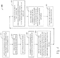
- Figure 4 is a process flow diagram 400 according to several embodiments.
- the process includes photolithographically forming a pillar on a precursor package substrate that includes a laser-drilled via.
- the process includes opening a recess in the precursor package substrate.
- the process includes seating a bridge die in the recess.
- the process includes planarizing a lamination above the precursor package substrate and the bridge die.
- the process includes photolithographically forming a package bond pad on the pillar, a bridge bond pad on the bridge die, and a package-to-bridge trace between the pillar and the bridge-die bond pad to form an EMIB-inclusive semiconductor package.
- the process includes planarizing electrical bumps that contact the EMIB-inclusive semiconductor package at bond pads that couple to the package substrate and to the bridge die.
- the process includes seating a first die and a subsequent die on the planarized electrical bumps to couple each die to the bridge die and to the package substrate to form an EMIB apparatus.
- the process includes assembling the EMIB apparatus to a computing system.
- a computing system 500 includes, but is not limited to, a desktop computer.
- a system 500 includes, but is not limited to a laptop computer.
- a system 500 includes, but is not limited to a netbook.
- a system 500 includes, but is not limited to a tablet.
- a system 500 includes, but is not limited to a notebook computer.
- a system 500 includes, but is not limited to a personal digital assistant (PDA).
- PDA personal digital assistant
- a system 500 includes, but is not limited to a server.
- a system 500 includes, but is not limited to a workstation.
- a system 500 includes, but is not limited to a cellular telephone.
- a system 500 includes, but is not limited to a mobile computing device.
- a system 500 includes, but is not limited to a smart phone.
- a system 500 includes, but is not limited to an internet appliance.
- Other types of computing devices may be configured with the microelectronic device that includes multi-layer solder resist on a semiconductor device package substrate embodiments.
- the processor 510 has one or more processing cores 512 and 512N, where 512N represents the Nth processor core inside processor 510 where N is a positive integer.
- the electronic device system 500 using an EMIB apparatus embodiment that includes multiple processors including 510 and 505, where the processor 505 has logic similar or identical to the logic of the processor 510.
- the processing core 512 includes, but is not limited to, pre-fetch logic to fetch instructions, decode logic to decode the instructions, execution logic to execute instructions and the like.
- the processor 510 has a cache memory 516 to cache at least one of instructions and data for the EMIB apparatus in the system 500.
- the cache memory 516 may be organized into a hierarchal structure including one or more levels of cache memory.
- the processor 510 includes a memory controller 514, which is operable to perform functions that enable the processor 510 to access and communicate with memory 530 that includes at least one of a volatile memory 532 and a non-volatile memory 534.
- the processor 510 is coupled with memory 530 and chipset 520.
- the chipset 520 is part of a system-in-package with an EMIB apparatus depicted in Figure IF.
- the processor 510 may also be coupled to a wireless antenna 578 to communicate with any device configured to at least one of transmit and receive wireless signals.
- the wireless antenna interface 578 operates in accordance with, but is not limited to, the IEEE 802.11 standard and its related family, Home Plug AV (HPAV), Ultra Wide Band (UWB), Bluetooth, WiMax, or any form of wireless communication protocol.
- the volatile memory 532 includes, but is not limited to, Synchronous Dynamic Random Access Memory (SDRAM), Dynamic Random Access Memory (DRAM), RAMBUS Dynamic Random Access Memory (RDRAM), and/or any other type of random access memory device.
- the non-volatile memory 534 includes, but is not limited to, flash memory, phase change memory (PCM), read-only memory (ROM), electrically erasable programmable read-only memory (EEPROM), or any other type of non-volatile memory device.
- the memory 530 stores information and instructions to be executed by the processor 510. In an embodiment, the memory 530 may also store temporary variables or other intermediate information while the processor 510 is executing instructions.
- the chipset 520 connects with processor 510 via Point-to-Point (PtP or P-P) interfaces 517 and 522. Either of these PtP embodiments may be achieved using an EMIB apparatus embodiment as set forth in this disclosure.
- the chipset 520 enables the processor 510 to connect to other elements in an EMIB apparatus embodiment in a system 500.
- interfaces 517 and 522 operate in accordance with a PtP communication protocol such as the Intel® QuickPath Interconnect (QPI) or the like. In other embodiments, a different interconnect may be used.
- the chipset 520 is operable to communicate with the processor 510, 505N, the display device 540, and other devices 572, 576, 574, 560, 562, 564, 566, 577, etc.
- the chipset 520 may also be coupled to a wireless antenna 578 to communicate with any device configured to at least do one of transmit and receive wireless signals.
- the chipset 520 connects to the display device 540 via the interface 526.
- the display 540 may be, for example, a liquid crystal display (LCD), a plasma display, cathode ray tube (CRT) display, or any other form of visual display device.
- the processor 510 and the chipset 520 are merged into an EMIB apparatus in a system.
- the chipset 520 connects to one or more buses 550 and 555 that interconnect various elements 574, 560, 562, 564, and 566. Buses 550 and 555 may be interconnected together via a bus bridge 572 such as at least one EMIB apparatus on a semiconductor device package substrate apparatus embodiment.
- the chipset 520 via interface 524, couples with a non-volatile memory 560, a mass storage device(s) 562, a keyboard/mouse 564, a network interface 566, smart TV 576, and the consumer electronics 577, etc.
- the mass storage device 562 includes, but is not limited to, a solid state drive, a hard disk drive, a universal serial bus flash memory drive, or any other form of computer data storage medium.
- the network interface 566 is implemented by any type of well-known network interface standard including, but not limited to, an Ethernet interface, a universal serial bus (USB) interface, a Peripheral Component Interconnect (PCI) Express interface, a wireless interface and/or any other suitable type of interface.
- the wireless interface operates in accordance with, but is not limited to, the IEEE 802.11 standard and its related family, Home Plug AV (HPAV), Ultra Wide Band (UWB), Bluetooth, WiMax, or any form of wireless communication protocol.
- modules shown in Figure 5 are depicted as separate blocks within the EMIB apparatus embodiment in a computing system 500, the functions performed by some of these blocks may be integrated within a single semiconductor circuit or may be implemented using two or more separate integrated circuits.
- cache memory 516 is depicted as a separate block within processor 510, cache memory 516 (or selected aspects of 516) can be incorporated into the processor core 512.
- the computing system 500 may have a broadcasting structure interface such as for affixing the apparatus to a cellular tower.
- FIG 6 is a cross-section elevation of an EMIB-inclusive semiconductor apparatus 600 with through-silicon via (TSV) access in a bridge die 640 according to an embodiment. Selected reference numbers from Figures 1A through 1F and Figure 3 are included.
- An EMIB package 606 is prepared according to several processing embodiments.
- the bridge die 640 includes at least one TSV 639, and an adhesive 638 is patterned to allow at least one backside bump 641 to contact a trace 622.
- at least one TSV 639' contacts at least one backside bump 641' through the adhesive 638 to contact a bond pad 623 within the EMIB package 606.
- At least one TSV is located directly below the first die 370. In an embodiment, at least one TSV (as depicted in Figure 6 ) is located directly below the subsequent die 372. In an embodiment, at least one TSV (as depicted in Figure 6 ) is located directly below the fourth die 370'.
- Method examples described herein can be machine or computer-implemented at least in part. Some examples can include a computer-readable medium or machine-readable medium encoded with instructions operable to configure an electrical device to perform methods as described in the above examples.
- An implementation of such methods can include code, such as microcode, assembly language code, a higher-level language code, or the like. Such code can include computer readable instructions for performing various methods. The code may form portions of computer program products. Further, in an example, the code can be tangibly stored on one or more volatile, non-transitory, or non-volatile tangible computer-readable media, such as during execution or at other times.
- Examples of these tangible computer-readable media can include, but are not limited to, hard disks, removable magnetic disks, removable optical disks (e.g., compact disks and digital video disks), magnetic cassettes, memory cards or sticks, random access memories (RAMs), read only memories (ROMs), and the like.
Landscapes
- Physics & Mathematics (AREA)
- Geometry (AREA)
- Engineering & Computer Science (AREA)
- Manufacturing & Machinery (AREA)
- Wire Bonding (AREA)
- Production Of Multi-Layered Print Wiring Board (AREA)
- Internal Circuitry In Semiconductor Integrated Circuit Devices (AREA)
Abstract
Description
- This disclosure relates to embedded multi-die interconnect bridge packages that include lithographically formed bumps.
- Semiconductive device miniaturization during packaging has bump-pitch scaling challenges to allow close-pitch electrical bumps to be located on semiconductor device package surfaces.
- Disclosed embodiments are illustrated by way of example, and not by way of limitation, in the figures of the accompanying drawings, where like reference numerals may refer to similar elements, in which:
-
Figure 1A is a cross-section elevation of a semiconductor package substrate during fabrication according to an embodiment; - Figure IB is a cross-section elevation of the precursor package substrate depicted in
Figure 1A after further processing according to an embodiment; -
Figure 1C is a cross-section elevation of the precursor package substrate depicted inFigure 1B after further processing according to an embodiment; -
Figure 1D is cross-section elevation of the precursor package substrate depicted inFigure 1C after further processing according to an embodiment; -
Figure 1E is a cross-section elevation of the precursor package substrate and bridge die after further processing according to an embodiment; -
Figure 1F is a cross-section elevation of an embedded multiple-die interconnect bridge apparatus after further processing of the precursor package substrate and bridge die depicted inFigure 1E according to an embodiment; -
Figure 2 is a detail section taken fromFigure 1F according to an embodiment; -
Figure 3 is a cross-section elevation of an embedded multi-die interconnect bridge-inclusive semiconductor apparatus according to an embodiment; -
Figure 3A is a top view of a of a portion of the EMIB-inclusive semiconductor apparatus depicted inFigure 3 according to an embodiment; -
Figure 4 is a process flow diagram according to several embodiments; -
Figure 5 is included to show an example of a higher-level device application for the disclosed embodiments; and -
Figure 6 is a cross-section elevation of an EMIB-inclusive semiconductor apparatus with through-silicon via access in a bridge die according to an embodiment. - Multi-die semiconductor device packages are assembled and tested through fabrication of a good substrate (KGS), along with known-good silicon bridge (KGB) to achieve high-yield embedded multi-die interconnect bridge (EMIB) semiconductive packaging apparatus.
- Embodiments achieve bump-pitch scaling below 40 micrometer (µm), Accordingly, embedded multiple-die interconnect embodiments may be used for several applications such as for modular die-fabric interconnect (MDFIs).
- Bump-thickness variation is controlled by planarizing both package substrate and silicon bridge bumps after embedding of bridge die in a cavity. Similarly, package-substrate thickness and shrinkage variations are controlled by assembling onto rigid and substantially flat carriers.
-
Figure 1A is a cross-section elevation of asemiconductor package substrate 101 during fabrication according to an embodiment. Aprecursor package substrate 110 includes several layers. Theprecursor package substrate 110 includes aback surface 109 and a precursortop surface 111. Each layer in theprecursor package substrate 110 contains either metallization with interconnects or traces, or it contains dielectric build-up layers for insulation and structural integrity. The metallization layers include layers ofinterconnects traces - In an embodiment, with the four trace layers and the four interconnect layers, the
precursor package substrate 110 may be referred to as a low-layercount package substrate 110. The several build-up layers are not all specifically identified within theprecursor package substrate 110 as they may be formed incidental to the several layers of interconnects and traces. - In an embodiment, the
precursor package substrate 110 is assembled on arigid carrier 128 such as polished glass or polished stainless steel. Therigid carrier 128 has both a rigidity and flatness that is useful to constrain film thickness variations and material shrinkage variations that are low for the design-rule geometries that include about 30 µm bump pitch and lower. - In an embodiment, the
interconnects 112 are plated onto therigid carrier 128 through a first build-uplayer 113 that may have first been laser drilled to form a tapered or frusto-conical recess into which theinterconnects 112 are filled. In an embodiment, a low-loss (low electrical loss) material is used for the ILDs such as a material with glass-fiber reinforcing to impart a useful stiffness to a silicon bridge package substrate. - Forming of the interconnects is carried out by plating processes such as semi-additive plating (SAP) of electronics-grade copper (Cu) to form, e.g. the
tapered interconnects 112. In an embodiment, theinterconnects - Figure IB is a
cross-section elevation 102 of theprecursor package substrate 110 depicted inFigure 1A after further processing according to an embodiment. A plurality of pillars 130 (four occurrences illustrated) is formed ontobond pads 132 that are seated on the precursorpackage top surface 111. Thepillars 130 may also be referred to aspackage pillars 130. Whereas theseveral interconnects Figure 1A ) have substantially frusto-conical (tapered in cross section) shape due to laser drilling of the contact corridors into which the several interconnects are formed, the plurality ofpillars 130 have a substantial right solid-cylinder shape due to forming the plurality ofpillars 130 using photolithography. - In an embodiment, the
several interconnects precursor package substrate 110. The shape and quality of the interconnect recess into which theseveral interconnects - Formation of the plurality of
pillars 130 is done by patterning a photolithographic mask (not pictured), and depositing thepillars 130 such as by electroplating, followed by removing the mask. The plurality of pillars is plated using such processes as semi-additive plating (SAP) in an embodiment. The shape and quality of thepillars 130, can be described as characteristic of photolithographic formation. On characteristic of photolithographic formation includes the substantially right-angle of the solid-cylinder pillars 130. One characteristic of photolithographic formation includes photomicroscopically examining the vertical aspects of thepillars 130 and observing negative-image profiles, that a patterned mask imprints on the pillar walls. In any event within a given known-good substrate that includes a recess to seat a known good bridge die, the right solid-cylinder shape of thepillars 130 is distinguishable from the solid frusto-conical shapes of theseveral interconnects -
Figure 1C is across-section elevation 103 of theprecursor package substrate 110 depicted inFigure 1B after further processing according to an embodiment. Alamination layer 134 has been formed over the plurality ofpillars 130 and on the precursortop surface 111, and abridge recess 136 has been drilled into both thelamination layer 134 and through the precursortop surface 111 until thetrace 122 is uncovered. An adhesive 138 is deposited in thebridge recess 136 and a silicon bridge 140 (also referred to as a bridge die 140) is seated within thebridge recess 136 on theadhesive 138. Although atrace 122 at this level of theprecursor package substrate 110 is depicted as the seat for thesilicon bridge 140, the bridge recess 136 bottoms out above (positive-Z direction) this level according to an embodiment. - Before assembly of the bridge die 140 into the bridge recess 136, the bridge die 140 and the
precursor package substrate 110 are tested, such that a known-good bridge (KGB) 140 is assembled to a known-good-substrate (KGS) 110. Accordingly, yield for an embedded bridge is achieved to useful levels. -
Figure 1D iscross-section elevation 104 of theprecursor package substrate 110 depicted inFigure 1C after further processing according to an embodiment. Anencapsulation material 142 has been filled into thebridge recess 136 and thelamination layer 134 and theencapsulation material 142 have been planarized to a form respective planarizedlaminations planarized lamination layer 135 and theencapsulation material 142, a useful package flatness is achieved for further processing. - In an embodiment,
package bond pads 144, bridge-die bond pads 146 and package-to-bridge traces 148 (only one occurrence illustrated) are plated onto the planarizedlaminations package bond pads 144, the bridge-die bond pads 146 and the package-to-bridge dietraces 148 are plated using such processes as semi-additive plating (SAP) in an embodiment. -
Figure 1E is across-section elevation 105 of theprecursor package substrate 110 andbridge die 140 after further processing according to an embodiment. A patternedphotoresist layer 150 has been formed over thepackage bond pads 144, bridge-die bond pads 146 and package-to-bridge traces 148. In an embodiment, thephotoresist layer 150 has been patterned to partially re-expose thepackage bond pads 144, bridge-die bond pads 146 and package-to-bridge traces 148. In an embodiment, aprotective contact film 152 such as a nickel-palladium-gold (NiPdAu)alloy 152 is plated onto exposed portions of thepackage bond pads 144, bridge-die bond pads 146 and package-to-bridge traces 148. In an embodiment, theprotective contact film 152 provides useful adhesion, low electrical resistivity, and protection from a tin or nickel-tin (Sn or NiSn) bond layer that is to be plated later. -
Figure 1F is across-section elevation 106 of an embedded multiple-die interconnect bridge package (EMIB)package 106 after further processing of theprecursor package substrate 110 and bridge die 140 depicted inFigure 1E according to an embodiment. Plating onto theprotective contact film 152 has been done to include acopper flash layer 154 and on thecopper flash layer 154 the Sn orNiSn bond layer 156 described herein. - After photolithographic formation of the structures above the
top surface 111 of theprecursor package substrate 110, a protective carrier (not pictured) is seated on the exposed structures above thetop surface 111. The rigid carrier 128 (see, e.g.Figure 1E ) is removed and a mid-level interconnect (MLI) 158 and 160 is plated onto theinterconnects 112 that are exposed through theback surface 109 of thefirst ILD layer 113. -
Figure 2 is adetail section 200 taken from a section circle 2 inFigure 1F according to an embodiment. The bridge die 140 includes a bridge-die pillar 162 that is photolithographically formed before the bridge die 140 is seated into thebridge recess 136. In an embodiment, the bridge-die pillar 162 has a diameter 163 (X-direction) of about 10 µm. In an embodiment, formation of thephotoresist layer 150 allows for a bridge-die bond layer 156 to have adiameter 155 of about 20 µm. - In an embodiment, the
protective contact film 152 that is coupled between the bridge-die pillar 158 and thebond layer 156 is also patterned and formed with a diameter of about 10 µm. In an embodiment, the bridge-die bond pads 146 have a diameter of about 25 µm. - In an embodiment, the
bond layer 156 that is plated above thepillar 130 has a diameter of about 40 µm. - Reference is made to
Figure 1F . Via structures formed below (negative-Z direction) the level of the plurality ofpillars 130 have a shape that is characteristic of laser-drilling and SAP formation, while thepillars 130 are formed by litho processing. The micro-vias 120,124 are formed by laser drilling, as indicated by the tapered shape. Via structures above the level of theupper surface 111, including the plurality ofpillars 130 and structures above (positive-Z direction) the pillars have a shape that characteristic of photolithographically patterned vias. -
Figure 3 is a cross-section elevation of an EMIB-inclusive semiconductor apparatus 300 according to an embodiment. Selected reference numbers fromFigures 1A through 1F are included. - In an embodiment, the embedded multiple-die interconnect bridge package (EMIB)
apparatus 106 fromFigure 1F , includes a known-good substrate 110 (seeFigure 1F ) and a known-good bridge 140. TheEMIB apparatus 106 is seated on aninterposer 374. Theinterposer 374 may include routing layers and second level- interconnect (SLI) 392, buildup layers 378 and 380, acore 382 and a mid-level interconnect (MLI)layer 384. - In an embodiment, a
first die 370 and asubsequent die 372 are seated on theEMIB apparatus 106 such that the bridge die 140 provides a communication bridge between theserespective dice dice interposer 374. - In an embodiment, a larger-pitch series of electrical bumps (one instance numbered 386) contacts the
EMIB apparatus 106 in a configuration that allows for such contacts to fan out upon theEMIB apparatus 106. - In an embodiment, a smaller-pitch series of electrical bumps (one instance numbered 388) contacts the known-good bridge die 140 and the respective first and
subsequent dice electrical bumps 388, center-to-center. - In an embodiment before seating the
first die 370 and asubsequent die 372, planarizing is done on the severalelectrical bumps electrical bumps re-planarization level 390. Accordingly, the known-good substrate-containing known-gooddie EMIB apparatus 106 depicted inFigure 1F has been planarized at theupper surface 111, and at the level that supports thepackage bond pads 144, the bridge-die bond pads 146 and the package-to-bridge die traces 148. Similarly and accordingly, re-planarizing of the EMIB-inclusive semiconductor apparatus 300 includes planarizing the severalelectrical bumps re-planarization level 390. - In an embodiment, the
electrical bumps re-planarization level 390, and then thedice electrical bumps electrical bumps - In an embodiment, alignment within EMIB-
inclusive semiconductor apparatus 300 includes plus-or-minus 5 µm for the smaller-bump pitch for theelectrical bumps 386, and plus-or-minus 4.5 µm for Z-direction die bonding variance between the bridge die 140 and any of therespective dice - In an embodiment, the
first die 370 is processor die such as that made by Intel Corporation of Santa Clara, California. In an embodiment, thefirst die 370 is doubled (the doubled die (see the fourth die 370' inFigure 3A ) is disposed in the same X-Z space as the first die, but at a different Y-direction, into or out of the plane of the drawing). With the doubled or fourth die 370', thesubsequent die 372 die is a graphics processor, and thefirst die 370 and the fourth die 370' are logic processors, and thegraphics processor 372 are all coupled to the bridge die 140. - As illustrated, wherein each tapered via 112, 116, 120 and 132 ordinally contacts a
respective trace first trace 114, the second tapered via 116 contacts thesecond trace 118, the third tapered via 120 contacts thethird trace 122, and the fourth tapered via 124 contacts thefourth trace 132. Thefourth trace 132 is disposed at the planarized lamination, and thefourth trace 132 contacts both apackage pillar 130 the fourth tapered via 124. In other words, ordinally sequenced taperedvias traces - In an embodiment after forming
electrical bumps 392 on theinterposer 374, theinterposer 374 is seated on aboard 394 such as amotherboard 394. In an embodiment, theboard 394 includes anexternal shell 396 that provides both physical and electrical insulation for devices within theexternal shell 396. -
Figure 3A is atop plan 301 of a portion of the EMIB-inclusive semiconductor apparatus 300 depicted inFigure 3 according to an embodiment. Selected reference numbers fromFigure 3 is included. - In an embodiment, the
first die 370 and the fourth die 370' are processor dice such as that made by Intel Corporation of Santa Clara, California. In an embodiment, the second die is a graphics processor, and thedice first die 370, thesubsequent die 372 and the bridge die 140 are complemented by the die 370' as a fourth die 370'. In an embodiment, thefirst die 370 and the fourth die 370' are logic processors and thesubsequent die 372 is a graphics processor. -
Figure 4 is a process flow diagram 400 according to several embodiments. - At 410, the process includes photolithographically forming a pillar on a precursor package substrate that includes a laser-drilled via.
- At 420, the process includes opening a recess in the precursor package substrate.
- At 430, the process includes seating a bridge die in the recess.
- At 440, the process includes planarizing a lamination above the precursor package substrate and the bridge die.
- At 450, the process includes photolithographically forming a package bond pad on the pillar, a bridge bond pad on the bridge die, and a package-to-bridge trace between the pillar and the bridge-die bond pad to form an EMIB-inclusive semiconductor package.
- At 460, the process includes planarizing electrical bumps that contact the EMIB-inclusive semiconductor package at bond pads that couple to the package substrate and to the bridge die.
- At 470, the process includes seating a first die and a subsequent die on the planarized electrical bumps to couple each die to the bridge die and to the package substrate to form an EMIB apparatus.
- At 480, the process includes assembling the EMIB apparatus to a computing system.
-
Figure 5 is included to show an example of a higher-level device application for the disclosed embodiments. The EMIB apparatus embodiments may be found in several parts of a computing system. In an embodiment, the EMIB apparatus part of a communications apparatus such as is affixed to a cellular communications tower. In an embodiment, acomputing system 500 includes, but is not limited to, a desktop computer. In an embodiment, asystem 500 includes, but is not limited to a laptop computer. In an embodiment, asystem 500 includes, but is not limited to a netbook. In an embodiment, asystem 500 includes, but is not limited to a tablet. In an embodiment, asystem 500 includes, but is not limited to a notebook computer. In an embodiment, asystem 500 includes, but is not limited to a personal digital assistant (PDA). In an embodiment, asystem 500 includes, but is not limited to a server. In an embodiment, asystem 500 includes, but is not limited to a workstation. In an embodiment, asystem 500 includes, but is not limited to a cellular telephone. In an embodiment, asystem 500 includes, but is not limited to a mobile computing device. In an embodiment, asystem 500 includes, but is not limited to a smart phone. In an embodiment, asystem 500 includes, but is not limited to an internet appliance. Other types of computing devices may be configured with the microelectronic device that includes multi-layer solder resist on a semiconductor device package substrate embodiments. - In an embodiment, the
processor 510 has one ormore processing cores processor 510 where N is a positive integer. In an embodiment, theelectronic device system 500 using an EMIB apparatus embodiment that includes multiple processors including 510 and 505, where theprocessor 505 has logic similar or identical to the logic of theprocessor 510. In an embodiment, theprocessing core 512 includes, but is not limited to, pre-fetch logic to fetch instructions, decode logic to decode the instructions, execution logic to execute instructions and the like. In an embodiment, theprocessor 510 has acache memory 516 to cache at least one of instructions and data for the EMIB apparatus in thesystem 500. Thecache memory 516 may be organized into a hierarchal structure including one or more levels of cache memory. - In an embodiment, the
processor 510 includes amemory controller 514, which is operable to perform functions that enable theprocessor 510 to access and communicate withmemory 530 that includes at least one of avolatile memory 532 and a non-volatile memory 534. In an embodiment, theprocessor 510 is coupled withmemory 530 andchipset 520. In an embodiment, thechipset 520 is part of a system-in-package with an EMIB apparatus depicted in Figure IF. Theprocessor 510 may also be coupled to awireless antenna 578 to communicate with any device configured to at least one of transmit and receive wireless signals. In an embodiment, thewireless antenna interface 578 operates in accordance with, but is not limited to, the IEEE 802.11 standard and its related family, Home Plug AV (HPAV), Ultra Wide Band (UWB), Bluetooth, WiMax, or any form of wireless communication protocol. - In an embodiment, the
volatile memory 532 includes, but is not limited to, Synchronous Dynamic Random Access Memory (SDRAM), Dynamic Random Access Memory (DRAM), RAMBUS Dynamic Random Access Memory (RDRAM), and/or any other type of random access memory device. The non-volatile memory 534 includes, but is not limited to, flash memory, phase change memory (PCM), read-only memory (ROM), electrically erasable programmable read-only memory (EEPROM), or any other type of non-volatile memory device. - The
memory 530 stores information and instructions to be executed by theprocessor 510. In an embodiment, thememory 530 may also store temporary variables or other intermediate information while theprocessor 510 is executing instructions. In the illustrated embodiment, thechipset 520 connects withprocessor 510 via Point-to-Point (PtP or P-P) interfaces 517 and 522. Either of these PtP embodiments may be achieved using an EMIB apparatus embodiment as set forth in this disclosure. Thechipset 520 enables theprocessor 510 to connect to other elements in an EMIB apparatus embodiment in asystem 500. In an embodiment, interfaces 517 and 522 operate in accordance with a PtP communication protocol such as the Intel® QuickPath Interconnect (QPI) or the like. In other embodiments, a different interconnect may be used. - In an embodiment, the
chipset 520 is operable to communicate with theprocessor 510, 505N, thedisplay device 540, andother devices chipset 520 may also be coupled to awireless antenna 578 to communicate with any device configured to at least do one of transmit and receive wireless signals. - The
chipset 520 connects to thedisplay device 540 via theinterface 526. Thedisplay 540 may be, for example, a liquid crystal display (LCD), a plasma display, cathode ray tube (CRT) display, or any other form of visual display device. In an embodiment, theprocessor 510 and thechipset 520 are merged into an EMIB apparatus in a system. Additionally, thechipset 520 connects to one ormore buses various elements Buses bus bridge 572 such as at least one EMIB apparatus on a semiconductor device package substrate apparatus embodiment. In an embodiment, thechipset 520, viainterface 524, couples with anon-volatile memory 560, a mass storage device(s) 562, a keyboard/mouse 564, anetwork interface 566,smart TV 576, and theconsumer electronics 577, etc. - In an embodiment, the
mass storage device 562 includes, but is not limited to, a solid state drive, a hard disk drive, a universal serial bus flash memory drive, or any other form of computer data storage medium. In one embodiment, thenetwork interface 566 is implemented by any type of well-known network interface standard including, but not limited to, an Ethernet interface, a universal serial bus (USB) interface, a Peripheral Component Interconnect (PCI) Express interface, a wireless interface and/or any other suitable type of interface. In one embodiment, the wireless interface operates in accordance with, but is not limited to, the IEEE 802.11 standard and its related family, Home Plug AV (HPAV), Ultra Wide Band (UWB), Bluetooth, WiMax, or any form of wireless communication protocol. - While the modules shown in
Figure 5 are depicted as separate blocks within the EMIB apparatus embodiment in acomputing system 500, the functions performed by some of these blocks may be integrated within a single semiconductor circuit or may be implemented using two or more separate integrated circuits. For example, althoughcache memory 516 is depicted as a separate block withinprocessor 510, cache memory 516 (or selected aspects of 516) can be incorporated into theprocessor core 512. - Where useful, the
computing system 500 may have a broadcasting structure interface such as for affixing the apparatus to a cellular tower. -
Figure 6 is a cross-section elevation of an EMIB-inclusive semiconductor apparatus 600 with through-silicon via (TSV) access in a bridge die 640 according to an embodiment. Selected reference numbers fromFigures 1A through 1F andFigure 3 are included. AnEMIB package 606 is prepared according to several processing embodiments. - In an embodiment, the bridge die 640 includes at least one
TSV 639, and an adhesive 638 is patterned to allow at least onebackside bump 641 to contact atrace 622. In an embodiment, at least one TSV 639' contacts at least one backside bump 641' through the adhesive 638 to contact abond pad 623 within theEMIB package 606. - Where direct contact from the bridge die 640 into the
EMIB package 606 includes package-to-bridge traces 148, disclosedTSV embodiments 639 and 639' allow for direct contact through the bridge die 640 backside into theEMIB package 606. - Reference is made to
Figure 3A . In an embodiment at least one TSV (as depicted inFigure 6 ) is located directly below thefirst die 370. In an embodiment, at least one TSV (as depicted inFigure 6 ) is located directly below thesubsequent die 372. In an embodiment, at least one TSV (as depicted inFigure 6 ) is located directly below the fourth die 370'. - To illustrate the EMIB apparatus embodiments and methods disclosed herein, a non-limiting list of examples is provided herein:
- Example 1 is a semiconductor package apparatus, comprising: a bridge die disposed in a recess of a semiconductor package substrate, wherein the semiconductor package substrate includes filled via characteristic of laser drilling coupled to a package pillar characteristic of photolighographic patterning; a planarized lamination above the package pillar and the bridge die, wherein the bridge die includes a bridge-die bond pad; a planarized electrical bump that is coupled to the package pillar and a planarized electrical bump that is coupled to the bridge-die bond pad; a first semiconductive device coupled to the planarized electrical bump that is coupled to the package pillar; and a subsequent semiconductive device coupled to the planarized electrical bump that is coupled to the bridge-die bond pad.
- In Example 2, the subject matter of Example 1 optionally includes a package bond pad patterned on the planarized lamination and contacting the package pillar; a bridge-die bond pad patterned on the planarized lamination and contacting a bridge-die pillar; and a package-to-bridge trace patterned on the planarized lamination and contacting a bridge-die pillar and a package pillar.
- In Example 3, the subject matter of any one or more of Examples 1-2 optionally include a package bond pad patterned on the planarized lamination and contacting the package pillar; a bridge-die bond pad patterned on the planarized lamination and contacting a bridge-die pillar; a package-to-bridge trace patterned on the planarized lamination and contacting a bridge-die pillar and a package pillar; and a protective contact film disposed on each of the package bond pad and the bridge-to-die bond pad and patterned through a patterned photoresist layer.
- In Example 4, the subject matter of any one or more of Examples 1-3 optionally include a package bond pad patterned on the planarized lamination and contacting the package pillar; a bridge-die bond pad patterned on the planarized lamination and contacting a bridge-die pillar; and a package-to-bridge trace patterned on the planarized lamination and contacting a bridge-die pillar and a package pillar, wherein the bridge die is seated on an adhesive, and wherein the package bond pad and the bridge-die bond pad exhibit planarization above the patterned photoresist.
- In Example 5, the subject matter of any one or more of Examples 1-4 optionally include wherein the bridge die is seated on an adhesive, and wherein the package bond pad and the bridge-die bond pad exhibit planarization above the patterned photoresist.
- In Example 6, the subject matter of any one or more of Examples 1-5 optionally include wherein the bridge die is seated on an adhesive, and wherein the package bond pad and the bridge-die bond pad exhibit planarization above the patterned photoresist, further including a mid-level interconnect on the back surface, wherein the mid-level interconnect contacts a tapered via within the semiconductor package substrate.
- In Example 7, the subject matter of any one or more of Examples 1-6 optionally include wherein the semiconductor package substrate includes a back surface, further including: a mid-level interconnect on the back surface, wherein the mid-level interconnect contacts a tapered via within the semiconductor package substrate.
- In Example 8, the subject matter of any one or more of Examples 1-7 optionally include wherein the semiconductor package substrate includes a back surface, further including: a mid-level interconnect on the back surface, wherein the mid-level interconnect contacts a tapered via; and an interposer coupled to the mid-level interconnect.
- In Example 9, the subject matter of any one or more of Examples 1-8 optionally include wherein the semiconductor package substrate includes a back surface, further including: a mid-level interconnect on the back surface, wherein the mid-level interconnect contacts a tapered via; an interposer coupled to the mid-level interconnect; a ball-grid array on the interposer; and a board coupled to the ball-grid array.
- In Example 10, the subject matter of any one or more of Examples 1-9 optionally include wherein the semiconductor package substrate includes a back surface, further including: a mid-level interconnect on the back surface, wherein the mid-level interconnect contacts a tapered via, and wherein the semiconductor package substrate includes a first tapered via, a second tapered via, a third tapered via and a fourth tapered via and a first trace, a second trace, a third trace and a fourth trace, wherein each tapered via ordinally contacts a trace, and wherein the fourth trace is disposed at the planarized lamination, and wherein the fourth trace contacts the package pillar one of the fourth tapered via.
- In Example 11, the subject matter of any one or more of Examples 1-10 optionally include a fourth die, wherein the first die, the subsequent die and the fourth die each is coupled to the bridge die.
- In Example 12, the subject matter of any one or more of Examples 1-11 optionally include wherein the semiconductor package substrate includes four tapered vias that ordinally contact four respective ordinally sequenced traces, and wherein the fourth trace also contacts a package pillar.
- Example 13 is a process of forming a semiconductor package apparatus, comprising: photolithographically forming a package pillar on a precursor package substrate, to couple the package pillar with a laser-drilled via; seating a bridge die in a recess in the precursor package substrate; forming a planarized lamination above the precursor package substrate and the bridge die; forming planarized electrical bumps that couple to the precursor package substrate and to the bridge die; and seating a first semiconductive device and a subsequent semiconductive device on the planarized electrical bumps, under conditions that the bridge die provides a communications bridge between the first and subsequent semiconductive dice.
- In Example 14, the subject matter of Example 13 optionally includes wherein photolithographically forming the package pillar on the precursor package substrate includes forming the package pillar on a trace that contacts the package pillar with a laser-drilled via.
- In Example 15, the subject matter of any one or more of Examples 13-14 optionally include filling the recess with a lamination after seating the bridge die, followed by forming the planarized lamination above the precursor package substrate and the bridge die.
- In Example 16, the subject matter of any one or more of Examples 13-15 optionally include seating the precursor package substrate on a carrier; forming package bond pads and bridge-die bond pads on the planarized lamination; patterning a photoresist layer on the planarized lamination; patterning a bond layer through the photoresist to couple to the pillar and to the bridge-die; and forming solder-paste electrical bumps on the bond layers, followed by forming the planarized electrical bumps.
- In Example 17, the subject matter of any one or more of Examples 13-16 optionally include bonding the first and subsequent dice on the planarized electrical bumps by using added heat and pressure.
- Example 18 is a computing system, comprising: a bridge die disposed in a recess of a semiconductor package substrate, wherein the semiconductor package substrate includes filled via characteristic of laser drilling coupled to a package pillar characteristic of photolighographic patterning; a planarized lamination above the package pillar and the bridge die, wherein the bridge die includes a bridge-die bond pad; a planarized electrical bump coupled to the package pillar and a planarized electrical bump that is coupled to the bridge-die bond pad; a first semiconductive device coupled to the planarized electrical bump coupled to the package pillar; a subsequent semiconductive device coupled to the planarized electrical bump that is coupled to the bridge-die bond pad; a mid-level interconnect on a surface of the semiconductor package substrate, wherein the mid-level interconnect contacts a tapered via; an interposer coupled to the mid-level interconnect; and a board coupled to the interposer, wherein the board includes an external shell.
- In Example 19, the subject matter of Example 18 optionally includes wherein the bridge die is coupled to a chipset.
- In Example 20, the subject matter of any one or more of Examples 18-19 optionally include wherein the subsequent die is a graphics processor, further including a fourth die also coupled to the bridge die, wherein the first die and the fourth die are logic processors.
- Example 21 is a semiconductor package apparatus, comprising: a bridge die disposed in a recess of a semiconductor package substrate, wherein the semiconductor package substrate includes filled via characteristic of laser drilling coupled to a package pillar characteristic of photolighographic patterning; at least one through-silicon via (TSV) that communicates through the bridge die to couple with at least one of a trace and a bond pad within the semiconductor package substrate.
- In Example 22, the subject matter of Example 21 optionally includes wherein the at least one TSV is coupled to one selected from a trace and a bond pad in the semiconductor package substrate.
- In Example 23, the subject matter of any one or more of Examples 21-22 optionally include a fourth die, wherein the first die, the subsequent die and the fourth die each is coupled to the bridge die.
- The above detailed description includes references to the accompanying drawings, which form a part of the detailed description. The drawings show, by way of illustration, specific embodiments in which the invention can be practiced. These embodiments are also referred to herein as "examples." Such examples can include elements in addition to those shown or described. However, the present inventors also contemplate examples in which only those elements shown or described are provided. Moreover, the present inventors also contemplate examples using any combination or permutation of those elements shown or described (or one or more aspects thereof), either with respect to a particular example (or one or more aspects thereof), or with respect to other examples (or one or more aspects thereof) shown or described herein.
- In the event of inconsistent usages between this document and any documents so incorporated by reference, the usage in this document controls.
- In this document, the terms "a" or "an" are used, as is common in patent documents, to include one or more than one, independent of any other instances or usages of "at least one" or "one or more." In this document, the term "or" is used to refer to a nonexclusive or, such that "A or B" includes "A but not B," "B but not A," and "A and B," unless otherwise indicated. In this document, the terms "including" and "in which" are used as the plain-English equivalents of the respective terms "comprising" and "wherein." Connections within disclosed embodiments may be described as "coupled" and "contacting" or the like, where "coupled" means electrical or thermal communication is between the two named structures, and "contacting" or "contacts" means the two named structures physically touch. Also, in the following claims, the terms "including" and "comprising" are open-ended, that is, a system, device, article, composition, formulation, or process that includes elements in addition to those listed after such a term in a claim are still deemed to fall within the scope of that claim. Moreover, in the following claims, the terms "first," "second," and "third," etc. are used merely as labels, and are not intended to impose numerical requirements on their objects.
- Method examples described herein can be machine or computer-implemented at least in part. Some examples can include a computer-readable medium or machine-readable medium encoded with instructions operable to configure an electrical device to perform methods as described in the above examples. An implementation of such methods can include code, such as microcode, assembly language code, a higher-level language code, or the like. Such code can include computer readable instructions for performing various methods. The code may form portions of computer program products. Further, in an example, the code can be tangibly stored on one or more volatile, non-transitory, or non-volatile tangible computer-readable media, such as during execution or at other times. Examples of these tangible computer-readable media can include, but are not limited to, hard disks, removable magnetic disks, removable optical disks (e.g., compact disks and digital video disks), magnetic cassettes, memory cards or sticks, random access memories (RAMs), read only memories (ROMs), and the like.
- The above description is intended to be illustrative, and not restrictive. For example, the above-described examples (or one or more aspects thereof) may be used in combination with each other. Other embodiments can be used, such as by one of ordinary skill in the art upon reviewing the above description. The Abstract is provided to comply with 37 C.F.R. § 1.72(b), to allow the reader to quickly ascertain the nature of the technical disclosure. It is submitted with the understanding that it will not be used to interpret or limit the scope or meaning of the claims. Also, in the above Detailed Description, various features may be grouped together to streamline the disclosure. This should not be interpreted as intending that an unclaimed disclosed feature is essential to any claim. Rather, inventive subject matter may lie in less than all features of a particular disclosed embodiment. Thus, the following claims are hereby incorporated into the Detailed Description as examples or embodiments, with each claim standing on its own as a separate embodiment, and it is contemplated that such embodiments can be combined with each other in various combinations or permutations. The scope of the disclosed embodiments should be determined with reference to the appended claims, along with the full scope of equivalents to which such claims are entitled.
Claims (15)
- A semiconductor package apparatus, comprising:a bridge die disposed in a recess of a semiconductor package substrate, wherein the semiconductor package substrate includes filled via characteristic of laser drilling coupled to a package pillar characteristic of photolighographic patterning;at least one through-silicon via (TSV) that communicates through the bridge die to couple with at least one of a trace and a bond pad within the semiconductor package substrate;a planarized lamination above the package pillar and the bridge die, wherein the bridge die includes a bridge-die bond pad;a planarized electrical bump that is coupled to the package pillar and a planarized electrical bump that is coupled to the bridge-die bond pad;a first semiconductive device coupled to the planarized electrical bump that is coupled to the package pillar;a subsequent semiconductive device coupled to the planarized electrical bump that is coupled to the bridge-die bond pad;a package bond pad patterned on the planarized lamination and contacting the package pillar;a bridge-die bond pad patterned on the planarized lamination and contacting a bridge-die pillar; anda package-to-bridge trace patterned on the planarized lamination and contacting a bridge-die pillar and a package pillar.
- The semiconductor package of claim 1, wherein the bridge die is seated on an adhesive, and wherein the package bond pad and the bridge-die bond pad exhibit planarization above the patterned photoresist.
- The semiconductor package of claim 1, wherein the semiconductor package substrate includes a back surface, further including:a mid-level interconnect on the back surface, wherein the mid-level interconnect contacts a tapered via within the semiconductor package substrate.
- The semiconductor package of claim 1, wherein the semiconductor package substrate includes a back surface, further including:a mid-level interconnect on the back surface, wherein the mid-level interconnect contacts a tapered via; andan interposer coupled to the mid-level interconnect.
- The semiconductor package of claim 1, wherein the semiconductor package substrate includes a back surface, further including: amid-level interconnect on the back surface, wherein the mid-level interconnect contacts a tapered via;an interposer coupled to the mid-level interconnect;a ball-grid array on the interposer; anda board coupled to the ball-grid array.
- The semiconductor package of claim 1, wherein the semiconductor package substrate includes a back surface, further including:a mid-level interconnect on the back surface, wherein the mid-level interconnect contacts a tapered via, and wherein the semiconductor package substrate includes a first tapered via, a second tapered via, a third tapered via and a fourth tapered via and a first trace, a second trace, a third trace and a fourth trace, wherein each tapered via ordinally contacts a trace, and wherein the fourth trace is disposed at the planarized lamination, and wherein the fourth trace contacts the package pillar one of the fourth tapered via.
- The semiconductor package of claim 1, further including a fourth die,
wherein the first die, the subsequent die and the fourth die each is coupled to the bridge die. - The semiconductor package of claim 1, wherein the semiconductor package substrate includes four tapered vias that ordinally contact four respective ordinally sequenced traces, and wherein the fourth trace also contacts a package pillar.
- A process of forming a semiconductor package apparatus, comprising:photolithographically forming a package pillar on a precursor package substrate, to couple the package pillar with a laser-drilled via;seating a bridge die in a recess in the precursor package substrate;forming a planarized lamination above the precursor package substrate and the bridge die;forming planarized electrical bumps that couple to the precursor package substrate and to the bridge die; andseating a first semiconductive device and a subsequent semiconductive device on the planarized electrical bumps, under conditions that the bridge die provides a communications bridge between the first and subsequent semiconductive dice.
- The process of claim 9, wherein photolithographically forming the package pillar on the precursor package substrate includes forming the package pillar on a trace that contacts the package pillar with a laser-drilled via.
- The process of claim 9, further including:filling the recess with a lamination after seating the bridge die, followed by forming the planarized lamination above the precursor package substrate and the bridge die.
- The process of claim 9, further including:seating the precursor package substrate on a carrier;forming package bond pads and bridge-die bond pads on the planarized lamination;patterning a photoresist layer on the planarized lamination;patterning a bond layer through the photoresist to couple to the pillar and to the bridge-die; andforming solder-paste electrical bumps on the bond layers, followed by forming the planarized electrical bumps.
- A computing system, comprising:a bridge die disposed in a recess of a semiconductor package substrate, wherein the semiconductor package substrate includes filled via characteristic of laser drilling coupled to a package pillar characteristic of photolighographic patterning;a planarized lamination above the package pillar and the bridge die, wherein the bridge die includes a bridge-die bond pad;a planarized electrical bump coupled to the package pillar and a planarized electrical bump that is coupled to the bridge-die bond pad;a first semiconductive device coupled to the planarized electrical bump coupled to the package pillar;a subsequent semiconductive device coupled to the planarized electrical bump that is coupled to the bridge-die bond pad;a mid-level interconnect on a surface of the semiconductor package substrate, wherein the mid-level interconnect contacts a tapered via;an interposer coupled to the mid-level interconnect; anda board coupled to the interposer, wherein the board includes an external shell.
- The computing system of claim 13, wherein the bridge die is coupled to a chipset.
- The computing system of claim 13, wherein the subsequent die is a graphics processor, further including a fourth die also coupled to the bridge die, wherein the first die and the fourth die are logic processors.
Applications Claiming Priority (1)
| Application Number | Priority Date | Filing Date | Title |
|---|---|---|---|
| US15/853,330 US10163798B1 (en) | 2017-12-22 | 2017-12-22 | Embedded multi-die interconnect bridge packages with lithotgraphically formed bumps and methods of assembling same |
Publications (1)
| Publication Number | Publication Date |
|---|---|
| EP3503171A1 true EP3503171A1 (en) | 2019-06-26 |
Family
ID=64453300
Family Applications (1)
| Application Number | Title | Priority Date | Filing Date |
|---|---|---|---|
| EP18207616.6A Pending EP3503171A1 (en) | 2017-12-22 | 2018-11-21 | Embedded multi-die interconnect bridge packages with lithotgraphically formed bump pitches and methods of assembling same |
Country Status (3)
| Country | Link |
|---|---|
| US (4) | US10163798B1 (en) |
| EP (1) | EP3503171A1 (en) |
| CN (1) | CN109962055B (en) |
Cited By (2)
| Publication number | Priority date | Publication date | Assignee | Title |
|---|---|---|---|---|
| US20230062138A1 (en) * | 2021-08-30 | 2023-03-02 | Taiwan Semiconductor Manufacturing Company, Ltd. | Semiconductor package structure and method for forming the same |
| GB2603404B (en) * | 2019-10-04 | 2024-06-26 | Ibm | Alignment carrier for interconnect bridge assembly |
Families Citing this family (88)
| Publication number | Priority date | Publication date | Assignee | Title |
|---|---|---|---|---|
| US8227904B2 (en) * | 2009-06-24 | 2012-07-24 | Intel Corporation | Multi-chip package and method of providing die-to-die interconnects in same |
| US10950550B2 (en) * | 2015-12-22 | 2021-03-16 | Intel Corporation | Semiconductor package with through bridge die connections |
| US11625523B2 (en) | 2016-12-14 | 2023-04-11 | iCometrue Company Ltd. | Logic drive based on standard commodity FPGA IC chips |
| TW202537391A (en) | 2016-12-14 | 2025-09-16 | 成真股份有限公司 | Logic drive based on standard commodity fpga ic chips |
| US10447274B2 (en) | 2017-07-11 | 2019-10-15 | iCometrue Company Ltd. | Logic drive based on standard commodity FPGA IC chips using non-volatile memory cells |
| US20190035715A1 (en) * | 2017-07-31 | 2019-01-31 | Innolux Corporation | Package device and manufacturing method thereof |
| US10957679B2 (en) | 2017-08-08 | 2021-03-23 | iCometrue Company Ltd. | Logic drive based on standardized commodity programmable logic semiconductor IC chips |
| US10630296B2 (en) | 2017-09-12 | 2020-04-21 | iCometrue Company Ltd. | Logic drive with brain-like elasticity and integrality based on standard commodity FPGA IC chips using non-volatile memory cells |
| CN116666332A (en) * | 2017-09-28 | 2023-08-29 | 英特尔公司 | Power Delivery Using Trench Structured Embedded Bridge Die |
| US10651126B2 (en) * | 2017-12-08 | 2020-05-12 | Applied Materials, Inc. | Methods and apparatus for wafer-level die bridge |
| US10163798B1 (en) | 2017-12-22 | 2018-12-25 | Intel Corporation | Embedded multi-die interconnect bridge packages with lithotgraphically formed bumps and methods of assembling same |
| US10608642B2 (en) | 2018-02-01 | 2020-03-31 | iCometrue Company Ltd. | Logic drive using standard commodity programmable logic IC chips comprising non-volatile radom access memory cells |
| US10623000B2 (en) | 2018-02-14 | 2020-04-14 | iCometrue Company Ltd. | Logic drive using standard commodity programmable logic IC chips |
| US10580738B2 (en) * | 2018-03-20 | 2020-03-03 | International Business Machines Corporation | Direct bonded heterogeneous integration packaging structures |
| US10872862B2 (en) * | 2018-03-29 | 2020-12-22 | Taiwan Semiconductor Manufacturing Company, Ltd. | Package structure having bridge structure for connection between semiconductor dies and method of fabricating the same |
| US10608638B2 (en) | 2018-05-24 | 2020-03-31 | iCometrue Company Ltd. | Logic drive using standard commodity programmable logic IC chips |
| US12476637B2 (en) | 2018-05-24 | 2025-11-18 | iCometrue Company Ltd. | Logic drive using standard commodity programmable logic IC chips |
| US11309334B2 (en) | 2018-09-11 | 2022-04-19 | iCometrue Company Ltd. | Logic drive using standard commodity programmable logic IC chips comprising non-volatile random access memory cells |
| US10937762B2 (en) | 2018-10-04 | 2021-03-02 | iCometrue Company Ltd. | Logic drive based on multichip package using interconnection bridge |
| US11616046B2 (en) | 2018-11-02 | 2023-03-28 | iCometrue Company Ltd. | Logic drive based on chip scale package comprising standardized commodity programmable logic IC chip and memory IC chip |
| US11211334B2 (en) | 2018-11-18 | 2021-12-28 | iCometrue Company Ltd. | Logic drive based on chip scale package comprising standardized commodity programmable logic IC chip and memory IC chip |
| US10667399B1 (en) * | 2018-11-27 | 2020-05-26 | Nokia Solutions And Networks Oy | Discrete component carrier |
| US11652060B2 (en) | 2018-12-28 | 2023-05-16 | Intel Corporation | Die interconnection scheme for providing a high yielding process for high performance microprocessors |
| US10998262B2 (en) * | 2019-04-15 | 2021-05-04 | Intel Corporation | Stripped redistrubution-layer fabrication for package-top embedded multi-die interconnect bridge |
| IT201900006740A1 (en) * | 2019-05-10 | 2020-11-10 | Applied Materials Inc | SUBSTRATE STRUCTURING PROCEDURES |
| US11735533B2 (en) | 2019-06-11 | 2023-08-22 | Intel Corporation | Heterogeneous nested interposer package for IC chips |
| US11133256B2 (en) | 2019-06-20 | 2021-09-28 | Intel Corporation | Embedded bridge substrate having an integral device |
| US11227838B2 (en) | 2019-07-02 | 2022-01-18 | iCometrue Company Ltd. | Logic drive based on multichip package comprising standard commodity FPGA IC chip with cooperating or supporting circuits |
| KR102798702B1 (en) * | 2019-07-22 | 2025-04-23 | 삼성전자주식회사 | Semiconductor package |
| US11694959B2 (en) * | 2019-07-29 | 2023-07-04 | Intel Corporation | Multi-die ultrafine pitch patch architecture and method of making |
| US11600567B2 (en) * | 2019-07-31 | 2023-03-07 | Advanced Semiconductor Engineering, Inc. | Semiconductor device package and method for manufacturing the same |
| US11887930B2 (en) | 2019-08-05 | 2024-01-30 | iCometrue Company Ltd. | Vertical interconnect elevator based on through silicon vias |
| KR102930384B1 (en) * | 2019-08-12 | 2026-02-23 | 삼성전자주식회사 | Semiconductor package |
| TWI710090B (en) * | 2019-09-06 | 2020-11-11 | 力成科技股份有限公司 | Semiconductor package structure and manufacturing method thereof |
| US11637056B2 (en) | 2019-09-20 | 2023-04-25 | iCometrue Company Ltd. | 3D chip package based on through-silicon-via interconnection elevator |
| EP3799539B1 (en) * | 2019-09-27 | 2022-03-16 | Siemens Aktiengesellschaft | Circuit carrier, package and method for its production |
| US11264314B2 (en) * | 2019-09-27 | 2022-03-01 | International Business Machines Corporation | Interconnection with side connection to substrate |
| TWI726500B (en) * | 2019-11-25 | 2021-05-01 | 東捷科技股份有限公司 | Manufacturing method of package structure |
| KR102762887B1 (en) * | 2019-12-10 | 2025-02-07 | 삼성전기주식회사 | Substrate with electronic component embedded therein |
| KR102776282B1 (en) * | 2019-12-16 | 2025-03-07 | 삼성전기주식회사 | Substrate with electronic component embedded therein |
| TWI795700B (en) * | 2019-12-20 | 2023-03-11 | 台灣積體電路製造股份有限公司 | Integrated circuit package and method forming same |
| US11616026B2 (en) * | 2020-01-17 | 2023-03-28 | Taiwan Semiconductor Manufacturing Company, Ltd. | Semiconductor device and method of manufacture |
| US11600526B2 (en) | 2020-01-22 | 2023-03-07 | iCometrue Company Ltd. | Chip package based on through-silicon-via connector and silicon interconnection bridge |
| US12272650B2 (en) | 2020-02-28 | 2025-04-08 | Intel Corporation | Microelectronic package with substrate cavity for bridge-attach |
| US12176268B2 (en) * | 2020-03-24 | 2024-12-24 | Intel Corporation | Open cavity bridge co-planar placement architectures and processes |
| US11948877B2 (en) * | 2020-03-31 | 2024-04-02 | Qualcomm Incorporated | Hybrid package apparatus and method of fabricating |
| US11670596B2 (en) * | 2020-04-07 | 2023-06-06 | Mediatek Inc. | Semiconductor package structure |
| US11955448B2 (en) * | 2020-05-21 | 2024-04-09 | Intel Corporation | Architecture to manage FLI bump height delta and reliability needs for mixed EMIB pitches |
| US11923307B2 (en) * | 2020-06-16 | 2024-03-05 | Intel Corporation | Microelectronic structures including bridges |
| US11887962B2 (en) | 2020-06-16 | 2024-01-30 | Intel Corporation | Microelectronic structures including bridges |
| KR102883706B1 (en) | 2020-06-30 | 2025-11-11 | 삼성전자주식회사 | Semiconductor package |
| US11705378B2 (en) * | 2020-07-20 | 2023-07-18 | Taiwan Semiconductor Manufacturing Company, Ltd. | Semiconductor packages and methods of forming the same |
| KR102854175B1 (en) * | 2020-07-31 | 2025-09-03 | 삼성전기주식회사 | Printed circuit board and manufacturing method for the same |
| US11676940B2 (en) * | 2020-08-12 | 2023-06-13 | Advanced Micro Devices, Inc. | Hybrid bonded interconnect bridging |
| US11395408B2 (en) * | 2020-08-28 | 2022-07-19 | Apple Inc. | Wafer-level passive array packaging |
| EP3975226A1 (en) * | 2020-09-28 | 2022-03-30 | Infineon Technologies Austria AG | A semiconductor device module comprising vertical metallic contacts and a method for fabricating the same |
| US11587896B2 (en) | 2020-12-09 | 2023-02-21 | International Business Machines Corporation | Transferrable pillar structure for fanout package or interconnect bridge |
| US12327797B2 (en) | 2020-12-16 | 2025-06-10 | Intel Corporation | Microelectronic structures including glass cores |
| US12243792B2 (en) * | 2020-12-21 | 2025-03-04 | Intel Corporation | Microelectronic structures including bridges |
| EP4016618B1 (en) * | 2020-12-21 | 2025-01-29 | Hamilton Sundstrand Corporation | Power device packaging |
| TW202240808A (en) | 2021-01-08 | 2022-10-16 | 成真股份有限公司 | Micro heat pipes for use in integrated circuit chip package |
| US20220310518A1 (en) * | 2021-03-25 | 2022-09-29 | Intel Corporation | Embedded bridge architecture with thinned surface |
| US11735529B2 (en) | 2021-05-21 | 2023-08-22 | International Business Machines Corporation | Side pad anchored by next adjacent via |
| US12176278B2 (en) | 2021-05-30 | 2024-12-24 | iCometrue Company Ltd. | 3D chip package based on vertical-through-via connector |
| US12230564B2 (en) * | 2021-06-11 | 2025-02-18 | Intel Corporation | Package substrate z-disaggregation with liquid metal interconnects |
| US12255163B2 (en) * | 2021-08-12 | 2025-03-18 | Micron Technology, Inc. | Bond pads for semiconductor die assemblies and associated methods and systems |
| US12261102B2 (en) * | 2021-08-30 | 2025-03-25 | Taiwan Semiconductor Manufacturing Company, Ltd. | Semiconductor package and method of forming the same |
| US11862597B2 (en) | 2021-09-23 | 2024-01-02 | Apple Inc. | Asymmetric stackup structure for SoC package substrates |
| US12268012B2 (en) | 2021-09-24 | 2025-04-01 | iCometrue Company Ltd. | Multi-output look-up table (LUT) for use in coarse-grained field-programmable-gate-array (FPGA) integrated-circuit (IC) chip |
| US20230187365A1 (en) | 2021-09-24 | 2023-06-15 | iCometrue Company Ltd. | Field Programmable Multichip Package Based on Field-Programmable-Gate-Array (FPGA) Integrated-Circuit (IC) Chip |
| KR20230067337A (en) | 2021-11-09 | 2023-05-16 | 삼성전자주식회사 | Semiconductor package and method of manufacturing the same |
| US12165956B2 (en) | 2021-12-08 | 2024-12-10 | Apple Inc. | Molded silicon on passive package |
| US20230187386A1 (en) * | 2021-12-14 | 2023-06-15 | Intel Corporation | Microelectronic assemblies with glass substrates and planar inductors |
| US12412868B2 (en) | 2021-12-21 | 2025-09-09 | Intel Corporation | Microelectronic assemblies including interconnects with different solder materials |
| US20230207439A1 (en) * | 2021-12-23 | 2023-06-29 | Adel A. Elsherbini | Package architecture with in-glass blind and through cavities to accommodate dies |
| CN116417403A (en) * | 2021-12-30 | 2023-07-11 | 联华电子股份有限公司 | Semiconductor element and manufacturing method thereof |
| US12431408B2 (en) | 2022-01-10 | 2025-09-30 | International Business Machines Corporation | TSV and backside power distribution structure |
| US12588525B2 (en) | 2022-03-23 | 2026-03-24 | Taiwan Semiconductor Manufacturing Company Limited | Packaging substrate including an underfill injection opening and methods of forming the same |
| US12568834B2 (en) | 2022-06-15 | 2026-03-03 | Google Llc | Active silicon D2D bridge |
| US20240030204A1 (en) * | 2022-07-22 | 2024-01-25 | Intel Corporation | Multi-die panel-level high performance computing components |
| KR20240018263A (en) | 2022-08-02 | 2024-02-13 | 삼성전기주식회사 | Printed circuit board |
| CN115274475B (en) * | 2022-09-27 | 2022-12-16 | 江苏芯德半导体科技有限公司 | Chip packaging method with high-density connecting layer and chip packaging structure thereof |
| US20240213235A1 (en) * | 2022-12-27 | 2024-06-27 | Intel Corporation | Architectures for backside power delivery with stacked integrated circuit devices |
| US20240213163A1 (en) * | 2022-12-27 | 2024-06-27 | Intel Corporation | Interconnect device and method |
| US12431410B2 (en) * | 2023-01-06 | 2025-09-30 | Nanya Technology Corporation | Semiconductor device with polymer liner and method for fabricating the same |
| US12406933B2 (en) * | 2023-02-22 | 2025-09-02 | Nanya Technology Corporation | Semiconductor device including through-insulator via structure |
| US20240332195A1 (en) * | 2023-04-02 | 2024-10-03 | Intel Corporation | Spray-coated photoresist and photoimageable dielectrics to enable tsv bridge for glass core packages |
| CN116403988B (en) * | 2023-06-07 | 2023-08-29 | 天芯电子科技(南京)有限公司 | An embedded multi-chip packaging substrate |
Citations (2)
| Publication number | Priority date | Publication date | Assignee | Title |
|---|---|---|---|---|
| US20160095219A1 (en) * | 2014-09-25 | 2016-03-31 | Ibiden Co., Ltd. | Printed wiring board and semiconductor device having the same |
| WO2017111957A1 (en) * | 2015-12-22 | 2017-06-29 | Intel Corporation | Semiconductor package with through bridge die connections |
Family Cites Families (35)
| Publication number | Priority date | Publication date | Assignee | Title |
|---|---|---|---|---|
| US8064224B2 (en) * | 2008-03-31 | 2011-11-22 | Intel Corporation | Microelectronic package containing silicon patches for high density interconnects, and method of manufacturing same |
| US8508037B2 (en) * | 2010-12-07 | 2013-08-13 | Intel Corporation | Bumpless build-up layer and laminated core hybrid structures and methods of assembling same |
| CN102244061A (en) * | 2011-07-18 | 2011-11-16 | 江阴长电先进封装有限公司 | Low-k chip package structure |
| US9412689B2 (en) * | 2012-01-24 | 2016-08-09 | Taiwan Semiconductor Manufacturing Company, Ltd. | Semiconductor packaging structure and method |
| US9136236B2 (en) * | 2012-09-28 | 2015-09-15 | Intel Corporation | Localized high density substrate routing |
| US8946900B2 (en) * | 2012-10-31 | 2015-02-03 | Intel Corporation | X-line routing for dense multi-chip-package interconnects |
| US9190380B2 (en) * | 2012-12-06 | 2015-11-17 | Intel Corporation | High density substrate routing in BBUL package |
| US8901748B2 (en) * | 2013-03-14 | 2014-12-02 | Intel Corporation | Direct external interconnect for embedded interconnect bridge package |
| US8916981B2 (en) * | 2013-05-10 | 2014-12-23 | Intel Corporation | Epoxy-amine underfill materials for semiconductor packages |
| US9147663B2 (en) * | 2013-05-28 | 2015-09-29 | Intel Corporation | Bridge interconnection with layered interconnect structures |
| US10192810B2 (en) * | 2013-06-28 | 2019-01-29 | Intel Corporation | Underfill material flow control for reduced die-to-die spacing in semiconductor packages |
| US9041205B2 (en) * | 2013-06-28 | 2015-05-26 | Intel Corporation | Reliable microstrip routing for electronics components |
| US20150048515A1 (en) * | 2013-08-15 | 2015-02-19 | Chong Zhang | Fabrication of a substrate with an embedded die using projection patterning and associated package configurations |
| US9349703B2 (en) * | 2013-09-25 | 2016-05-24 | Intel Corporation | Method for making high density substrate interconnect using inkjet printing |
| US9642259B2 (en) * | 2013-10-30 | 2017-05-02 | Qualcomm Incorporated | Embedded bridge structure in a substrate |
| US9202803B2 (en) * | 2014-03-28 | 2015-12-01 | Intel Corporation | Laser cavity formation for embedded dies or components in substrate build-up layers |
| US9331021B2 (en) * | 2014-04-30 | 2016-05-03 | Taiwan Semiconductor Manufacturing Company, Ltd. | Chip-on-wafer package and method of forming same |
| US9542522B2 (en) * | 2014-09-19 | 2017-01-10 | Intel Corporation | Interconnect routing configurations and associated techniques |
| US9595496B2 (en) * | 2014-11-07 | 2017-03-14 | Qualcomm Incorporated | Integrated device package comprising silicon bridge in an encapsulation layer |
| US10037941B2 (en) * | 2014-12-12 | 2018-07-31 | Qualcomm Incorporated | Integrated device package comprising photo sensitive fill between a substrate and a die |
| US9595482B2 (en) * | 2015-03-16 | 2017-03-14 | Taiwan Semiconductor Manufacturing Company, Ltd. | Structure for die probing |
| US9443824B1 (en) * | 2015-03-30 | 2016-09-13 | Qualcomm Incorporated | Cavity bridge connection for die split architecture |
| US9595494B2 (en) * | 2015-05-04 | 2017-03-14 | Qualcomm Incorporated | Semiconductor package with high density die to die connection and method of making the same |
| US9852994B2 (en) * | 2015-12-14 | 2017-12-26 | Invensas Corporation | Embedded vialess bridges |
| US10170428B2 (en) * | 2016-06-29 | 2019-01-01 | Intel Corporation | Cavity generation for embedded interconnect bridges utilizing temporary structures |
| KR102632563B1 (en) * | 2016-08-05 | 2024-02-02 | 삼성전자주식회사 | Semiconductor Package |
| US10833052B2 (en) * | 2016-10-06 | 2020-11-10 | Micron Technology, Inc. | Microelectronic package utilizing embedded bridge through-silicon-via interconnect component and related methods |
| US10510667B2 (en) * | 2016-12-21 | 2019-12-17 | Intel Corporation | Conductive coating for a microelectronics package |
| US11004824B2 (en) * | 2016-12-22 | 2021-05-11 | Intel Corporation | Scalable embedded silicon bridge via pillars in lithographically defined vias, and methods of making same |
| US10032707B2 (en) * | 2016-12-27 | 2018-07-24 | Intel Corporation | Post-grind die backside power delivery |
| US10651160B2 (en) * | 2017-03-20 | 2020-05-12 | Qualcomm Incorporated | Low profile integrated package |
| WO2018182595A1 (en) * | 2017-03-29 | 2018-10-04 | Intel Corporation | Embedded die microelectronic device with molded component |
| US10217720B2 (en) * | 2017-06-15 | 2019-02-26 | Invensas Corporation | Multi-chip modules formed using wafer-level processing of a reconstitute wafer |
| US10163798B1 (en) | 2017-12-22 | 2018-12-25 | Intel Corporation | Embedded multi-die interconnect bridge packages with lithotgraphically formed bumps and methods of assembling same |
| US10796999B2 (en) * | 2018-03-30 | 2020-10-06 | Intel Corporation | Floating-bridge interconnects and methods of assembling same |
-
2017
- 2017-12-22 US US15/853,330 patent/US10163798B1/en active Active
-
2018
- 2018-11-06 US US16/182,277 patent/US10707168B2/en active Active
- 2018-11-21 EP EP18207616.6A patent/EP3503171A1/en active Pending
- 2018-11-22 CN CN201811397052.1A patent/CN109962055B/en active Active
-
2020
- 2020-06-01 US US16/889,735 patent/US11043457B2/en active Active
-
2021
- 2021-05-03 US US17/306,807 patent/US11764158B2/en active Active
Patent Citations (2)
| Publication number | Priority date | Publication date | Assignee | Title |
|---|---|---|---|---|
| US20160095219A1 (en) * | 2014-09-25 | 2016-03-31 | Ibiden Co., Ltd. | Printed wiring board and semiconductor device having the same |
| WO2017111957A1 (en) * | 2015-12-22 | 2017-06-29 | Intel Corporation | Semiconductor package with through bridge die connections |
Cited By (3)
| Publication number | Priority date | Publication date | Assignee | Title |
|---|---|---|---|---|
| GB2603404B (en) * | 2019-10-04 | 2024-06-26 | Ibm | Alignment carrier for interconnect bridge assembly |
| US20230062138A1 (en) * | 2021-08-30 | 2023-03-02 | Taiwan Semiconductor Manufacturing Company, Ltd. | Semiconductor package structure and method for forming the same |
| US12051632B2 (en) * | 2021-08-30 | 2024-07-30 | Taiwan Semiconductor Manufacturing Company, Ltd. | Semiconductor package structure and method for forming semiconductor package structure |
Also Published As
| Publication number | Publication date |
|---|---|
| US11764158B2 (en) | 2023-09-19 |
| US10707168B2 (en) | 2020-07-07 |
| US10163798B1 (en) | 2018-12-25 |
| US11043457B2 (en) | 2021-06-22 |
| US20200303310A1 (en) | 2020-09-24 |
| CN109962055A (en) | 2019-07-02 |
| US20210257303A1 (en) | 2021-08-19 |
| US20190198445A1 (en) | 2019-06-27 |
| CN109962055B (en) | 2025-10-24 |
Similar Documents
| Publication | Publication Date | Title |
|---|---|---|
| US11764158B2 (en) | Embedded multi-die interconnect bridge packages with lithographically formed bumps and methods of assembling same | |
| US12300620B2 (en) | Inorganic-based embedded-die layers for modular semiconductive devices | |
| US12476235B2 (en) | Multi-chip packaging | |
| US12087700B2 (en) | Embedded die microelectronic device with molded component | |
| US11393760B2 (en) | Floating-bridge interconnects and methods of assembling same | |
| US12400952B2 (en) | Stripped redistrubution-layer fabrication for package-top embedded multi-die interconnect bridge | |
| KR20200094743A (en) | Patch to accommodate embedded dies of different thicknesses |
Legal Events
| Date | Code | Title | Description |
|---|---|---|---|
| PUAI | Public reference made under article 153(3) epc to a published international application that has entered the european phase |
Free format text: ORIGINAL CODE: 0009012 |
|
| STAA | Information on the status of an ep patent application or granted ep patent |
Free format text: STATUS: THE APPLICATION HAS BEEN PUBLISHED |
|
| AK | Designated contracting states |
Kind code of ref document: A1 Designated state(s): AL AT BE BG CH CY CZ DE DK EE ES FI FR GB GR HR HU IE IS IT LI LT LU LV MC MK MT NL NO PL PT RO RS SE SI SK SM TR |
|
| AX | Request for extension of the european patent |
Extension state: BA ME |
|
| STAA | Information on the status of an ep patent application or granted ep patent |
Free format text: STATUS: REQUEST FOR EXAMINATION WAS MADE |
|
| 17P | Request for examination filed |
Effective date: 20200102 |
|
| RBV | Designated contracting states (corrected) |
Designated state(s): AL AT BE BG CH CY CZ DE DK EE ES FI FR GB GR HR HU IE IS IT LI LT LU LV MC MK MT NL NO PL PT RO RS SE SI SK SM TR |
|
| STAA | Information on the status of an ep patent application or granted ep patent |
Free format text: STATUS: EXAMINATION IS IN PROGRESS |
|
| 17Q | First examination report despatched |
Effective date: 20211108 |