EP3500850B1 - Systeme und verfahren zur schallemissionsüberwachung von halbleiterbauelementen - Google Patents
Systeme und verfahren zur schallemissionsüberwachung von halbleiterbauelementen Download PDFInfo
- Publication number
- EP3500850B1 EP3500850B1 EP17860999.6A EP17860999A EP3500850B1 EP 3500850 B1 EP3500850 B1 EP 3500850B1 EP 17860999 A EP17860999 A EP 17860999A EP 3500850 B1 EP3500850 B1 EP 3500850B1
- Authority
- EP
- European Patent Office
- Prior art keywords
- acoustic emission
- semiconductor device
- operating state
- acoustic
- state
- Prior art date
- Legal status (The legal status is an assumption and is not a legal conclusion. Google has not performed a legal analysis and makes no representation as to the accuracy of the status listed.)
- Active
Links
Images


Classifications
-
- G—PHYSICS
- G01—MEASURING; TESTING
- G01R—MEASURING ELECTRIC VARIABLES; MEASURING MAGNETIC VARIABLES
- G01R31/00—Arrangements for testing electric properties; Arrangements for locating electric faults; Arrangements for electrical testing characterised by what is being tested not provided for elsewhere
- G01R31/28—Testing of electronic circuits, e.g. by signal tracer
- G01R31/302—Contactless testing
- G01R31/305—Contactless testing using electron beams
- G01R31/307—Contactless testing using electron beams of integrated circuits
-
- G—PHYSICS
- G01—MEASURING; TESTING
- G01H—MEASUREMENT OF MECHANICAL VIBRATIONS OR ULTRASONIC, SONIC OR INFRASONIC WAVES
- G01H1/00—Measuring characteristics of vibrations in solids by using direct conduction to the detector
-
- G—PHYSICS
- G01—MEASURING; TESTING
- G01H—MEASUREMENT OF MECHANICAL VIBRATIONS OR ULTRASONIC, SONIC OR INFRASONIC WAVES
- G01H3/00—Measuring characteristics of vibrations by using a detector in a fluid
- G01H3/10—Amplitude; Power
-
- G—PHYSICS
- G01—MEASURING; TESTING
- G01N—INVESTIGATING OR ANALYSING MATERIALS BY DETERMINING THEIR CHEMICAL OR PHYSICAL PROPERTIES
- G01N29/00—Investigating or analysing materials by the use of ultrasonic, sonic or infrasonic waves; Visualisation of the interior of objects by transmitting ultrasonic or sonic waves through the object
- G01N29/14—Investigating or analysing materials by the use of ultrasonic, sonic or infrasonic waves; Visualisation of the interior of objects by transmitting ultrasonic or sonic waves through the object using acoustic emission techniques
-
- G—PHYSICS
- G01—MEASURING; TESTING
- G01N—INVESTIGATING OR ANALYSING MATERIALS BY DETERMINING THEIR CHEMICAL OR PHYSICAL PROPERTIES
- G01N29/00—Investigating or analysing materials by the use of ultrasonic, sonic or infrasonic waves; Visualisation of the interior of objects by transmitting ultrasonic or sonic waves through the object
- G01N29/44—Processing the detected response signal, e.g. electronic circuits specially adapted therefor
- G01N29/4409—Processing the detected response signal, e.g. electronic circuits specially adapted therefor by comparison
- G01N29/4427—Processing the detected response signal, e.g. electronic circuits specially adapted therefor by comparison with stored values, e.g. threshold values
-
- G—PHYSICS
- G01—MEASURING; TESTING
- G01N—INVESTIGATING OR ANALYSING MATERIALS BY DETERMINING THEIR CHEMICAL OR PHYSICAL PROPERTIES
- G01N29/00—Investigating or analysing materials by the use of ultrasonic, sonic or infrasonic waves; Visualisation of the interior of objects by transmitting ultrasonic or sonic waves through the object
- G01N29/44—Processing the detected response signal, e.g. electronic circuits specially adapted therefor
- G01N29/4409—Processing the detected response signal, e.g. electronic circuits specially adapted therefor by comparison
- G01N29/4436—Processing the detected response signal, e.g. electronic circuits specially adapted therefor by comparison with a reference signal
-
- G—PHYSICS
- G01—MEASURING; TESTING
- G01N—INVESTIGATING OR ANALYSING MATERIALS BY DETERMINING THEIR CHEMICAL OR PHYSICAL PROPERTIES
- G01N2291/00—Indexing codes associated with group G01N29/00
- G01N2291/26—Scanned objects
- G01N2291/269—Various geometry objects
- G01N2291/2697—Wafer or (micro)electronic parts
Definitions
- the present invention relates generally to acoustic emission monitoring and more particularly to semiconductor device state classification based thereon.
- JP S55 117255 A describes a method of detecting the fault of a semiconductor device by detecting the acoustic emission at the semiconductor device to notify abnormal heat therefrom.
- aspects of the invention relate to a system for monitoring and identifying states of a semiconductor device as defined in claim 1, and a method for monitoring and identifying states of a semiconductor device as defined in claim 5.
- Optional features of embodiments are set out in the dependent claims.
- the present disclosure seeks to provide novel systems and methods relating to the monitoring of acoustic emission generated by semiconductor devices and to the classification of operational states of semiconductor devices based on such monitoring.
- the normal operating state includes a legitimate state and the abnormal operating state includes an illegitimate state due to malicious interference in at least one of the at least one semiconductor device and at least one additional device cooperating therewith.
- the method also includes providing the output to a user in at least near real time.
- the method also includes providing automatic feedback control to the at least one semiconductor device, based on the output.
- the method also includes scheduling at least one repair related operation on the semiconductor device based on the output to the user.
- the at least one semiconductor device includes a field effect transistor.
- the at least one semiconductor device operates at a power of less than or equal to 1 kW.
- the at least one semiconductor device operates with a current of less than or equal to 1A.
- the at least one semiconductor device includes an integrated circuit.
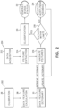
- an acoustic emission monitoring system 100 for measurement of acoustic emission signals emitted by semiconductor devices and for the identification of operational states of the monitored semiconductor devices, including identification of possible defects in the semiconductor device, based thereon.
- Semiconductor device 102 operates at a voltage of less than or equal to 220 V and preferably a power of less than or equal to 1 kW. Semiconductor device 102 may operate at a current in the range of 1mA - 1A. It is appreciated that semiconductor device 102 is thus preferably a relatively low power device. In some embodiments of the present invention, semiconductor device may be a microelectronic device. Semiconductor device 102 may also function in cooperation with, for example as controllers of, higher power electronics.
- a system such as acoustic monitoring system 100 to monitor semiconductor devices is based on the phenomenon of the generation of measurable acoustic emission signals 104 by such devices.
- These acoustic emission signals 104 have been found to arise from the semiconductor device itself, such that the semiconductor device is the source of the acoustic emission and the acoustic emission is originally created thereby.
- acoustic emission signals by the relatively low-power semiconductor devices in accordance with the present invention is believed by the present inventors to be due to electrical current causing charge-lattice interactions as a result of scattering of charges or due to electromagnetic forces, leading to atomic motion and hence the generation of measurable acoustic emission.
- charge-lattice interactions For example, in the case of a floating gate MOSFET transistor, the tunneling of electrons into the floating gate is accompanied by charge-lattice interactions, which charge-lattice interactions are believed to be a source of acoustic emission.
- the present inventors have found the acoustic emission signals to be influenced by electrical, thermal and/or mechanical stresses, including electrical failure, to which the semiconductor device may be subject.
- changes in the acoustic emission signals of the semiconductor device may be used to identify the presence of influential thermal, mechanical and or electrical stresses, which stresses may cause defects in the monitored device.
- the measured acoustic emission signals thus may be used to identify a state of the monitored device, such as on or off, identify internal device processes, such as read or write operation in a flash memory or the working mode of a micro-CPU, and to predict and/or diagnose malfunctions and deterioration of the device, as is further detailed henceforth. Such diagnosis may be valuable for monitoring and defect detection in expensive and/or mission critical electronic equipment and/or computational semiconductor devices.
- changes in the acoustic emission signals generated by an semiconductor device may be used to identify possible security breaches in control of the device, due for example to hacking or other malicious activities directed against the device via computerized controls thereof.
- the acoustic emission 104 emitted by semiconductor device 102 is preferably sensed by at least one acoustic measurement module, here embodied, by way of example, as an acoustic emission sensor 106.
- Acoustic emission sensor 106 preferably directly senses emission from device 102, which emission is generated by device 102 itself.
- Acoustic emission sensor 106 may be any type of acoustic emission sensor suitable for measuring acoustic emission, types of which are well known in the art and various examples of which are provided henceforth.
- acoustic emission sensor 106 may be one or more physically contacting or non-contacting sensor.
- the use of multiple acoustic emission sensors may be advantageous by enabling cross-correlation between the measured signals to allow cancelling out of environmental noise.
- acoustic emission sensor 106 may be incorporated within semiconductor device 102, for example, as a component installed on the PCB of device 102.
- At least one acoustic emission sensor 106 is preferably operative to sense acoustic emission emitted by at least one semiconductor device 102 and to output at least one acoustic emission signal corresponding thereto.
- Acoustic emission sensor 106 is preferably operative to sense acoustic emissions over at least one acoustic frequency range, which frequency range may comprise ultrasonic and/or sonic frequencies from several Hz to the GHz range.
- System 100 may optionally also include at least one additional sensor 107 for sensing at least one other parameter associated with semiconductor device 102, in addition to the sensing of acoustic emission by acoustic emission sensor 106.
- additional sensor 107 may sense one or more of electromagnetic emission, temperature, magnetic field strength and direction of device 102.
- System 100 further includes a signal processing unit 108 for receiving the at least one acoustic emission signal output by acoustic emission sensor 106 and analyzing the measured acoustic emission.
- Signal processing unit 108 provides an output 109 based on results of the analyzing performed thereby, which output is indicative at least of an operational state of device 102.
- the analyzing performed by signal processing unit 108 may include comparing the measured acoustic emission signal to at least one predetermined acoustic emission signal. Such comparing may be carried out in the time and/or frequency domain. Upon detection of deviation of the measured acoustic emission signal from the predetermined acoustic emission signal, signal processing unit 108 may provide an output indicative of such deviation.
- the predetermined acoustic emission signal and corresponding deviation therefrom may be one or more of an experimentally determined threshold signal associated with a given device, exceedance of which is indicative of a defect or of potential malfunction of the device; a historical emission signal or set of signals associated with a given device, deviation from which by a given statistical measure is indicative of a defect or potential malfunction of the device; and a collection of historical emission signals or set of signals from corresponding although not necessarily identical electronic devices, which electronic devices may be semiconductor devices, deviation from which by a given statistical measure is indicative of a defect or potential malfunction of the device.
- Such corresponding devices may share at least one common electrical feature with monitored device 102.
- signal processing unit 108 may include machine learning functionality.
- Machine learning functionality may be particularly useful in identifying when semiconductor device 102 or additional devices cooperating with semiconductor device 102 are affected by hacking or other malicious activities.
- the acoustic emission may deviate with respect to baseline acoustic emission patterns established during regular non-interfered operation of semiconductor device 102 or of other similar corresponding semiconductor devices sharing at least one electrical characteristic with semiconductor device 102.
- Machine learning algorithms as described henceforth may be used to detect such deviations and identify security breaches based thereon.
- Machine learning functionality included in signal processing unit 108 may be operative, by way of example, to perform machine learning on features of historical training data, the features being associated with corresponding operational states of devices from which the historical training data was obtained, and hence to classify an operating state of semiconductor device 102 based on correlations between features of the historical data and features of the measured acoustic emission signal of semiconductor device 102.
- the machine learning functionality of signal processing unit 108 may include any type of machine learning-based data mapping, processing and classification, including, by way of example only, statistic classifiers and self-learning neural networks. Further details concerning the various possible modes of operation of signal processing unit 108 are provided with reference to Fig. 2 .
- analysis of the measured acoustic emission may be used to classify an operating state of semiconductor device 102.
- analyzed features of the measured acoustic emission may be indicative of the electronic device being subject to stresses and/or failures, including electrical, thermal, and mechanical stresses, and hence be useful in diagnosis of defects and prognosis of impending malfunction of the device.
- signal processing unit 108 preferably receives an output from additional sensors 107, which output is indicative of those parameters sensed by sensors 107.
- Signal processing unit 108 may compare the output from additional sensors 107 to the measured acoustic emission signal provided by acoustic emission sensor 106, in order to derive possible correlations therebetween.
- the output 109 of signal processing unit 108 may be received by an alert unit 110, for alerting a user in at least near real time of the operating state of semiconductor device 102.
- alert unit 110 may provide a human sensible output alarm indication including at least a prediction of failure or time to failure of device 102 where relevant.
- alert unit 110 may be communicatively coupled to a feedback control unit 112, operative to provide automatic feedback control to semiconductor device 102, based on the nature of the operating state identified, including the potential malfunction or defect detected.
- feedback control unit 112 may modify or switch off the power supply to device 102.
- feedback control unit 112 may incorporate functionality for scheduling at least one repair or maintenance related operation on the device 102 based on the human sensible output alarm indication provided by alert unit 110.
- acoustic emission sensor 106 and additional optional sensors 107 are preferably included in a dedicated device package located proximal to device 102 being monitored, this is not necessarily the case for other components of system 100.
- signal processing unit 108, alert unit 110 and feedback control unit 112 may be included in a device package or may be part of a cloud service.
- signal processing unit 108 may include the functionality of alert unit 110
- alert unit 110 may include the functionality of feedback control unit 112 or acoustic emission sensor 106 may be combined with additional sensor modules 107.
- feedback control unit 112 may be obviated, for example in the case of a user of device 102 making manual rather than using automatic adjustments thereto upon receiving an alert from alert unit 110.
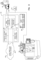
- Fig. 2 is a simplified flow chart illustrating signal acquisition and processing functionality of a system of the type shown in Fig. 1 . Particularly preferably, Fig. 2 illustrates signal processing functionality of a signal processing unit of system 100, such as signal processing unit 108.
- the signal processing functionality includes steps for calibration of a given semiconductor device under test (DUT), as illustrated in a first calibration column 202, as well as steps for actual measurement of the DUT, as illustrated in a second measurement column 204.
- DUT semiconductor device under test
- First calibration step 206 preferably involves the measurement of acoustic emission and calibration thereof in a variety of operational states of the DUT, including, by way of example, one or more of a non-powered state, an idle state, an active state, an electrically stressed state, a mechanically stressed state and a heated or cooled state.
- Such calibration may be used to establish a baseline acoustic emission signal, corresponding to normal operation of the DUT, which normal operation may be healthy rather than faulty operation or legitimate rather than illegitimate operation.
- First calibration step 206 may involve the measurement and calibration of acoustic emissions from the DUT itself, or from a population of similar electronic devices resembling but not necessarily identical to the DUT, using a crowd-sourcing approach.
- members of a population of electronic devices used for calibration measurements may be selected based on having at least one electrical characteristic in common with the DUT such as, by way of example, semiconductor devices having similar power consumption in similar operational states.
- the population of electronic devices based on which a given DUT may be calibrated may or may not include the DUT itself.
- the calibrated output for the various operational states of the DUT is preferably used to establish emission patterns or features associated with various DUT conditions, as seen at a second calculation step 208.
- emission features may be thresholds based on one or both of time domain and frequency domain spectral features of acoustic emission of the DUT in the various calibrated operational states thereof.
- emission features may additionally or alternatively be machine-learning based data trends or models. These emission features may be used to build up a dictionary of data features, as seen at third compilation step 210.
- the emission features derived at second calculation step 208 may be discrete acoustic signal thresholds corresponding to respective operational states of the DUT. These discrete thresholds may be unique to the particular DUT or may be standard thresholds found to be applicable to a range of similar semiconductor devices.
- the emission features derived at second step 208 may correspond to models of acoustic emission signals statistically correlated to respective operational states of the DUT, which models may be based on historical measurements of the acoustic emission signal over time and between various operating conditions of the DUT.
- the dictionary compiled at third step 210 may comprise or be augmented by data patterns identified based on statistical models of acoustic emission signals gleaned from historical measurements of acoustic emission signals of electronic devices sharing electrical characteristics with the DUT but not necessarily being identical thereto, based on a crowd-sourcing approach.
- the incorporation of data patterns based on related electronic devices in the emission patterns dictionary at third step 210 allows the compilation of a richer, more widely applicable dictionary having a higher confidence level associated therewith.
- first - third steps 206 - 210 shown in calibration column 202 are not necessarily carried out by signal processing unit 108. Depending on the particular thresholds applied, first - third steps 206 - 210 may be carried out by external, additional signal collection and processing modules and the emission pattern dictionary compiled at third step 210 stored at signal processing unit 108 or at a server.
- acoustic emission data generated by the DUT is received at a fourth step 212.
- acoustic emission data may be acquired by acoustic emission sensor 106 and received therefrom by signal processing unit 108.
- Feature extraction may include extraction of physical features of the acoustic emission, such as total acoustic emission energy, acoustic energy within defined time frames, acoustic energy within defined frequency bins and fluctuations in acoustic energy.
- Feature extraction may also include extraction of statistical features of the acoustic emission, including statistical moments and correlations and cumulants of acoustic signal, signal entropy and signal noise, as well as extraction of signal integrity features such as signal span and stationarity.
- Extracted features may be within predefined or machine-learned limits, allowing classification of the state of the DUT, as seen at an eighth step 220, leading to generation of a device status at a ninth step 222.
- the status may indicate deterioration of the DUT and predict impending failure prior to the occurrence of operational failure. Furthermore, the status may indicate the particular nature of the operational failure likely to occur.
- extracted features may deviate from the pre-defined or machine-learned baseline signals, indicating anomalous operation of the DUT as seen at a tenth step 224. Identification of malfunction of the DUT may result in the generation of a malfunction alert and/or feedback to the DUT, for example by way of alert unit 110 and feedback control unit 112 respectively.
- an output may be generated by alert unit 110 comprising a prediction of impending failure of the DUT based on similarities between patterns of change over time of the present measured acoustic emission signal and patterns of change over time of historical acoustic emission signals.
- z z 1 , z 2 , ... , z N
- z i p i ⁇ ⁇ i / ⁇ i
- ⁇ i mean of parameter p i under similar operating conditions in the same or similar device.
- z p ⁇ ⁇ T ⁇ ⁇ 1 p ⁇ ⁇
- ⁇ is a mean of parameter vector p known from historical data
- ⁇ is a covariance matrix calculated from historical data as well.
- the output of the system is expected time-to-failure (T ttf ).
- T rrf f z C
- C represents parameters of the learning system calculated from historical data on the same or similar devices.
- Acoustic emission signals 312 output by acoustic emission sensing module 310 are preferably provided to a signal processing subsystem 314 forming a part of an acoustic emission monitoring system 316.
- the analyzing performed by signal processing subsystem 314 may include application of an algorithm for extracting features of acoustic emission signals 312, in accordance with the various functionalities described hereinabove with reference to Fig. 2 .
- Data feature dictionary 322 may include predefined thresholds or data patterns derived based on past operation of micro-CPU 304. Additionally or alternatively, data feature dictionary 322 may be dynamically compiled based on crowd-sourcing of acoustic emission data patterns from a population of electronic components sharing electronic characteristics with micro-CPU 304.
- Such unusual acoustic emission spectra may indicate a possible security breach in the control and/or operation of motor 300 cooperating with and controlled by controller 302, of which controller 302 micro-CPU 304 forms a part.
- the acoustic emission signature of micro-CPU 304 thus may be used to evaluate whether micro-CPU 304 is operating in accordance with normal operating patterns or abnormal operating patterns, which abnormal operating patterns may be due to malicious interference in the operation of the motor 300 to which the micro-CPU 304 is connected.
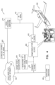
- an aircraft 400 may include electronic circuitry 402.
- Electronic circuitry 402 may include a variety of semiconductor components 404, including low-power semiconductor components, integrated circuits and PCBs on which a plurality of semiconductor components are mounted.
- semiconductor components 404 may be one or more of a CPU, microcontroller or memory chip or may be one or more PCBs on which one or more of such semiconductor components are mounted.
- electronic circuitry 402 is illustrated herein in a highly simplified form and may include a far greater and more complex arrangement of electronic components and PCBs therefore, as is well known in the art.
- Semiconductor components 404 may be operative to provide power, control or other functionalities to aircraft 400.
- An acoustic emission sensing module 410 is preferably coupled to at least one of semiconductor components 404.
- Acoustic emission sensing module 410 preferably comprises at least one acoustic emission sensor for sensing acoustic emission generated by at least one semiconductor component 404.
- Acoustic emission sensing module 410 may be directly mounted on semiconductor component 404, such that the at least one acoustic emission sensor is physically contacting the semiconductor component 404. Additionally or alternatively, acoustic emission sensing module 410 may be spatially separated from the semiconductor component 404, such that the acoustic emission sensor is not in physical contact therewith. It is appreciated that semiconductor component 404 and acoustic emission sensing module 410 correspond to a preferred embodiment of semiconductor device 102 and acoustic emission sensor 106 of Fig. 1 .
- Acoustic emission generated by semiconductor component 404 are preferably but not necessarily continuously sensed by acoustic emission sensing module 410.
- Acoustic emission sensing module 410 preferably outputs acoustic emission signals 412 corresponding to the acoustic emission spectra generated by electronic component 404.
- Acoustic emission signals 412 are preferably but not necessarily output by acoustic emission sensing module 410 in real time or near real time.
- Acoustic emission signals 412 output by acoustic emission sensing module 410 are preferably provided to a signal processing subsystem 414 forming a part of an acoustic emission monitoring system 416.
- Signal processing subsystem 414 may comprise computing functionality for analyzing the acoustic emission signals 412. The analyzing performed by signal processing subsystem 414 may include application of an algorithm for extracting features of acoustic emission signals 412, in accordance with the various functionalities described hereinabove with reference to Fig. 2 .
- Acoustic emission monitoring system 416 may optionally include other sensors, in addition to acoustic emission sensing module 410, in order to sense other parameters associated with electronic circuitry 402.
- other sensed parameters associated with electronic circuitry 402 may include temperature, electromagnetic radiation, magnetic field strength and humidity.
- an additional signal output representative of such parameters is preferably provided to signal processing subsystem 414 in addition to acoustic emission signals 412.
- Signal processing subsystem 414 is preferably operative to extract features of such additional signals.
- system 416 includes additional parameter sensors for sensing additional parameters associated with electronic component 404
- extracted features of such additional parameter signals may also be analyzed at server 420 in order to ascertain possible correlations between features of the acoustic emission signals 412 and features of the additional signals representing parameters other than acoustic emission.
- Classification 424 may be provided to a control subsystem 430, which control subsystem 430 is preferably in controlling communication with electronic circuitry 402 and/or semiconductor component 404.
- Control subsystem 430 is preferably operative to provide a feedback control 432 to electronic circuitry 402 and/or semiconductor component 404 responsive to the content of classification 424.
- Feedback control 432 is preferably, but not necessarily, automatic.
- the experimental data relates to the monitoring of measurable acoustic emission generated by semiconductor devices on a PCB, the monitoring of measurable acoustic emission generated by a PCB hosting semiconductor devices and the monitoring of measurable acoustic emission generated by a bare IC chip, not mounted on a PCB.
- the experiments presented hereinbelow were repeated several times on different ones of identical devices.
- semiconductor device 102 of Fig. 1 may be possible embodiments of semiconductor device 102 of Fig. 1 .
- similar ones of semiconductor devices described hereinbelow may collectively form a population of semiconductor devices providing historical or present acoustic emission measurements for use by signal processing unit 108 in analyzing acoustic emission signals from a semiconductor device.
- the experimental set-ups described hereinbelow may be combined with signal processing unit 108, real time alert unit 110 and feedback control unit 112 in order to allow identification and classification of operating states of the devices.
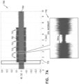
- FIG. 5 is a simplified block-diagram illustration showing an acoustic emission monitoring system, constructed and operative in accordance with a preferred embodiment of the present invention and used by the present inventors for measuring acoustic emission generated by one or more semiconductor components on a PCB.
- the acoustic emission sensors described as being employed in system 500 were ultrasound sensors, the monitored acoustic emission may additionally or alternatively be at frequencies lower than ultrasonic frequencies depending on the particular DUT, and appropriate acoustic emission sensors employed accordingly.
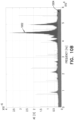
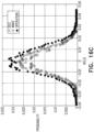
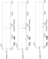
- peaks in the wakeup region 610 are characterized by a dominant frequency of approximately 166 KHz.
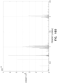
- the frequency domain acoustic emission power spectra generated by the flash memory as measured by first physically contacting acoustic emission sensor 502 are displayed in Figs. 6D , 6E and 6F , respectively displaying the acoustic emission intensity spectra for the flash memory in an idle, actively operating and wakeup state.
- the actively operating state of the flash corresponds to the storing of data in the flash.
- the data displayed corresponds to the raw data in the frequency domain following application of a 50 kHz high pass filter.
- a significantly higher acoustic emission intensity was measured in the wakeup and operative states, in comparison to the idle state, with the wakeup and operative states having acoustic emission intensity of the order of 10 -5 and 10 -4 V 2 in contrast to the idle state having acoustic emission intensity of the order of 10 -9 V 2 .
- the acoustic emission intensity spectra in the wakeup and operative states exhibit mutually difference acoustic emission features and signatures, allowing the acoustic emission spectra corresponding to the various operating states of the DUT to be readily identified and classified.
- an intensity peak is seen at approximately 166 KHz, corresponding to the dominant frequency of 166 kHz visible in Fig. 6C .
- the dominant frequency associated with the wakeup state of the flash memory is an additional feature of the acoustic emission that may be used in order to identify the flash memory operating state and detect anomalies thereof.
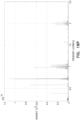
- the frequency domain acoustic emission intensity spectra generated by the flash memory as measured by second non-physically contacting microphone 506 are displayed in Figs. 6G , 6H and 6I , respectively displaying the acoustic emission intensity spectra for the flash memory in an idle, actively operating and wakeup state.
- the data displayed corresponds to the raw data in the frequency domain following application of a 50 kHz high pass filter.
- a significantly higher acoustic emission intensity was measured by microphone 506 in the wakeup and operative states, in comparison to the idle state. Furthermore, the acoustic emission intensity spectra in the wakeup and operative states exhibit mutually difference acoustic emission features and signatures, allowing the acoustic emission spectra corresponding to the various operating states of the DUT to be readily identified and classified. Additionally, with respect to the wakeup state spectrum displayed in Fig. 6I , an intensity peak is seen at approximately 166 KHz, corresponding to the dominant frequency of 166 kHz visible in Fig. 6C . The dominant frequency associated with the wakeup state of the flash memory is an additional feature of the acoustic emission that may be used in order to identify the flash memory operating state and detect anomalies thereof.
- Table 2 Statistical features of acoustic emission generated by flash memory in various operating states thereof, as measured by non-physically contacting microphone 506 Feature Idle state Wake-up state Active operating state Root Mean Square 0.0025 0.0048 0.043 Std. Deviation 0.0025 0.0048 0.043 Skewness -7.5x10 -10 2.5x10 -9 1.7x10 -11 Kurtosis 1.1x10 -10 3.2x10 -9 1x10 -9
- Probability distribution functions reflecting the statistical features of the various operating states of the flash memory, as measured by the sensor 502 and microphone 506, are displayed in Figs. 6J and 6K respectively.
- the probability distribution functions illustrate variations in statistical features of the spectra associated with the various operating states, allowing the use of higher order statistical moments as well as cumulants and other statistical measures for differentiating between and identifying various operating states of the device under test.
- the enhancement in electromagnetic radiation in the active state of the flash memory is believed to be due to electric currents and acceleration of charges within the device, which electric currents and accelerating charges interact with the host lattice to produce both electromagnetic and acoustic emission.
- the correlation between acoustic emission and electromagnetic radiation generated by the circuit during operation thereof may be used to identify operating states of the flash memory as well as to detect developing faults or failure of the flash memory based on features of both the acoustic and electromagnetic emission.
- the wakeup state acoustic emission spectra may be used for investigating the mechanism responsible for the generation of acoustic emission by the CPU.
- the rise and fall times of the acoustic emission during wakeup are significantly lower than the time taken for the PCB hosting the CPU to heat, according to calculations by the present inventors based on the thermal diffusivity of the CPU.
- the acoustic emission arises directly from charge-lattice interactions, such as electron-phonon scattering, leading to atomic motion of the host lattice rather than being due to indirect heating effects.
- a significantly higher acoustic emission power was measured in the wakeup and operative states, in comparison to the idle state, with the wakeup and operative states having acoustic emission intensity of the order of 10 -8 and 10 -7 V 2 in contrast to the idle state having acoustic emission intensity of the order of 10 -9 V 2 .
- the acoustic emission intensity spectra in the wakeup and operative states exhibit mutually difference acoustic emission features and signatures, allowing the acoustic emission spectra corresponding to the various operating states of the DUT to be readily identified and classified.
- a power peak is seen at approximately 166 KHz, corresponding to the dominant frequency of 166 kHz visible in Fig. 7C .
- the dominant frequency associated with the wakeup state of the CPU is an additional feature of the acoustic emission that may be used in order to identify the CPU operating state and detect anomalies thereof.
- the frequency domain acoustic emission power spectra generated by the CPU as measured by second non-physically contacting microphone 506 are displayed in Figs. 7G, 7H and 7I , respectively displaying the power spectra for the CPU in a wakeup, actively operating and idle state.
- the data displayed corresponds to the raw data in the frequency domain following application of a 50 kHz high pass filter.
- a significantly higher acoustic emission intensity was measured by microphone 506 in the wakeup and operative states, in comparison to the idle state. Furthermore, the acoustic emission intensity spectra in the wakeup and operative states exhibit mutually difference acoustic emission features and signatures, allowing the acoustic emission spectra corresponding to the various operating states of the DUT to be readily identified and classified. Additionally, with respect to the wakeup state spectrum displayed in Fig. 7G , a power peak is seen at approximately 166 KHz, corresponding to the dominant frequency of 166 kHz visible in Fig. 7C . The dominant frequency associated with the wakeup state of the CPU is an additional feature of the acoustic emission that may be used in order to identify the CPU operating state and detect anomalies thereof.
- the acoustic emission intensity as measured by physically contacting sensor 502 is greater than and different to that measured by non-physically contacting microphone 506. This is attributable to attenuation of the signal over the distance between the microphone 506 and the CPU, the acoustic transfer function that is orientation dependent with respect to the microphone and possible blocking of the acoustic emission by the sensor 502 due to sensor 502 resting on the surface of the CPU.
- Table 3 Statistical features of acoustic emission generated by CPU in various operating states thereof, as measured by the acoustic emission sensor 502 and non-contacting microphone 506, are tabulated in Tables 3 and 4 respectively.
- Table 3 Statistical features of acoustic emission generated by CPU in various operating states thereof, as measured by physically contacting acoustic emission sensor 502 Feature Idle state Wake-up state Active operating state Rms 3.5x10 -4 0.0041 0.0034 Std 3.5x10 -4 0.0041 0.0034 Skewness -3.5x10 -12 3x10 -9 4.8x10 -11 Kurtosis 1.1x10 -13 3.6x10 -9 3.5x10 -10
- Table 4 Statistical features of acoustic emission generated by CPU in various operating states thereof, as measured by non-physically contacting microphone 506 Feature Idle state Wake-up state Active operating state Rms 0.015 0.015 0.015 Std 0.015 0.015 0.015 Skewness -
- Probability distribution functions reflecting the statistical features of the various operating states of the CPU, as measured by the sensor 502 and microphone 506, are displayed in Figs. 7J and 7K respectively.
- the probability distribution functions illustrate variations in statistical features of the spectra associated with the various operating states, allowing the use of higher order statistical moments as well as cumulants and other statistical measures for differentiating between and identifying various operating states of the device under test and detecting faulty operation and incipient failure thereof.
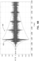
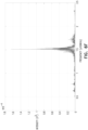
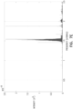
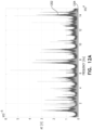
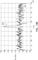
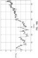
- Fig. 8 Acoustic emission energy as a function of frequency as measured by sensor 502 when the CPU was in an on state and an off state is presented in Fig. 8 .
- the acoustic emission energy during the off state of the CPU is represented by a first trace 802 and the acoustic emission energy during the on state of the CPU is represented by a second trace 804.
- the acoustic emission energy is seen to increase significantly during operation of the CPU in comparison to when the CPU is off.
- acoustic emission monitoring of low power devices such as a CPU on a commercial PCB may be useful for identifying operating states of the device and detecting development or presence of faults in the device based on deviations from predetermined or machine-learned features associated with the acoustic emission generated during various states of the device operation.
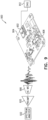
- FIG. 9 is a simplified block-diagram illustration showing an acoustic emission monitoring system, constructed and operative in accordance with another preferred embodiment of the present invention and used by the present inventors for measuring acoustic emission generated by one or more electronic components on a PCB, based on measurements made from the PCB itself.
- an acoustic emission monitoring system 900 preferably including at least one acoustic emission sensor, here embodied, by way of example, as a first acoustic emission sensor 902 preferably in physical contact with a DUT 904 and a second acoustic emission sensor 906, preferably not in physical contact with the DUT 904.
- first acoustic emission sensor 902 was a 150 kHz R15a ultrasonic sensor manufactured by MISTRAS of NJ, USA and second acoustic emission sensor 906 was an airborne ultrasonic microphone SPU410LR5H-QB manufactured by Knowles of IL, USA.
- First and second acoustic emission sensors 902 and 906 were each enclosed in a Faraday cage in order to shield them from EM radiation.
- DUT 904 is shown to be embodied as a PCB with at least one electronic component 908 mounted thereon, first acoustic emission sensor 902 preferably being in physical contact with surface of the PCB itself , rather than directly with the electronic component 908. It is appreciated, however, that sensor 902 may additionally or alternatively be in direct physical contact with at least one of electronic components 908, in addition to with the PCB board 904 itself.
- First acoustic emission sensor 902 is preferably connected to a data acquisition unit 912.
- Second acoustic emission sensor 906 is preferably connected to a preamplifier 920, which preamplifier 920 is preferably connected to a spectrum analyzer 922.
- data acquisition unit 912 was an NI-6351 data acquisition unit, manufactured by National Instruments of Texas, USA.
- Spectrum analyzer 922 was an E4402B spectrum analyzer, manufactured by Keysight of California, USA having a 1kHz resolution bandwidth.
- Preamplifier 920 was set to a gain of approximately 30 - 40 dB.
- the sampling frequency of DAQ 912 was set to 117 kHz.
- a low pass filter was connected upstream of preamplifier 920 for signal integrity testing.
- FIG. 9 An experimental set-up generally resembling that shown in Fig. 9 was used to monitor acoustic emission generated by a PCB-mounted microcontroller with an operating voltage of 3.3 V. Acoustic emission sensor 902 was located directly on top of the microcontroller, so as to be in direct physical contact therewith.
- Acoustic emission generated by the microcontroller was monitored during two operational states: a powered 'on' state and a non-powered 'off' state.
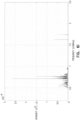
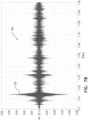
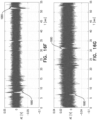
- Acoustic emission intensity as a function of time and frequency is displayed in Figs. 10A and 10B respectively, as measured by physically contacting sensor 902.
- measured acoustic emission in an 'on' state as represented by reference numeral 1002 is significantly enhanced in comparison to measured acoustic emission in an 'off' state, as represented by reference numeral 1004.
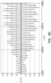
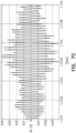
- acoustic emission as a function of frequency is displayed in Fig. 11 , as measured by microphone 906.
- the acoustic emission sensor within the microphone was approximately 1 cm distant from the microcontroller. Acoustic emission generated by the microcontroller was monitored during four operational states of the microcontroller: a non-powered 'off' state, a 'sleep' mode, an 'idle' mode and an active 'sampling' mode.
- acoustic emission when the device is in an off mode is represented by a first trace 1102
- acoustic emission when the device is in a sleep mode is represented by a second trace 1104
- acoustic emission when the device is in an idle mode is represented by a third trace 1106
- acoustic emission when the device is in an active sampling mode is represented by a forth trace 1108.
- acoustic emission when the microcontroller is in a powered state is significantly enhanced in comparison to acoustic emission when the device is in an off or sleep mode.
- acoustic emission energies are seen to differ between the idle and sleep modes, with the microcontroller generating significantly less acoustic emission in the sleep mode in comparison to the idle mode.
- measurable differences in acoustic emission may be detected and thus used to distinguish between on and off operational states of a microcontroller device mounted on a PCB. It is understood that the measured acoustic emission originates with the microcontroller device in both the on and off states thereof.
- the microcontroller is thus itself the source of the acoustic emission and is not simply a reflecting a portion of an acoustic signal received from an external source.
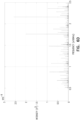
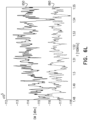
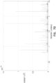
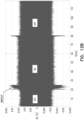
- Measured acoustic emission intensity as a function of frequency and time is displayed in Figs. 12A and 12B respectively. As seen both in the frequency domain ( Fig. 12A ) and time domain ( Fig. 12B ), measured acoustic emission during operation 1202 of the PCB is significantly enhanced in comparison to measured acoustic emission when the PCB is off 1204. An increase of 11% was found between the rms of the PCB 'on' state in comparison to that of the PCB 'off' state. Furthermore, an increase of 55% was found between the rms of the PCB 'wakeup', 'sleep' and 'shutdown' states in comparison to that of the PCB 'off' state. The statistical moments of the signal were also found to differ between the various states.
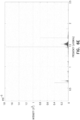
- Measured acoustic emission intensity as a function of time is displayed in Fig. 13 .
- Spikes in measured acoustic emission are seen in the time domain as well as changes in the statistical moments of the measured signal. These spikes may be attributable to temperature fluctuations or to voltage fluctuations caused by instability in the PCB grounding. The presence of these spikes support the hypothesis that electrical instability influences AE spectral energy, and thus changes in AE spectral energy and statistical features thereof may be used to detect or predict electrical failure.
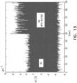
- Measured acoustic emission intensity as a function of time is displayed in Fig. 14 .
- measured acoustic emission during operation of the PCB under mechanical stress is enhanced in comparison to measured acoustic emission when mechanical stress is not applied.
- An increase of 10% was found between the rims of the PCB mechanically-stressed state in comparison to that of the PCB regular, non-stressed state.
- significant statistical differences were found between the signal distributions in the two states, including a difference in skewness of 38%.
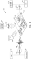
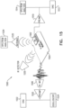
- an acoustic emission monitoring system 1500 preferably including at least one acoustic emission sensor, here embodied, by way of example, as a first acoustic emission sensor 1502 preferably in physical contact with a DUT 1504 and a second acoustic emission sensor 1506, preferably not in physical contact with the DUT 1504.
- first acoustic emission sensor 1502 was a R15a ultrasonic sensor manufactured by MISTRAS of NJ, USA and second acoustic emission sensor 1506 was an airborne ultrasonic microphone manufactured by Knowles of IL, USA.
- First and second acoustic emission sensors 1502 and 1506 were each provided enclosed in a Faraday cage in order to shield them from EM radiation.
- First and second preamplifiers 1510 and 1520 were each set to a gain of approximately 30 - 40 dB.
- the sampling frequency of first and second DAQs 1512 and 1522 was set to 500 kHz.
- Low pass filters were connected upstream of first and second preamplifiers 1510 and 1520 for signal integrity testing.
- Acoustic emission monitoring system 1500 may optionally additionally include an infra-red sensor 1530 for measuring the temperature of DUT 1504 and one or more antennas, here illustrated as a single antenna 1532, for measuring electromagnetic radiation generated by DUT 1504 and/or electronic components thereon.
- One or more antennas 1532 are preferably connected to a spectrum analyzer module 1534.
- system 1500 may include alternative components replacing the functionality of the illustrated components.
- a single acoustic emission sensor rather than two acoustic emission sensors may be included in system 1500
- first and second preamplifiers 1510, 1520 may be obviated
- the data acquisition units may be replaced by alternative sampling units
- oscilloscope 1524 may be replaced by a spectrum analyzer
- spectrum analyzer 1514 may be replaced by an oscilloscope having a fast fourier transform function
- additional or alternative frequency filters may be included and so forth.
- the acoustic emission sensors described as being employed in system 1500 were ultrasound sensors, the monitored acoustic emission may additionally or alternatively be at frequencies lower than ultrasonic frequencies depending on the particular DUT, and appropriate acoustic emission sensors employed accordingly.
- an acoustic emission monitoring system such as system 1500 may be incorporated within system 100, system 316 or system 416 described hereinabove. Particularly, system 1500 may form a part of a preferred embodiment of at least one acoustic sensor 1506 and signal processing unit 1508 in system 100 of Fig. 1 or of acoustic emission sensing modules 310 and 410 of Figs. 3 and 4 respectively.
- the signal from the spectrum analyzer corresponding to the acoustic emission measured by acoustic emission sensor 1502 is displayed in Fig. 16B .
- the resolution bandwidth of the spectrum analyzer was 1 kHz.
- enhance acoustic emission is visible for the active erase state, indicated by a first trace 1610, in comparison the acoustic emission in the idle state, indicated by a second trace 1620.
- a probability distribution function reflecting the statistical features of the various operating states of the flash, as measured by the sensor is displayed in Fig. 16C .
- the probability distribution function illustrates variations in statistical features of the spectra associated with the various operating states, allowing the use of higher order statistical moments as well as cumulants and other statistical measures for differentiating between and identifying various operating states of the device under test and detecting faulty operation and incipient failure thereof.
- the electromagnetic power generating during various operating states of the flash memory, as measured by passive antenna 1532, is displayed in Figs. 16D and 16E , showing power in the time and frequency domain respectively.
- the electromagnetic power generated by the flash memory in an active erase state as represented by a first trace 1650
- the electromagnetic power generated by the flash memory in an idle state as represented by a second trace 1660.
- An increase in electromagnetic power of approximately 8dBm is seen at a frequency range of about 200 kHz. This frequency range is consistent with the dominant frequency seen in the acoustic emission signature displayed in Fig. 16B , indicating a correlation between features of the electromagnetic emission and the acoustic emission.
- the electromagnetic power in the time domain is seen to be significantly enhanced during active operation in comparison to the idle state.
- the enhancement in electromagnetic radiation in the erase state of the flash memory is believed to be due to electron tunneling within the device, which tunneling generates electromagnetic radiation, in addition to the interaction of electrons with the host lattice producing both electromagnetic and acoustic emission.
- the correlation between acoustic emission and electromagnetic radiation generated by the flash memory during operation thereof may be used to identify operating states of the flash memory as well as to detect developing faults or failure of the flash memory based on features of both the acoustic and electromagnetic emission.
- Fig. 16F Acoustic emission measured by sensor 1502 during write operation by the flash is displayed in Fig. 16F and acoustic emission measured by sensor 1502 during read operation by the flash is displayed in Fig. 16G .
- the read and write state switching is accompanied by large fluctuations in acoustic emission.
- the two states may be differentiated by the longer duration of the write state as well as by the higher energy switching of the write state in comparison to the read state.
- the unstable signal seen during the read and write states may be attributable to the large drain-source current in these states. Since this current is oriented perpendicular to the direction of measurement, instabilities may be seen in the acoustic emission arising from the current.
- the frequency domain acoustic emission intensity spectra generated by the flash as measured by physically contacting sensor 1502 are displayed in Figs. 16H, 16I and 16J , respectively displaying the intensity spectra for the flash memory in wakeup, write and idle states.
- the frequency domain acoustic emission intensity spectra generated by the flash as measured by physically contacting sensor 1502 are displayed in Figs. 16K, 16L and 16M , respectively displaying the intensity spectra for the flash memory in wakeup, read and idle states.
- the various operating states are distinguished by different acoustic emission signatures having different statistical moments.
- the acoustic emission in the write mode is of higher amplitude than the acoustic emission in the read mode. This supports the hypothesis that the acoustic emission arises from the drain-source current, since the drain source current is lower in the read mode than in the write mode.
- Figs. 16N , 16O and 16P illustrate acoustic emission intensity in the frequency domain, generated by the flash memory and measured by microphone 1506 for the idle, operative write and wakeup states.
- the acoustic emission intensity spectra in the wakeup and operative write states exhibit mutually difference acoustic emission features and signatures, allowing the acoustic emission spectra corresponding to the various operating states of the flash to be readily identified and classified.
- the high acoustic energy at approximately 100 kHz and 200 kHz seen in Fig. 16O is associated with a line-bit write of approximately 5 microseconds, in accordance with values provided in the flash specification.
- the 100 kHz and 200 kHz peaks thus may be understood as attributable to drain source current in the flash during the write operation.
- Side bands at approximately 4 kHz are seen on either side of the 100 kHz and 200 kHz peaks, indicative of page write periods and associated with a page write time of approximately 250 microseconds, which duration is in keeping with values provided in the flash specification.
- a corresponding 200 kHz intensity peak was also found to be present in the acoustic emission sensor 1502 signal for the write operative state, although this is not seen in Figs. 16H - 16J due to the limited bandwidth displayed therein.
- Fig. 16Q illustrates acoustic emission arising from the flash memory in the case that the flash memory was programmed to work over an infinite loop of write/erase for a specific sector.
- measured acoustic emission was passed to a spectrum analyzer, where the spectrum analyzer was configured to measure at a central frequency of 200 kHz, with 10kHz span and resolution bandwidth of 1kHz. The measured signal was averaged over the span. It would be expected that the repetitive erase process would create oxide breakdown zones.
- the breakdown of oxide zones is a typical defect in flash memories and is responsible for data leakage. As seen in Fig. 16N , acoustic emission is seen to steadily increase over time. The increased acoustic emission may be due to breakdown of oxide zones resulting in reduced junction resistance and hence increased current and acoustic emission. These results indicate that changes to acoustic emission generated by the flash memory or other low-power semiconductor components may be monitored and use to detect electrical stress and electrical faults arising therefrom.
Landscapes
- Physics & Mathematics (AREA)
- General Physics & Mathematics (AREA)
- General Health & Medical Sciences (AREA)
- Pathology (AREA)
- Life Sciences & Earth Sciences (AREA)
- Chemical & Material Sciences (AREA)
- Analytical Chemistry (AREA)
- Biochemistry (AREA)
- Health & Medical Sciences (AREA)
- Immunology (AREA)
- Engineering & Computer Science (AREA)
- Signal Processing (AREA)
- Acoustics & Sound (AREA)
- Computer Hardware Design (AREA)
- Microelectronics & Electronic Packaging (AREA)
- General Engineering & Computer Science (AREA)
- Investigating Or Analyzing Materials By The Use Of Ultrasonic Waves (AREA)
Claims (7)
- System zum Überwachen und Identifizieren von Zuständen einer Halbleitervorrichtung (102, 508, 1504), wobei das System Folgendes umfasst:mindestens eine Halbleitervorrichtung, die mit einer Spannung kleiner oder gleich 220 V arbeitet, wobei die Halbleitervorrichtung entweder eine Mikrocontroller-Vorrichtung (508) oder eine Flash-Speichervorrichtung (1504) ist, die MOSFET-Transistoren mit schwebendem Gate umfasst;mindestens einen Schallsensor (106, 502, 506, 1502, 1506) zum Erfassen einer Schallemission (104), die durch die mindestens eine Halbleitervorrichtung emittiert wird, wobei der mindestens eine Schallsensor mindestens ein Signal ausgibt, das die Schallemission darstellt; undeine Signalverarbeitungseinheit (108) zum Empfangen des mindestens einen Signals, das die Schallemission darstellt, von dem mindestens einen Schallsensor und zum Analysieren des mindestens einen Signals, das die Schallemission darstellt,wobei die Signalverarbeitungseinheit auf der Grundlage der Analyse einen Ausgang (109) bereitstellt, wobei der Ausgang zumindest angibt, ob sich die mindestens eine Halbleitervorrichtung in Bezug auf einen regulären Betriebszustand der Halbleitervorrichtung in einem anomalen Betriebszustand befindet,wobei:
der Ausgang außerdem angibt, ob sich die Halbleitervorrichtung in einem aktiven Betriebszustand oder einem Ruhebetriebszustand befindet. - System nach Anspruch 1, wobei der reguläre Betriebszustand einen funktionsfähigen Zustand umfasst und der anomale Betriebszustand einen fehlerhaften Zustand umfasst.
- System nach Anspruch 1 oder Anspruch 2, wobei der Ausgang (109) eine Vorhersage eines bevorstehenden Fehlers der Halbleitervorrichtung (102) umfasst, wobei die Vorhersage auf Ähnlichkeiten zwischen Änderungsmustern im Zeitablauf des Schallemissionssignals (104) und Änderungsmustern im Zeitablauf von historischen Schallemissionssignalen, die vergangenen Fehlern der Halbleitervorrichtung zugeordnet sind, beruht.
- System nach einem der vorhergehenden Ansprüche, wobei die mindestens eine Halbleitervorrichtung (102) einen Feldeffekttransistor umfasst.
- Verfahren zum Überwachen und Identifizieren von Zuständen einer Halbleitervorrichtung (102, 508, 1504), die mit einer Spannung kleiner oder gleich 220 V arbeitet, wobei die Halbleitervorrichtung entweder eine Mikrocontroller-Vorrichtung oder eine Flash-Speichervorrichtung ist, die MOSFET-Transistoren mit schwebendem Gate umfasst, wobei das Verfahren Folgendes umfasst:Erfassen einer Schallemission (104), die durch die mindestens eine Halbleitervorrichtung emittiert wird;Analysieren der Schallemission; undBereitstellen eines Ausgangs (109) auf der Grundlage der Analyse, wobei der Ausgang zumindest angibt, ob sich die mindestens eine Halbleitervorrichtung in Bezug auf einen regulären Betriebszustand der Halbleitervorrichtung in einem anomalen Betriebszustand befindet,wobei:
der Ausgang außerdem angibt, ob sich die Halbleitervorrichtung in einem aktiven Betriebszustand oder einem Ruhebetriebszustand befindet. - Verfahren nach Anspruch 5, wobei der reguläre Betriebszustand einen funktionsfähigen Zustand umfasst und der anomale Betriebszustand einen fehlerhaften Zustand umfasst.
- Verfahren nach Anspruch 5 oder Anspruch 6, wobei das Bereitstellen des Ausgangs (109) das Bereitstellen einer Vorhersage eines bevorstehenden Fehlers der Halbleitervorrichtung (102) umfasst, wobei die Vorhersage auf Ähnlichkeiten zwischen Änderungsmustern im Zeitablauf des Schallemissionssignals (104) und Änderungsmustern im Zeitablauf von historischen Schallemissionssignalen, die vergangenen Fehlern der Halbleitervorrichtung zugeordnet sind, beruht.
Applications Claiming Priority (2)
| Application Number | Priority Date | Filing Date | Title |
|---|---|---|---|
| US201662406138P | 2016-10-10 | 2016-10-10 | |
| PCT/IL2017/051123 WO2018069922A2 (en) | 2016-10-10 | 2017-10-03 | Systems and methods for acoustic emission monitoring of semiconductor devices |
Publications (4)
| Publication Number | Publication Date |
|---|---|
| EP3500850A2 EP3500850A2 (de) | 2019-06-26 |
| EP3500850A4 EP3500850A4 (de) | 2019-09-18 |
| EP3500850B1 true EP3500850B1 (de) | 2025-07-09 |
| EP3500850C0 EP3500850C0 (de) | 2025-07-09 |
Family
ID=61905252
Family Applications (1)
| Application Number | Title | Priority Date | Filing Date |
|---|---|---|---|
| EP17860999.6A Active EP3500850B1 (de) | 2016-10-10 | 2017-10-03 | Systeme und verfahren zur schallemissionsüberwachung von halbleiterbauelementen |
Country Status (3)
| Country | Link |
|---|---|
| US (3) | US11493482B2 (de) |
| EP (1) | EP3500850B1 (de) |
| WO (1) | WO2018069922A2 (de) |
Families Citing this family (10)
| Publication number | Priority date | Publication date | Assignee | Title |
|---|---|---|---|---|
| US11493482B2 (en) | 2016-10-10 | 2022-11-08 | Augury Systems Ltd. | Systems and methods for acoustic emission monitoring of semiconductor devices |
| US11113168B2 (en) * | 2018-03-09 | 2021-09-07 | Toyota Motor Engineering & Manufacturing North America, Inc. | Distributed architecture for fault monitoring |
| EP3775962A4 (de) | 2018-04-09 | 2022-01-05 | Well Checked Systems International LLC | System und verfahren zum maschinenlernen von prädiktiver wartung durch hördetektion auf erdgasverdichtern |
| WO2019220609A1 (ja) | 2018-05-18 | 2019-11-21 | 日本電気株式会社 | 異常検出装置、異常検出方法及びプログラム |
| US11579598B2 (en) * | 2019-10-17 | 2023-02-14 | Mitsubishi Electric Research Laboratories, Inc. | Manufacturing automation using acoustic separation neural network |
| US11688413B2 (en) * | 2019-12-19 | 2023-06-27 | Taiwan Semiconductor Manufacturing Co., Ltd. | Method and system for audio recognition of arcing during semiconductor process |
| CN115077679A (zh) * | 2021-03-15 | 2022-09-20 | 创意电子股份有限公司 | 测试系统、裂音监听装置及裂音监听方法 |
| TWI797579B (zh) * | 2021-03-15 | 2023-04-01 | 創意電子股份有限公司 | 測試系統、裂音監聽裝置及裂音監聽方法 |
| CN116609638A (zh) * | 2023-05-19 | 2023-08-18 | 成都海光微电子技术有限公司 | 芯片检测方法、系统及计算机可读存储介质 |
| CN119669883B (zh) * | 2025-02-20 | 2025-05-09 | 四川吉利学院 | 基于人工智能的半导体自动化检测方法及检测设备 |
Family Cites Families (16)
| Publication number | Priority date | Publication date | Assignee | Title |
|---|---|---|---|---|
| JPS55117255A (en) * | 1979-03-02 | 1980-09-09 | Chiyou Lsi Gijutsu Kenkyu Kumiai | Method of detecting fault of semiconductor device |
| DE4006152A1 (de) | 1990-02-27 | 1991-08-29 | Fraunhofer Ges Forschung | Mikrominiaturisierte pumpe |
| US20020194915A1 (en) * | 2001-05-30 | 2002-12-26 | Abdel-Malek Aiman Albert | System and method for conditioned based monitoring using acoustic diagnosis |
| US6685638B1 (en) | 2002-12-23 | 2004-02-03 | Codman & Shurtleff, Inc. | Acoustic monitoring system |
| US7379718B2 (en) | 2004-12-20 | 2008-05-27 | Marvell World Trade Ltd. | Method and apparatus to manage power consumption of a semiconductor device |
| US7248985B2 (en) * | 2005-03-31 | 2007-07-24 | Honeywell International Inc. | Acoustic signature testing for electronic, electromechanical, and mechanical equipment |
| US20100049343A1 (en) | 2008-08-25 | 2010-02-25 | International Business Machines Corporation | Non-intrusive acoustic monitoring for equipment diagnostic and fault reporting |
| US20100300683A1 (en) | 2009-05-28 | 2010-12-02 | Halliburton Energy Services, Inc. | Real Time Pump Monitoring |
| WO2011156080A1 (en) * | 2010-06-09 | 2011-12-15 | Siemens Corporation | Systems and methods for learning of normal sensor signatures, condition monitoring and diagnosis |
| US20140208850A1 (en) * | 2013-01-29 | 2014-07-31 | Geun-Woo Kim | Apparatus and method of detecting a defect of a semiconductor device |
| US9429247B2 (en) | 2013-03-13 | 2016-08-30 | Applied Materials, Inc. | Acoustically-monitored semiconductor substrate processing systems and methods |
| US9178908B2 (en) | 2013-03-15 | 2015-11-03 | Shape Security, Inc. | Protecting against the introduction of alien content |
| US10478937B2 (en) * | 2015-03-05 | 2019-11-19 | Applied Materials, Inc. | Acoustic emission monitoring and endpoint for chemical mechanical polishing |
| EP3141893B1 (de) * | 2015-09-08 | 2019-12-11 | Mitsubishi Electric R&D Centre Europe B.V. | System zur bestimmung, ob in einer schnittstelle eines halbleiterchips eine verschlechterung stattfindet |
| JP6140331B1 (ja) * | 2016-04-08 | 2017-05-31 | ファナック株式会社 | 主軸または主軸を駆動するモータの故障予知を学習する機械学習装置および機械学習方法、並びに、機械学習装置を備えた故障予知装置および故障予知システム |
| US11493482B2 (en) | 2016-10-10 | 2022-11-08 | Augury Systems Ltd. | Systems and methods for acoustic emission monitoring of semiconductor devices |
-
2017
- 2017-10-03 US US16/337,712 patent/US11493482B2/en active Active
- 2017-10-03 EP EP17860999.6A patent/EP3500850B1/de active Active
- 2017-10-03 WO PCT/IL2017/051123 patent/WO2018069922A2/en not_active Ceased
-
2022
- 2022-10-24 US US18/049,166 patent/US20230076885A1/en not_active Abandoned
-
2023
- 2023-05-04 US US18/312,440 patent/US11977053B2/en active Active
Non-Patent Citations (2)
| Title |
|---|
| KÄRKKÄINEN TOMMI: "OBSERVATIONS OF ACOUSTIC EMISSION IN POWER SEMICONDUCTORS", 19 December 2015 (2015-12-19), pages 1 - 45, XP055401928, ISBN: 978-952-2659-11-8, Retrieved from the Internet <URL:https://www.doria.fi/bitstream/handle/10024/117932/Tommi%20K%C3%A4rkk%C3%A4inen%20A4.pdf?sequence=2> [retrieved on 20170829] * |
| MULLER SEBASTIAN ET AL: "Acoustic emission for state-of-health determination in power modules", 2016 13TH INTERNATIONAL MULTI-CONFERENCE ON SYSTEMS, SIGNALS & DEVICES (SSD), IEEE, 21 March 2016 (2016-03-21), pages 468 - 471, XP032900419, DOI: 10.1109/SSD.2016.7473704 * |
Also Published As
| Publication number | Publication date |
|---|---|
| US11493482B2 (en) | 2022-11-08 |
| US11977053B2 (en) | 2024-05-07 |
| WO2018069922A2 (en) | 2018-04-19 |
| WO2018069922A3 (en) | 2018-05-24 |
| US20230273159A1 (en) | 2023-08-31 |
| EP3500850C0 (de) | 2025-07-09 |
| EP3500850A4 (de) | 2019-09-18 |
| US20230076885A1 (en) | 2023-03-09 |
| EP3500850A2 (de) | 2019-06-26 |
| US20200033297A1 (en) | 2020-01-30 |
Similar Documents
| Publication | Publication Date | Title |
|---|---|---|
| US20230076885A1 (en) | Systems and methods for acoustic emission monitoring of semiconductor devices | |
| US12040531B2 (en) | Electronics card insitu testing apparatus and method utilizing unintended RF emission features | |
| Jiang et al. | Online anomaly detection in DC/DC converters by statistical feature estimation using GPR and GA | |
| US20100332199A1 (en) | Noise reduction technique for monitoring electromagnetic signals | |
| WO2016054626A1 (en) | Detection of malicious software, firmware, ip cores and circuitry via unintended emissions | |
| Biswas et al. | An industrial study of system-level test | |
| CN108226772A (zh) | 用于开关装置的诊断设备 | |
| Spyronasios et al. | Wavelet analysis for the detection of parametric and catastrophic faults in mixed-signal circuits | |
| Zhu et al. | PDNPulse: Sensing PCB anomaly with the intrinsic power delivery network | |
| US20180027003A1 (en) | Using photonic emission to develop electromagnetic emission models | |
| US10060982B2 (en) | Detecting faults in motors and drives | |
| Wang et al. | Spatial correlated data monitoring in semiconductor manufacturing using gaussian process model | |
| JP3861736B2 (ja) | ガス絶縁機器の部分放電診断装置 | |
| US20070157056A1 (en) | Method and apparatus for detecting defects in integrated circuit die from stimulation of statistical outlier signatures | |
| US20140218065A1 (en) | Detecting early failures in printed wiring boards | |
| EP3308180A1 (de) | Verfahren und vorrichtung zur identifizierung von empfindlichen integrierten schaltungsteilen für ein zufälliges telegrafisches signal | |
| Baybutt et al. | Seeded fault testing and in-situ analysis of critical electronic components in ema power circuitry | |
| CN114236273A (zh) | 性能检测方法、装置和检测设备 | |
| Haga et al. | Anomaly-Based Hardware Trojan Detection in PCB Supply Chains Using One-Class SVM Analysis of Capacitance Sensor Data | |
| RU2604578C1 (ru) | Способ контроля технического состояния элементов высоковольтного оборудования | |
| US20240210465A1 (en) | Method for determining wear in an electronic unit, and test apparatus | |
| Vasan et al. | Health assessment of electronic systems | |
| Carta et al. | Non-Destructive Detection of Counterfeit Audio Amplifier Modules | |
| Kunze et al. | Artificial neural networks based age estimation of electronic devices | |
| Zhang et al. | Analog Circuits Test by Using Principal Component Analysis |
Legal Events
| Date | Code | Title | Description |
|---|---|---|---|
| STAA | Information on the status of an ep patent application or granted ep patent |
Free format text: STATUS: THE INTERNATIONAL PUBLICATION HAS BEEN MADE |
|
| PUAI | Public reference made under article 153(3) epc to a published international application that has entered the european phase |
Free format text: ORIGINAL CODE: 0009012 |
|
| STAA | Information on the status of an ep patent application or granted ep patent |
Free format text: STATUS: REQUEST FOR EXAMINATION WAS MADE |
|
| 17P | Request for examination filed |
Effective date: 20190322 |
|
| AK | Designated contracting states |
Kind code of ref document: A2 Designated state(s): AL AT BE BG CH CY CZ DE DK EE ES FI FR GB GR HR HU IE IS IT LI LT LU LV MC MK MT NL NO PL PT RO RS SE SI SK SM TR |
|
| AX | Request for extension of the european patent |
Extension state: BA ME |
|
| A4 | Supplementary search report drawn up and despatched |
Effective date: 20190820 |
|
| RIC1 | Information provided on ipc code assigned before grant |
Ipc: G01H 3/10 20060101ALI20190813BHEP Ipc: G01R 31/307 20060101ALI20190813BHEP Ipc: G01H 1/00 20060101ALI20190813BHEP Ipc: G01N 29/14 20060101ALI20190813BHEP Ipc: G01D 7/00 20060101ALI20190813BHEP Ipc: G01R 31/28 20060101ALI20190813BHEP Ipc: G01N 29/00 20060101AFI20190813BHEP |
|
| DAV | Request for validation of the european patent (deleted) | ||
| DAX | Request for extension of the european patent (deleted) | ||
| STAA | Information on the status of an ep patent application or granted ep patent |
Free format text: STATUS: EXAMINATION IS IN PROGRESS |
|
| 17Q | First examination report despatched |
Effective date: 20210223 |
|
| GRAP | Despatch of communication of intention to grant a patent |
Free format text: ORIGINAL CODE: EPIDOSNIGR1 |
|
| STAA | Information on the status of an ep patent application or granted ep patent |
Free format text: STATUS: GRANT OF PATENT IS INTENDED |
|
| INTG | Intention to grant announced |
Effective date: 20250205 |
|
| GRAS | Grant fee paid |
Free format text: ORIGINAL CODE: EPIDOSNIGR3 |
|
| GRAA | (expected) grant |
Free format text: ORIGINAL CODE: 0009210 |
|
| STAA | Information on the status of an ep patent application or granted ep patent |
Free format text: STATUS: THE PATENT HAS BEEN GRANTED |
|
| AK | Designated contracting states |
Kind code of ref document: B1 Designated state(s): AL AT BE BG CH CY CZ DE DK EE ES FI FR GB GR HR HU IE IS IT LI LT LU LV MC MK MT NL NO PL PT RO RS SE SI SK SM TR |
|
| REG | Reference to a national code |
Ref country code: GB Ref legal event code: FG4D |
|
| REG | Reference to a national code |
Ref country code: CH Ref legal event code: EP |
|
| REG | Reference to a national code |
Ref country code: IE Ref legal event code: FG4D |
|
| REG | Reference to a national code |
Ref country code: DE Ref legal event code: R096 Ref document number: 602017090508 Country of ref document: DE |
|
| U01 | Request for unitary effect filed |
Effective date: 20250730 |
|
| U07 | Unitary effect registered |
Designated state(s): AT BE BG DE DK EE FI FR IT LT LU LV MT NL PT RO SE SI Effective date: 20250808 |
|
| U20 | Renewal fee for the european patent with unitary effect paid |
Year of fee payment: 9 Effective date: 20251028 |
|
| PG25 | Lapsed in a contracting state [announced via postgrant information from national office to epo] |
Ref country code: IS Free format text: LAPSE BECAUSE OF FAILURE TO SUBMIT A TRANSLATION OF THE DESCRIPTION OR TO PAY THE FEE WITHIN THE PRESCRIBED TIME-LIMIT Effective date: 20251109 |
|
| PGFP | Annual fee paid to national office [announced via postgrant information from national office to epo] |
Ref country code: GB Payment date: 20251022 Year of fee payment: 9 |
|
| PG25 | Lapsed in a contracting state [announced via postgrant information from national office to epo] |
Ref country code: NO Free format text: LAPSE BECAUSE OF FAILURE TO SUBMIT A TRANSLATION OF THE DESCRIPTION OR TO PAY THE FEE WITHIN THE PRESCRIBED TIME-LIMIT Effective date: 20251009 |
|
| PG25 | Lapsed in a contracting state [announced via postgrant information from national office to epo] |
Ref country code: HR Free format text: LAPSE BECAUSE OF FAILURE TO SUBMIT A TRANSLATION OF THE DESCRIPTION OR TO PAY THE FEE WITHIN THE PRESCRIBED TIME-LIMIT Effective date: 20250709 |
|
| PG25 | Lapsed in a contracting state [announced via postgrant information from national office to epo] |
Ref country code: GR Free format text: LAPSE BECAUSE OF FAILURE TO SUBMIT A TRANSLATION OF THE DESCRIPTION OR TO PAY THE FEE WITHIN THE PRESCRIBED TIME-LIMIT Effective date: 20251010 |
|
| PG25 | Lapsed in a contracting state [announced via postgrant information from national office to epo] |
Ref country code: PL Free format text: LAPSE BECAUSE OF FAILURE TO SUBMIT A TRANSLATION OF THE DESCRIPTION OR TO PAY THE FEE WITHIN THE PRESCRIBED TIME-LIMIT Effective date: 20250709 |
|
| PG25 | Lapsed in a contracting state [announced via postgrant information from national office to epo] |
Ref country code: RS Free format text: LAPSE BECAUSE OF FAILURE TO SUBMIT A TRANSLATION OF THE DESCRIPTION OR TO PAY THE FEE WITHIN THE PRESCRIBED TIME-LIMIT Effective date: 20251009 |
|
| PG25 | Lapsed in a contracting state [announced via postgrant information from national office to epo] |
Ref country code: ES Free format text: LAPSE BECAUSE OF FAILURE TO SUBMIT A TRANSLATION OF THE DESCRIPTION OR TO PAY THE FEE WITHIN THE PRESCRIBED TIME-LIMIT Effective date: 20250709 |