EP3499657A1 - Widely tunable laser with cross-connected ring resonator - Google Patents
Widely tunable laser with cross-connected ring resonator Download PDFInfo
- Publication number
- EP3499657A1 EP3499657A1 EP17306757.0A EP17306757A EP3499657A1 EP 3499657 A1 EP3499657 A1 EP 3499657A1 EP 17306757 A EP17306757 A EP 17306757A EP 3499657 A1 EP3499657 A1 EP 3499657A1
- Authority
- EP
- European Patent Office
- Prior art keywords
- signal
- reflecting filter
- filter
- filtered
- reflecting
- Prior art date
- Legal status (The legal status is an assumption and is not a legal conclusion. Google has not performed a legal analysis and makes no representation as to the accuracy of the status listed.)
- Granted
Links
- 230000002457 bidirectional effect Effects 0.000 claims abstract description 23
- 230000003287 optical effect Effects 0.000 claims abstract description 15
- 239000000758 substrate Substances 0.000 claims description 8
- VYPSYNLAJGMNEJ-UHFFFAOYSA-N Silicium dioxide Chemical compound O=[Si]=O VYPSYNLAJGMNEJ-UHFFFAOYSA-N 0.000 claims description 6
- 239000000463 material Substances 0.000 claims description 6
- 229910052710 silicon Inorganic materials 0.000 claims description 6
- 239000010703 silicon Substances 0.000 claims description 6
- 229910052581 Si3N4 Inorganic materials 0.000 claims description 3
- 239000012212 insulator Substances 0.000 claims description 3
- 239000000377 silicon dioxide Substances 0.000 claims description 3
- HQVNEWCFYHHQES-UHFFFAOYSA-N silicon nitride Chemical compound N12[Si]34N5[Si]62N3[Si]51N64 HQVNEWCFYHHQES-UHFFFAOYSA-N 0.000 claims description 3
- 101000969780 Homo sapiens Metallophosphoesterase 1 Proteins 0.000 abstract description 14
- 102100021274 Metallophosphoesterase 1 Human genes 0.000 abstract description 14
- 102100024829 DNA polymerase delta catalytic subunit Human genes 0.000 abstract description 12
- 101000868333 Homo sapiens Cyclin-dependent kinase 1 Proteins 0.000 abstract description 12
- 101000909198 Homo sapiens DNA polymerase delta catalytic subunit Proteins 0.000 abstract description 12
- 101000632319 Homo sapiens Septin-7 Proteins 0.000 abstract description 9
- 102100027981 Septin-7 Human genes 0.000 abstract description 9
- 230000001629 suppression Effects 0.000 abstract description 4
- 230000008033 biological extinction Effects 0.000 description 5
- 238000001914 filtration Methods 0.000 description 2
- 229910001218 Gallium arsenide Inorganic materials 0.000 description 1
- 230000005540 biological transmission Effects 0.000 description 1
- 210000001520 comb Anatomy 0.000 description 1
- 230000008878 coupling Effects 0.000 description 1
- 238000010168 coupling process Methods 0.000 description 1
- 238000005859 coupling reaction Methods 0.000 description 1
- 230000001066 destructive effect Effects 0.000 description 1
- 230000000694 effects Effects 0.000 description 1
- 230000005693 optoelectronics Effects 0.000 description 1
- 230000001902 propagating effect Effects 0.000 description 1
- 230000003595 spectral effect Effects 0.000 description 1
Images

Classifications
-
- H—ELECTRICITY
- H01—ELECTRIC ELEMENTS
- H01S—DEVICES USING THE PROCESS OF LIGHT AMPLIFICATION BY STIMULATED EMISSION OF RADIATION [LASER] TO AMPLIFY OR GENERATE LIGHT; DEVICES USING STIMULATED EMISSION OF ELECTROMAGNETIC RADIATION IN WAVE RANGES OTHER THAN OPTICAL
- H01S5/00—Semiconductor lasers
- H01S5/06—Arrangements for controlling the laser output parameters, e.g. by operating on the active medium
- H01S5/0607—Arrangements for controlling the laser output parameters, e.g. by operating on the active medium by varying physical parameters other than the potential of the electrodes, e.g. by an electric or magnetic field, mechanical deformation, pressure, light, temperature
- H01S5/0612—Arrangements for controlling the laser output parameters, e.g. by operating on the active medium by varying physical parameters other than the potential of the electrodes, e.g. by an electric or magnetic field, mechanical deformation, pressure, light, temperature controlled by temperature
-
- H—ELECTRICITY
- H01—ELECTRIC ELEMENTS
- H01S—DEVICES USING THE PROCESS OF LIGHT AMPLIFICATION BY STIMULATED EMISSION OF RADIATION [LASER] TO AMPLIFY OR GENERATE LIGHT; DEVICES USING STIMULATED EMISSION OF ELECTROMAGNETIC RADIATION IN WAVE RANGES OTHER THAN OPTICAL
- H01S5/00—Semiconductor lasers
- H01S5/10—Construction or shape of the optical resonator, e.g. extended or external cavity, coupled cavities, bent-guide, varying width, thickness or composition of the active region
- H01S5/14—External cavity lasers
- H01S5/141—External cavity lasers using a wavelength selective device, e.g. a grating or etalon
- H01S5/142—External cavity lasers using a wavelength selective device, e.g. a grating or etalon which comprises an additional resonator
-
- H—ELECTRICITY
- H01—ELECTRIC ELEMENTS
- H01S—DEVICES USING THE PROCESS OF LIGHT AMPLIFICATION BY STIMULATED EMISSION OF RADIATION [LASER] TO AMPLIFY OR GENERATE LIGHT; DEVICES USING STIMULATED EMISSION OF ELECTROMAGNETIC RADIATION IN WAVE RANGES OTHER THAN OPTICAL
- H01S5/00—Semiconductor lasers
- H01S5/10—Construction or shape of the optical resonator, e.g. extended or external cavity, coupled cavities, bent-guide, varying width, thickness or composition of the active region
- H01S5/1028—Coupling to elements in the cavity, e.g. coupling to waveguides adjacent the active region, e.g. forward coupled [DFC] structures
- H01S5/1032—Coupling to elements comprising an optical axis that is not aligned with the optical axis of the active region
Definitions
- the present invention relates to a reflecting filter for widely tunable lasers and associated widely tunable laser.
- Widely tunable lasers require a large tuning range (>100 nm) and high Side-Mode Suppression Ratio (SMSR).
- SMSR Side-Mode Suppression Ratio
- Such a tunable laser is composed of a gain region and a filter, with a large free spectral range (>100 nm), a narrow linewidth ( ⁇ 0,5 nm) and high extinction ratio (defined as ratio between the transmission at the filter's center wavelength and that at any other wavelength out of the filter's bandwidth) over the tuning range.
- the losses of the filter are expected to be low and have low wavelength dependency over the tuning range.
- the present invention proposes a reflecting filter, for widely tunable laser, adapted to filter and reflect an incoming optical signal so as to select a predetermined wavelength ⁇ to solve the prior art drawbacks.
- a reflecting filter comprises:
- the reflecting filter is grown on a platform among III-V material platform, silicon on insulator platform, doped silica platform or silicon nitride platform.
- the present invention also proposes an associated widely tunable laser that comprises a partially reflecting mirror, a gain section and a reflecting filter as previously described
- the widely tunable laser further comprises the following technical features taken alone or in combination:
- a first embodiment of a reflecting filter 10 is schematically illustrated in Figure 1 .
- This reflecting filter 10 comprises:
- the bidirectional port 1 receives an incoming optical signal IS that is splitted in two main signals MS1 and MS2 by the first codirectional coupler CDC1.
- codirectional coupler we mean a directional coupler from which we use both signals propagating in the same direction in the coupling region of the coupler and obtained from an incoming signal.
- the first main signal MS1 is sent to the second codirectional coupler CDC2 that splits the first main signal MS1 in two sub-signals SS1 and SS2 that are linked to the first ring resonator RR1.
- the optical paths followed by sub-signals SS1, SS2 (which are usually materialized by optical waveguides) and the first ring resonator RR1 form a first ring loop reflector.
- the first ring resonator RR1 filters both sub-signals SS1 and SS2 at a predetermined wavelength ⁇ _RR1 and sends the filtered signals obtained FS1 RR1 and FS2 RR1 back into the second codirectional coupler CDC2 so that the second codirectional coupler CDC2 sends the filtered signals FS1 RR1 and FS2 RR1 back into the first codirectional coupler CDC1.
- the first codirectional coupler CDC1 sends a part of the filtered signals FS1 RR1 and FS2 RR1 into the output 2 of the reflecting filter 10 which forms a transmitted signal TS, and sends the other part into the bidirectional port 1 so that it exits from the reflecting filter by the same way that the incoming optical signal IS originated and forming a reflecting signal RS.
- the filtered signal FS1 RR1 corresponds to the sub-signal SS1 which has been filtered, at the predetermined wavelength ⁇ _RR1, by the first ring resonator RR1.
- the filtered signal FS2 RR1 corresponds to the sub-signal SS2 which has been filtered, at the predetermined wavelength ⁇ _RR1, by this same first ring resonator RR1.
- the second main signal MS2 is sent to the third codirectional coupler CDC3 that splits the second main signal MS2 in two sub-signals SS3 and SS4 that are linked to the second ring resonator RR2.
- the optical paths followed by sub-beams SB3, SB4 and the second ring resonator RR2 form a second ring loop reflector that filters, at another predetermined wavelength ⁇ _RR2, the sub-beams SB3, SB4 and sends back the filtered signals FS3 RR2 and FS4 RR2 obtained back into the second codirectional coupler CDC2.
- a part of the filtered signals FS3 RR2 and FS4 RR2 is then sent back into the bidirectional port 1 so in the direction from which the incoming optical signal IS originated and corresponds to a second portion of the reflected signal RS.
- the other part is sent into the output 2 and forms a second portion of the transmitted signal TS.
- the filtered signal FS3 RR2 corresponds to the sub-signal SS3 which has been filtered, at the predetermined wavelength ⁇ _RR2, by the second ring resonator RR2.
- the filtered signal FS4 RR2 corresponds to the sub-signal SS4 which has been filtered, at the predetermined wavelength ⁇ _RR2, by this same second ring resonator RR2.
- the reflected signal RS and the transmitted signal TS comprise the four filtered signals FS1 RR1 , FS2 RR1 , FS3 RR2 and FS4 RR2 in different proportion depending on the characteristics of the codirectional couplers CDC1, CDC2 and CDC3.
- Each ring loop reflector provides a comb of resonance peaks thanks to the ring resonator RR1 and RR2.
- the total reflection will have high values. Consequently a laser incorporating such a filter can achieve the threshold at a wavelength close to the maximum value of the total reflection.
- Figure 2 illustrates an embodiment of such a laser 40 incorporating the reflecting filter 10, a gain section 20 and a partially reflecting mirror 30.
- the filter's extinction ratio is not be sufficiently high to guarantee a high SMSR for the tunable laser.
- the filter's extinction ratio is not be sufficiently high to guarantee a high SMSR for the tunable laser.
- the splitting ratio of the first codirectional coupler CDC1 changes with a amount of more than 10% over a wide wavelength range (100 nm for instance), the two reflected lights ⁇ FS1 RR1 ; FS2 RR1 ⁇ and ⁇ FS3 RR2 , FS4 RR2 ⁇ coming from the passage through the two ring resonators RR1 and RR2 do not have the same amount of amplitude, leading to reduced extinction ratio of the reflecting filter 10, which in turn leads to degraded SMSR of the widely tunable laser 40.
- the basic idea is to use a cross-connected ring resonator configuration, which allows to achieve a better suppression of undesirable resonances over a wide wavelength range. Consequently a widely wavelength tunable laser comprising such a reflecting filter 100 will have a better SMSR.
- This new reflecting filter 100 comprises the same elements as the previous reflecting filter 10, which are:
- the bidirectional port 1 receives an incoming optical signal IS that is splitted in two main signals MS1 and MS2 by the first codirectional coupler CDC1.
- the second codirectional coupler CDC2 is adapted to receive the first main signal MS1 and to split the first main signal MS1 in a first and second sub-signals SS1 and SS2.
- the third codirectional coupler CDC3 is adapted to receive the second main signal MS2 and to split the second main signal MS2 in a third and fourth sub-signals SS3 and SS4.
- the difference between the first reflecting filter embodiment 10 and the new reflecting filter embodiment 100 lies in that:
- the reflected signal RS' and the transmitted signal TS' comprise the four filtered signals FS1' RR1, FS2' RR2 , FS3' RR1 and FS4' RR2 in different proportions depending on the characteristics of the codirectional couplers CDC1, CDC2 and CDC3.
- the reflecting filter 100 can be build on different platforms among III-V (InP, GaAs) material platforms, silicon on insulator platforms, doped silica platforms or silicon nitride platforms for example.
- III-V InP, GaAs
- Figure 4 illustrates a widely tunable laser embodiment 140 comprising a partially reflecting mirror 130, a gain section 120 and a reflecting filter 100 as previously described, wherein the laser cavity is formed by the partially reflecting mirror and the reflecting filter.
- the gain section 120 and the reflecting filter 100 are monolithically integrated on a same substrate or the same plateform.
- This substrate or platform can be in silicon and the gain section can be in III-V material for example.
- the partially reflecting mirror 130 is one of the following: a Bragg reflector with a Bragg grating, a loop reflector, a cleaved facet or an etched facet.
- the partially reflecting mirror 130 can also be monolithically integrated with the gain section 120 and the reflecting filter 100.
Landscapes
- Physics & Mathematics (AREA)
- Condensed Matter Physics & Semiconductors (AREA)
- General Physics & Mathematics (AREA)
- Electromagnetism (AREA)
- Optics & Photonics (AREA)
- Semiconductor Lasers (AREA)
- Lasers (AREA)
Abstract
- a bidirectional port (1);
- an output (2);
- a first, a second and a third codirectional couplers (CDC1, CDC2, CDC3); and
- a first and second ring resonator (RR1, RR2) adapted to filter optical signals at the predetermined wavelength λ;
wherein a incoming signal (IS) is filtered at predetermined wavelength λ by the ring resonators (RR1, RR2) and reflected, the ring resonators (RR1, RR2) being cross-connected so to achieve a better suppression of undesirable resonances over a wide wavelength range. Consequently a widely wavelength tunable laser comprising such a reflecting filter (100) will have a better side-mode suppression ratio - SMSR.
Description
- The present invention relates to a reflecting filter for widely tunable lasers and associated widely tunable laser.
- Widely tunable lasers require a large tuning range (>100 nm) and high Side-Mode Suppression Ratio (SMSR). Such a tunable laser is composed of a gain region and a filter, with a large free spectral range (>100 nm), a narrow linewidth (< 0,5 nm) and high extinction ratio (defined as ratio between the transmission at the filter's center wavelength and that at any other wavelength out of the filter's bandwidth) over the tuning range. Moreover the losses of the filter are expected to be low and have low wavelength dependency over the tuning range.
- Current widely tunable lasers comprise ring resonators adapted to filter and thus select a particular wavelength. However, none of these widely tunable lasers offers, over a wide wavelength range, a sufficiently high extinction ratio that would guarantee a high SMSR for the tunable laser.
- So there is a need for filters with a high extinction ratio over a wide wavelength range that would improve SMSR and improve the performance stability over the wavelength tuning range.
- The present invention proposes a reflecting filter, for widely tunable laser, adapted to filter and reflect an incoming optical signal so as to select a predetermined wavelength λ to solve the prior art drawbacks.
- In a first and general aspect, a reflecting filter comprises:
- a bidirectional port;
- an output;
- a first, a second and a third codirectional couplers; and
- a first and second ring resonator adapted to filter optical signals at the predetermined wavelength λ;
- the bidirectional port receives the incoming optical signal that is splitted in two main signals and by the first codirectional coupler; then
- the second codirectional coupler is adapted to receive the first main signal and to split the first main signal in a first and second sub-signals;
- the third codirectional coupler is adapted to receive the second main signal and to split the second main signal in a third and fourth sub-signals;
- the first sub-signal is linked to the first ring resonator to be filtered at the predetermined wavelength λ, and the filtered signal obtained is sent back into the third codirectional coupler in order to be sent back to the first codirectional coupler which splits it in two and sends one splitted signal to the output of the reflecting filter, forming a first portion of a transmitted signal, and the other splitted signal to the bidirectional port so it goes out of the reflecting filter, and forming a first portion of a reflected signal;
- the second sub-signal is linked to the second ring resonator to be filtered at the predetermined wavelength λ, and the filtered signal obtained is sent back into the third codirectional coupler in order to be sent back to the first codirectional coupler which splits it in two and sends one splitted signal to the output of the reflecting filter, forming a second portion of the transmitted signal, and the other splitted signal to the bidirectional port so it goes out of the reflecting filter, and forming a second portion of the reflected signal;
- the third sub-signal is linked to the first ring resonator to be filtered at the predetermined wavelength λ, and the filtered signal obtained is sent back into the second codirectional coupler in order to be sent back to the first codirectional coupler which splits it in two and sends one splitted signal to the output of the reflecting filter, forming a third portion of the transmitted signal, and the other splitted signal to the bidirectional port so it goes out of the reflecting filter, and forming a third portion of the reflected signal; and
- the fourth sub-signal is linked to the second ring resonator to be filtered at the predetermined wavelength λ, and the filtered signal obtained is sent back into the second codirectional coupler in order to be sent back to the first codirectional coupler which splits it in two and sends one splitted signal to the output of the reflecting filter, forming a fourth portion of the transmitted signal, and the other splitted signal to the bidirectional port so it goes out of the reflecting filter, and forming a fourth portion of the reflected signal.
- Advantageously, the reflecting filter is grown on a platform among III-V material platform, silicon on insulator platform, doped silica platform or silicon nitride platform.
- The present invention also proposes an associated widely tunable laser that comprises a partially reflecting mirror, a gain section and a reflecting filter as previously described
- Advantageously, the widely tunable laser further comprises the following technical features taken alone or in combination:
- the gain section and the reflecting filter are monolithically integrated on a same substrate;
- the substrate is in silicon and the gain section is in III-V material;
- the partially reflecting mirror is one of the following: a Bragg reflector with a Bragg grating, a loop reflector, a cleaved facet or an etched facet;
- the partially reflecting mirror is one monolithically integrated with the gain section and the reflecting filter on a same substrate
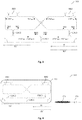
- Some embodiments of apparatus in accordance with embodiments of the present invention are now described, by way of example only, and with reference to the accompagnying drawings, in which :
-
Figure 1 schematically illustrates a first embodiment of a reflecting filter; -
Figure 2 schematically illustrates a widely tunable laser comprising a reflecting filter according to this first embodiment; -
Figure 3 schematically illustrates a new embodiment of a reflecting filter according to the invention; -
Figure 4 schematically illustrates a widely tunable laser comprising a reflecting filter according to this new embodiment. - A first embodiment of a reflecting
filter 10 is schematically illustrated inFigure 1 . - This reflecting
filter 10 comprises: - a
bidirectional port 1 and anoutput 2; - a first, a second and a third codirectional couplers CDC1, CDC2 and CDC3; and
- a first and a second ring resonators RR1 and RR2.
- The
bidirectional port 1 receives an incoming optical signal IS that is splitted in two main signals MS1 and MS2 by the first codirectional coupler CDC1. - By codirectional coupler, we mean a directional coupler from which we use both signals propagating in the same direction in the coupling region of the coupler and obtained from an incoming signal.
- The first main signal MS1 is sent to the second codirectional coupler CDC2 that splits the first main signal MS1 in two sub-signals SS1 and SS2 that are linked to the first ring resonator RR1.
- The optical paths followed by sub-signals SS1, SS2 (which are usually materialized by optical waveguides) and the first ring resonator RR1 form a first ring loop reflector. In fact, the first ring resonator RR1 filters both sub-signals SS1 and SS2 at a predetermined wavelength λ_RR1 and sends the filtered signals obtained FS1RR1 and FS2RR1 back into the second codirectional coupler CDC2 so that the second codirectional coupler CDC2 sends the filtered signals FS1RR1 and FS2RR1 back into the first codirectional coupler CDC1. Then, the first codirectional coupler CDC1 sends a part of the filtered signals FS1RR1 and FS2RR1 into the
output 2 of the reflectingfilter 10 which forms a transmitted signal TS, and sends the other part into thebidirectional port 1 so that it exits from the reflecting filter by the same way that the incoming optical signal IS originated and forming a reflecting signal RS. - The filtered signal FS1RR1 corresponds to the sub-signal SS1 which has been filtered, at the predetermined wavelength λ_RR1, by the first ring resonator RR1. The filtered signal FS2RR1 corresponds to the sub-signal SS2 which has been filtered, at the predetermined wavelength λ_RR1, by this same first ring resonator RR1.
- In the same way, the second main signal MS2 is sent to the third codirectional coupler CDC3 that splits the second main signal MS2 in two sub-signals SS3 and SS4 that are linked to the second ring resonator RR2.
- The optical paths followed by sub-beams SB3, SB4 and the second ring resonator RR2 form a second ring loop reflector that filters, at another predetermined wavelength λ_RR2, the sub-beams SB3, SB4 and sends back the filtered signals FS3RR2 and FS4RR2 obtained back into the second codirectional coupler CDC2. A part of the filtered signals FS3RR2 and FS4RR2 is then sent back into the
bidirectional port 1 so in the direction from which the incoming optical signal IS originated and corresponds to a second portion of the reflected signal RS. The other part is sent into theoutput 2 and forms a second portion of the transmitted signal TS. - The filtered signal FS3RR2 corresponds to the sub-signal SS3 which has been filtered, at the predetermined wavelength λ_RR2, by the second ring resonator RR2. The filtered signal FS4RR2 corresponds to the sub-signal SS4 which has been filtered, at the predetermined wavelength λ_RR2, by this same second ring resonator RR2.
- Thus the reflected signal RS and the transmitted signal TS comprise the four filtered signals FS1RR1, FS2RR1, FS3RR2 and FS4RR2 in different proportion depending on the characteristics of the codirectional couplers CDC1, CDC2 and CDC3.
- So it is as if the incoming signal IS had been reflected after being filtered, via the filtering and the sort of reflection of the sub-signals SS1, SS2, SS3, SS4, and corresponds after filtering and reflection to the reflected signal RS.
- Each ring loop reflector provides a comb of resonance peaks thanks to the ring resonator RR1 and RR2. When one resonance created by the first loop coincides in wavelength with one created by the second loop and when the two resonances are in phase, the total reflection will have high values. Consequently a laser incorporating such a filter can achieve the threshold at a wavelength close to the maximum value of the total reflection.
- To realise such a tunable laser, the ring resonators RR1 and RR2 must be tuned to that the first predetermined wavelength λ_RR1 is equal to the second predetermined wavelength λ_RR2 (λ_RR1 = λ_RR2). This can be done through thermal effects or electro-optical effects which allow, thus, the wavelength tuning of the laser.
-
Figure 2 illustrates an embodiment of such alaser 40 incorporating the reflectingfilter 10, a gain section 20 and a partially reflectingmirror 30. - However it appears that, with this first
tunable laser embodiment 40, the filter's extinction ratio is not be sufficiently high to guarantee a high SMSR for the tunable laser. In fact, when one resonance created by the first loop coincides in wavelength with one created by the second loop (so when λ_RR1 = λ_RR2) and when the two resonances are in phase, then the next coincidence between the two resonance combs is out of phase. Consequently, there is destructive interference at this coincidence. - However, the splitting ratio of the first codirectional coupler CDC1, as well as its combining ratio, changes with a amount of more than 10% over a wide wavelength range (100 nm for instance), the two reflected lights {FS1RR1 ; FS2RR1} and {FS3RR2, FS4RR2} coming from the passage through the two ring resonators RR1 and RR2 do not have the same amount of amplitude, leading to reduced extinction ratio of the reflecting
filter 10, which in turn leads to degraded SMSR of the widelytunable laser 40. - Consequently, an improvement of the first embodiment of the reflecting
filter 10 into a new reflectingfilter embodiment 100 is illustrated inFigure 3 . - In this new embodiment, the basic idea is to use a cross-connected ring resonator configuration, which allows to achieve a better suppression of undesirable resonances over a wide wavelength range. Consequently a widely wavelength tunable laser comprising such a reflecting
filter 100 will have a better SMSR. - This new reflecting
filter 100 comprises the same elements as the previous reflectingfilter 10, which are: - a
bidirectional port 1 and anoutput 2; - a first, a second and a third codirectional couplers CDC1, CDC2 and CDC3; and
- a first and a second ring resonators RR1 and RR2.
- The
bidirectional port 1 receives an incoming optical signal IS that is splitted in two main signals MS1 and MS2 by the first codirectional coupler CDC1. - The second codirectional coupler CDC2 is adapted to receive the first main signal MS1 and to split the first main signal MS1 in a first and second sub-signals SS1 and SS2. The third codirectional coupler CDC3 is adapted to receive the second main signal MS2 and to split the second main signal MS2 in a third and fourth sub-signals SS3 and SS4.
- The difference between the first reflecting
filter embodiment 10 and the new reflectingfilter embodiment 100 lies in that: - the first sub-signal SS1 is linked to the first ring resonator RR1 to be filtered at a predetermined wavelength λ_RR1, and the filtered signal FS1'RR1 obtained is sent back into the third codirectional coupler CDC3 in order to be sent back to the first codirectional coupler CDC1 which splits it in two and sends one splitted signal to the
output 2 of the reflectingfilter 100, forming a first portion of a transmitted signal TS', and the other splitted signal to thebidirectional port 1 so it goes out of the reflecting filter (100), and forming a first portion of a reflected signal RS'; - the second sub-signal SS2 is linked to the second ring resonator RR2 to be filtered at a predetermined wavelength λ_RR2, and the filtered signal FS2'RR2 obtained is sent back into the third codirectional coupler CDC3 in order to be sent back to the first codirectional coupler CDC1 which splits it in two and sends one splitted signal to the
output 2 of the reflectingfilter 100, forming a second portion of the transmitted signal TS', and the other splitted signal to thebidirectional port 1 so it goes out of the reflecting filter (100), and forming a second portion of the reflected signal RS'; - the third sub-signal SS3 is linked to the first ring resonator RR1 to be filtered at a predetermined wavelength λ_RR1, and the filtered signal FS3'RR1 obtained is sent bak into the second codirectional coupler CDC2 in order to be sent back to the first codirectional coupler CDC1 which splits it in two and sends one splitted signal to the
output 2 of the reflectingfilter 100, forming a third portion of the transmitted signal TS', and the other splitted signal to thebidirectional port 1 so it goes out of the reflecting filter (100), and forming a third portion of the reflected signal RS'; and - the fourth sub-signal SS4 is linked to the second ring resonator RR2 to be filtered at a predetermined wavelength λ_RR2, and the filtered signal FS4'RR2 obtained is sent back into the second codirectional coupler CDC2 in order to be sent back to the first codirectional coupler CDC1 which splits it in two and sends one splitted signal to the
output 2 of the reflectingfilter 100, forming a fourth portion of the transmitted signal TS', and the other splitted signal to thebidirectional port 1 so it goes out of the reflecting filter (100), and forming a fourth portion of the reflected signal RS'. - Thus the reflected signal RS' and the transmitted signal TS' comprise the four filtered signals FS1'RR1, FS2'RR2, FS3'RR1 and FS4'RR2 in different proportions depending on the characteristics of the codirectional couplers CDC1, CDC2 and CDC3.
- In order to be used in a widely tunable laser, the ring resonators RR1 and RR2 are advantageously tuned so that their resonating wavelengths which correspond to the predetermined wavelengths λ_RR1 and λ_RR2 are equal to a predetermined wavelength λ (λ_RR1 = λ_RR2 = λ), that corresponds to the wavelength desired in the widely tunable laser.
- Advantageouly, the reflecting
filter 100 can be build on different platforms among III-V (InP, GaAs) material platforms, silicon on insulator platforms, doped silica platforms or silicon nitride platforms for example. -
Figure 4 illustrates a widelytunable laser embodiment 140 comprising a partially reflectingmirror 130, again section 120 and a reflectingfilter 100 as previously described, wherein the laser cavity is formed by the partially reflecting mirror and the reflecting filter. - Advantageously, the
gain section 120 and the reflectingfilter 100 are monolithically integrated on a same substrate or the same plateform. This substrate or platform can be in silicon and the gain section can be in III-V material for example. - Advantageously, the partially reflecting
mirror 130 is one of the following: a Bragg reflector with a Bragg grating, a loop reflector, a cleaved facet or an etched facet. The partially reflectingmirror 130 can also be monolithically integrated with thegain section 120 and the reflectingfilter 100. - The description and drawings merely illustrate the principles of the invention. It will thus be appreciated that those skilled in the art will be able to devise various arrangements that, although not explicitly described or shown herein, embody the principles of the invention and are included within its spirit and scope. Furthermore, all examples recited herein are principally intended expressly to be only for pedagogical purposes to aid the reader in understanding the principles of the invention and the concepts contributed by the inventors to furthering the art, and are to be construed as being without limitation to such specifically recited examples and conditions. Moreover, all statements herein reciting principles, aspects, and embodiments of the invention, as well as specific examples thereof, are intended to encompass equivalents thereof.
Claims (7)
- A reflecting filter (100), for widely tunable laser, adapted to filter and reflect an incoming optical signal (IS) so as to select a predetermined wavelength λ, the reflecting filter (100) comprising:- a bidirectional port (1);- an output (2);- a first, a second and a third codirectional couplers (CDC1, CDC2, CDC3); and- a first and second ring resonator (RR1, RR2) adapted to filter optical signals at the predetermined wavelength λ;wherein- the bidirectional port (1) is adapted to receive the incoming optical signal (IS) that is splitted in two main signals (MS1) and (MS2) by the first codirectional coupler (CDC1); then- the second codirectional coupler (CDC2) is adapted to receive the first main signal (MS1) and to split the first main signal (MS1) in a first and second sub-signals (SS1, SS2);- the third codirectional coupler (CDC3) is adapted to receive the second main signal (MS2) and to split the second main signal (MS2) in a third and fourth sub-signals (SS3, SS4);- the first sub-signal (SS1) is linked to the first ring resonator (RR1) to be filtered at the predetermined wavelength λ, and the filtered signal (FS1'RR1) obtained is sent back into the third codirectional coupler (CDC3) in order to be sent back to the first codirectional coupler (CDC1) which splits it in two and sends one splitted signal to the output (2) of the reflecting filter (100), forming a first portion of a transmitted signal (TS'), and the other splitted signal to the bidirectional port (1) so it goes out of the reflecting filter (100), and forming a first portion of a reflected signal (RS');- the second sub-signal (SS2) is linked to the second ring resonator (RR2) to be filtered at the predetermined wavelength λ, and the filtered signal (FS2'RR2) obtained is sent back into the third codirectional coupler (CDC3) in order to be sent back to the first codirectional coupler (CDC1) which splits it in two and sends one splitted signal to the output (2) of the reflecting filter (100), forming a second portion of the transmitted signal (TS'), and the other splitted signal to the bidirectional port (1) so it goes out of the reflecting filter (100), and forming a second portion of the reflected signal (RS');- the third sub-signal (SS3) is linked to the first ring resonator (RR1) to be filtered at the predetermined wavelength λ, and the filtered signal (FS3'RR1) obtained is sent back into the second codirectional coupler (CDC2) in order to be sent back to the first codirectional coupler (CDC1) which splits it in two and sends one splitted signal to the output (2) of the reflecting filter (100), forming a third portion of the transmitted signal (TS'), and the other splitted signal to the bidirectional port (1) so it goes out of the reflecting filter (100), and forming a third portion of the reflected signal (RS'); and- the fourth sub-signal (SS4) is linked to the second ring resonator (RR2) to be filtered at the predetermined wavelength λ, and the filtered signal (FS4'RR2) obtained is sent back into the second codirectional coupler (CDC2) in order to be sent back to the first codirectional coupler (CDC1) which splits it in two and sends one splitted signal to the output (2) of the reflecting filter (100), forming a fourth portion of the transmitted signal (TS'), and the other splitted signal to the bidirectional port (1) so it goes out of the reflecting filter (100), and forming a fourth portion of the reflected signal (RS').
- The reflecting filter (100) according to claim 1 wherein the reflecting filter (100) is grown on a platform among III-V material platform, silicon on insulator platform, doped silica platform or silicon nitride platform.
- A widely tunable laser (140) comprising a partially reflecting mirror (130), a gain section (120) and a reflecting filter (100) as described in one of the claims 1 and 2, wherein the laser cavity is formed by the partially reflecting mirror (130) and the reflecting filter (100).
- The widely tunable laser (140) according to claim 3 wherein the gain section (120) and the reflecting filter (100) are monolithically integrated on a same substrate.
- The widely tunable laser (140) according to claim 4 wherein the substrate is in silicon and the gain section (120) is in III-V material.
- The widely tunable laser (140) according to one of the claims 3 to 5 wherein the partially reflecting mirror (130) is one of the following: a Bragg reflector with a Bragg grating, a loop reflector, a cleaved facet or an etched facet.
- The widely tunable laser (140) according to one of the claims 3 to 6 wherein the partially reflecting mirror (130) is one monolithically integrated with the gain section (120) and the reflecting filter (100) on a same substrate.
Priority Applications (2)
| Application Number | Priority Date | Filing Date | Title |
|---|---|---|---|
| EP17306757.0A EP3499657B1 (en) | 2017-12-12 | 2017-12-12 | Widely tunable laser with cross-connected ring resonator |
| PCT/EP2018/083556 WO2019115300A1 (en) | 2017-12-12 | 2018-12-04 | Widely tunable laser with cross-connected ring resonator |
Applications Claiming Priority (1)
| Application Number | Priority Date | Filing Date | Title |
|---|---|---|---|
| EP17306757.0A EP3499657B1 (en) | 2017-12-12 | 2017-12-12 | Widely tunable laser with cross-connected ring resonator |
Publications (2)
| Publication Number | Publication Date |
|---|---|
| EP3499657A1 true EP3499657A1 (en) | 2019-06-19 |
| EP3499657B1 EP3499657B1 (en) | 2020-06-17 |
Family
ID=60673886
Family Applications (1)
| Application Number | Title | Priority Date | Filing Date |
|---|---|---|---|
| EP17306757.0A Active EP3499657B1 (en) | 2017-12-12 | 2017-12-12 | Widely tunable laser with cross-connected ring resonator |
Country Status (2)
| Country | Link |
|---|---|
| EP (1) | EP3499657B1 (en) |
| WO (1) | WO2019115300A1 (en) |
Citations (3)
| Publication number | Priority date | Publication date | Assignee | Title |
|---|---|---|---|---|
| US20140133511A1 (en) * | 2011-08-10 | 2014-05-15 | Fujitsu Limited | Semiconductor optical element |
| CN106785882A (en) * | 2016-11-30 | 2017-05-31 | 武汉光迅科技股份有限公司 | A kind of silicon substrate tunable external cavity laser of high power dual-port output |
| US9778493B1 (en) * | 2016-09-22 | 2017-10-03 | Oracle International Corporation | Dual-ring-modulated laser that uses push-push/pull-pull modulation |
-
2017
- 2017-12-12 EP EP17306757.0A patent/EP3499657B1/en active Active
-
2018
- 2018-12-04 WO PCT/EP2018/083556 patent/WO2019115300A1/en not_active Ceased
Patent Citations (3)
| Publication number | Priority date | Publication date | Assignee | Title |
|---|---|---|---|---|
| US20140133511A1 (en) * | 2011-08-10 | 2014-05-15 | Fujitsu Limited | Semiconductor optical element |
| US9778493B1 (en) * | 2016-09-22 | 2017-10-03 | Oracle International Corporation | Dual-ring-modulated laser that uses push-push/pull-pull modulation |
| CN106785882A (en) * | 2016-11-30 | 2017-05-31 | 武汉光迅科技股份有限公司 | A kind of silicon substrate tunable external cavity laser of high power dual-port output |
Also Published As
| Publication number | Publication date |
|---|---|
| WO2019115300A1 (en) | 2019-06-20 |
| EP3499657B1 (en) | 2020-06-17 |
Similar Documents
| Publication | Publication Date | Title |
|---|---|---|
| US9748726B1 (en) | Multiple-microresonator based laser | |
| US9356419B1 (en) | Temperature insensitive external cavity lasers on silicon | |
| US20200076153A1 (en) | Tunable laser with directional coupler | |
| US6970484B2 (en) | Laser tuning by spectrally dependent spatial filtering | |
| JP2957116B2 (en) | Tunable laser device | |
| US7149381B2 (en) | Optical filtering device and method | |
| US20090154505A1 (en) | Wavelength tunable laser diode using double coupled ring resonator | |
| US20230411929A1 (en) | Narrow linewidth semiconductor laser | |
| US11862924B2 (en) | Low noise lasers with resonator filters | |
| Xiang et al. | Widely tunable Si 3 N 4 triple-ring and quad-ring resonator laser reflectors and filters | |
| CN113644543A (en) | A wavelength-tunable semiconductor laser | |
| US12212120B2 (en) | Tunable Vernier effect laser emission device | |
| JP5001239B2 (en) | Semiconductor tunable laser | |
| US20160170286A1 (en) | Optical Device with Integrated Reflector(s) Comprising a Loop Reflector Integrating a Mach-Zehnder Interferometer | |
| WO2020145173A1 (en) | Tunable laser | |
| US6498799B1 (en) | Single-mode fiber ring laser | |
| US20230231356A1 (en) | Fabry-perot based multi resonant cavity tunable laser | |
| EP3499657B1 (en) | Widely tunable laser with cross-connected ring resonator | |
| EP2645496A1 (en) | A wavelength tunable semiconductor laser | |
| JP2004511914A (en) | Tunable single mode laser device | |
| Yoon et al. | Monolithically integrated tunable laser using double-ring resonators with a tilted multimode interference coupler | |
| Troppenz et al. | All-active InGaAsP/InP ring cavities for widespread functionalities in the wavelength domain | |
| US12197003B2 (en) | Optical filter and wavelength tunable laser element | |
| JPS63299291A (en) | Semiconductor laser | |
| JP7189431B2 (en) | Tunable laser |
Legal Events
| Date | Code | Title | Description |
|---|---|---|---|
| PUAI | Public reference made under article 153(3) epc to a published international application that has entered the european phase |
Free format text: ORIGINAL CODE: 0009012 |
|
| STAA | Information on the status of an ep patent application or granted ep patent |
Free format text: STATUS: THE APPLICATION HAS BEEN PUBLISHED |
|
| AK | Designated contracting states |
Kind code of ref document: A1 Designated state(s): AL AT BE BG CH CY CZ DE DK EE ES FI FR GB GR HR HU IE IS IT LI LT LU LV MC MK MT NL NO PL PT RO RS SE SI SK SM TR |
|
| AX | Request for extension of the european patent |
Extension state: BA ME |
|
| RAP1 | Party data changed (applicant data changed or rights of an application transferred) |
Owner name: NOKIA SOLUTIONS AND NETWORKS OY |
|
| STAA | Information on the status of an ep patent application or granted ep patent |
Free format text: STATUS: REQUEST FOR EXAMINATION WAS MADE |
|
| 17P | Request for examination filed |
Effective date: 20191209 |
|
| RBV | Designated contracting states (corrected) |
Designated state(s): AL AT BE BG CH CY CZ DE DK EE ES FI FR GB GR HR HU IE IS IT LI LT LU LV MC MK MT NL NO PL PT RO RS SE SI SK SM TR |
|
| GRAP | Despatch of communication of intention to grant a patent |
Free format text: ORIGINAL CODE: EPIDOSNIGR1 |
|
| STAA | Information on the status of an ep patent application or granted ep patent |
Free format text: STATUS: GRANT OF PATENT IS INTENDED |
|
| RIC1 | Information provided on ipc code assigned before grant |
Ipc: H01S 5/06 20060101ALN20200109BHEP Ipc: H01S 5/14 20060101AFI20200109BHEP Ipc: H01S 5/10 20060101ALN20200109BHEP |
|
| RIC1 | Information provided on ipc code assigned before grant |
Ipc: H01S 5/14 20060101AFI20200123BHEP Ipc: H01S 5/10 20060101ALN20200123BHEP Ipc: H01S 5/06 20060101ALN20200123BHEP |
|
| INTG | Intention to grant announced |
Effective date: 20200206 |
|
| GRAS | Grant fee paid |
Free format text: ORIGINAL CODE: EPIDOSNIGR3 |
|
| GRAA | (expected) grant |
Free format text: ORIGINAL CODE: 0009210 |
|
| STAA | Information on the status of an ep patent application or granted ep patent |
Free format text: STATUS: THE PATENT HAS BEEN GRANTED |
|
| AK | Designated contracting states |
Kind code of ref document: B1 Designated state(s): AL AT BE BG CH CY CZ DE DK EE ES FI FR GB GR HR HU IE IS IT LI LT LU LV MC MK MT NL NO PL PT RO RS SE SI SK SM TR |
|
| REG | Reference to a national code |
Ref country code: GB Ref legal event code: FG4D |
|
| REG | Reference to a national code |
Ref country code: CH Ref legal event code: EP |
|
| REG | Reference to a national code |
Ref country code: IE Ref legal event code: FG4D |
|
| REG | Reference to a national code |
Ref country code: DE Ref legal event code: R096 Ref document number: 602017018272 Country of ref document: DE |
|
| REG | Reference to a national code |
Ref country code: AT Ref legal event code: REF Ref document number: 1282492 Country of ref document: AT Kind code of ref document: T Effective date: 20200715 |
|
| PG25 | Lapsed in a contracting state [announced via postgrant information from national office to epo] |
Ref country code: FI Free format text: LAPSE BECAUSE OF FAILURE TO SUBMIT A TRANSLATION OF THE DESCRIPTION OR TO PAY THE FEE WITHIN THE PRESCRIBED TIME-LIMIT Effective date: 20200617 Ref country code: GR Free format text: LAPSE BECAUSE OF FAILURE TO SUBMIT A TRANSLATION OF THE DESCRIPTION OR TO PAY THE FEE WITHIN THE PRESCRIBED TIME-LIMIT Effective date: 20200918 Ref country code: NO Free format text: LAPSE BECAUSE OF FAILURE TO SUBMIT A TRANSLATION OF THE DESCRIPTION OR TO PAY THE FEE WITHIN THE PRESCRIBED TIME-LIMIT Effective date: 20200917 Ref country code: LT Free format text: LAPSE BECAUSE OF FAILURE TO SUBMIT A TRANSLATION OF THE DESCRIPTION OR TO PAY THE FEE WITHIN THE PRESCRIBED TIME-LIMIT Effective date: 20200617 Ref country code: SE Free format text: LAPSE BECAUSE OF FAILURE TO SUBMIT A TRANSLATION OF THE DESCRIPTION OR TO PAY THE FEE WITHIN THE PRESCRIBED TIME-LIMIT Effective date: 20200617 |
|
| REG | Reference to a national code |
Ref country code: LT Ref legal event code: MG4D |
|
| REG | Reference to a national code |
Ref country code: NL Ref legal event code: MP Effective date: 20200617 |
|
| PG25 | Lapsed in a contracting state [announced via postgrant information from national office to epo] |
Ref country code: BG Free format text: LAPSE BECAUSE OF FAILURE TO SUBMIT A TRANSLATION OF THE DESCRIPTION OR TO PAY THE FEE WITHIN THE PRESCRIBED TIME-LIMIT Effective date: 20200917 Ref country code: RS Free format text: LAPSE BECAUSE OF FAILURE TO SUBMIT A TRANSLATION OF THE DESCRIPTION OR TO PAY THE FEE WITHIN THE PRESCRIBED TIME-LIMIT Effective date: 20200617 Ref country code: LV Free format text: LAPSE BECAUSE OF FAILURE TO SUBMIT A TRANSLATION OF THE DESCRIPTION OR TO PAY THE FEE WITHIN THE PRESCRIBED TIME-LIMIT Effective date: 20200617 Ref country code: HR Free format text: LAPSE BECAUSE OF FAILURE TO SUBMIT A TRANSLATION OF THE DESCRIPTION OR TO PAY THE FEE WITHIN THE PRESCRIBED TIME-LIMIT Effective date: 20200617 |
|
| REG | Reference to a national code |
Ref country code: AT Ref legal event code: MK05 Ref document number: 1282492 Country of ref document: AT Kind code of ref document: T Effective date: 20200617 |
|
| PG25 | Lapsed in a contracting state [announced via postgrant information from national office to epo] |
Ref country code: AL Free format text: LAPSE BECAUSE OF FAILURE TO SUBMIT A TRANSLATION OF THE DESCRIPTION OR TO PAY THE FEE WITHIN THE PRESCRIBED TIME-LIMIT Effective date: 20200617 Ref country code: NL Free format text: LAPSE BECAUSE OF FAILURE TO SUBMIT A TRANSLATION OF THE DESCRIPTION OR TO PAY THE FEE WITHIN THE PRESCRIBED TIME-LIMIT Effective date: 20200617 |
|
| PG25 | Lapsed in a contracting state [announced via postgrant information from national office to epo] |
Ref country code: SM Free format text: LAPSE BECAUSE OF FAILURE TO SUBMIT A TRANSLATION OF THE DESCRIPTION OR TO PAY THE FEE WITHIN THE PRESCRIBED TIME-LIMIT Effective date: 20200617 Ref country code: IT Free format text: LAPSE BECAUSE OF FAILURE TO SUBMIT A TRANSLATION OF THE DESCRIPTION OR TO PAY THE FEE WITHIN THE PRESCRIBED TIME-LIMIT Effective date: 20200617 Ref country code: EE Free format text: LAPSE BECAUSE OF FAILURE TO SUBMIT A TRANSLATION OF THE DESCRIPTION OR TO PAY THE FEE WITHIN THE PRESCRIBED TIME-LIMIT Effective date: 20200617 Ref country code: AT Free format text: LAPSE BECAUSE OF FAILURE TO SUBMIT A TRANSLATION OF THE DESCRIPTION OR TO PAY THE FEE WITHIN THE PRESCRIBED TIME-LIMIT Effective date: 20200617 Ref country code: PT Free format text: LAPSE BECAUSE OF FAILURE TO SUBMIT A TRANSLATION OF THE DESCRIPTION OR TO PAY THE FEE WITHIN THE PRESCRIBED TIME-LIMIT Effective date: 20201019 Ref country code: ES Free format text: LAPSE BECAUSE OF FAILURE TO SUBMIT A TRANSLATION OF THE DESCRIPTION OR TO PAY THE FEE WITHIN THE PRESCRIBED TIME-LIMIT Effective date: 20200617 Ref country code: CZ Free format text: LAPSE BECAUSE OF FAILURE TO SUBMIT A TRANSLATION OF THE DESCRIPTION OR TO PAY THE FEE WITHIN THE PRESCRIBED TIME-LIMIT Effective date: 20200617 Ref country code: RO Free format text: LAPSE BECAUSE OF FAILURE TO SUBMIT A TRANSLATION OF THE DESCRIPTION OR TO PAY THE FEE WITHIN THE PRESCRIBED TIME-LIMIT Effective date: 20200617 |
|
| PGFP | Annual fee paid to national office [announced via postgrant information from national office to epo] |
Ref country code: DE Payment date: 20201201 Year of fee payment: 4 |
|
| PG25 | Lapsed in a contracting state [announced via postgrant information from national office to epo] |
Ref country code: IS Free format text: LAPSE BECAUSE OF FAILURE TO SUBMIT A TRANSLATION OF THE DESCRIPTION OR TO PAY THE FEE WITHIN THE PRESCRIBED TIME-LIMIT Effective date: 20201017 Ref country code: PL Free format text: LAPSE BECAUSE OF FAILURE TO SUBMIT A TRANSLATION OF THE DESCRIPTION OR TO PAY THE FEE WITHIN THE PRESCRIBED TIME-LIMIT Effective date: 20200617 Ref country code: SK Free format text: LAPSE BECAUSE OF FAILURE TO SUBMIT A TRANSLATION OF THE DESCRIPTION OR TO PAY THE FEE WITHIN THE PRESCRIBED TIME-LIMIT Effective date: 20200617 |
|
| REG | Reference to a national code |
Ref country code: DE Ref legal event code: R097 Ref document number: 602017018272 Country of ref document: DE |
|
| PLBE | No opposition filed within time limit |
Free format text: ORIGINAL CODE: 0009261 |
|
| STAA | Information on the status of an ep patent application or granted ep patent |
Free format text: STATUS: NO OPPOSITION FILED WITHIN TIME LIMIT |
|
| PG25 | Lapsed in a contracting state [announced via postgrant information from national office to epo] |
Ref country code: DK Free format text: LAPSE BECAUSE OF FAILURE TO SUBMIT A TRANSLATION OF THE DESCRIPTION OR TO PAY THE FEE WITHIN THE PRESCRIBED TIME-LIMIT Effective date: 20200617 |
|
| 26N | No opposition filed |
Effective date: 20210318 |
|
| PG25 | Lapsed in a contracting state [announced via postgrant information from national office to epo] |
Ref country code: SI Free format text: LAPSE BECAUSE OF FAILURE TO SUBMIT A TRANSLATION OF THE DESCRIPTION OR TO PAY THE FEE WITHIN THE PRESCRIBED TIME-LIMIT Effective date: 20200617 |
|
| REG | Reference to a national code |
Ref country code: CH Ref legal event code: PL |
|
| PG25 | Lapsed in a contracting state [announced via postgrant information from national office to epo] |
Ref country code: MC Free format text: LAPSE BECAUSE OF FAILURE TO SUBMIT A TRANSLATION OF THE DESCRIPTION OR TO PAY THE FEE WITHIN THE PRESCRIBED TIME-LIMIT Effective date: 20200617 |
|
| REG | Reference to a national code |
Ref country code: BE Ref legal event code: MM Effective date: 20201231 |
|
| PG25 | Lapsed in a contracting state [announced via postgrant information from national office to epo] |
Ref country code: IE Free format text: LAPSE BECAUSE OF NON-PAYMENT OF DUE FEES Effective date: 20201212 Ref country code: LU Free format text: LAPSE BECAUSE OF NON-PAYMENT OF DUE FEES Effective date: 20201212 Ref country code: FR Free format text: LAPSE BECAUSE OF NON-PAYMENT OF DUE FEES Effective date: 20201231 |
|
| PG25 | Lapsed in a contracting state [announced via postgrant information from national office to epo] |
Ref country code: CH Free format text: LAPSE BECAUSE OF NON-PAYMENT OF DUE FEES Effective date: 20201231 Ref country code: LI Free format text: LAPSE BECAUSE OF NON-PAYMENT OF DUE FEES Effective date: 20201231 |
|
| PG25 | Lapsed in a contracting state [announced via postgrant information from national office to epo] |
Ref country code: TR Free format text: LAPSE BECAUSE OF FAILURE TO SUBMIT A TRANSLATION OF THE DESCRIPTION OR TO PAY THE FEE WITHIN THE PRESCRIBED TIME-LIMIT Effective date: 20200617 Ref country code: MT Free format text: LAPSE BECAUSE OF FAILURE TO SUBMIT A TRANSLATION OF THE DESCRIPTION OR TO PAY THE FEE WITHIN THE PRESCRIBED TIME-LIMIT Effective date: 20200617 Ref country code: CY Free format text: LAPSE BECAUSE OF FAILURE TO SUBMIT A TRANSLATION OF THE DESCRIPTION OR TO PAY THE FEE WITHIN THE PRESCRIBED TIME-LIMIT Effective date: 20200617 |
|
| PG25 | Lapsed in a contracting state [announced via postgrant information from national office to epo] |
Ref country code: MK Free format text: LAPSE BECAUSE OF FAILURE TO SUBMIT A TRANSLATION OF THE DESCRIPTION OR TO PAY THE FEE WITHIN THE PRESCRIBED TIME-LIMIT Effective date: 20200617 |
|
| REG | Reference to a national code |
Ref country code: DE Ref legal event code: R119 Ref document number: 602017018272 Country of ref document: DE |
|
| PG25 | Lapsed in a contracting state [announced via postgrant information from national office to epo] |
Ref country code: BE Free format text: LAPSE BECAUSE OF NON-PAYMENT OF DUE FEES Effective date: 20201231 |
|
| GBPC | Gb: european patent ceased through non-payment of renewal fee |
Effective date: 20211212 |
|
| PG25 | Lapsed in a contracting state [announced via postgrant information from national office to epo] |
Ref country code: GB Free format text: LAPSE BECAUSE OF NON-PAYMENT OF DUE FEES Effective date: 20211212 Ref country code: DE Free format text: LAPSE BECAUSE OF NON-PAYMENT OF DUE FEES Effective date: 20220701 |