EP3499565A1 - Bond pad structure for semiconductor device packaging - Google Patents
Bond pad structure for semiconductor device packaging Download PDFInfo
- Publication number
- EP3499565A1 EP3499565A1 EP18211305.0A EP18211305A EP3499565A1 EP 3499565 A1 EP3499565 A1 EP 3499565A1 EP 18211305 A EP18211305 A EP 18211305A EP 3499565 A1 EP3499565 A1 EP 3499565A1
- Authority
- EP
- European Patent Office
- Prior art keywords
- bond
- copper
- top surface
- layer
- leadframe
- Prior art date
- Legal status (The legal status is an assumption and is not a legal conclusion. Google has not performed a legal analysis and makes no representation as to the accuracy of the status listed.)
- Withdrawn
Links
Images

Classifications
-
- H—ELECTRICITY
- H10—SEMICONDUCTOR DEVICES; ELECTRIC SOLID-STATE DEVICES NOT OTHERWISE PROVIDED FOR
- H10W—GENERIC PACKAGES, INTERCONNECTIONS, CONNECTORS OR OTHER CONSTRUCTIONAL DETAILS OF DEVICES COVERED BY CLASS H10
- H10W70/00—Package substrates; Interposers; Redistribution layers [RDL]
- H10W70/40—Leadframes
- H10W70/411—Chip-supporting parts, e.g. die pads
- H10W70/417—Bonding materials between chips and die pads
-
- H—ELECTRICITY
- H10—SEMICONDUCTOR DEVICES; ELECTRIC SOLID-STATE DEVICES NOT OTHERWISE PROVIDED FOR
- H10W—GENERIC PACKAGES, INTERCONNECTIONS, CONNECTORS OR OTHER CONSTRUCTIONAL DETAILS OF DEVICES COVERED BY CLASS H10
- H10W70/00—Package substrates; Interposers; Redistribution layers [RDL]
- H10W70/40—Leadframes
- H10W70/421—Shapes or dispositions
-
- H—ELECTRICITY
- H10—SEMICONDUCTOR DEVICES; ELECTRIC SOLID-STATE DEVICES NOT OTHERWISE PROVIDED FOR
- H10W—GENERIC PACKAGES, INTERCONNECTIONS, CONNECTORS OR OTHER CONSTRUCTIONAL DETAILS OF DEVICES COVERED BY CLASS H10
- H10W70/00—Package substrates; Interposers; Redistribution layers [RDL]
- H10W70/40—Leadframes
- H10W70/456—Materials
- H10W70/457—Materials of metallic layers on leadframes
-
- H—ELECTRICITY
- H10—SEMICONDUCTOR DEVICES; ELECTRIC SOLID-STATE DEVICES NOT OTHERWISE PROVIDED FOR
- H10W—GENERIC PACKAGES, INTERCONNECTIONS, CONNECTORS OR OTHER CONSTRUCTIONAL DETAILS OF DEVICES COVERED BY CLASS H10
- H10W70/00—Package substrates; Interposers; Redistribution layers [RDL]
- H10W70/40—Leadframes
- H10W70/464—Additional interconnections in combination with leadframes
-
- H—ELECTRICITY
- H10—SEMICONDUCTOR DEVICES; ELECTRIC SOLID-STATE DEVICES NOT OTHERWISE PROVIDED FOR
- H10W—GENERIC PACKAGES, INTERCONNECTIONS, CONNECTORS OR OTHER CONSTRUCTIONAL DETAILS OF DEVICES COVERED BY CLASS H10
- H10W70/00—Package substrates; Interposers; Redistribution layers [RDL]
- H10W70/40—Leadframes
- H10W70/464—Additional interconnections in combination with leadframes
- H10W70/465—Bumps or wires
-
- H—ELECTRICITY
- H10—SEMICONDUCTOR DEVICES; ELECTRIC SOLID-STATE DEVICES NOT OTHERWISE PROVIDED FOR
- H10W—GENERIC PACKAGES, INTERCONNECTIONS, CONNECTORS OR OTHER CONSTRUCTIONAL DETAILS OF DEVICES COVERED BY CLASS H10
- H10W70/00—Package substrates; Interposers; Redistribution layers [RDL]
- H10W70/60—Insulating or insulated package substrates; Interposers; Redistribution layers
- H10W70/67—Insulating or insulated package substrates; Interposers; Redistribution layers characterised by their insulating layers or insulating parts
- H10W70/69—Insulating materials thereof
-
- H—ELECTRICITY
- H10—SEMICONDUCTOR DEVICES; ELECTRIC SOLID-STATE DEVICES NOT OTHERWISE PROVIDED FOR
- H10W—GENERIC PACKAGES, INTERCONNECTIONS, CONNECTORS OR OTHER CONSTRUCTIONAL DETAILS OF DEVICES COVERED BY CLASS H10
- H10W72/00—Interconnections or connectors in packages
- H10W72/01—Manufacture or treatment
- H10W72/019—Manufacture or treatment of bond pads
- H10W72/01931—Manufacture or treatment of bond pads using blanket deposition
- H10W72/01933—Manufacture or treatment of bond pads using blanket deposition in liquid form, e.g. spin coating, spray coating or immersion coating
- H10W72/01935—Manufacture or treatment of bond pads using blanket deposition in liquid form, e.g. spin coating, spray coating or immersion coating by plating, e.g. electroless plating or electroplating
-
- H—ELECTRICITY
- H10—SEMICONDUCTOR DEVICES; ELECTRIC SOLID-STATE DEVICES NOT OTHERWISE PROVIDED FOR
- H10W—GENERIC PACKAGES, INTERCONNECTIONS, CONNECTORS OR OTHER CONSTRUCTIONAL DETAILS OF DEVICES COVERED BY CLASS H10
- H10W72/00—Interconnections or connectors in packages
- H10W72/071—Connecting or disconnecting
- H10W72/073—Connecting or disconnecting of die-attach connectors
-
- H—ELECTRICITY
- H10—SEMICONDUCTOR DEVICES; ELECTRIC SOLID-STATE DEVICES NOT OTHERWISE PROVIDED FOR
- H10W—GENERIC PACKAGES, INTERCONNECTIONS, CONNECTORS OR OTHER CONSTRUCTIONAL DETAILS OF DEVICES COVERED BY CLASS H10
- H10W72/00—Interconnections or connectors in packages
- H10W72/071—Connecting or disconnecting
- H10W72/073—Connecting or disconnecting of die-attach connectors
- H10W72/07331—Connecting techniques
-
- H—ELECTRICITY
- H10—SEMICONDUCTOR DEVICES; ELECTRIC SOLID-STATE DEVICES NOT OTHERWISE PROVIDED FOR
- H10W—GENERIC PACKAGES, INTERCONNECTIONS, CONNECTORS OR OTHER CONSTRUCTIONAL DETAILS OF DEVICES COVERED BY CLASS H10
- H10W72/00—Interconnections or connectors in packages
- H10W72/071—Connecting or disconnecting
- H10W72/073—Connecting or disconnecting of die-attach connectors
- H10W72/07331—Connecting techniques
- H10W72/07336—Soldering or alloying
-
- H—ELECTRICITY
- H10—SEMICONDUCTOR DEVICES; ELECTRIC SOLID-STATE DEVICES NOT OTHERWISE PROVIDED FOR
- H10W—GENERIC PACKAGES, INTERCONNECTIONS, CONNECTORS OR OTHER CONSTRUCTIONAL DETAILS OF DEVICES COVERED BY CLASS H10
- H10W72/00—Interconnections or connectors in packages
- H10W72/071—Connecting or disconnecting
- H10W72/075—Connecting or disconnecting of bond wires
-
- H—ELECTRICITY
- H10—SEMICONDUCTOR DEVICES; ELECTRIC SOLID-STATE DEVICES NOT OTHERWISE PROVIDED FOR
- H10W—GENERIC PACKAGES, INTERCONNECTIONS, CONNECTORS OR OTHER CONSTRUCTIONAL DETAILS OF DEVICES COVERED BY CLASS H10
- H10W72/00—Interconnections or connectors in packages
- H10W72/30—Die-attach connectors
- H10W72/351—Materials of die-attach connectors
- H10W72/352—Materials of die-attach connectors comprising metals or metalloids, e.g. solders
-
- H—ELECTRICITY
- H10—SEMICONDUCTOR DEVICES; ELECTRIC SOLID-STATE DEVICES NOT OTHERWISE PROVIDED FOR
- H10W—GENERIC PACKAGES, INTERCONNECTIONS, CONNECTORS OR OTHER CONSTRUCTIONAL DETAILS OF DEVICES COVERED BY CLASS H10
- H10W72/00—Interconnections or connectors in packages
- H10W72/30—Die-attach connectors
- H10W72/351—Materials of die-attach connectors
- H10W72/353—Materials of die-attach connectors not comprising solid metals or solid metalloids, e.g. ceramics
- H10W72/354—Materials of die-attach connectors not comprising solid metals or solid metalloids, e.g. ceramics comprising polymers
-
- H—ELECTRICITY
- H10—SEMICONDUCTOR DEVICES; ELECTRIC SOLID-STATE DEVICES NOT OTHERWISE PROVIDED FOR
- H10W—GENERIC PACKAGES, INTERCONNECTIONS, CONNECTORS OR OTHER CONSTRUCTIONAL DETAILS OF DEVICES COVERED BY CLASS H10
- H10W72/00—Interconnections or connectors in packages
- H10W72/50—Bond wires
- H10W72/531—Shapes of wire connectors
- H10W72/536—Shapes of wire connectors the connected ends being ball-shaped
-
- H—ELECTRICITY
- H10—SEMICONDUCTOR DEVICES; ELECTRIC SOLID-STATE DEVICES NOT OTHERWISE PROVIDED FOR
- H10W—GENERIC PACKAGES, INTERCONNECTIONS, CONNECTORS OR OTHER CONSTRUCTIONAL DETAILS OF DEVICES COVERED BY CLASS H10
- H10W72/00—Interconnections or connectors in packages
- H10W72/50—Bond wires
- H10W72/531—Shapes of wire connectors
- H10W72/5363—Shapes of wire connectors the connected ends being wedge-shaped
-
- H—ELECTRICITY
- H10—SEMICONDUCTOR DEVICES; ELECTRIC SOLID-STATE DEVICES NOT OTHERWISE PROVIDED FOR
- H10W—GENERIC PACKAGES, INTERCONNECTIONS, CONNECTORS OR OTHER CONSTRUCTIONAL DETAILS OF DEVICES COVERED BY CLASS H10
- H10W72/00—Interconnections or connectors in packages
- H10W72/50—Bond wires
- H10W72/541—Dispositions of bond wires
- H10W72/5445—Dispositions of bond wires being orthogonal to a side surface of the chip, e.g. parallel arrangements
-
- H—ELECTRICITY
- H10—SEMICONDUCTOR DEVICES; ELECTRIC SOLID-STATE DEVICES NOT OTHERWISE PROVIDED FOR
- H10W—GENERIC PACKAGES, INTERCONNECTIONS, CONNECTORS OR OTHER CONSTRUCTIONAL DETAILS OF DEVICES COVERED BY CLASS H10
- H10W72/00—Interconnections or connectors in packages
- H10W72/50—Bond wires
- H10W72/551—Materials of bond wires
- H10W72/552—Materials of bond wires comprising metals or metalloids, e.g. silver
- H10W72/5525—Materials of bond wires comprising metals or metalloids, e.g. silver comprising copper [Cu]
-
- H—ELECTRICITY
- H10—SEMICONDUCTOR DEVICES; ELECTRIC SOLID-STATE DEVICES NOT OTHERWISE PROVIDED FOR
- H10W—GENERIC PACKAGES, INTERCONNECTIONS, CONNECTORS OR OTHER CONSTRUCTIONAL DETAILS OF DEVICES COVERED BY CLASS H10
- H10W72/00—Interconnections or connectors in packages
- H10W72/50—Bond wires
- H10W72/59—Bond pads specially adapted therefor
-
- H—ELECTRICITY
- H10—SEMICONDUCTOR DEVICES; ELECTRIC SOLID-STATE DEVICES NOT OTHERWISE PROVIDED FOR
- H10W—GENERIC PACKAGES, INTERCONNECTIONS, CONNECTORS OR OTHER CONSTRUCTIONAL DETAILS OF DEVICES COVERED BY CLASS H10
- H10W72/00—Interconnections or connectors in packages
- H10W72/851—Dispositions of multiple connectors or interconnections
- H10W72/874—On different surfaces
- H10W72/884—Die-attach connectors and bond wires
-
- H—ELECTRICITY
- H10—SEMICONDUCTOR DEVICES; ELECTRIC SOLID-STATE DEVICES NOT OTHERWISE PROVIDED FOR
- H10W—GENERIC PACKAGES, INTERCONNECTIONS, CONNECTORS OR OTHER CONSTRUCTIONAL DETAILS OF DEVICES COVERED BY CLASS H10
- H10W72/00—Interconnections or connectors in packages
- H10W72/90—Bond pads, in general
- H10W72/921—Structures or relative sizes of bond pads
-
- H—ELECTRICITY
- H10—SEMICONDUCTOR DEVICES; ELECTRIC SOLID-STATE DEVICES NOT OTHERWISE PROVIDED FOR
- H10W—GENERIC PACKAGES, INTERCONNECTIONS, CONNECTORS OR OTHER CONSTRUCTIONAL DETAILS OF DEVICES COVERED BY CLASS H10
- H10W72/00—Interconnections or connectors in packages
- H10W72/90—Bond pads, in general
- H10W72/921—Structures or relative sizes of bond pads
- H10W72/923—Bond pads having multiple stacked layers
-
- H—ELECTRICITY
- H10—SEMICONDUCTOR DEVICES; ELECTRIC SOLID-STATE DEVICES NOT OTHERWISE PROVIDED FOR
- H10W—GENERIC PACKAGES, INTERCONNECTIONS, CONNECTORS OR OTHER CONSTRUCTIONAL DETAILS OF DEVICES COVERED BY CLASS H10
- H10W72/00—Interconnections or connectors in packages
- H10W72/90—Bond pads, in general
- H10W72/931—Shapes of bond pads
- H10W72/932—Plan-view shape, i.e. in top view
-
- H—ELECTRICITY
- H10—SEMICONDUCTOR DEVICES; ELECTRIC SOLID-STATE DEVICES NOT OTHERWISE PROVIDED FOR
- H10W—GENERIC PACKAGES, INTERCONNECTIONS, CONNECTORS OR OTHER CONSTRUCTIONAL DETAILS OF DEVICES COVERED BY CLASS H10
- H10W72/00—Interconnections or connectors in packages
- H10W72/90—Bond pads, in general
- H10W72/951—Materials of bond pads
- H10W72/952—Materials of bond pads comprising metals or metalloids, e.g. PbSn, Ag or Cu
-
- H—ELECTRICITY
- H10—SEMICONDUCTOR DEVICES; ELECTRIC SOLID-STATE DEVICES NOT OTHERWISE PROVIDED FOR
- H10W—GENERIC PACKAGES, INTERCONNECTIONS, CONNECTORS OR OTHER CONSTRUCTIONAL DETAILS OF DEVICES COVERED BY CLASS H10
- H10W90/00—Package configurations
- H10W90/701—Package configurations characterised by the relative positions of pads or connectors relative to package parts
- H10W90/731—Package configurations characterised by the relative positions of pads or connectors relative to package parts of die-attach connectors
- H10W90/736—Package configurations characterised by the relative positions of pads or connectors relative to package parts of die-attach connectors between a chip and a stacked lead frame, conducting package substrate or heat sink
-
- H—ELECTRICITY
- H10—SEMICONDUCTOR DEVICES; ELECTRIC SOLID-STATE DEVICES NOT OTHERWISE PROVIDED FOR
- H10W—GENERIC PACKAGES, INTERCONNECTIONS, CONNECTORS OR OTHER CONSTRUCTIONAL DETAILS OF DEVICES COVERED BY CLASS H10
- H10W90/00—Package configurations
- H10W90/701—Package configurations characterised by the relative positions of pads or connectors relative to package parts
- H10W90/751—Package configurations characterised by the relative positions of pads or connectors relative to package parts of bond wires
- H10W90/754—Package configurations characterised by the relative positions of pads or connectors relative to package parts of bond wires between a chip and a stacked insulating package substrate, interposer or RDL
-
- H—ELECTRICITY
- H10—SEMICONDUCTOR DEVICES; ELECTRIC SOLID-STATE DEVICES NOT OTHERWISE PROVIDED FOR
- H10W—GENERIC PACKAGES, INTERCONNECTIONS, CONNECTORS OR OTHER CONSTRUCTIONAL DETAILS OF DEVICES COVERED BY CLASS H10
- H10W90/00—Package configurations
- H10W90/701—Package configurations characterised by the relative positions of pads or connectors relative to package parts
- H10W90/751—Package configurations characterised by the relative positions of pads or connectors relative to package parts of bond wires
- H10W90/756—Package configurations characterised by the relative positions of pads or connectors relative to package parts of bond wires between a chip and a stacked lead frame, conducting package substrate or heat sink
Definitions
- This disclosure relates generally to semiconductor devices, and more specifically, to bond pad structure and formation for semiconductor device packaging.
- Semiconductor devices are often found in a large spectrum of electronic products - from sewing machines to washing machines, from automobiles to cellular telephones, and so on. Such semiconductor devices generally include an integrated circuit die which communicates with the other devices outside of a package by way of bond wires. As technology progresses, semiconductor manufacturing continues to seek ways to reduce costs and improve reliability in these semiconductor devices.
- a bond pad structure and method of forming the same By forming a top surface layer of copper having a ⁇ 111> grain orientation (Cu ⁇ 111>) on a bond pad, a copper bond wire can be attached without additional processing steps. Copper offers superior conductivity characteristics with modest costs when compared with other choices for pad metals and bond wires.
- the Cu ⁇ 111 > top surface layer may be formed by deposition or plating.
- the Cu ⁇ 111> top surface layer has minimal oxide growth due to the grain density and allows for direct bonding with a copper bond wire. By directly attaching copper bond wires on Cu ⁇ 111> bond pads, intermetallic compound formation and associated corrosion susceptibility are virtually eliminated.
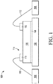
- FIG. 1 illustrates, in simplified cross-sectional view, an exemplary semiconductor device 100 at a stage of manufacture in accordance with an embodiment of the present invention.
- exemplary semiconductor device 100 includes a leadframe and a semiconductor die 106.
- the leadframe includes a flag 102 suitable for attachment of the semiconductor die 106, and plurality of bond terminals 104.
- the leadframe may be formed of any suitable electrically conductive material, such as aluminum, copper, silver, nickel, or iron, or alloys including one or more of these materials, for example.
- the conductive metal may be bare, partially plated, or plated with another metal or an alloy such as iron/nickel alloy, silver, gold, copper, or the like.
- the leadframe is formed from a base metal such as copper and bond terminals 104 include a top surface copper layer formed on the base metal where the top surface copper layer includes copper (Cu) ⁇ 111>.
- the term Cu ⁇ 111> refers to copper having ⁇ 111> grain orientation.
- the leadframe may be formed as conductive traces on a printed circuit board or a substrate (e.g., ceramic or silicon).
- the flag 102 may be any shape, size, or configuration suitable for an attached semiconductor die.
- the flag 102 may be characterized as a downset flag where the plane of the flag 102 is below the plane of the plurality of bond terminals 104.
- the plurality of bond terminals 104 couple electrical signals between locations at the outside of a finished semiconductor device package and locations within the package such as bond pads on the semiconductor die 106.
- the semiconductor die 106 is attached to the flag 102 with an adhesive 108.
- the adhesive may be a solder alloy, an epoxy, or any suitable die-attach material such as a die-attach film, for example.
- semiconductor die 106 may be attached to the flag 102 by way of a eutectic bonding process or sintering process.
- the semiconductor die 106 includes a plurality of bond pads 110 located at the top major surface of the die.
- the bond pads 110 may be formed during multiple processing steps. For example, bond pads 110 may be formed having a first portion formed from a top interconnect or metallization layer, and a second portion formed from a subsequent metal deposition or plating as a top surface layer suitable for bond wire attachment.
- the first portion is formed from a copper or copper alloy interconnect layer and the second portion is formed from a copper deposition or plating as a top surface layer of Cu ⁇ 111>.
- Semiconductor die 106 may be formed from any suitable semiconductor material such as silicon, germanium, gallium arsenide, and the like. Semiconductor die 106 may include any or combination of digital circuits, analog circuits, memory, processor, MEMS, sensors, and the like.
- Bond wires 112 electrically couple bond pads 110 on the semiconductor die 106 to the plurality of bond terminals 104 of the leadframe.
- the bond wires 112 may be formed from a metal comprising copper or copper alloys.
- the bond wires 112 may be attached to the bond pads 110 of the semiconductor die 106 and the leadframe bond terminals 104 with either ball bonds or wedge bonds or a combination of ball bonds and wedge bonds.
- ball bonds may be used to attach a first end of bond wires 112 to bond pads 110 of the semiconductor die 106 and wedge bonds may be used to attach the opposite ends of bond wires 112 to the bond terminals 104 of the leadframe.
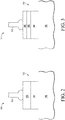
- FIG. 2 illustrates, in simplified cross-sectional view, a more detailed representation of wire bond region 114 of exemplary semiconductor device 100 formed in accordance with embodiment of the present invention.
- Wire bond region 114 includes bond wire 112 bonded at a top surface layer 204 of bond pad 110.
- Top surface layer 204 is formed on a top interconnect metal layer portion 202 of semiconductor die 106.
- the top interconnect layer is characterized as the upper-most, or last interconnect layer of semiconductor die 106 and may generally be connected to other circuitry or other interconnect layers.
- the top interconnect layer is formed from a copper or copper alloy material.
- Cu ⁇ 111> is deposited or plated as a top surface layer (204) on the top interconnect layer portion 202.
- top surface Cu ⁇ 111> layer 204 is formed to have a thickness value in the range of 0.2 to 0.6 ⁇ m (microns). Other embodiments may have other thickness values. In this embodiment, top surface layer 204 is formed to have a concentration of 60% or greater of Cu ⁇ 111 >.
- Bond wire 112 is formed from a copper or copper alloy material. In this embodiment, bond wire 112 is formed to have a concentration of 60% or greater of copper. Because the top surface layer 204 of bond pad 110 is formed from Cu ⁇ 111>, the top surface of layer 204 is less susceptible to oxidation. Accordingly, direct bonding of (copper) bond wire 112 on (copper) bond pad 110 can be accomplished without additional processing steps. A significant advantage having copper bond wires bonded directly on copper bond pads is that intermetallic compound formation and associated corrosion susceptibility are virtually eliminated.
- FIG. 3 illustrates, in simplified cross-sectional view, a more detailed representation of wire bond region 114 of exemplary semiconductor device 100 formed in accordance with another embodiment of the present invention.
- wire bond region 114 includes bond wire 112 bonded at a top surface layer 304 of bond pad 110.
- a thin seed layer 302 of Cu ⁇ 111 > is deposited at the top interconnect layer portion 202.
- a subsequent plating process with copper forms top surface layer 304 as a Cu ⁇ 111 > layer.
- top surface Cu ⁇ 111 > layer 304 is formed to have a thickness value in the range of 0.2 to 0.6 ⁇ m (microns). Other embodiments may have other thickness values.
- top surface layer 304 is formed to have a concentration of 60% or greater of Cu ⁇ 111 >.
- the top interconnect layer is characterized as the upper-most or last interconnect layer of semiconductor die 106 and may generally be used to interconnect other circuitry.
- the top interconnect layer is formed from a copper or copper alloy material.
- bond wire 112 is formed from a copper or copper alloy material, and formed to have a concentration of 60% or greater of copper. Because the top surface layer 304 of bond pad 110 is formed from Cu ⁇ 111 >, the top surface of layer 304 is less susceptible to oxidation. Accordingly, direct bonding of (copper) bond wire 112 on (copper) bond pad 110 can be accomplished without additional processing steps.
- FIG. 4 illustrates, in simplified cross-sectional view, a more detailed representation of a bond terminal 104 of exemplary semiconductor device 100 formed in accordance with embodiment of the present invention.
- Bond terminal 104 includes a surface layer suitable for attachment of a bond wire.
- a top surface layer 404 of bond terminal 104 is formed on a base metal layer portion 402 of the leadframe.
- the base metal layer portion 402 is formed from a copper or copper alloy material. In other embodiments, base metal layer portion 402 may be formed from other metals or alloys.
- Cu ⁇ 111> is deposited as a top surface layer (404) on the top base metal layer portion 402.
- top surface Cu ⁇ 111> layer 404 is formed to have a thickness value in the range of 0.2 to 0.6 ⁇ m (microns). Other embodiments may have other thickness values. In this embodiment, top surface layer 404 is formed to have a concentration of 60% or greater of Cu ⁇ 111 >. Because the top surface layer 404 of bond terminal 104 is formed from Cu ⁇ 111>, the top surface of layer 404 is less susceptible to oxidation. Accordingly, direct bonding of (copper) bond wire on (copper) bond terminal 104 can be accomplished without additional processing steps. A significant advantage having copper bond wires bonded directly on copper bond terminals is that intermetallic compound formation and associated corrosion susceptibility are virtually eliminated.
- FIG. 5 illustrates, in simplified cross-sectional view, a more detailed representation of a bond terminal 104 of exemplary semiconductor device 100 formed in accordance with another embodiment of the present invention.
- Bond terminal 104 includes a surface layer suitable for attachment of a bond wire.
- a thin seed layer 502 of Cu ⁇ 111> is deposited on the base metal layer portion 402 of the leadframe.
- a subsequent plating process with copper forms top surface layer 504 as a Cu ⁇ 111> layer.
- top surface Cu ⁇ 111> layer 504 is formed to have a thickness value in the range of 0.2 to 0.6 ⁇ m (microns). Other embodiments may have other thickness values.
- top surface layer 504 is formed to have a concentration of 60% or greater of Cu ⁇ 111 >.
- top surface layer 504 of bond terminal 104 is formed from Cu ⁇ 111>, the top surface of layer 504 is less susceptible to oxidation. Accordingly, direct bonding of (copper) bond wire on (copper) bond terminal 104 can be accomplished without additional processing steps.
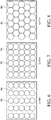
- FIG. 6 through FIG. 8 illustrates, in simplified surface schematic views, various grain orientations in accordance with an embodiment of the present invention.
- FIG. 6 through FIG. 8 shows surface diagrams for copper having ⁇ 110>, ⁇ 100>, and ⁇ 111> grain orientations, respectively.
- FIG. 6 illustrates, in simplified surface schematic view, a diagram of copper having ⁇ 110> grain orientation (Cu ⁇ 110>) in accordance with an embodiment of the present invention.
- Cu ⁇ 110> as depicted in FIG.6 includes the circular shapes 602 are representative of crystal or crystalline grains in the ⁇ 110> orientation.
- Cu ⁇ 110> has the lowest density of a surface plane of copper as shown by the large void area 604 between grains.
- Cu ⁇ 110> is deemed least stable and would generally form a significant amount of oxide when subjected to subsequent heat cycles.
- FIG. 7 illustrates, in simplified surface schematic view, a diagram of copper having ⁇ 100> grain orientation (Cu ⁇ 100>) in accordance with an embodiment of the present invention.
- Cu ⁇ 100> as depicted in FIG. 7 includes circular shapes 702 representative of crystalline grains formed in the ⁇ 100> orientation.
- Cu ⁇ 110> has the next lowest density of a surface plane of copper as shown by the medium void area 704 between grains.
- Cu ⁇ 100> is deemed more stable than Cu ⁇ 110> depicted in FIG. 6 , and would generally form a less significant amount of oxide when subjected to subsequent heat cycles.
- FIG. 8 illustrates, in simplified surface schematic view, a diagram of copper having ⁇ 111> grain orientation (Cu ⁇ 111>) in accordance with an embodiment of the present invention.
- Cu ⁇ 111> as depicted in FIG. 8 includes circular shapes 802 representative of crystalline grains formed in the ⁇ 111> orientation.
- Cu ⁇ 111> has the highest density of a surface plane of copper as shown by the minimal void area 804 between grains.
- Cu ⁇ 111> is deemed more stable than Cu ⁇ 100> depicted in FIG. 7 , and would generally form a very small or negligible amount of oxide when subjected to subsequent heat cycles.
- Cu ⁇ 111> when formed on bonding surfaces provides a superior surface for attaching copper bond wires.
- Another advantage having copper bond wires bonded directly on Cu ⁇ 111> surfaces is that intermetallic compound formation and associated corrosion susceptibility are virtually eliminated.
- a device including a leadframe having a flag and a plurality of bond terminals; a semiconductor die attached to the leadframe at the flag; a bond pad formed on the semiconductor die, the bond pad having a top surface layer comprising copper having ⁇ 111> grain orientation (Cu ⁇ 111 >); and a bond wire having a first end and a second end, the bond wire attached to the bond pad at the first end and attached to one of the bond terminals in the plurality at the second end.
- the bond wire may include a 60% or higher concentration of copper.
- the top surface layer including Cu ⁇ 111> may be formed on a top interconnect layer of the semiconductor die, the top interconnect layer including copper.
- the top surface layer including Cu ⁇ 111> may be formed by depositing a Cu ⁇ 111> seed layer and electroplating with copper.
- the top surface layer including Cu ⁇ 111> may have a thickness in a range of 0.2 ⁇ m (microns) to 0.6 ⁇ m (microns).
- the top surface layer including Cu ⁇ 111> may include a concentration of at least 60% Cu ⁇ 111>.
- a top bonding surface of the one of the bond terminals in the plurality may include Cu ⁇ 111>, the top bonding surface formed on a base metal of the leadframe.
- the top bonding surface of the one of the bond terminals in the plurality may be formed by depositing a Cu ⁇ 111> seed layer and electroplating with copper.
- the top bonding surface of the one of the bond terminals in the plurality may include a concentration of at least 60% Cu ⁇ 111>.
- a device including a leadframe comprising a flag and a bond terminal, a top surface of the bond terminal comprising copper having ⁇ 111> grain orientation (Cu ⁇ 111 >); a semiconductor die attached to the leadframe at the flag; a bond pad formed on the semiconductor die, a top surface of the bond pad comprising Cu ⁇ 111 >; and a bond wire comprising copper having a first end and a second end, the bond wire attached directly to the top surface of the bond pad with a ball bond at the first end and attached to the top surface of the bond terminal at the second end.
- the bond wire may include a 60% or higher concentration of copper.
- the top surface of the bond pad including Cu ⁇ 111> may be formed on a top interconnect layer of the semiconductor die, the top interconnect layer comprising copper.
- the top surface of the bond pad including Cu ⁇ 111> may have a thickness in a range of 0.2 ⁇ m (microns) to 0.6 ⁇ m (microns).
- the top surface of the bond pad Cu ⁇ 111> may include a concentration of at least 60% Cu ⁇ 111>.
- the top surface of the bond terminal including Cu ⁇ 111> may be formed on a base metal of the leadframe, the base metal comprising copper.
- the top surface of the bond terminal including Cu ⁇ 111> may include a concentration of at least 60% Cu ⁇ 111>.
- a method including forming an interconnect layer on a semiconductor die; depositing copper having ⁇ 111> grain orientation (Cu ⁇ 111 >) on at least a portion of the interconnect layer to form a top surface of a bond pad; attaching the semiconductor die to a flag of a leadframe; attaching a first end of a bond wire comprising copper to the top surface of the bond pad; and attaching a second end of the bond wire to a bond terminal of the leadframe.
- the top surface of the bond pad including Cu ⁇ 111> may have a thickness in a range of 0.2 ⁇ m (microns) to 0.6 ⁇ m (microns).
- the bond terminal may include forming a top surface layer of Cu ⁇ 111> on a base metal of the leadframe, the base metal comprising copper.
- the top surface of the bond pad and the top surface layer of the bond terminal each may include a concentration of at least 60% Cu ⁇ 111>.
- a bond pad structure and method of forming the same By forming a top surface layer of copper having a ⁇ 111> grain orientation (Cu ⁇ 111>) on a bond pad, a copper bond wire can be attached without additional processing steps. Copper offers superior conductivity characteristics with modest costs when compared with other choices for pad metals and bond wires.
- the Cu ⁇ 111> top surface layer may be formed by deposition or plating.
- the Cu ⁇ 111> top surface layer has minimal oxide growth due to the grain density and allows for direct bonding with a copper bond wire. By directly attaching copper bond wires on Cu ⁇ 111> bond pads, intermetallic compound formation and associated corrosion susceptibility are virtually eliminated.
Landscapes
- Wire Bonding (AREA)
- Engineering & Computer Science (AREA)
- Manufacturing & Machinery (AREA)
- Die Bonding (AREA)
Abstract
A semiconductor device includes a leadframe having a flag (102) and a plurality of bond terminals (104). A semiconductor die (106) is attached to the leadframe at the flag (102). A bond pad (110) is formed on the semiconductor die (106). A top surface layer of the bond pad (110) includes copper having a predetermined <111> grain orientation. A bond wire (112) includes a first end and a second end. The bond wire (112) is attached to the bond pad (110) at the first end and attached to one of the bond terminals (104) in the plurality at the second end.
Description
- This disclosure relates generally to semiconductor devices, and more specifically, to bond pad structure and formation for semiconductor device packaging.
- Semiconductor devices are often found in a large spectrum of electronic products - from sewing machines to washing machines, from automobiles to cellular telephones, and so on. Such semiconductor devices generally include an integrated circuit die which communicates with the other devices outside of a package by way of bond wires. As technology progresses, semiconductor manufacturing continues to seek ways to reduce costs and improve reliability in these semiconductor devices.
- The present invention is illustrated by way of example and is not limited by the accompanying figures, in which like references indicate similar elements. Elements in the figures are illustrated for simplicity and clarity and have not necessarily been drawn to scale.
-
FIG. 1 illustrates, in simplified cross-sectional view, an exemplary semiconductor device formed in accordance with an embodiment of the present invention. -
FIG. 2 illustrates, in simplified cross-sectional view, a more detailed bond pad of exemplary semiconductor device formed in accordance with embodiment of the present invention. -
FIG. 3 illustrates, in simplified cross-sectional view, a more detailed bond pad of exemplary semiconductor device formed in accordance with another embodiment of the present invention. -
FIG. 4 illustrates, in simplified cross-sectional view, a more detailed bond terminal of exemplary semiconductor device formed in accordance with embodiment of the present invention. -
FIG. 5 illustrates, in simplified cross-sectional view, a more detailed bond terminal of exemplary semiconductor device formed in accordance with another embodiment of the present invention. -
FIG. 6 through FIG. 8 illustrates, in simplified surface schematic views, various grain orientations in accordance with an embodiment of the present invention. - Generally, there is provided, a bond pad structure and method of forming the same. By forming a top surface layer of copper having a <111> grain orientation (Cu <111>) on a bond pad, a copper bond wire can be attached without additional processing steps. Copper offers superior conductivity characteristics with modest costs when compared with other choices for pad metals and bond wires. The Cu <111 > top surface layer may be formed by deposition or plating. The Cu <111> top surface layer has minimal oxide growth due to the grain density and allows for direct bonding with a copper bond wire. By directly attaching copper bond wires on Cu <111> bond pads, intermetallic compound formation and associated corrosion susceptibility are virtually eliminated.
-
FIG. 1 illustrates, in simplified cross-sectional view, anexemplary semiconductor device 100 at a stage of manufacture in accordance with an embodiment of the present invention. At this stage,exemplary semiconductor device 100 includes a leadframe and asemiconductor die 106. The leadframe includes aflag 102 suitable for attachment of thesemiconductor die 106, and plurality ofbond terminals 104. The leadframe may be formed of any suitable electrically conductive material, such as aluminum, copper, silver, nickel, or iron, or alloys including one or more of these materials, for example. The conductive metal may be bare, partially plated, or plated with another metal or an alloy such as iron/nickel alloy, silver, gold, copper, or the like. In this embodiment, the leadframe is formed from a base metal such as copper andbond terminals 104 include a top surface copper layer formed on the base metal where the top surface copper layer includes copper (Cu) <111>. As used herein, the term Cu <111> refers to copper having <111> grain orientation. In some embodiments, the leadframe may be formed as conductive traces on a printed circuit board or a substrate (e.g., ceramic or silicon). - The
flag 102 may be any shape, size, or configuration suitable for an attached semiconductor die. In some embodiments, theflag 102 may be characterized as a downset flag where the plane of theflag 102 is below the plane of the plurality ofbond terminals 104. The plurality ofbond terminals 104 couple electrical signals between locations at the outside of a finished semiconductor device package and locations within the package such as bond pads on thesemiconductor die 106. - The
semiconductor die 106 is attached to theflag 102 with an adhesive 108. The adhesive may be a solder alloy, an epoxy, or any suitable die-attach material such as a die-attach film, for example. In some embodiments, semiconductor die 106 may be attached to theflag 102 by way of a eutectic bonding process or sintering process. The semiconductor die 106 includes a plurality ofbond pads 110 located at the top major surface of the die. Thebond pads 110 may be formed during multiple processing steps. For example,bond pads 110 may be formed having a first portion formed from a top interconnect or metallization layer, and a second portion formed from a subsequent metal deposition or plating as a top surface layer suitable for bond wire attachment. In this embodiment, the first portion is formed from a copper or copper alloy interconnect layer and the second portion is formed from a copper deposition or plating as a top surface layer of Cu <111>. Semiconductor die 106 may be formed from any suitable semiconductor material such as silicon, germanium, gallium arsenide, and the like. Semiconductor die 106 may include any or combination of digital circuits, analog circuits, memory, processor, MEMS, sensors, and the like. -
Bond wires 112 electricallycouple bond pads 110 on the semiconductor die 106 to the plurality ofbond terminals 104 of the leadframe. Thebond wires 112 may be formed from a metal comprising copper or copper alloys. Thebond wires 112 may be attached to thebond pads 110 of thesemiconductor die 106 and theleadframe bond terminals 104 with either ball bonds or wedge bonds or a combination of ball bonds and wedge bonds. For example, ball bonds may be used to attach a first end ofbond wires 112 tobond pads 110 of thesemiconductor die 106 and wedge bonds may be used to attach the opposite ends ofbond wires 112 to thebond terminals 104 of the leadframe. -
FIG. 2 illustrates, in simplified cross-sectional view, a more detailed representation ofwire bond region 114 ofexemplary semiconductor device 100 formed in accordance with embodiment of the present invention.Wire bond region 114 includesbond wire 112 bonded at atop surface layer 204 ofbond pad 110.Top surface layer 204 is formed on a top interconnectmetal layer portion 202 of semiconductor die 106. In this embodiment, the top interconnect layer is characterized as the upper-most, or last interconnect layer ofsemiconductor die 106 and may generally be connected to other circuitry or other interconnect layers. The top interconnect layer is formed from a copper or copper alloy material. To formbond pad 110, Cu <111> is deposited or plated as a top surface layer (204) on the topinterconnect layer portion 202. In this embodiment, top surface Cu <111>layer 204 is formed to have a thickness value in the range of 0.2 to 0.6 µm (microns). Other embodiments may have other thickness values. In this embodiment,top surface layer 204 is formed to have a concentration of 60% or greater of Cu <111 >.Bond wire 112 is formed from a copper or copper alloy material. In this embodiment,bond wire 112 is formed to have a concentration of 60% or greater of copper. Because thetop surface layer 204 ofbond pad 110 is formed from Cu <111>, the top surface oflayer 204 is less susceptible to oxidation. Accordingly, direct bonding of (copper)bond wire 112 on (copper)bond pad 110 can be accomplished without additional processing steps. A significant advantage having copper bond wires bonded directly on copper bond pads is that intermetallic compound formation and associated corrosion susceptibility are virtually eliminated. -
FIG. 3 illustrates, in simplified cross-sectional view, a more detailed representation ofwire bond region 114 ofexemplary semiconductor device 100 formed in accordance with another embodiment of the present invention. In this embodiment,wire bond region 114 includesbond wire 112 bonded at atop surface layer 304 ofbond pad 110. Here, athin seed layer 302 of Cu <111 > is deposited at the topinterconnect layer portion 202. A subsequent plating process with copper formstop surface layer 304 as a Cu <111 > layer. In this embodiment, top surface Cu <111 >layer 304 is formed to have a thickness value in the range of 0.2 to 0.6 µm (microns). Other embodiments may have other thickness values. In this embodiment,top surface layer 304 is formed to have a concentration of 60% or greater of Cu <111 >. In this embodiment, the top interconnect layer is characterized as the upper-most or last interconnect layer of semiconductor die 106 and may generally be used to interconnect other circuitry. The top interconnect layer is formed from a copper or copper alloy material. In this embodiment,bond wire 112 is formed from a copper or copper alloy material, and formed to have a concentration of 60% or greater of copper. Because thetop surface layer 304 ofbond pad 110 is formed from Cu <111 >, the top surface oflayer 304 is less susceptible to oxidation. Accordingly, direct bonding of (copper)bond wire 112 on (copper)bond pad 110 can be accomplished without additional processing steps. -
FIG. 4 illustrates, in simplified cross-sectional view, a more detailed representation of abond terminal 104 ofexemplary semiconductor device 100 formed in accordance with embodiment of the present invention.Bond terminal 104 includes a surface layer suitable for attachment of a bond wire. In this embodiment, atop surface layer 404 ofbond terminal 104 is formed on a basemetal layer portion 402 of the leadframe. The basemetal layer portion 402 is formed from a copper or copper alloy material. In other embodiments, basemetal layer portion 402 may be formed from other metals or alloys. To formbond terminal 104, Cu <111> is deposited as a top surface layer (404) on the top basemetal layer portion 402. In this embodiment, top surface Cu <111>layer 404 is formed to have a thickness value in the range of 0.2 to 0.6 µm (microns). Other embodiments may have other thickness values. In this embodiment,top surface layer 404 is formed to have a concentration of 60% or greater of Cu <111 >. Because thetop surface layer 404 ofbond terminal 104 is formed from Cu <111>, the top surface oflayer 404 is less susceptible to oxidation. Accordingly, direct bonding of (copper) bond wire on (copper)bond terminal 104 can be accomplished without additional processing steps. A significant advantage having copper bond wires bonded directly on copper bond terminals is that intermetallic compound formation and associated corrosion susceptibility are virtually eliminated. -
FIG. 5 illustrates, in simplified cross-sectional view, a more detailed representation of abond terminal 104 ofexemplary semiconductor device 100 formed in accordance with another embodiment of the present invention.Bond terminal 104 includes a surface layer suitable for attachment of a bond wire. In this embodiment, athin seed layer 502 of Cu <111> is deposited on the basemetal layer portion 402 of the leadframe. A subsequent plating process with copper forms topsurface layer 504 as a Cu <111> layer. In this embodiment, top surface Cu <111>layer 504 is formed to have a thickness value in the range of 0.2 to 0.6 µm (microns). Other embodiments may have other thickness values. In this embodiment,top surface layer 504 is formed to have a concentration of 60% or greater of Cu <111 >. Because thetop surface layer 504 ofbond terminal 104 is formed from Cu <111>, the top surface oflayer 504 is less susceptible to oxidation. Accordingly, direct bonding of (copper) bond wire on (copper)bond terminal 104 can be accomplished without additional processing steps. -
FIG. 6 through FIG. 8 illustrates, in simplified surface schematic views, various grain orientations in accordance with an embodiment of the present invention.FIG. 6 through FIG. 8 shows surface diagrams for copper having <110>, <100>, and <111> grain orientations, respectively. -
FIG. 6 illustrates, in simplified surface schematic view, a diagram of copper having <110> grain orientation (Cu <110>) in accordance with an embodiment of the present invention. Cu <110> as depicted inFIG.6 , includes thecircular shapes 602 are representative of crystal or crystalline grains in the <110> orientation. Among the grain orientations depicted inFIG. 6 through FIG. 8 , Cu <110> has the lowest density of a surface plane of copper as shown by thelarge void area 604 between grains. Cu <110> is deemed least stable and would generally form a significant amount of oxide when subjected to subsequent heat cycles. -
FIG. 7 illustrates, in simplified surface schematic view, a diagram of copper having <100> grain orientation (Cu <100>) in accordance with an embodiment of the present invention. Cu <100> as depicted inFIG. 7 , includescircular shapes 702 representative of crystalline grains formed in the <100> orientation. Among the grain orientations depicted inFIG. 6 through FIG. 8 , Cu <110> has the next lowest density of a surface plane of copper as shown by themedium void area 704 between grains. Cu <100> is deemed more stable than Cu <110> depicted inFIG. 6 , and would generally form a less significant amount of oxide when subjected to subsequent heat cycles. -
FIG. 8 illustrates, in simplified surface schematic view, a diagram of copper having <111> grain orientation (Cu <111>) in accordance with an embodiment of the present invention. Cu <111> as depicted inFIG. 8 , includescircular shapes 802 representative of crystalline grains formed in the <111> orientation. Among the grain orientations depicted inFIG. 6 through FIG. 8 , Cu <111> has the highest density of a surface plane of copper as shown by theminimal void area 804 between grains. Cu <111> is deemed more stable than Cu <100> depicted inFIG. 7 , and would generally form a very small or negligible amount of oxide when subjected to subsequent heat cycles. As such, Cu <111> when formed on bonding surfaces, provides a superior surface for attaching copper bond wires. Another advantage having copper bond wires bonded directly on Cu <111> surfaces is that intermetallic compound formation and associated corrosion susceptibility are virtually eliminated. - Generally, there is provided, a device including a leadframe having a flag and a plurality of bond terminals; a semiconductor die attached to the leadframe at the flag; a bond pad formed on the semiconductor die, the bond pad having a top surface layer comprising copper having <111> grain orientation (Cu <111 >); and a bond wire having a first end and a second end, the bond wire attached to the bond pad at the first end and attached to one of the bond terminals in the plurality at the second end. The bond wire may include a 60% or higher concentration of copper. The top surface layer including Cu <111> may be formed on a top interconnect layer of the semiconductor die, the top interconnect layer including copper. The top surface layer including Cu <111> may be formed by depositing a Cu <111> seed layer and electroplating with copper. The top surface layer including Cu <111> may have a thickness in a range of 0.2 µm (microns) to 0.6 µm (microns). The top surface layer including Cu <111> may include a concentration of at least 60% Cu <111>. A top bonding surface of the one of the bond terminals in the plurality may include Cu <111>, the top bonding surface formed on a base metal of the leadframe. The top bonding surface of the one of the bond terminals in the plurality may be formed by depositing a Cu <111> seed layer and electroplating with copper. The top bonding surface of the one of the bond terminals in the plurality may include a concentration of at least 60% Cu <111>.
- In another embodiment, there is provided, a device including a leadframe comprising a flag and a bond terminal, a top surface of the bond terminal comprising copper having <111> grain orientation (Cu <111 >); a semiconductor die attached to the leadframe at the flag; a bond pad formed on the semiconductor die, a top surface of the bond pad comprising Cu <111 >; and a bond wire comprising copper having a first end and a second end, the bond wire attached directly to the top surface of the bond pad with a ball bond at the first end and attached to the top surface of the bond terminal at the second end. The bond wire may include a 60% or higher concentration of copper. The top surface of the bond pad including Cu <111> may be formed on a top interconnect layer of the semiconductor die, the top interconnect layer comprising copper. The top surface of the bond pad including Cu <111> may have a thickness in a range of 0.2 µm (microns) to 0.6 µm (microns). The top surface of the bond pad Cu <111> may include a concentration of at least 60% Cu <111>. The top surface of the bond terminal including Cu <111> may be formed on a base metal of the leadframe, the base metal comprising copper. The top surface of the bond terminal including Cu <111> may include a concentration of at least 60% Cu <111>.
- In yet another embodiment, there is provided, a method including forming an interconnect layer on a semiconductor die; depositing copper having <111> grain orientation (Cu <111 >) on at least a portion of the interconnect layer to form a top surface of a bond pad; attaching the semiconductor die to a flag of a leadframe; attaching a first end of a bond wire comprising copper to the top surface of the bond pad; and attaching a second end of the bond wire to a bond terminal of the leadframe. The top surface of the bond pad including Cu <111> may have a thickness in a range of 0.2 µm (microns) to 0.6 µm (microns). The bond terminal may include forming a top surface layer of Cu <111> on a base metal of the leadframe, the base metal comprising copper. The top surface of the bond pad and the top surface layer of the bond terminal each may include a concentration of at least 60% Cu <111>.
- By now it should be appreciated that there has been provided, a bond pad structure and method of forming the same. By forming a top surface layer of copper having a <111> grain orientation (Cu <111>) on a bond pad, a copper bond wire can be attached without additional processing steps. Copper offers superior conductivity characteristics with modest costs when compared with other choices for pad metals and bond wires. The Cu <111> top surface layer may be formed by deposition or plating. The Cu <111> top surface layer has minimal oxide growth due to the grain density and allows for direct bonding with a copper bond wire. By directly attaching copper bond wires on Cu <111> bond pads, intermetallic compound formation and associated corrosion susceptibility are virtually eliminated.
- Although the invention is described herein with reference to specific embodiments, various modifications and changes can be made without departing from the scope of the present invention as set forth in the claims below. Accordingly, the specification and figures are to be regarded in an illustrative rather than a restrictive sense, and all such modifications are intended to be included within the scope of the present invention. Any benefits, advantages, or solutions to problems that are described herein with regard to specific embodiments are not intended to be construed as a critical, required, or essential feature or element of any or all the claims.
- Furthermore, the terms "a" or "an," as used herein, are defined as one or more than one. Also, the use of introductory phrases such as "at least one" and "one or more" in the claims should not be construed to imply that the introduction of another claim element by the indefinite articles "a" or "an" limits any particular claim containing such introduced claim element to inventions containing only one such element, even when the same claim includes the introductory phrases "one or more" or "at least one" and indefinite articles such as "a" or "an." The same holds true for the use of definite articles.
- Unless stated otherwise, terms such as "first" and "second" are used to arbitrarily distinguish between the elements such terms describe. Thus, these terms are not necessarily intended to indicate temporal or other prioritization of such elements.
Claims (14)
- A device, comprising:a leadframe having a flag (102) and a plurality of bond terminals (104);a semiconductor die (106) attached to the leadframe at the flag;a bond pad (110) formed on the semiconductor die, the bond pad having a top surface layer (204, 304), comprising copper having <111> grain orientation, Cu <111>; anda bond wire (112) having a first end and a second end, the bond wire attached to the bond pad at the first end and attached to one of the bond terminals in the plurality at the second end.
- The device of claim 1, wherein the bond wire comprises a 60% or higher concentration of copper.
- The device of claim 1 or claim 2, wherein the top surface layer comprising Cu <111> is formed on a top interconnect layer (202) of the semiconductor die, the top interconnect layer comprising copper.
- The device of claim 3, wherein the top surface layer comprising Cu <111> is formed by depositing a Cu <111> seed layer (302) and electroplating with copper.
- The device of any preceding claim, wherein the top surface layer comprising Cu <111> has a thickness in a range of 0.2 µm to 0.6 µm.
- The device of any preceding claim, wherein the top surface layer comprising Cu <111 > comprises a concentration of at least 60% Cu <111 >.
- The device of any preceding claim, wherein a top bonding surface (404, 504) of the one of the bond terminals in the plurality comprises Cu <111 >, the top bonding surface formed on a base metal (402) of the leadframe.
- The device of claim 7, wherein the top bonding surface of the one of the bond terminals in the plurality is formed by depositing a Cu <111> seed layer (502) and electroplating with copper.
- The device of claim 7 or claim 8, wherein the top bonding surface of the one of the bond terminals in the plurality comprises a concentration of at least 60% Cu <111>.
- The device of any preceding claim, wherein the bond wire is attached directly to the top surface of the bond pad with a ball bond at the first end and attached to the top surface of the one of the bond terminals in the plurality at the second end.
- A method comprising:forming an interconnect layer (202) on a semiconductor die (106);depositing copper having <111> grain orientation, Cu <111 >, on at least a portion of the interconnect layer to form a top surface (204, 304) of a bond pad (110);attaching the semiconductor die to a flag (102) of a leadframe;attaching a first end of a bond wire (112) comprising copper to the top surface of the bond pad; andattaching a second end of the bond wire to a bond terminal (104) of the leadframe.
- The method of claim 11, wherein the top surface of the bond pad comprising Cu <111> has a thickness in a range of 0.2 µm to 0.6 µm.
- The method of claim 11 or claim 12, wherein the bond terminal comprises forming a top surface layer (404) of Cu <111> on a base metal (402) of the leadframe, the base metal comprising copper.
- The method of claim 13, wherein the top surface of the bond pad and/or the top surface layer of the bond terminal comprise a concentration of at least 60% Cu <111 >.
Applications Claiming Priority (1)
| Application Number | Priority Date | Filing Date | Title |
|---|---|---|---|
| US15/843,615 US10147697B1 (en) | 2017-12-15 | 2017-12-15 | Bond pad structure for semiconductor device packaging |
Publications (1)
| Publication Number | Publication Date |
|---|---|
| EP3499565A1 true EP3499565A1 (en) | 2019-06-19 |
Family
ID=64452172
Family Applications (1)
| Application Number | Title | Priority Date | Filing Date |
|---|---|---|---|
| EP18211305.0A Withdrawn EP3499565A1 (en) | 2017-12-15 | 2018-12-10 | Bond pad structure for semiconductor device packaging |
Country Status (2)
| Country | Link |
|---|---|
| US (1) | US10147697B1 (en) |
| EP (1) | EP3499565A1 (en) |
Families Citing this family (3)
| Publication number | Priority date | Publication date | Assignee | Title |
|---|---|---|---|---|
| JP6736716B1 (en) * | 2019-03-22 | 2020-08-05 | 大口マテリアル株式会社 | Lead frame |
| US20240145350A1 (en) * | 2022-10-31 | 2024-05-02 | Mediatek Inc. | Semiconductor device and manufacturing method thereof |
| US20250300105A1 (en) * | 2024-03-21 | 2025-09-25 | Wolfspeed, Inc. | Power devices with multiple metal layer thicknesses |
Citations (3)
| Publication number | Priority date | Publication date | Assignee | Title |
|---|---|---|---|---|
| US20100052139A1 (en) * | 2008-09-01 | 2010-03-04 | Hitachi, Ltd. | Semiconductor device and method for manufacturing the same, and semiconductor sealing resin |
| US20110260307A1 (en) * | 2010-04-27 | 2011-10-27 | Infineon Technologies Ag | Integrated circuit including bond wire directly bonded to pad |
| US20150037603A1 (en) * | 2013-07-30 | 2015-02-05 | GlobalFoundries, Inc. | Articles including metal structures having maximized bond adhesion and bond reliability, and methods of forming the same |
Family Cites Families (7)
| Publication number | Priority date | Publication date | Assignee | Title |
|---|---|---|---|---|
| US5316802A (en) | 1992-02-20 | 1994-05-31 | Nissin Electric Co., Ltd. | Method of forming copper film on substrate |
| US6593643B1 (en) * | 1999-04-08 | 2003-07-15 | Shinko Electric Industries Co., Ltd. | Semiconductor device lead frame |
| JP4603812B2 (en) | 2003-05-12 | 2010-12-22 | ローム・アンド・ハース・エレクトロニック・マテリアルズ,エル.エル.シー. | Improved tin plating method |
| WO2008010378A1 (en) | 2006-07-21 | 2008-01-24 | Kabushiki Kaisha Kobe Seiko Sho | Copper alloy sheets for electrical/electronic part |
| US8097102B2 (en) | 2008-12-08 | 2012-01-17 | Dowa Metaltech Co., Ltd. | Cu-Ti-based copper alloy sheet material and method of manufacturing same |
| JP5634149B2 (en) * | 2010-07-16 | 2014-12-03 | ルネサスエレクトロニクス株式会社 | Semiconductor device |
| JP2016219707A (en) * | 2015-05-25 | 2016-12-22 | 富士電機株式会社 | Semiconductor device and manufacturing method of the same |
-
2017
- 2017-12-15 US US15/843,615 patent/US10147697B1/en active Active
-
2018
- 2018-12-10 EP EP18211305.0A patent/EP3499565A1/en not_active Withdrawn
Patent Citations (3)
| Publication number | Priority date | Publication date | Assignee | Title |
|---|---|---|---|---|
| US20100052139A1 (en) * | 2008-09-01 | 2010-03-04 | Hitachi, Ltd. | Semiconductor device and method for manufacturing the same, and semiconductor sealing resin |
| US20110260307A1 (en) * | 2010-04-27 | 2011-10-27 | Infineon Technologies Ag | Integrated circuit including bond wire directly bonded to pad |
| US20150037603A1 (en) * | 2013-07-30 | 2015-02-05 | GlobalFoundries, Inc. | Articles including metal structures having maximized bond adhesion and bond reliability, and methods of forming the same |
Also Published As
| Publication number | Publication date |
|---|---|
| US10147697B1 (en) | 2018-12-04 |
Similar Documents
| Publication | Publication Date | Title |
|---|---|---|
| US10325876B2 (en) | Surface finish for wirebonding | |
| US6781243B1 (en) | Leadless leadframe package substitute and stack package | |
| US8188579B1 (en) | Semiconductor device including leadframe having power bars and increased I/O | |
| US9059185B2 (en) | Copper leadframe finish for copper wire bonding | |
| US7413934B2 (en) | Leadframes for improved moisture reliability and enhanced solderability of semiconductor devices | |
| TWI295846B (en) | Semiconductor device having post-mold nickel/palladium/gold plated leads | |
| US7788800B2 (en) | Method for fabricating a leadframe | |
| US10147697B1 (en) | Bond pad structure for semiconductor device packaging | |
| KR20120008462A (en) | Semiconductor devices | |
| US10741415B2 (en) | Thermosonically bonded connection for flip chip packages | |
| US8703544B2 (en) | Electronic component employing a layered frame | |
| EP4086952A1 (en) | Semiconductor device packaging leadframe assembly and method therefor | |
| US20250239462A1 (en) | Immersion plating process for an integrated circuit | |
| US20140367859A1 (en) | Tin-based wirebond structures | |
| US10366946B2 (en) | Connection member with bulk body and electrically and thermally conductive coating | |
| KR102222146B1 (en) | Low-Cost Semiconductor package with metal structure | |
| EP4525027A1 (en) | Semiconductor device with enhanced solderability and method therefor | |
| KR100544274B1 (en) | Metal lamination structure of stud bump substrate | |
| JP3346458B2 (en) | Wiring board having semiconductor chip bonding leads and semiconductor device | |
| JPH03206633A (en) | Semiconductor device | |
| JPS6351649A (en) | Semiconductor device | |
| JPS6129139A (en) | Semiconductor device | |
| KR20020065733A (en) | Semiconductor package and method for the same | |
| KR20020065729A (en) | Semicoductor package | |
| JPH02174253A (en) | Electronic parts package with rhenium layer at metal part |
Legal Events
| Date | Code | Title | Description |
|---|---|---|---|
| PUAI | Public reference made under article 153(3) epc to a published international application that has entered the european phase |
Free format text: ORIGINAL CODE: 0009012 |
|
| STAA | Information on the status of an ep patent application or granted ep patent |
Free format text: STATUS: THE APPLICATION HAS BEEN PUBLISHED |
|
| AK | Designated contracting states |
Kind code of ref document: A1 Designated state(s): AL AT BE BG CH CY CZ DE DK EE ES FI FR GB GR HR HU IE IS IT LI LT LU LV MC MK MT NL NO PL PT RO RS SE SI SK SM TR |
|
| AX | Request for extension of the european patent |
Extension state: BA ME |
|
| STAA | Information on the status of an ep patent application or granted ep patent |
Free format text: STATUS: THE APPLICATION IS DEEMED TO BE WITHDRAWN |
|
| 18D | Application deemed to be withdrawn |
Effective date: 20191220 |