EP3499552A1 - Semiconductor device and method of manufacture - Google Patents
Semiconductor device and method of manufacture Download PDFInfo
- Publication number
- EP3499552A1 EP3499552A1 EP17207326.4A EP17207326A EP3499552A1 EP 3499552 A1 EP3499552 A1 EP 3499552A1 EP 17207326 A EP17207326 A EP 17207326A EP 3499552 A1 EP3499552 A1 EP 3499552A1
- Authority
- EP
- European Patent Office
- Prior art keywords
- metal layer
- semiconductor device
- electrical contacts
- package body
- semiconductor
- Prior art date
- Legal status (The legal status is an assumption and is not a legal conclusion. Google has not performed a legal analysis and makes no representation as to the accuracy of the status listed.)
- Withdrawn
Links
Images


Classifications
-
- H—ELECTRICITY
- H10—SEMICONDUCTOR DEVICES; ELECTRIC SOLID-STATE DEVICES NOT OTHERWISE PROVIDED FOR
- H10W—GENERIC PACKAGES, INTERCONNECTIONS, CONNECTORS OR OTHER CONSTRUCTIONAL DETAILS OF DEVICES COVERED BY CLASS H10
- H10W74/00—Encapsulations, e.g. protective coatings
- H10W74/01—Manufacture or treatment
- H10W74/016—Manufacture or treatment using moulds
-
- H—ELECTRICITY
- H10—SEMICONDUCTOR DEVICES; ELECTRIC SOLID-STATE DEVICES NOT OTHERWISE PROVIDED FOR
- H10W—GENERIC PACKAGES, INTERCONNECTIONS, CONNECTORS OR OTHER CONSTRUCTIONAL DETAILS OF DEVICES COVERED BY CLASS H10
- H10W74/00—Encapsulations, e.g. protective coatings
- H10W74/01—Manufacture or treatment
-
- H—ELECTRICITY
- H10—SEMICONDUCTOR DEVICES; ELECTRIC SOLID-STATE DEVICES NOT OTHERWISE PROVIDED FOR
- H10P—GENERIC PROCESSES OR APPARATUS FOR THE MANUFACTURE OR TREATMENT OF DEVICES COVERED BY CLASS H10
- H10P54/00—Cutting or separating of wafers, substrates or parts of devices
-
- H—ELECTRICITY
- H10—SEMICONDUCTOR DEVICES; ELECTRIC SOLID-STATE DEVICES NOT OTHERWISE PROVIDED FOR
- H10W—GENERIC PACKAGES, INTERCONNECTIONS, CONNECTORS OR OTHER CONSTRUCTIONAL DETAILS OF DEVICES COVERED BY CLASS H10
- H10W20/00—Interconnections in chips, wafers or substrates
- H10W20/40—Interconnections external to wafers or substrates, e.g. back-end-of-line [BEOL] metallisations or vias connecting to gate electrodes
-
- H—ELECTRICITY
- H10—SEMICONDUCTOR DEVICES; ELECTRIC SOLID-STATE DEVICES NOT OTHERWISE PROVIDED FOR
- H10W—GENERIC PACKAGES, INTERCONNECTIONS, CONNECTORS OR OTHER CONSTRUCTIONAL DETAILS OF DEVICES COVERED BY CLASS H10
- H10W72/00—Interconnections or connectors in packages
- H10W72/30—Die-attach connectors
-
- H—ELECTRICITY
- H10—SEMICONDUCTOR DEVICES; ELECTRIC SOLID-STATE DEVICES NOT OTHERWISE PROVIDED FOR
- H10W—GENERIC PACKAGES, INTERCONNECTIONS, CONNECTORS OR OTHER CONSTRUCTIONAL DETAILS OF DEVICES COVERED BY CLASS H10
- H10W74/00—Encapsulations, e.g. protective coatings
- H10W74/01—Manufacture or treatment
- H10W74/014—Manufacture or treatment using batch processing
-
- H—ELECTRICITY
- H10—SEMICONDUCTOR DEVICES; ELECTRIC SOLID-STATE DEVICES NOT OTHERWISE PROVIDED FOR
- H10W—GENERIC PACKAGES, INTERCONNECTIONS, CONNECTORS OR OTHER CONSTRUCTIONAL DETAILS OF DEVICES COVERED BY CLASS H10
- H10W74/00—Encapsulations, e.g. protective coatings
- H10W74/01—Manufacture or treatment
- H10W74/019—Manufacture or treatment using temporary auxiliary substrates
-
- H—ELECTRICITY
- H10—SEMICONDUCTOR DEVICES; ELECTRIC SOLID-STATE DEVICES NOT OTHERWISE PROVIDED FOR
- H10W—GENERIC PACKAGES, INTERCONNECTIONS, CONNECTORS OR OTHER CONSTRUCTIONAL DETAILS OF DEVICES COVERED BY CLASS H10
- H10W74/00—Encapsulations, e.g. protective coatings
- H10W74/10—Encapsulations, e.g. protective coatings characterised by their shape or disposition
- H10W74/111—Encapsulations, e.g. protective coatings characterised by their shape or disposition the semiconductor body being completely enclosed
-
- H—ELECTRICITY
- H10—SEMICONDUCTOR DEVICES; ELECTRIC SOLID-STATE DEVICES NOT OTHERWISE PROVIDED FOR
- H10W—GENERIC PACKAGES, INTERCONNECTIONS, CONNECTORS OR OTHER CONSTRUCTIONAL DETAILS OF DEVICES COVERED BY CLASS H10
- H10W74/00—Encapsulations, e.g. protective coatings
- H10W74/10—Encapsulations, e.g. protective coatings characterised by their shape or disposition
- H10W74/131—Encapsulations, e.g. protective coatings characterised by their shape or disposition the semiconductor body being only partially enclosed
- H10W74/137—Encapsulations, e.g. protective coatings characterised by their shape or disposition the semiconductor body being only partially enclosed the encapsulations being directly on the semiconductor body
-
- H—ELECTRICITY
- H10—SEMICONDUCTOR DEVICES; ELECTRIC SOLID-STATE DEVICES NOT OTHERWISE PROVIDED FOR
- H10W—GENERIC PACKAGES, INTERCONNECTIONS, CONNECTORS OR OTHER CONSTRUCTIONAL DETAILS OF DEVICES COVERED BY CLASS H10
- H10W74/00—Encapsulations, e.g. protective coatings
- H10W74/10—Encapsulations, e.g. protective coatings characterised by their shape or disposition
- H10W74/131—Encapsulations, e.g. protective coatings characterised by their shape or disposition the semiconductor body being only partially enclosed
- H10W74/141—Encapsulations, e.g. protective coatings characterised by their shape or disposition the semiconductor body being only partially enclosed the encapsulations being on at least the sidewalls of the semiconductor body
-
- H—ELECTRICITY
- H10—SEMICONDUCTOR DEVICES; ELECTRIC SOLID-STATE DEVICES NOT OTHERWISE PROVIDED FOR
- H10W—GENERIC PACKAGES, INTERCONNECTIONS, CONNECTORS OR OTHER CONSTRUCTIONAL DETAILS OF DEVICES COVERED BY CLASS H10
- H10W95/00—Packaging processes not covered by the other groups of this subclass
-
- H—ELECTRICITY
- H10—SEMICONDUCTOR DEVICES; ELECTRIC SOLID-STATE DEVICES NOT OTHERWISE PROVIDED FOR
- H10W—GENERIC PACKAGES, INTERCONNECTIONS, CONNECTORS OR OTHER CONSTRUCTIONAL DETAILS OF DEVICES COVERED BY CLASS H10
- H10W70/00—Package substrates; Interposers; Redistribution layers [RDL]
- H10W70/01—Manufacture or treatment
- H10W70/05—Manufacture or treatment of insulating or insulated package substrates, or of interposers, or of redistribution layers
-
- H—ELECTRICITY
- H10—SEMICONDUCTOR DEVICES; ELECTRIC SOLID-STATE DEVICES NOT OTHERWISE PROVIDED FOR
- H10W—GENERIC PACKAGES, INTERCONNECTIONS, CONNECTORS OR OTHER CONSTRUCTIONAL DETAILS OF DEVICES COVERED BY CLASS H10
- H10W70/00—Package substrates; Interposers; Redistribution layers [RDL]
- H10W70/60—Insulating or insulated package substrates; Interposers; Redistribution layers
-
- H—ELECTRICITY
- H10—SEMICONDUCTOR DEVICES; ELECTRIC SOLID-STATE DEVICES NOT OTHERWISE PROVIDED FOR
- H10W—GENERIC PACKAGES, INTERCONNECTIONS, CONNECTORS OR OTHER CONSTRUCTIONAL DETAILS OF DEVICES COVERED BY CLASS H10
- H10W70/00—Package substrates; Interposers; Redistribution layers [RDL]
- H10W70/60—Insulating or insulated package substrates; Interposers; Redistribution layers
- H10W70/62—Insulating or insulated package substrates; Interposers; Redistribution layers characterised by their interconnections
- H10W70/65—Shapes or dispositions of interconnections
-
- H—ELECTRICITY
- H10—SEMICONDUCTOR DEVICES; ELECTRIC SOLID-STATE DEVICES NOT OTHERWISE PROVIDED FOR
- H10W—GENERIC PACKAGES, INTERCONNECTIONS, CONNECTORS OR OTHER CONSTRUCTIONAL DETAILS OF DEVICES COVERED BY CLASS H10
- H10W70/00—Package substrates; Interposers; Redistribution layers [RDL]
- H10W70/60—Insulating or insulated package substrates; Interposers; Redistribution layers
- H10W70/62—Insulating or insulated package substrates; Interposers; Redistribution layers characterised by their interconnections
- H10W70/65—Shapes or dispositions of interconnections
- H10W70/652—Cross-sectional shapes
-
- H—ELECTRICITY
- H10—SEMICONDUCTOR DEVICES; ELECTRIC SOLID-STATE DEVICES NOT OTHERWISE PROVIDED FOR
- H10W—GENERIC PACKAGES, INTERCONNECTIONS, CONNECTORS OR OTHER CONSTRUCTIONAL DETAILS OF DEVICES COVERED BY CLASS H10
- H10W72/00—Interconnections or connectors in packages
- H10W72/01—Manufacture or treatment
- H10W72/019—Manufacture or treatment of bond pads
- H10W72/01931—Manufacture or treatment of bond pads using blanket deposition
- H10W72/01933—Manufacture or treatment of bond pads using blanket deposition in liquid form, e.g. spin coating, spray coating or immersion coating
- H10W72/01935—Manufacture or treatment of bond pads using blanket deposition in liquid form, e.g. spin coating, spray coating or immersion coating by plating, e.g. electroless plating or electroplating
-
- H—ELECTRICITY
- H10—SEMICONDUCTOR DEVICES; ELECTRIC SOLID-STATE DEVICES NOT OTHERWISE PROVIDED FOR
- H10W—GENERIC PACKAGES, INTERCONNECTIONS, CONNECTORS OR OTHER CONSTRUCTIONAL DETAILS OF DEVICES COVERED BY CLASS H10
- H10W72/00—Interconnections or connectors in packages
- H10W72/01—Manufacture or treatment
- H10W72/019—Manufacture or treatment of bond pads
- H10W72/01931—Manufacture or treatment of bond pads using blanket deposition
- H10W72/01938—Manufacture or treatment of bond pads using blanket deposition in gaseous form, e.g. by CVD or PVD
-
- H—ELECTRICITY
- H10—SEMICONDUCTOR DEVICES; ELECTRIC SOLID-STATE DEVICES NOT OTHERWISE PROVIDED FOR
- H10W—GENERIC PACKAGES, INTERCONNECTIONS, CONNECTORS OR OTHER CONSTRUCTIONAL DETAILS OF DEVICES COVERED BY CLASS H10
- H10W72/00—Interconnections or connectors in packages
- H10W72/01—Manufacture or treatment
- H10W72/0198—Manufacture or treatment batch processes
-
- H—ELECTRICITY
- H10—SEMICONDUCTOR DEVICES; ELECTRIC SOLID-STATE DEVICES NOT OTHERWISE PROVIDED FOR
- H10W—GENERIC PACKAGES, INTERCONNECTIONS, CONNECTORS OR OTHER CONSTRUCTIONAL DETAILS OF DEVICES COVERED BY CLASS H10
- H10W72/00—Interconnections or connectors in packages
- H10W72/071—Connecting or disconnecting
- H10W72/073—Connecting or disconnecting of die-attach connectors
- H10W72/07351—Connecting or disconnecting of die-attach connectors characterised by changes in properties of the die-attach connectors during connecting
- H10W72/07355—Connecting or disconnecting of die-attach connectors characterised by changes in properties of the die-attach connectors during connecting changes in materials
-
- H—ELECTRICITY
- H10—SEMICONDUCTOR DEVICES; ELECTRIC SOLID-STATE DEVICES NOT OTHERWISE PROVIDED FOR
- H10W—GENERIC PACKAGES, INTERCONNECTIONS, CONNECTORS OR OTHER CONSTRUCTIONAL DETAILS OF DEVICES COVERED BY CLASS H10
- H10W72/00—Interconnections or connectors in packages
- H10W72/20—Bump connectors, e.g. solder bumps or copper pillars; Dummy bumps; Thermal bumps
- H10W72/29—Bond pads specially adapted therefor
-
- H—ELECTRICITY
- H10—SEMICONDUCTOR DEVICES; ELECTRIC SOLID-STATE DEVICES NOT OTHERWISE PROVIDED FOR
- H10W—GENERIC PACKAGES, INTERCONNECTIONS, CONNECTORS OR OTHER CONSTRUCTIONAL DETAILS OF DEVICES COVERED BY CLASS H10
- H10W72/00—Interconnections or connectors in packages
- H10W72/30—Die-attach connectors
- H10W72/351—Materials of die-attach connectors
-
- H—ELECTRICITY
- H10—SEMICONDUCTOR DEVICES; ELECTRIC SOLID-STATE DEVICES NOT OTHERWISE PROVIDED FOR
- H10W—GENERIC PACKAGES, INTERCONNECTIONS, CONNECTORS OR OTHER CONSTRUCTIONAL DETAILS OF DEVICES COVERED BY CLASS H10
- H10W72/00—Interconnections or connectors in packages
- H10W72/50—Bond wires
- H10W72/59—Bond pads specially adapted therefor
-
- H—ELECTRICITY
- H10—SEMICONDUCTOR DEVICES; ELECTRIC SOLID-STATE DEVICES NOT OTHERWISE PROVIDED FOR
- H10W—GENERIC PACKAGES, INTERCONNECTIONS, CONNECTORS OR OTHER CONSTRUCTIONAL DETAILS OF DEVICES COVERED BY CLASS H10
- H10W72/00—Interconnections or connectors in packages
- H10W72/90—Bond pads, in general
- H10W72/921—Structures or relative sizes of bond pads
- H10W72/922—Bond pads being integral with underlying chip-level interconnections
-
- H—ELECTRICITY
- H10—SEMICONDUCTOR DEVICES; ELECTRIC SOLID-STATE DEVICES NOT OTHERWISE PROVIDED FOR
- H10W—GENERIC PACKAGES, INTERCONNECTIONS, CONNECTORS OR OTHER CONSTRUCTIONAL DETAILS OF DEVICES COVERED BY CLASS H10
- H10W72/00—Interconnections or connectors in packages
- H10W72/90—Bond pads, in general
- H10W72/921—Structures or relative sizes of bond pads
- H10W72/923—Bond pads having multiple stacked layers
-
- H—ELECTRICITY
- H10—SEMICONDUCTOR DEVICES; ELECTRIC SOLID-STATE DEVICES NOT OTHERWISE PROVIDED FOR
- H10W—GENERIC PACKAGES, INTERCONNECTIONS, CONNECTORS OR OTHER CONSTRUCTIONAL DETAILS OF DEVICES COVERED BY CLASS H10
- H10W72/00—Interconnections or connectors in packages
- H10W72/90—Bond pads, in general
- H10W72/941—Dispositions of bond pads
-
- H—ELECTRICITY
- H10—SEMICONDUCTOR DEVICES; ELECTRIC SOLID-STATE DEVICES NOT OTHERWISE PROVIDED FOR
- H10W—GENERIC PACKAGES, INTERCONNECTIONS, CONNECTORS OR OTHER CONSTRUCTIONAL DETAILS OF DEVICES COVERED BY CLASS H10
- H10W72/00—Interconnections or connectors in packages
- H10W72/90—Bond pads, in general
- H10W72/941—Dispositions of bond pads
- H10W72/9413—Dispositions of bond pads on encapsulations
-
- H—ELECTRICITY
- H10—SEMICONDUCTOR DEVICES; ELECTRIC SOLID-STATE DEVICES NOT OTHERWISE PROVIDED FOR
- H10W—GENERIC PACKAGES, INTERCONNECTIONS, CONNECTORS OR OTHER CONSTRUCTIONAL DETAILS OF DEVICES COVERED BY CLASS H10
- H10W72/00—Interconnections or connectors in packages
- H10W72/90—Bond pads, in general
- H10W72/941—Dispositions of bond pads
- H10W72/9415—Dispositions of bond pads relative to the surface, e.g. recessed, protruding
-
- H—ELECTRICITY
- H10—SEMICONDUCTOR DEVICES; ELECTRIC SOLID-STATE DEVICES NOT OTHERWISE PROVIDED FOR
- H10W—GENERIC PACKAGES, INTERCONNECTIONS, CONNECTORS OR OTHER CONSTRUCTIONAL DETAILS OF DEVICES COVERED BY CLASS H10
- H10W72/00—Interconnections or connectors in packages
- H10W72/90—Bond pads, in general
- H10W72/941—Dispositions of bond pads
- H10W72/944—Dispositions of multiple bond pads
-
- H—ELECTRICITY
- H10—SEMICONDUCTOR DEVICES; ELECTRIC SOLID-STATE DEVICES NOT OTHERWISE PROVIDED FOR
- H10W—GENERIC PACKAGES, INTERCONNECTIONS, CONNECTORS OR OTHER CONSTRUCTIONAL DETAILS OF DEVICES COVERED BY CLASS H10
- H10W72/00—Interconnections or connectors in packages
- H10W72/90—Bond pads, in general
- H10W72/941—Dispositions of bond pads
- H10W72/944—Dispositions of multiple bond pads
- H10W72/9445—Top-view layouts, e.g. mirror arrays
-
- H—ELECTRICITY
- H10—SEMICONDUCTOR DEVICES; ELECTRIC SOLID-STATE DEVICES NOT OTHERWISE PROVIDED FOR
- H10W—GENERIC PACKAGES, INTERCONNECTIONS, CONNECTORS OR OTHER CONSTRUCTIONAL DETAILS OF DEVICES COVERED BY CLASS H10
- H10W72/00—Interconnections or connectors in packages
- H10W72/90—Bond pads, in general
- H10W72/951—Materials of bond pads
- H10W72/952—Materials of bond pads comprising metals or metalloids, e.g. PbSn, Ag or Cu
-
- H—ELECTRICITY
- H10—SEMICONDUCTOR DEVICES; ELECTRIC SOLID-STATE DEVICES NOT OTHERWISE PROVIDED FOR
- H10W—GENERIC PACKAGES, INTERCONNECTIONS, CONNECTORS OR OTHER CONSTRUCTIONAL DETAILS OF DEVICES COVERED BY CLASS H10
- H10W74/00—Encapsulations, e.g. protective coatings
- H10W74/10—Encapsulations, e.g. protective coatings characterised by their shape or disposition
- H10W74/111—Encapsulations, e.g. protective coatings characterised by their shape or disposition the semiconductor body being completely enclosed
- H10W74/129—Encapsulations, e.g. protective coatings characterised by their shape or disposition the semiconductor body being completely enclosed forming a chip-scale package [CSP]
Definitions
- the present disclosure relates to a semiconductor device and method of manufacture. More particularly the present disclosure relates to a wafer level semiconductor device with wettable side contacts.
- Wafer level packages Semiconductor devices in the form of wafer level packages (WLP) are becoming increasingly important for applications that require a small device footprint with improved electrical performance. Wafer level packages are commonly used, for example, in portable electronic devices such as mobile communications devices.
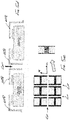
- FIG. 1a is a cross-sectional side view of a conventional WLP 100.
- the WLP 100 includes a plurality of input or output (I/O) pads 102 exposed on a bottom surface of the WLP 100.
- the I/O pads 102 are mounted to contacts 104, such as pads on a printed circuit board (PCB) with solder 106.
- PCB printed circuit board
- FIG. 1b is an enlarged schematic bottom plan view of a part 108 of the WLP 100 along line A-A of FIG. 1a .
- the bottom surface of the WLP 100 includes the I/O pad 102, which is a metal area, a saw scribe lane area 110 located at a peripheral area of the bottom surface of the WLP 100, which is a non-passivated area, and a passivation overlap area 112 located between the I/O pad 102 and the saw scribe lane area 110.
- the active pad 102 does not extend all the way to the sides of the WLP 100, once the WLP 100 is mounted to the PCB and the I/O pads 102 are soldered to the corresponding contact 104, it is difficult to inspect the solder joints to determine if there are any potential solder joint defects.
- a semiconductor device comprising: a semiconductor die having a top major surface that has one or more electrical contacts formed thereon, an opposing bottom major surface, and side surfaces; a molding material encapsulating the top major surface, the bottom major surface and the side surfaces of the semiconductor die, wherein the molding material defines a package body that has a top surface and a side surface; wherein the plurality of electrical contacts are exposed on the top surface of the package body and a metal layer is arranged over and electrically connected to the electrical contacts and wherein the metal layer extends to and at least partially covers a side surface of the package body.
- the metal layer may comprise copper and the metal layer may be coated with a wettable material, such as tin.
- the metal layer may extend across the width of the top surface of the package body.
- the molding material may be arranged unitarily to encapsulate to the semiconductor die.
- a method for assembling a semiconductor device may comprise: providing an plurality of spaced apart semiconductor dies, the semiconductor die having a top major surface with one or more electrical contacts formed thereon, an opposing bottom major surface and side surfaces, wherein each die has a plurality of electrical contacts formed on a top surface; encapsulating the dies with a molding material, wherein the molding material partially covers partially top surfaces such that the electrical contacts are exposed and covers the bottom surface and side surface of the dies; cutting a plurality of first trenches to defines a package body side wall of each semiconductor device; forming a metal layer over a top surface of each package body, wherein the metal layer electrically contacts the electrical contacts, and extends to the side surface of each package body; and singulating the semiconductor devices from each other.
- the metal layer may comprise copper and the metal layer may be formed by sputtering or plating.
- the metal layer may be coated with a wettable material by electro-plating. The metal layer may extend across the width of the top surface of the package body.
- moulding the semiconductor dies comprises unitarily to encapsulating each semiconductor die with a moulding material.
- the device 200 includes a semiconductor die 202 having a top major surface 204 and an opposing bottom major surface 208.
- the top major surface 204 of the semiconductor die 202 has one or more electrical contacts 206 formed thereon.
- the semiconductor die 202 may comprises one or more active components (not illustrated) such as transistors or diodes, and one or more electrical contacts 206.
- the electrical contacts may preferably be formed by depositing a patterned metal layer on the die top surface 204, to provide electrical connections to the one or more active components of the semiconductor die 202.
- the semiconductor device 200 also includes a molding material 210 that covers the bottom surface 208 and each of side the surfaces of the semiconductor die 202.
- the molding material 210 covers at least a part of the top surface 204 of the semiconductor die, wherein the contacts 204 arranged on the top surface 204 will be free from moulding material 210.
- the molding material 210 defines a package body that has a top surface 212, respective side surfaces 214 and a bottom surface 215. Where the electrical contacts 206 are free from moulding material 210, openings are defined in the top surface 212 of the package body such that the electrical contacts 206 are at least partially exposed through the openings in the moulding material 210. Depending on the moulding process used, the tops of the electrical contacts may be substantially level with the top of the moulding material 210. Alternatively, the tops of the contacts may be arranged to be below the top of the moulding material 210.
- the device 200 further includes a metal layer 218 formed over and electrically connected to the electrical contacts 206 through the openings 216. The metal layer 218 extends to and at least partially cover the side surface 214 of the package body.
- the metal layers 218, which are respectively electrically connected to the electrical contacts 206, are spaced and isolated from each other by a gap 220 located therebetween.
- the metal layers 218 form an intermetallic layer between the metallic electrical contacts 206 and I/O pads 222 (discussed below) of the semiconductor device 200.
- the metal layers 218 may comprise copper and the metal layer 218 is coated with a wettable material, such as tin, by a for example a plating process, to form the I/O pads 222 such that the device 200 has wettable flanks that allow for solder joint to be formed between the I/O pads 222 and the contact pads of a PCB.
- the metal layer 218 having the wettable material forms an I/O pad that allow for solder joint inspection by for example Automatic Optical Inspection, as required by automotive qualified semiconductor devices.
- the top surface 204 of the semiconductor die 202 with the exception of the location of the electrical contacts as discussed above, is covered with moulding material the packaged semiconductor die is protected on six sides by the moulding material.
- the chance of flux residues or solder flakes causing a short circuit between the I/O pads 102 and the semiconductor die 202 when mounting to a PCB is reduced.
- the arrangement as described above may result in a lower package height because there is no need for die carrier or mount.
- the I/O pads 222 may extend across the entire width of the of the top surface of the package body and also across the entire width of the side surfaces 214 of the package body.
- a carrier such as a PCB
- this arrangement of I/O pads 222 results in improved visibility of the solder joint connecting the I/O pad 222 to a contact pad of the PCB.
- the I/O pads 222 may extend partially across the width of the of the top surface of the package body and also partially across the width of the side surfaces 214 of the package body.
- the solder pad which is larger with same body width and the solder is very visible than option 3 b.
- FIGs 4a to 4e illustrate the steps in moulding the wafer level semiconductor device in accordance with an embodiment.
- Semiconductor dies 202 are initially singulated (not Illustrated) from a wafer containing an array of such semiconductor dies 202. As illustrated in Figure 4a , semiconductor dies 202 are mounted on a carrier tape 402. The semiconductor dies 202 are mounted by way of the electrical contacts 206 which are fixed to the carrier tape 402.
- the wafer containing an array of such semiconductor dies 202 may be mounted on a carrier tape 402.
- the semiconductor dies 202 may then be singulated, without cutting the carrier tape 402 such that they remain on the carrier tape 402 ready for moulding.
- the moulding process may be a film assisted moulding process whereby the 402 prevents moulding material 212 from covering the top surfaces of the electrical contacts 206. As discussed above this results in the top surface of the electrical contacts 206 being substantially level with the top surface of the mould material 212.
- Use of the carrier tape 402 also prevents moulding material 212 from covering the electrical contacts 206, such that the electrical contacts 206 are free from moulding material 212 as discussed above.
- using this method of moulding ensure at all six-sides of the semiconductor die, with the exception of the location of the electrical contacts is covered in a single step by a single unitarily formed moulding material 212.
- the moulded array of semiconductor dies 202 is then mounted on an a carrier 404 as illustrated in Figure 4d such that the electrical contacts 206 face upwards from the carrier.
- the carrier 404 may be any appropriate temporary carrier such as a film frame carrier (FFC), to hold the individual semiconductor devices 202 in place during singulation (as discussed below).
- FFC film frame carrier
- a partial cut is made into the moulding material 212 in a direction towards the FFC 404 as illustrated in Figure 4e .
- the cuts are made between adjacent sidewalls of adjacent semiconductor dies 202 in an array of such dies.
- the cut is partial in that it does not extend fully through the moulding material 212 and terminates prior to the FFC 404 thus forming trenches in the moulding material 212 and partially defining the side walls of the semiconductor device 200.
- the cuts may be made using any appropriate means such as a laser or a saw blade of appropriate kerf.
- a metal layer 406 is formed over the top surface, that is the surface having the electrical contacts 206 of each package body, such that the metal layer is electrically connected to the electrical contacts 206.
- the metal layer 406 also extends to the side surface of each package body and a bottom surface formed by the trenches cut in the moulding material.
- the metal layer 406 is formed by sputtering or plating and the metal layer 406 may comprise copper.
- the metal layer interlayer 406 may be removed from the top of the package between the contacts 206, in order to prevent a short circuit therebetween.
- the metal layer 406 may be removed by etching or cutting.
- the step of removing the metal interlayer layer 406 may expose the moulding material at the top of the package.
- the metal inter layer is coated with a wettable material 408 by electro-plating to complete formation of the I/O pads 222.
- the wettable material 440 may comprise tin.
- the electro-plating is performed prior to removal of the metal interlayer 406 between the contacts 206.
- singulation is performed along the trenches and between the remaining adjacent side walls to singulate the semiconductor devices 200 from each other.
- the singulation process is described in more detail with respect to Figure 5e .
- a partial cut is made through the moulding material 212 prior to formation of the I/O pads 222.
- a first cut is carried out through the moulding material 212 in the y-direction.
- a second cut is then carried out in the x-direction following the partial cut described above. This second cut may optionally be made with saw which has a smaller kerf than the kerf of the saw used for making the partial cut. This results in a stepped feature in the side wall of the moulding material.
Landscapes
- Structures Or Materials For Encapsulating Or Coating Semiconductor Devices Or Solid State Devices (AREA)
- Encapsulation Of And Coatings For Semiconductor Or Solid State Devices (AREA)
- Engineering & Computer Science (AREA)
- Manufacturing & Machinery (AREA)
Abstract
This disclosure relates to a semiconductor device structure and method of manufacturing a semiconductor device. The semiconductor device may comprise a semiconductor die having a top major surface that has one or more electrical contacts formed thereon, an opposing bottom major surface, and side surfaces; a molding material encapsulating the top major surface, the bottom major surface and the side surfaces of the semiconductor die, wherein the molding material defines a package body that has a top surface and a side surface; wherein the plurality of electrical contacts are exposed on the top surface of the package body and a metal layer is arranged over and electrically connected to the electrical contacts and wherein the metal layer extends to and at least partially covers a side surface of the package body.
Description
- The present disclosure relates to a semiconductor device and method of manufacture. More particularly the present disclosure relates to a wafer level semiconductor device with wettable side contacts.
- Semiconductor devices in the form of wafer level packages (WLP) are becoming increasingly important for applications that require a small device footprint with improved electrical performance. Wafer level packages are commonly used, for example, in portable electronic devices such as mobile communications devices.
-
FIG. 1a is a cross-sectional side view of aconventional WLP 100. The WLP 100 includes a plurality of input or output (I/O)pads 102 exposed on a bottom surface of theWLP 100. The I/O pads 102 are mounted tocontacts 104, such as pads on a printed circuit board (PCB) withsolder 106. -
FIG. 1b is an enlarged schematic bottom plan view of apart 108 of theWLP 100 along line A-A ofFIG. 1a . The bottom surface of the WLP 100 includes the I/O pad 102, which is a metal area, a sawscribe lane area 110 located at a peripheral area of the bottom surface of theWLP 100, which is a non-passivated area, and apassivation overlap area 112 located between the I/O pad 102 and the sawscribe lane area 110. - However, as shown in
FIG. 1b or excessive solder, together with a very narrow separation between the I/O pad 102 and the sawscribe lane area 110 can result in a flux residue orsolder flake 114 which may bridge theactive pad 102 and the saw scribedlane area 110, which can result in a short circuit between the I/O pads 102 and the die of theWLP 100. - In addition, because the
active pad 102 does not extend all the way to the sides of theWLP 100, once theWLP 100 is mounted to the PCB and the I/O pads 102 are soldered to thecorresponding contact 104, it is difficult to inspect the solder joints to determine if there are any potential solder joint defects. - According to an embodiment there is provided a semiconductor device comprising: a semiconductor die having a top major surface that has one or more electrical contacts formed thereon, an opposing bottom major surface, and side surfaces; a molding material encapsulating the top major surface, the bottom major surface and the side surfaces of the semiconductor die, wherein the molding material defines a package body that has a top surface and a side surface; wherein the plurality of electrical contacts are exposed on the top surface of the package body and a metal layer is arranged over and electrically connected to the electrical contacts and wherein the metal layer extends to and at least partially covers a side surface of the package body.
- Optionally, the metal layer may comprise copper and the metal layer may be coated with a wettable material, such as tin.
- Optionally, the metal layer may extend across the width of the top surface of the package body.
- Optionally, the molding material may be arranged unitarily to encapsulate to the semiconductor die.
- According to an embodiment there is provided a method for assembling a semiconductor device, the method may comprise: providing an plurality of spaced apart semiconductor dies, the semiconductor die having a top major surface with one or more electrical contacts formed thereon, an opposing bottom major surface and side surfaces, wherein each die has a plurality of electrical contacts formed on a top surface; encapsulating the dies with a molding material, wherein the molding material partially covers partially top surfaces such that the electrical contacts are exposed and covers the bottom surface and side surface of the dies; cutting a plurality of first trenches to defines a package body side wall of each semiconductor device; forming a metal layer over a top surface of each package body, wherein the metal layer electrically contacts the electrical contacts, and extends to the side surface of each package body; and singulating the semiconductor devices from each other.
- Optionally, the metal layer may comprise copper and the metal layer may be formed by sputtering or plating. Optionally, the metal layer may be coated with a wettable material by electro-plating. The metal layer may extend across the width of the top surface of the package body.
- Optionally, moulding the semiconductor dies comprises unitarily to encapsulating each semiconductor die with a moulding material.
- So that the manner in which the features of the present disclosure can be understood in detail, a more particular description is made with reference to embodiments, some of which are illustrated in the appended figures. It is to be noted, however, that the appended figures illustrate only typical embodiments and are therefore not to be considered limiting of its scope. The figures are for facilitating an understanding of the disclosure and thus are not necessarily drawn to scale. Advantages of the subject matter claimed will become apparent to those skilled in the art upon reading this description in conjunction with the accompanying figures, in which like reference numerals have been used to designate like elements, and in which:
-
Figure 1a shows a cross-sectional side view of a conventional wafer level semiconductor device; -
Figure 1b shows is an enlarged bottom plan view of the conventional wafer level semiconductor device ofFigure 1a taken along line A-A ofFigure 1a ; -
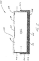
Figure 2 illustrates an a cross-sectional side view a wafer level semiconductor device in accordance with an embodiment; -
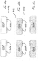
Figure 3a illustrates an isometric view of a wafer level semiconductor device in accordance with an embodiment; -
Figure 3b illustrates an isometric view of a wafer level semiconductor device in accordance with an embodiment; -
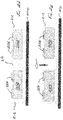
Figure 4a illustrates the step of mounting a semiconductor die on a carrier tape; -
Figure 4b illustrates the step of encapsulating the semiconductor die; -
Figure 4c illustrates the step of removing the carrier tape; -
Figure 4d illustrates the step of mounting the encapsulated semiconductor die on a temporary carrier; -
Figure 4e illustrates the step of partially singulating the semiconductor die; -
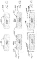
Figure 5a illustrates the formation of the metallic interlayer; -
Figure 5b illustrates the further formation of the metallic interlayer; -
Figure 5c illustrates the formation of formation of metallic I/O pads; -
Figure 5d illustrates singulation of the wafer level semiconductor devices according to embodiments; and -
Figure 5e illustrates a plan view of an array of wafer level semiconductor devices following singulation. - With reference to
Figure 2 , a cross section of an example waferlevel semiconductor device 200 in accordance with an embodiments is illustrated. Thedevice 200 includes asemiconductor die 202 having a topmajor surface 204 and an opposing bottommajor surface 208. The topmajor surface 204 of thesemiconductor die 202 has one or moreelectrical contacts 206 formed thereon. Thesemiconductor die 202 may comprises one or more active components (not illustrated) such as transistors or diodes, and one or moreelectrical contacts 206. The electrical contacts may preferably be formed by depositing a patterned metal layer on the dietop surface 204, to provide electrical connections to the one or more active components of thesemiconductor die 202. - The
semiconductor device 200 also includes amolding material 210 that covers thebottom surface 208 and each of side the surfaces of thesemiconductor die 202. In addition themolding material 210 covers at least a part of thetop surface 204 of the semiconductor die, wherein thecontacts 204 arranged on thetop surface 204 will be free from mouldingmaterial 210. - The
molding material 210 defines a package body that has atop surface 212,respective side surfaces 214 and abottom surface 215. Where theelectrical contacts 206 are free from mouldingmaterial 210, openings are defined in thetop surface 212 of the package body such that theelectrical contacts 206 are at least partially exposed through the openings in themoulding material 210. Depending on the moulding process used, the tops of the electrical contacts may be substantially level with the top of themoulding material 210. Alternatively, the tops of the contacts may be arranged to be below the top of themoulding material 210. Thedevice 200 further includes a metal layer 218 formed over and electrically connected to theelectrical contacts 206 through the openings 216. The metal layer 218 extends to and at least partially cover theside surface 214 of the package body. - The metal layers 218, which are respectively electrically connected to the
electrical contacts 206, are spaced and isolated from each other by agap 220 located therebetween. The metal layers 218 form an intermetallic layer between the metallicelectrical contacts 206 and I/O pads 222 (discussed below) of thesemiconductor device 200. - The metal layers 218 may comprise copper and the metal layer 218 is coated with a wettable material, such as tin, by a for example a plating process, to form the I/
O pads 222 such that thedevice 200 has wettable flanks that allow for solder joint to be formed between the I/O pads 222 and the contact pads of a PCB. The metal layer 218 having the wettable material forms an I/O pad that allow for solder joint inspection by for example Automatic Optical Inspection, as required by automotive qualified semiconductor devices. In addition, because thetop surface 204 of the semiconductor die 202, with the exception of the location of the electrical contacts as discussed above, is covered with moulding material the packaged semiconductor die is protected on six sides by the moulding material. As a result, the chance of flux residues or solder flakes causing a short circuit between the I/O pads 102 and the semiconductor die 202 when mounting to a PCB is reduced. Furthermore, the arrangement as described above may result in a lower package height because there is no need for die carrier or mount. - Referring to
Figure 3a , which illustrates an isometric view of thesemiconductor device 200 according to an embodiment, the I/O pads 222 may extend across the entire width of the of the top surface of the package body and also across the entire width of the side surfaces 214 of the package body. When thesemiconductor device 200 is mounted on a carrier, such as a PCB, this arrangement of I/O pads 222 results in improved visibility of the solder joint connecting the I/O pad 222 to a contact pad of the PCB. - In an alternative arrangement, as illustrated in
Figure 3b which illustrates an isometric view of thesemiconductor device 200 according to an embodiment, the I/O pads 222 may extend partially across the width of the of the top surface of the package body and also partially across the width of the side surfaces 214 of the package body. - Option 3a, the solder pad which is larger with same body width and the solder is very visible than option 3 b.
-
Figures 4a to 4e illustrate the steps in moulding the wafer level semiconductor device in accordance with an embodiment. Semiconductor dies 202 are initially singulated (not Illustrated) from a wafer containing an array of such semiconductor dies 202. As illustrated inFigure 4a , semiconductor dies 202 are mounted on acarrier tape 402. The semiconductor dies 202 are mounted by way of theelectrical contacts 206 which are fixed to thecarrier tape 402. - In an alternative process the wafer containing an array of such semiconductor dies 202 may be mounted on a
carrier tape 402. The semiconductor dies 202 may then be singulated, without cutting thecarrier tape 402 such that they remain on thecarrier tape 402 ready for moulding. - Following mounting of the semiconductor dies 202 on the
carrier tape 402 the semiconductor dies 202 are then moulded as illustrated inFigure 4b . The moulding process may be a film assisted moulding process whereby the 402 preventsmoulding material 212 from covering the top surfaces of theelectrical contacts 206. As discussed above this results in the top surface of theelectrical contacts 206 being substantially level with the top surface of themould material 212. Use of thecarrier tape 402 also preventsmoulding material 212 from covering theelectrical contacts 206, such that theelectrical contacts 206 are free frommoulding material 212 as discussed above. Furthermore, using this method of moulding ensure at all six-sides of the semiconductor die, with the exception of the location of the electrical contacts is covered in a single step by a single unitarily formedmoulding material 212. - Following removal of the
carrier tape 402 as illustrated inFigure 4c , the moulded array of semiconductor dies 202 is then mounted on an acarrier 404 as illustrated inFigure 4d such that theelectrical contacts 206 face upwards from the carrier. Thecarrier 404 may be any appropriate temporary carrier such as a film frame carrier (FFC), to hold theindividual semiconductor devices 202 in place during singulation (as discussed below). - Following mounting of the semiconductor dies 202 on the FFC 404 a partial cut is made into the
moulding material 212 in a direction towards theFFC 404 as illustrated inFigure 4e . The cuts are made between adjacent sidewalls of adjacent semiconductor dies 202 in an array of such dies. The cut is partial in that it does not extend fully through themoulding material 212 and terminates prior to theFFC 404 thus forming trenches in themoulding material 212 and partially defining the side walls of thesemiconductor device 200. The cuts may be made using any appropriate means such as a laser or a saw blade of appropriate kerf. - Following the above moulding and cutting steps the I/
O pads 222 are then formed as illustrated with reference toFigures 5a to 5d . As illustrated inFigure 5a , ametal layer 406 is formed over the top surface, that is the surface having theelectrical contacts 206 of each package body, such that the metal layer is electrically connected to theelectrical contacts 206. Themetal layer 406 also extends to the side surface of each package body and a bottom surface formed by the trenches cut in the moulding material. Optionally, themetal layer 406 is formed by sputtering or plating and themetal layer 406 may comprise copper. - As illustrated in
Figure 5b , themetal layer interlayer 406 may be removed from the top of the package between thecontacts 206, in order to prevent a short circuit therebetween. Themetal layer 406 may be removed by etching or cutting. The step of removing themetal interlayer layer 406 may expose the moulding material at the top of the package. Following formation of themetal interlayer 406 and as illustrated inFigure 5c the metal inter layer is coated with awettable material 408 by electro-plating to complete formation of the I/O pads 222. The wettable material 440 may comprise tin. Optionally, the electro-plating is performed prior to removal of themetal interlayer 406 between thecontacts 206. - As illustrated in
Figure 5d singulation is performed along the trenches and between the remaining adjacent side walls to singulate thesemiconductor devices 200 from each other. The singulation process is described in more detail with respect toFigure 5e . As discussed above with respect toFigure 4e a partial cut is made through themoulding material 212 prior to formation of the I/O pads 222. Following formation of the I/O pads 222 a first cut is carried out through themoulding material 212 in the y-direction. A second cut is then carried out in the x-direction following the partial cut described above. This second cut may optionally be made with saw which has a smaller kerf than the kerf of the saw used for making the partial cut. This results in a stepped feature in the side wall of the moulding material. - Whilst the above examples illustrate two I/
O pads 222, the skilled person will see that based on the above discussion any number or arrangement may be achieved without departing from the scope of the present disclosure. In this way, the skilled person will see that the above example may be applicable to for example dual silicon no-lead (DSN) arrangements. - Particular and preferred aspects of the invention are set out in the accompanying independent claims. Combinations of features from the dependent and/or independent claims may be combined as appropriate and not merely as set out in the claims.
- The scope of the present disclosure includes any novel feature or combination of features disclosed therein either explicitly or implicitly or any generalisation thereof irrespective of whether or not it relates to the claimed invention or mitigate against any or all of the problems addressed by the present invention. The applicant hereby gives notice that new claims may be formulated to such features during prosecution of this application or of any such further application derived there from. In particular, with reference to the appended claims, features from dependent claims may be combined with those of the independent claims and features from respective independent claims may be combined in any appropriate manner and not merely in specific combinations enumerated in the claims.
- Features which are described in the context of separate embodiments may also be provided in combination in a single embodiment. Conversely, various features which are, for brevity, described in the context of a single embodiment, may also be provided separately or in any suitable sub combination.
- Term "comprising" does not exclude other elements or steps, the term "a" or "an" does not exclude a plurality. Reference signs in the claims shall not be construed as limiting the scope of the claims.
Claims (12)
- A semiconductor device, comprising:a semiconductor die having a top major surface that has one or more electrical contacts formed thereon, an opposing bottom major surface, and side surfaces;a molding material encapsulating the top major surface, the bottom major surface and the side surfaces of the semiconductor die, wherein the molding material defines a package body that has a top surface and a side surface;wherein the plurality of electrical contacts are exposed on the top surface of the package body and a metal layer is arranged over and electrically connected to the electrical contacts and wherein the metal layer extends to and at least partially covers a side surface of the package body.
- The semiconductor device of claim 1, wherein the metal layer comprises copper.
- The semiconductor device of claims 1 to 2, wherein the metal layer is coated with a wettable material.
- The semiconductor device of claim 3, wherein the wettable material comprises tin.
- The semiconductor device of claims 1 to 4, wherein the metal layer extends across the width of the top surface of the package body.
- The semiconductor device of claims 1 to 5, wherein the molding material is arranged unitarily to encapsulate to the semiconductor die.
- A method for assembling a semiconductor device, the method comprising:providing an plurality of spaced apart semiconductor dies, the semiconductor die having a top major surface with one or more electrical contacts formed thereon, an opposing bottom major surface and side surfaces, wherein each die has a plurality of electrical contacts formed on a top surface;encapsulating the dies with a molding material, wherein the molding material partially covers partially top surfaces such that the electrical contacts are exposed and covers the bottom surface and side surface of the dies;cutting a plurality of first trenches to defines a package body side wall of each semiconductor device; forming a metal layer over a top surface of each package body, wherein the metal layer electrically contacts the electrical contacts, and extends to the side surface of each package body; andsingulating the semiconductor devices from each other.
- The method of claim 7 wherein the metal layer comprises copper.
- The method of claim 7 to 8 wherein the metal layer is formed by sputtering or plating.
- The method of claims 7 to 9 further comprising coating the metal layer with a wettable material by electro-plating.
- The method of claims 7 to 10, wherein the metal layer extends across the width of the top surface of the package body.
- The method of claims 7 to 11, wherein the moulding the semiconductor dies comprises unitarily to encapsulating each semiconductor die with a moulding material.
Priority Applications (4)
| Application Number | Priority Date | Filing Date | Title |
|---|---|---|---|
| EP17207326.4A EP3499552A1 (en) | 2017-12-14 | 2017-12-14 | Semiconductor device and method of manufacture |
| CN202411608207.7A CN119447068A (en) | 2017-12-14 | 2018-12-11 | Semiconductor device and manufacturing method |
| CN201811510321.0A CN109979902A (en) | 2017-12-14 | 2018-12-11 | Semiconductor device and manufacturing method |
| US16/220,125 US11094562B2 (en) | 2017-12-14 | 2018-12-14 | Semiconductor device and method of manufacture |
Applications Claiming Priority (1)
| Application Number | Priority Date | Filing Date | Title |
|---|---|---|---|
| EP17207326.4A EP3499552A1 (en) | 2017-12-14 | 2017-12-14 | Semiconductor device and method of manufacture |
Publications (1)
| Publication Number | Publication Date |
|---|---|
| EP3499552A1 true EP3499552A1 (en) | 2019-06-19 |
Family
ID=60923228
Family Applications (1)
| Application Number | Title | Priority Date | Filing Date |
|---|---|---|---|
| EP17207326.4A Withdrawn EP3499552A1 (en) | 2017-12-14 | 2017-12-14 | Semiconductor device and method of manufacture |
Country Status (3)
| Country | Link |
|---|---|
| US (1) | US11094562B2 (en) |
| EP (1) | EP3499552A1 (en) |
| CN (2) | CN119447068A (en) |
Families Citing this family (2)
| Publication number | Priority date | Publication date | Assignee | Title |
|---|---|---|---|---|
| CN114914161A (en) * | 2022-05-23 | 2022-08-16 | 常州银河世纪微电子股份有限公司 | Chip size packaging process |
| US12315773B2 (en) | 2022-05-23 | 2025-05-27 | Changzhou Galaxy Century Microelectronics Co., Ltd | Chip scale package (CSP) process |
Citations (5)
| Publication number | Priority date | Publication date | Assignee | Title |
|---|---|---|---|---|
| US5656863A (en) * | 1993-02-18 | 1997-08-12 | Mitsubishi Denki Kabushiki Kaisha | Resin seal semiconductor package |
| US20060197187A1 (en) * | 2005-01-28 | 2006-09-07 | Infineon Technologies Ag | Semiconductor device and method for producing same |
| US20070170577A1 (en) * | 2006-01-26 | 2007-07-26 | Infineon Technologies Ag | Semiconductor Device with Surface-Mountable External Contacts and Method for Manufacturing the Same |
| US20140264888A1 (en) * | 2013-03-12 | 2014-09-18 | Inpaq Technology Co., Ltd. | Semiconductor package structure and method of manufacturing the same |
| CN106816424A (en) * | 2015-12-01 | 2017-06-09 | 安世有限公司 | Electronic component and its manufacture method, the lead frame for the electronic component |
Family Cites Families (30)
| Publication number | Priority date | Publication date | Assignee | Title |
|---|---|---|---|---|
| JPS59185801U (en) * | 1983-05-26 | 1984-12-10 | アルプス電気株式会社 | chip resistance |
| US4792781A (en) * | 1986-02-21 | 1988-12-20 | Tdk Corporation | Chip-type resistor |
| AU2659995A (en) * | 1994-06-09 | 1996-01-04 | Chipscale, Inc. | Resistor fabrication |
| JPH09260568A (en) * | 1996-03-27 | 1997-10-03 | Mitsubishi Electric Corp | Semiconductor device and manufacturing method thereof |
| JPH09260538A (en) * | 1996-03-27 | 1997-10-03 | Miyazaki Oki Electric Co Ltd | Resin-sealed semiconductor device, manufacturing method, and mounting structure thereof |
| US6285085B1 (en) * | 1997-08-13 | 2001-09-04 | Citizen Watch Co., Ltd. | Semiconductor device, method of fabricating the same and structure for mounting the same |
| US5888884A (en) * | 1998-01-02 | 1999-03-30 | General Electric Company | Electronic device pad relocation, precision placement, and packaging in arrays |
| KR100315030B1 (en) * | 1998-12-29 | 2002-04-24 | 박종섭 | Manufacturing method of semiconductor package |
| KR20000057810A (en) * | 1999-01-28 | 2000-09-25 | 가나이 쓰토무 | Semiconductor device |
| US6337510B1 (en) * | 2000-11-17 | 2002-01-08 | Walsin Advanced Electronics Ltd | Stackable QFN semiconductor package |
| SG120879A1 (en) * | 2002-08-08 | 2006-04-26 | Micron Technology Inc | Packaged microelectronic components |
| JP4173751B2 (en) * | 2003-02-28 | 2008-10-29 | 株式会社ルネサステクノロジ | Semiconductor device |
| KR100585100B1 (en) * | 2003-08-23 | 2006-05-30 | 삼성전자주식회사 | Thin semiconductor package having a stackable lead frame and manufacturing method thereof |
| US7368810B2 (en) * | 2003-08-29 | 2008-05-06 | Micron Technology, Inc. | Invertible microfeature device packages |
| DE10351028B4 (en) * | 2003-10-31 | 2005-09-08 | Infineon Technologies Ag | Semiconductor component and suitable manufacturing / assembly process |
| JP3910598B2 (en) * | 2004-03-04 | 2007-04-25 | 松下電器産業株式会社 | Resin-sealed semiconductor device and manufacturing method thereof |
| US7385299B2 (en) * | 2006-02-25 | 2008-06-10 | Stats Chippac Ltd. | Stackable integrated circuit package system with multiple interconnect interface |
| EP2390909A1 (en) * | 2010-05-24 | 2011-11-30 | Jerry Hu | Miniature packaging for discrete circuit components |
| US9406646B2 (en) * | 2011-10-27 | 2016-08-02 | Infineon Technologies Ag | Electronic device and method for fabricating an electronic device |
| KR101959395B1 (en) * | 2012-07-06 | 2019-03-18 | 삼성전자주식회사 | Semiconductor Devices and Methods of Fabricating the Same |
| TWI549243B (en) * | 2013-03-07 | 2016-09-11 | 精材科技股份有限公司 | Semiconductor structure and method of manufacturing same |
| TWI560828B (en) * | 2014-02-11 | 2016-12-01 | Xintex Inc | Chip package and method for forming the same |
| TWI560829B (en) * | 2014-03-07 | 2016-12-01 | Xintec Inc | Chip package and method thereof |
| US10211172B2 (en) * | 2014-03-13 | 2019-02-19 | Maxim Integrated Products, Inc. | Wafer-based electronic component packaging |
| TWI546913B (en) * | 2014-04-02 | 2016-08-21 | 精材科技股份有限公司 | Chip package and method of manufacturing same |
| US9390993B2 (en) * | 2014-08-15 | 2016-07-12 | Broadcom Corporation | Semiconductor border protection sealant |
| US9978720B2 (en) * | 2015-07-06 | 2018-05-22 | Infineon Technologies Ag | Insulated die |
| EP3168870A1 (en) * | 2015-11-11 | 2017-05-17 | Nexperia B.V. | Semiconductor device and method of making a semiconductor device |
| US9837375B2 (en) * | 2016-02-26 | 2017-12-05 | Semtech Corporation | Semiconductor device and method of forming insulating layers around semiconductor die |
| US10276510B2 (en) * | 2017-09-25 | 2019-04-30 | Powertech Technology Inc. | Manufacturing method of package structure having conductive shield |
-
2017
- 2017-12-14 EP EP17207326.4A patent/EP3499552A1/en not_active Withdrawn
-
2018
- 2018-12-11 CN CN202411608207.7A patent/CN119447068A/en active Pending
- 2018-12-11 CN CN201811510321.0A patent/CN109979902A/en active Pending
- 2018-12-14 US US16/220,125 patent/US11094562B2/en active Active
Patent Citations (5)
| Publication number | Priority date | Publication date | Assignee | Title |
|---|---|---|---|---|
| US5656863A (en) * | 1993-02-18 | 1997-08-12 | Mitsubishi Denki Kabushiki Kaisha | Resin seal semiconductor package |
| US20060197187A1 (en) * | 2005-01-28 | 2006-09-07 | Infineon Technologies Ag | Semiconductor device and method for producing same |
| US20070170577A1 (en) * | 2006-01-26 | 2007-07-26 | Infineon Technologies Ag | Semiconductor Device with Surface-Mountable External Contacts and Method for Manufacturing the Same |
| US20140264888A1 (en) * | 2013-03-12 | 2014-09-18 | Inpaq Technology Co., Ltd. | Semiconductor package structure and method of manufacturing the same |
| CN106816424A (en) * | 2015-12-01 | 2017-06-09 | 安世有限公司 | Electronic component and its manufacture method, the lead frame for the electronic component |
Also Published As
| Publication number | Publication date |
|---|---|
| CN109979902A (en) | 2019-07-05 |
| CN119447068A (en) | 2025-02-14 |
| US11094562B2 (en) | 2021-08-17 |
| US20190189468A1 (en) | 2019-06-20 |
Similar Documents
| Publication | Publication Date | Title |
|---|---|---|
| US10410941B2 (en) | Wafer level semiconductor device with wettable flanks | |
| US7745261B2 (en) | Chip scale package fabrication methods | |
| US7087462B1 (en) | Method for forming leadless semiconductor packages | |
| KR100727519B1 (en) | Semiconductor device packaged into chip size and manufacturing method thereof | |
| US8163601B2 (en) | Chip-exposed semiconductor device and its packaging method | |
| US8766408B2 (en) | Semiconductor device and manufacturing method thereof | |
| CN1288256A (en) | Semiconductor device chip scale surface assembling and packaging, and mfg. method therefor | |
| US10211129B2 (en) | Process for manufacturing a surface-mount semiconductor device having exposed solder material | |
| KR20150009668A (en) | Semiconductor device package and method for manufacturing the same | |
| US11764075B2 (en) | Package assembly for plating with selective molding | |
| US7777311B2 (en) | Circuit substrate, molding semiconductor device, tray and inspection socket | |
| CN107112245A (en) | QFN encapsulation with improved contact pin | |
| US11094562B2 (en) | Semiconductor device and method of manufacture | |
| CN102468194A (en) | Semiconductor device packaging method and semiconductor device package | |
| US11715714B2 (en) | Semiconductor devices and methods of manufacturing semiconductor devices | |
| US6919624B2 (en) | Semiconductor device with exposed electrodes | |
| CN119601473A (en) | Chip packaging method and chip packaging structure | |
| KR100871379B1 (en) | Manufacturing method of semiconductor package | |
| US20220344175A1 (en) | Flip chip package unit and associated packaging method | |
| TWI868735B (en) | Electronic package module and method for fabricating the same | |
| KR102340866B1 (en) | Semiconductor package and a method of manufacturing the same | |
| CN119108355A (en) | Electronic packaging module and manufacturing method thereof | |
| US20250062217A1 (en) | Packaged semiconductor device and method of manufacturing | |
| JP2008171962A (en) | Semiconductor device and manufacturing method of semiconductor device | |
| HK1057648B (en) | Chip scale surface mounted device and process of manufacture |
Legal Events
| Date | Code | Title | Description |
|---|---|---|---|
| PUAI | Public reference made under article 153(3) epc to a published international application that has entered the european phase |
Free format text: ORIGINAL CODE: 0009012 |
|
| AK | Designated contracting states |
Kind code of ref document: A1 Designated state(s): AL AT BE BG CH CY CZ DE DK EE ES FI FR GB GR HR HU IE IS IT LI LT LU LV MC MK MT NL NO PL PT RO RS SE SI SK SM TR |
|
| AX | Request for extension of the european patent |
Extension state: BA ME |
|
| STAA | Information on the status of an ep patent application or granted ep patent |
Free format text: STATUS: THE APPLICATION IS DEEMED TO BE WITHDRAWN |
|
| 18D | Application deemed to be withdrawn |
Effective date: 20191220 |