EP3499305A1 - Array substrate and liquid crystal display panel - Google Patents
Array substrate and liquid crystal display panel Download PDFInfo
- Publication number
- EP3499305A1 EP3499305A1 EP16912468.2A EP16912468A EP3499305A1 EP 3499305 A1 EP3499305 A1 EP 3499305A1 EP 16912468 A EP16912468 A EP 16912468A EP 3499305 A1 EP3499305 A1 EP 3499305A1
- Authority
- EP
- European Patent Office
- Prior art keywords
- array substrate
- layer
- thin film
- film transistors
- liquid crystal
- Prior art date
- Legal status (The legal status is an assumption and is not a legal conclusion. Google has not performed a legal analysis and makes no representation as to the accuracy of the status listed.)
- Granted
Links
Images

Classifications
-
- G—PHYSICS
- G02—OPTICS
- G02F—OPTICAL DEVICES OR ARRANGEMENTS FOR THE CONTROL OF LIGHT BY MODIFICATION OF THE OPTICAL PROPERTIES OF THE MEDIA OF THE ELEMENTS INVOLVED THEREIN; NON-LINEAR OPTICS; FREQUENCY-CHANGING OF LIGHT; OPTICAL LOGIC ELEMENTS; OPTICAL ANALOGUE/DIGITAL CONVERTERS
- G02F1/00—Devices or arrangements for the control of the intensity, colour, phase, polarisation or direction of light arriving from an independent light source, e.g. switching, gating or modulating; Non-linear optics
- G02F1/01—Devices or arrangements for the control of the intensity, colour, phase, polarisation or direction of light arriving from an independent light source, e.g. switching, gating or modulating; Non-linear optics for the control of the intensity, phase, polarisation or colour
- G02F1/13—Devices or arrangements for the control of the intensity, colour, phase, polarisation or direction of light arriving from an independent light source, e.g. switching, gating or modulating; Non-linear optics for the control of the intensity, phase, polarisation or colour based on liquid crystals, e.g. single liquid crystal display cells
- G02F1/133—Constructional arrangements; Operation of liquid crystal cells; Circuit arrangements
- G02F1/1333—Constructional arrangements; Manufacturing methods
- G02F1/133345—Insulating layers
-
- G—PHYSICS
- G02—OPTICS
- G02F—OPTICAL DEVICES OR ARRANGEMENTS FOR THE CONTROL OF LIGHT BY MODIFICATION OF THE OPTICAL PROPERTIES OF THE MEDIA OF THE ELEMENTS INVOLVED THEREIN; NON-LINEAR OPTICS; FREQUENCY-CHANGING OF LIGHT; OPTICAL LOGIC ELEMENTS; OPTICAL ANALOGUE/DIGITAL CONVERTERS
- G02F1/00—Devices or arrangements for the control of the intensity, colour, phase, polarisation or direction of light arriving from an independent light source, e.g. switching, gating or modulating; Non-linear optics
- G02F1/01—Devices or arrangements for the control of the intensity, colour, phase, polarisation or direction of light arriving from an independent light source, e.g. switching, gating or modulating; Non-linear optics for the control of the intensity, phase, polarisation or colour
- G02F1/13—Devices or arrangements for the control of the intensity, colour, phase, polarisation or direction of light arriving from an independent light source, e.g. switching, gating or modulating; Non-linear optics for the control of the intensity, phase, polarisation or colour based on liquid crystals, e.g. single liquid crystal display cells
- G02F1/133—Constructional arrangements; Operation of liquid crystal cells; Circuit arrangements
- G02F1/1333—Constructional arrangements; Manufacturing methods
- G02F1/13338—Input devices, e.g. touch panels
-
- G—PHYSICS
- G02—OPTICS
- G02F—OPTICAL DEVICES OR ARRANGEMENTS FOR THE CONTROL OF LIGHT BY MODIFICATION OF THE OPTICAL PROPERTIES OF THE MEDIA OF THE ELEMENTS INVOLVED THEREIN; NON-LINEAR OPTICS; FREQUENCY-CHANGING OF LIGHT; OPTICAL LOGIC ELEMENTS; OPTICAL ANALOGUE/DIGITAL CONVERTERS
- G02F1/00—Devices or arrangements for the control of the intensity, colour, phase, polarisation or direction of light arriving from an independent light source, e.g. switching, gating or modulating; Non-linear optics
- G02F1/01—Devices or arrangements for the control of the intensity, colour, phase, polarisation or direction of light arriving from an independent light source, e.g. switching, gating or modulating; Non-linear optics for the control of the intensity, phase, polarisation or colour
- G02F1/13—Devices or arrangements for the control of the intensity, colour, phase, polarisation or direction of light arriving from an independent light source, e.g. switching, gating or modulating; Non-linear optics for the control of the intensity, phase, polarisation or colour based on liquid crystals, e.g. single liquid crystal display cells
- G02F1/133—Constructional arrangements; Operation of liquid crystal cells; Circuit arrangements
- G02F1/1333—Constructional arrangements; Manufacturing methods
- G02F1/1335—Structural association of cells with optical devices, e.g. polarisers or reflectors
- G02F1/133509—Filters, e.g. light shielding masks
- G02F1/133514—Colour filters
-
- G—PHYSICS
- G02—OPTICS
- G02F—OPTICAL DEVICES OR ARRANGEMENTS FOR THE CONTROL OF LIGHT BY MODIFICATION OF THE OPTICAL PROPERTIES OF THE MEDIA OF THE ELEMENTS INVOLVED THEREIN; NON-LINEAR OPTICS; FREQUENCY-CHANGING OF LIGHT; OPTICAL LOGIC ELEMENTS; OPTICAL ANALOGUE/DIGITAL CONVERTERS
- G02F1/00—Devices or arrangements for the control of the intensity, colour, phase, polarisation or direction of light arriving from an independent light source, e.g. switching, gating or modulating; Non-linear optics
- G02F1/01—Devices or arrangements for the control of the intensity, colour, phase, polarisation or direction of light arriving from an independent light source, e.g. switching, gating or modulating; Non-linear optics for the control of the intensity, phase, polarisation or colour
- G02F1/13—Devices or arrangements for the control of the intensity, colour, phase, polarisation or direction of light arriving from an independent light source, e.g. switching, gating or modulating; Non-linear optics for the control of the intensity, phase, polarisation or colour based on liquid crystals, e.g. single liquid crystal display cells
- G02F1/133—Constructional arrangements; Operation of liquid crystal cells; Circuit arrangements
- G02F1/1333—Constructional arrangements; Manufacturing methods
- G02F1/1339—Gaskets; Spacers; Sealing of cells
- G02F1/13394—Gaskets; Spacers; Sealing of cells spacers regularly patterned on the cell subtrate, e.g. walls, pillars
-
- G—PHYSICS
- G02—OPTICS
- G02F—OPTICAL DEVICES OR ARRANGEMENTS FOR THE CONTROL OF LIGHT BY MODIFICATION OF THE OPTICAL PROPERTIES OF THE MEDIA OF THE ELEMENTS INVOLVED THEREIN; NON-LINEAR OPTICS; FREQUENCY-CHANGING OF LIGHT; OPTICAL LOGIC ELEMENTS; OPTICAL ANALOGUE/DIGITAL CONVERTERS
- G02F1/00—Devices or arrangements for the control of the intensity, colour, phase, polarisation or direction of light arriving from an independent light source, e.g. switching, gating or modulating; Non-linear optics
- G02F1/01—Devices or arrangements for the control of the intensity, colour, phase, polarisation or direction of light arriving from an independent light source, e.g. switching, gating or modulating; Non-linear optics for the control of the intensity, phase, polarisation or colour
- G02F1/13—Devices or arrangements for the control of the intensity, colour, phase, polarisation or direction of light arriving from an independent light source, e.g. switching, gating or modulating; Non-linear optics for the control of the intensity, phase, polarisation or colour based on liquid crystals, e.g. single liquid crystal display cells
- G02F1/133—Constructional arrangements; Operation of liquid crystal cells; Circuit arrangements
- G02F1/1333—Constructional arrangements; Manufacturing methods
- G02F1/1343—Electrodes
- G02F1/13439—Electrodes characterised by their electrical, optical, physical properties; materials therefor; method of making
-
- G—PHYSICS
- G02—OPTICS
- G02F—OPTICAL DEVICES OR ARRANGEMENTS FOR THE CONTROL OF LIGHT BY MODIFICATION OF THE OPTICAL PROPERTIES OF THE MEDIA OF THE ELEMENTS INVOLVED THEREIN; NON-LINEAR OPTICS; FREQUENCY-CHANGING OF LIGHT; OPTICAL LOGIC ELEMENTS; OPTICAL ANALOGUE/DIGITAL CONVERTERS
- G02F1/00—Devices or arrangements for the control of the intensity, colour, phase, polarisation or direction of light arriving from an independent light source, e.g. switching, gating or modulating; Non-linear optics
- G02F1/01—Devices or arrangements for the control of the intensity, colour, phase, polarisation or direction of light arriving from an independent light source, e.g. switching, gating or modulating; Non-linear optics for the control of the intensity, phase, polarisation or colour
- G02F1/13—Devices or arrangements for the control of the intensity, colour, phase, polarisation or direction of light arriving from an independent light source, e.g. switching, gating or modulating; Non-linear optics for the control of the intensity, phase, polarisation or colour based on liquid crystals, e.g. single liquid crystal display cells
- G02F1/133—Constructional arrangements; Operation of liquid crystal cells; Circuit arrangements
- G02F1/136—Liquid crystal cells structurally associated with a semi-conducting layer or substrate, e.g. cells forming part of an integrated circuit
- G02F1/1362—Active matrix addressed cells
- G02F1/136227—Through-hole connection of the pixel electrode to the active element through an insulation layer
-
- G—PHYSICS
- G02—OPTICS
- G02F—OPTICAL DEVICES OR ARRANGEMENTS FOR THE CONTROL OF LIGHT BY MODIFICATION OF THE OPTICAL PROPERTIES OF THE MEDIA OF THE ELEMENTS INVOLVED THEREIN; NON-LINEAR OPTICS; FREQUENCY-CHANGING OF LIGHT; OPTICAL LOGIC ELEMENTS; OPTICAL ANALOGUE/DIGITAL CONVERTERS
- G02F1/00—Devices or arrangements for the control of the intensity, colour, phase, polarisation or direction of light arriving from an independent light source, e.g. switching, gating or modulating; Non-linear optics
- G02F1/01—Devices or arrangements for the control of the intensity, colour, phase, polarisation or direction of light arriving from an independent light source, e.g. switching, gating or modulating; Non-linear optics for the control of the intensity, phase, polarisation or colour
- G02F1/13—Devices or arrangements for the control of the intensity, colour, phase, polarisation or direction of light arriving from an independent light source, e.g. switching, gating or modulating; Non-linear optics for the control of the intensity, phase, polarisation or colour based on liquid crystals, e.g. single liquid crystal display cells
- G02F1/133—Constructional arrangements; Operation of liquid crystal cells; Circuit arrangements
- G02F1/136—Liquid crystal cells structurally associated with a semi-conducting layer or substrate, e.g. cells forming part of an integrated circuit
- G02F1/1362—Active matrix addressed cells
- G02F1/136286—Wiring, e.g. gate line, drain line
-
- G—PHYSICS
- G02—OPTICS
- G02F—OPTICAL DEVICES OR ARRANGEMENTS FOR THE CONTROL OF LIGHT BY MODIFICATION OF THE OPTICAL PROPERTIES OF THE MEDIA OF THE ELEMENTS INVOLVED THEREIN; NON-LINEAR OPTICS; FREQUENCY-CHANGING OF LIGHT; OPTICAL LOGIC ELEMENTS; OPTICAL ANALOGUE/DIGITAL CONVERTERS
- G02F1/00—Devices or arrangements for the control of the intensity, colour, phase, polarisation or direction of light arriving from an independent light source, e.g. switching, gating or modulating; Non-linear optics
- G02F1/01—Devices or arrangements for the control of the intensity, colour, phase, polarisation or direction of light arriving from an independent light source, e.g. switching, gating or modulating; Non-linear optics for the control of the intensity, phase, polarisation or colour
- G02F1/13—Devices or arrangements for the control of the intensity, colour, phase, polarisation or direction of light arriving from an independent light source, e.g. switching, gating or modulating; Non-linear optics for the control of the intensity, phase, polarisation or colour based on liquid crystals, e.g. single liquid crystal display cells
- G02F1/133—Constructional arrangements; Operation of liquid crystal cells; Circuit arrangements
- G02F1/136—Liquid crystal cells structurally associated with a semi-conducting layer or substrate, e.g. cells forming part of an integrated circuit
- G02F1/1362—Active matrix addressed cells
- G02F1/1368—Active matrix addressed cells in which the switching element is a three-electrode device
-
- H—ELECTRICITY
- H10—SEMICONDUCTOR DEVICES; ELECTRIC SOLID-STATE DEVICES NOT OTHERWISE PROVIDED FOR
- H10D—INORGANIC ELECTRIC SEMICONDUCTOR DEVICES
- H10D86/00—Integrated devices formed in or on insulating or conducting substrates, e.g. formed in silicon-on-insulator [SOI] substrates or on stainless steel or glass substrates
- H10D86/40—Integrated devices formed in or on insulating or conducting substrates, e.g. formed in silicon-on-insulator [SOI] substrates or on stainless steel or glass substrates characterised by multiple TFTs
- H10D86/441—Interconnections, e.g. scanning lines
-
- H—ELECTRICITY
- H10—SEMICONDUCTOR DEVICES; ELECTRIC SOLID-STATE DEVICES NOT OTHERWISE PROVIDED FOR
- H10D—INORGANIC ELECTRIC SEMICONDUCTOR DEVICES
- H10D86/00—Integrated devices formed in or on insulating or conducting substrates, e.g. formed in silicon-on-insulator [SOI] substrates or on stainless steel or glass substrates
- H10D86/40—Integrated devices formed in or on insulating or conducting substrates, e.g. formed in silicon-on-insulator [SOI] substrates or on stainless steel or glass substrates characterised by multiple TFTs
- H10D86/451—Integrated devices formed in or on insulating or conducting substrates, e.g. formed in silicon-on-insulator [SOI] substrates or on stainless steel or glass substrates characterised by multiple TFTs characterised by the compositions or shapes of the interlayer dielectrics
-
- H—ELECTRICITY
- H10—SEMICONDUCTOR DEVICES; ELECTRIC SOLID-STATE DEVICES NOT OTHERWISE PROVIDED FOR
- H10D—INORGANIC ELECTRIC SEMICONDUCTOR DEVICES
- H10D86/00—Integrated devices formed in or on insulating or conducting substrates, e.g. formed in silicon-on-insulator [SOI] substrates or on stainless steel or glass substrates
- H10D86/40—Integrated devices formed in or on insulating or conducting substrates, e.g. formed in silicon-on-insulator [SOI] substrates or on stainless steel or glass substrates characterised by multiple TFTs
- H10D86/481—Integrated devices formed in or on insulating or conducting substrates, e.g. formed in silicon-on-insulator [SOI] substrates or on stainless steel or glass substrates characterised by multiple TFTs integrated with passive devices, e.g. auxiliary capacitors
-
- H—ELECTRICITY
- H10—SEMICONDUCTOR DEVICES; ELECTRIC SOLID-STATE DEVICES NOT OTHERWISE PROVIDED FOR
- H10D—INORGANIC ELECTRIC SEMICONDUCTOR DEVICES
- H10D86/00—Integrated devices formed in or on insulating or conducting substrates, e.g. formed in silicon-on-insulator [SOI] substrates or on stainless steel or glass substrates
- H10D86/40—Integrated devices formed in or on insulating or conducting substrates, e.g. formed in silicon-on-insulator [SOI] substrates or on stainless steel or glass substrates characterised by multiple TFTs
- H10D86/60—Integrated devices formed in or on insulating or conducting substrates, e.g. formed in silicon-on-insulator [SOI] substrates or on stainless steel or glass substrates characterised by multiple TFTs wherein the TFTs are in active matrices
-
- G—PHYSICS
- G02—OPTICS
- G02F—OPTICAL DEVICES OR ARRANGEMENTS FOR THE CONTROL OF LIGHT BY MODIFICATION OF THE OPTICAL PROPERTIES OF THE MEDIA OF THE ELEMENTS INVOLVED THEREIN; NON-LINEAR OPTICS; FREQUENCY-CHANGING OF LIGHT; OPTICAL LOGIC ELEMENTS; OPTICAL ANALOGUE/DIGITAL CONVERTERS
- G02F1/00—Devices or arrangements for the control of the intensity, colour, phase, polarisation or direction of light arriving from an independent light source, e.g. switching, gating or modulating; Non-linear optics
- G02F1/01—Devices or arrangements for the control of the intensity, colour, phase, polarisation or direction of light arriving from an independent light source, e.g. switching, gating or modulating; Non-linear optics for the control of the intensity, phase, polarisation or colour
- G02F1/13—Devices or arrangements for the control of the intensity, colour, phase, polarisation or direction of light arriving from an independent light source, e.g. switching, gating or modulating; Non-linear optics for the control of the intensity, phase, polarisation or colour based on liquid crystals, e.g. single liquid crystal display cells
- G02F1/133—Constructional arrangements; Operation of liquid crystal cells; Circuit arrangements
- G02F1/136—Liquid crystal cells structurally associated with a semi-conducting layer or substrate, e.g. cells forming part of an integrated circuit
- G02F1/1362—Active matrix addressed cells
- G02F1/136213—Storage capacitors associated with the pixel electrode
-
- G—PHYSICS
- G02—OPTICS
- G02F—OPTICAL DEVICES OR ARRANGEMENTS FOR THE CONTROL OF LIGHT BY MODIFICATION OF THE OPTICAL PROPERTIES OF THE MEDIA OF THE ELEMENTS INVOLVED THEREIN; NON-LINEAR OPTICS; FREQUENCY-CHANGING OF LIGHT; OPTICAL LOGIC ELEMENTS; OPTICAL ANALOGUE/DIGITAL CONVERTERS
- G02F2202/00—Materials and properties
- G02F2202/10—Materials and properties semiconductor
- G02F2202/104—Materials and properties semiconductor poly-Si
Definitions
- the present disclosure relates to a liquid crystal display technology field, and more particularly to an array substrate and a liquid crystal display panel.
- the bottom of PS 11 is blocked by the BM 13, the bottom of the data line 14 is also blocked by the BM 13.
- the PS is easily to slide in the left and right sides of the PLN hole, resulting in PS ratio too small, insufficient support and related adverse.
- the bottom of the PS 11 in the dashed box 15 is also blocked by the BM 13, losing the aperture ratio.
- the embodiment of the present disclosure provides an array substrate and a liquid crystal display panel, can prevent the PS sliding in the hole of the organic transparent layer, it is possible to increase the stability of the PS.
- the present disclosure provides an array substrate, thin film transistors are arranged matrix on the array substrate, a first passivation layer is arranged on the source/drain electrode of the thin film transistors, an organic transparent layer is arranged on the first passivation layer and is located in an area other than the area of the thin film transistors and the area between the adjacent two thin film transistors, post spacers are arranged on the surface of the array substrate, and is located between any two of the thin film transistors.
- the array substrate further includes a first ITO layer arranged on the organic transparent layer, the first ITO layer, the first passivation layer and the second metal layer form the storage capacitor, wherein the second metal layer is arranged in the same layer with the source/drain electrode of the thin film transistors, a first metal layer forms the scan line of the array substrate.
- the array substrate further includes a second passivation layer arranged on the first ITO layer.
- the post spacers are arranged on the second passivation layer.
- the array substrate further includes a second ITO layer arranged on the second passivation layer, the second ITO layer forms the pixel electrode.
- the pixel electrode is connected with the source/drain electrode of the thin film transistors through a via hole.
- the post spacers are arranged between the adjacent two via holes on the source/drain electrode of the thin film transistors.
- the touch metal layer and the touch insulating layer are sequentially arranged between the organic transparent layer and the first ITO layer.
- the array substrate may be a non-touch array substrate, may also be an in-cell touch array substrate.
- the present disclosure provides a liquid crystal display panel, includes: a color film substrate, an array substrate, liquid crystal and post spacers sandwiched between the color film substrate and the array substrate; thin film transistors are arranged matrix on the array substrate, a first passivation layer is arranged on the source/drain electrode of the thin film transistors, an organic transparent layer is arranged on the first passivation layer and is located in an area other than the area of the thin film transistors and the area between the adjacent two thin film transistors, post spacers are arranged on the surface of the array substrate, and is located between any two of the thin film transistors.
- the array substrate further includes a first ITO layer arranged on the organic transparent layer, the first ITO layer, the first passivation layer and a second metal layer form a storage capacitor, wherein the second metal layer is arranged in the same layer with the source/drain electrode of the thin film transistors, a first metal layer forms the scan line of the array substrate.
- the array substrate further includes a second passivation layer arranged on the first ITO layer.
- the post spacers are arranged on the second passivation layer.
- the array substrate further includes a second ITO layer arranged on the second passivation layer, the second ITO layer forms the pixel electrode.
- the pixel electrode is connected with the source/drain electrode of the thin film transistors through a via hole.
- the post spacers are arranged between the adjacent two via holes on the source/drain electrode of the thin film transistors.
- a touch metal layer and a touch insulating layer are sequentially arranged between the organic transparent layer and the first ITO layer.
- the array substrate may be a non-touch array substrate, may also be an in-cell touch array substrate.
- the beneficial effects of the present disclosure is: thin film transistors are arranged matrix on the array substrate of the present disclosure, the first passivation layer is arranged on the source/drain electrode of the thin film transistors, the organic transparent layer is arranged on the first passivation layer, and is located in an area other than the area of the thin film transistors and the area between the adjacent two thin film transistors, post spacers are arranged on the surface of the array substrate, and is located between any two of the thin film transistors, can prevent the PS sliding in the hole of the organic transparent layer and increase the stability of the PS.
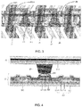
- FIG. 3 is a structure schematic diagram of the liquid crystal display panel of the embodiment of the present disclosure.
- FIG. 4 is a sectional schematic diagram corresponding to FIG. 3 .
- the liquid crystal display panel of the embodiment of the present disclosure includes: a color film substrate 21, an array substrate 22, liquid crystal sandwiched between the color film substrate 21 and the array substrate 22 (not shown) and a post spacer 23.
- thin film transistors 221 are arranged matrix on the array substrate 22 of the embodiment of the present disclosure
- the first passivation layer 222 is arranged on the source/drain electrode 223 of the thin film transistors 221
- the organic transparent layer (not shown) is arranged on the first passivation layer 222, and is located in an area other than the area of the thin film transistors 221 and the area between the adjacent two thin film transistors 221
- post spacers 23 are arranged on the surface of the array substrate 22, and is located between any two of the thin film transistors 221.
- the organic transparent layer is whole digging a hole along the gate electrode direction of the thin film transistors 221 to form a hole 24, so that when arranging the post spacer 23 between any two of the thin film transistors 221, improving the PS slide in the hole of the organic transparent layer by group the color film substrate 21 and the array substrate 22 or overlay bad, making the stability of the group of the color film substrate 21 and the array substrate 22 higher.
- the array substrate 22 further includes a first ITO layer 224 arranged on the organic transparent layer.
- the organic transparent layer is whole digging a hole along the thin film transistor 221 in the area of the thin film transistor 221 and the area between adjacent two thin film transistors 221 and the first ITO layer 224 is directly arranged on the second metal layer 225 in the area.
- the first ITO layer 224, the first passivation layer 222 and the second metal layer 225 form the storage capacitor.
- the second metal layer 225 and the source/drain electrode of the thin film transistor 221 are arranged in the same layer, and forming the data line 25, the first metal layer is formed the scan line 26 of the array substrate 22.
- the array substrate 22 further includes the second passivation layer 226 arranged on the first ITO layer 224.
- the PS 23 is arranged on the second passivation layer 226.
- the array substrate 22 further includes the second ITO layer 227 arranged on the second passivation layer 226, the second ITO layer 227 forms the pixel electrode 27.
- the pixel electrode 27 is connected with the source/drain electrode 223 of the thin film transistor 221 through a via hole 28.
- the gate electrode of the thin film transistor 221 is formed by a polysilicon layer 228, between the polysilicon layer 228 and the source/drain electrode 223 further arranged the gate insulating layer 229 and the dielectric layer 2210.
- the array substrate 22 may be a non-touch array substrate, refer to FIG. 3 and FIG. 4 ; may also be an in-cell touch array substrate.
- the in-cell touch array substrate between the organic transparent layer and the first ITO layer sequentially arranged the touch metal layer and touch insulating layer, other structure is as same as the non-touch array substrate structure, not discussed here.
- the non-touch array substrate may be applied to a non-touch liquid crystal display panel, may also be applied to a liquid crystal display panel additionally provided with the touch panel.
- the black matrix 210 at the position corresponding to the post spacer 23 in the color film substrate 21 to block the dark line caused the liquid crystal disorder by the poor alignment.
- the position corresponding to the scan line 26 and the data line 25 is further arranged the black matrix 210.
- the upper and lower bottom surface of the post spacer 23 is hexagon, side of the post spacer 23 is trapezoid structure.
- the post spacer 23 is arranged between the adjacent two via holes 28 on the source/drain electrode 223 of the thin film transistor 221. I.e. the surface 231 of the post spacer 23 contacted with the array substrate 22 is between the adjacent two via holes 28 on the source/drain electrode 223 of the thin film transistor 221.
- the present disclosure has thin film transistor arranged on the array substrate, the first passivation layer is arranged on the source/drain electrode of the thin film transistor, the organic transparent layer is arranged on the first passivation layer and is located in an area other than the area of the thin film transistors and the area between the adjacent two thin film transistors, post spacers are arranged on the surface of the array substrate, and is located between any two of the thin film transistors, can prevent the PS sliding in the hole of the organic transparent layer, it is possible to increase the stability of the PS.
Landscapes
- Physics & Mathematics (AREA)
- Nonlinear Science (AREA)
- Mathematical Physics (AREA)
- Chemical & Material Sciences (AREA)
- Crystallography & Structural Chemistry (AREA)
- General Physics & Mathematics (AREA)
- Optics & Photonics (AREA)
- Engineering & Computer Science (AREA)
- Microelectronics & Electronic Packaging (AREA)
- Power Engineering (AREA)
- Liquid Crystal (AREA)
- Devices For Indicating Variable Information By Combining Individual Elements (AREA)
Abstract
Description
- The present disclosure relates to a liquid crystal display technology field, and more particularly to an array substrate and a liquid crystal display panel.
- With the demand of the liquid crystal panel, high aperture ratio and high resolution (Pixel Per Inch, PPI) became the important goals of the panel design. With the higher PPI, the pixel size is smaller. Due to the height of the post spacer (PS), whether it is photo alignment or rubbing alignment, the height makes the alignment with some blind area, therefore the bottom of the PS needs to use the black matrix (BM) to block the dark line caused the liquid crystal disorder by the poor alignment. Thus, as should not affect the aperture ratio, the position of the PS in the Pixel is very critical. Generally, we choose the PS standing in the middle of two thin film transistors (TFT), refer to
FIG. 1 , thePS 11 is arranged between the two holes of the organic transparent insulating layer (PLN) 12. The bottom ofPS 11 is blocked by theBM 13, the bottom of thedata line 14 is also blocked by theBM 13. In the generally design, after group the TFT and the CF, since the pixel size is small to allow narrowing the range of the precision to the group, the PS is easily to slide in the left and right sides of the PLN hole, resulting in PS ratio too small, insufficient support and related adverse. InFIG. 2 , although move up thePS 11 may avoid the hole of thePLN 12, the bottom of thePS 11 in thedashed box 15 is also blocked by theBM 13, losing the aperture ratio. - The embodiment of the present disclosure provides an array substrate and a liquid crystal display panel, can prevent the PS sliding in the hole of the organic transparent layer, it is possible to increase the stability of the PS.
- The present disclosure provides an array substrate, thin film transistors are arranged matrix on the array substrate, a first passivation layer is arranged on the source/drain electrode of the thin film transistors, an organic transparent layer is arranged on the first passivation layer and is located in an area other than the area of the thin film transistors and the area between the adjacent two thin film transistors, post spacers are arranged on the surface of the array substrate, and is located between any two of the thin film transistors.
- Wherein, the array substrate further includes a first ITO layer arranged on the organic transparent layer, the first ITO layer, the first passivation layer and the second metal layer form the storage capacitor, wherein the second metal layer is arranged in the same layer with the source/drain electrode of the thin film transistors, a first metal layer forms the scan line of the array substrate.
- Wherein, the array substrate further includes a second passivation layer arranged on the first ITO layer.
- Wherein, the post spacers are arranged on the second passivation layer.
- Wherein, the array substrate further includes a second ITO layer arranged on the second passivation layer, the second ITO layer forms the pixel electrode.
- Wherein, the pixel electrode is connected with the source/drain electrode of the thin film transistors through a via hole.
- Wherein, the post spacers are arranged between the adjacent two via holes on the source/drain electrode of the thin film transistors.
- Wherein, the touch metal layer and the touch insulating layer are sequentially arranged between the organic transparent layer and the first ITO layer.
- Wherein, the array substrate may be a non-touch array substrate, may also be an in-cell touch array substrate.
- The present disclosure provides a liquid crystal display panel, includes: a color film substrate, an array substrate, liquid crystal and post spacers sandwiched between the color film substrate and the array substrate; thin film transistors are arranged matrix on the array substrate, a first passivation layer is arranged on the source/drain electrode of the thin film transistors, an organic transparent layer is arranged on the first passivation layer and is located in an area other than the area of the thin film transistors and the area between the adjacent two thin film transistors, post spacers are arranged on the surface of the array substrate, and is located between any two of the thin film transistors.
- Wherein, the array substrate further includes a first ITO layer arranged on the organic transparent layer, the first ITO layer, the first passivation layer and a second metal layer form a storage capacitor, wherein the second metal layer is arranged in the same layer with the source/drain electrode of the thin film transistors, a first metal layer forms the scan line of the array substrate.
- Wherein, the array substrate further includes a second passivation layer arranged on the first ITO layer.
- Wherein, the post spacers are arranged on the second passivation layer.
- Wherein, the array substrate further includes a second ITO layer arranged on the second passivation layer, the second ITO layer forms the pixel electrode.
- Wherein, the pixel electrode is connected with the source/drain electrode of the thin film transistors through a via hole.
- Wherein, the post spacers are arranged between the adjacent two via holes on the source/drain electrode of the thin film transistors.
- Wherein, a touch metal layer and a touch insulating layer are sequentially arranged between the organic transparent layer and the first ITO layer.
- Wherein, the array substrate may be a non-touch array substrate, may also be an in-cell touch array substrate.
- By the above method, the beneficial effects of the present disclosure is: thin film transistors are arranged matrix on the array substrate of the present disclosure, the first passivation layer is arranged on the source/drain electrode of the thin film transistors, the organic transparent layer is arranged on the first passivation layer, and is located in an area other than the area of the thin film transistors and the area between the adjacent two thin film transistors, post spacers are arranged on the surface of the array substrate, and is located between any two of the thin film transistors, can prevent the PS sliding in the hole of the organic transparent layer and increase the stability of the PS.
- In order to more clearly illustrate the embodiments or the prior art technical solutions embodiment of the present disclosure, it will implement the following figures for the cases described in the prior art or the need to use a simple introduction. Apparently, the following description the drawings are only some embodiments of the present disclosure, those of ordinary skill in speaking, without creative efforts of the premise, you can also obtain other drawings based on these drawings. Wherein:
-
FIG. 1 is a structure schematic diagram of the liquid crystal display panel of the prior art; -
FIG. 2 is a structure schematic diagram of another liquid crystal display panel of the prior art; -
FIG. 3 is a structure schematic diagram of the liquid crystal display panel of the embodiment of the present disclosure; -
FIG. 4 is a sectional schematic diagram of the liquid crystal display panel of the embodiment of the present disclosure. - The present disclosure will now be combined with the implementation of the accompanying drawings, were clear examples of technical solutions of the present disclosure, fully described, it is clear that the described embodiments are merely part of the embodiments of the present disclosure, but not all embodiments Example. Based on the embodiments of the present disclosure, those of ordinary skill in not making all other embodiments without creative efforts obtained, are within the scope of the present disclosure is protected.
- Refer to
FIG. 3 and FIG. 4, FIG. 3 is a structure schematic diagram of the liquid crystal display panel of the embodiment of the present disclosure.FIG. 4 is a sectional schematic diagram corresponding toFIG. 3 . The liquid crystal display panel of the embodiment of the present disclosure includes: acolor film substrate 21, anarray substrate 22, liquid crystal sandwiched between thecolor film substrate 21 and the array substrate 22 (not shown) and apost spacer 23. - Refer to
FIG. 3 and FIG. 4 ,thin film transistors 221 are arranged matrix on thearray substrate 22 of the embodiment of the present disclosure, thefirst passivation layer 222 is arranged on the source/drain electrode 223 of thethin film transistors 221, the organic transparent layer (not shown) is arranged on thefirst passivation layer 222, and is located in an area other than the area of thethin film transistors 221 and the area between the adjacent twothin film transistors 221,post spacers 23 are arranged on the surface of thearray substrate 22, and is located between any two of thethin film transistors 221. In the embodiment of the present disclosure, the organic transparent layer is whole digging a hole along the gate electrode direction of thethin film transistors 221 to form ahole 24, so that when arranging thepost spacer 23 between any two of thethin film transistors 221, improving the PS slide in the hole of the organic transparent layer by group thecolor film substrate 21 and thearray substrate 22 or overlay bad, making the stability of the group of thecolor film substrate 21 and thearray substrate 22 higher. - In the embodiment of the present disclosure, the
array substrate 22 further includes afirst ITO layer 224 arranged on the organic transparent layer. The organic transparent layer is whole digging a hole along thethin film transistor 221 in the area of thethin film transistor 221 and the area between adjacent twothin film transistors 221 and thefirst ITO layer 224 is directly arranged on thesecond metal layer 225 in the area. Thefirst ITO layer 224, thefirst passivation layer 222 and thesecond metal layer 225 form the storage capacitor. Wherein, thesecond metal layer 225 and the source/drain electrode of thethin film transistor 221 are arranged in the same layer, and forming thedata line 25, the first metal layer is formed thescan line 26 of thearray substrate 22. - The
array substrate 22 further includes thesecond passivation layer 226 arranged on thefirst ITO layer 224. ThePS 23 is arranged on thesecond passivation layer 226. Thearray substrate 22 further includes thesecond ITO layer 227 arranged on thesecond passivation layer 226, thesecond ITO layer 227 forms thepixel electrode 27. Thepixel electrode 27 is connected with the source/drain electrode 223 of thethin film transistor 221 through avia hole 28. - In the embodiment of the present disclosure, the gate electrode of the
thin film transistor 221 is formed by apolysilicon layer 228, between thepolysilicon layer 228 and the source/drain electrode 223 further arranged thegate insulating layer 229 and thedielectric layer 2210. - In the embodiment of the present disclosure, the
array substrate 22 may be a non-touch array substrate, refer toFIG. 3 and FIG. 4 ; may also be an in-cell touch array substrate. In the in-cell touch array substrate, between the organic transparent layer and the first ITO layer sequentially arranged the touch metal layer and touch insulating layer, other structure is as same as the non-touch array substrate structure, not discussed here. It should be noted, the non-touch array substrate may be applied to a non-touch liquid crystal display panel, may also be applied to a liquid crystal display panel additionally provided with the touch panel. - In the liquid crystal display panel of the embodiment of the present disclosure, arranging the
black matrix 210 at the position corresponding to thepost spacer 23 in thecolor film substrate 21 to block the dark line caused the liquid crystal disorder by the poor alignment. In addition, the position corresponding to thescan line 26 and thedata line 25 is further arranged theblack matrix 210. - In the embodiment of the present disclosure, the upper and lower bottom surface of the
post spacer 23 is hexagon, side of thepost spacer 23 is trapezoid structure. Thepost spacer 23 is arranged between the adjacent two viaholes 28 on the source/drain electrode 223 of thethin film transistor 221. I.e. thesurface 231 of thepost spacer 23 contacted with thearray substrate 22 is between the adjacent two viaholes 28 on the source/drain electrode 223 of thethin film transistor 221. Can be seen fromFIG. 3 , thesurface 232 of thepost spacer 23 contacted with thecolor film substrate 21 without departing from the scope of theblack matrix 210 covered, description the designedpost spacer 23 does not affect the aperture ratio. - In summary, the present disclosure has thin film transistor arranged on the array substrate, the first passivation layer is arranged on the source/drain electrode of the thin film transistor, the organic transparent layer is arranged on the first passivation layer and is located in an area other than the area of the thin film transistors and the area between the adjacent two thin film transistors, post spacers are arranged on the surface of the array substrate, and is located between any two of the thin film transistors, can prevent the PS sliding in the hole of the organic transparent layer, it is possible to increase the stability of the PS.
- Above are only embodiments of the present disclosure is not patented and therefore limit the scope of the disclosure, all the contents of the present disclosure utilize the specification made equivalent structures or equivalent process transformation, either directly or indirectly related technologies used in other areas are included in the patent empathy scope of the disclosure.
Claims (18)
- An array substrate, wherein, thin film transistors are arranged matrix on the array substrate, a first passivation layer is arranged on the source/drain electrode of the thin film transistors, an organic transparent layer is arranged on the first passivation layer and is located in an area other than the area of the thin film transistors and the area between the adjacent two thin film transistors, post spacers are arranged on the surface of the array substrate, and is located between any two of the thin film transistors.
- The array substrate according to claim 1, wherein, the array substrate further comprises a first ITO layer arranged on the organic transparent layer, the first ITO layer, the first passivation layer and a second metal layer form a storage capacitor, wherein the second metal layer is arranged in the same layer with the source/drain electrode of the thin film transistors, a first metal layer forms the scan line of the array substrate.
- The array substrate according to claim 2, wherein, the array substrate further comprises a second passivation layer arranged on the first ITO layer.
- The array substrate according to claim 3, wherein, the post spacers are arranged on the second passivation layer.
- The array substrate according to claim 3, wherein, the array substrate further comprises a second ITO layer arranged on the second passivation layer, the second ITO layer forms a pixel electrode.
- The array substrate according to claim 5, wherein, the pixel electrode is connected with the source/drain electrode of the thin film transistors through a via hole.
- The array substrate according to claim 6, wherein, the post spacers are arranged between the adjacent two via holes on the source/drain electrode of the thin film transistors.
- The array substrate according to claim 2, wherein, a touch metal layer and a touch insulating layer are sequentially arranged between the organic transparent layer and the first ITO layer.
- The array substrate according to claim 1, wherein, the array substrate may be a non-touch array substrate, may also be an in-cell touch array substrate.
- A liquid crystal display panel, wherein, the liquid crystal display panel comprises: a color film substrate, an array substrate, liquid crystal and post spacers sandwiched between the color film substrate and the array substrate; thin film transistors are arranged matrix on the array substrate, a first passivation layer is arranged on the source/drain electrode of the thin film transistors, an organic transparent layer is arranged on the first passivation layer and is located in an area other than the area of the thin film transistors and the area between the adjacent two thin film transistors, post spacers are arranged on the surface of the array substrate, and is located between any two of the thin film transistors.
- The liquid crystal display panel according to claim 10, wherein, the array substrate further comprises a first ITO layer arranged on the organic transparent layer, the first ITO layer, the first passivation layer and a second metal layer form a storage capacitor, wherein the second metal layer is arranged in the same layer with the source/drain electrode of the thin film transistors, a first metal layer forms the scan line of the array substrate.
- The liquid crystal display panel according to claim 11, wherein, the array substrate further comprises a second passivation layer arranged on the first ITO layer.
- The liquid crystal display panel according to claim 12, wherein, the post spacers are arranged on the second passivation layer.
- The liquid crystal display panel according to claim 12, wherein, the array substrate further comprises a second ITO layer arranged on the second passivation layer, the second ITO layer forms a pixel electrode.
- The liquid crystal display panel according to claim 14, wherein, the pixel electrode is connected with the source/drain electrode of the thin film transistors through a via hole.
- The liquid crystal display panel according to claim 15, wherein, the post spacers are arranged between the adjacent two via holes on the source/drain electrode of the thin film transistors.
- The liquid crystal display panel according to claim 11, wherein, a touch metal layer and a touch insulating layer are sequentially arranged between the organic transparent layer and the first ITO layer.
- The liquid crystal display panel according to claim 10, wherein, the array substrate may be a non-touch array substrate, may also be an in-cell touch array substrate.
Applications Claiming Priority (2)
| Application Number | Priority Date | Filing Date | Title |
|---|---|---|---|
| CN201610643307.2A CN106094357B (en) | 2016-08-08 | 2016-08-08 | array substrate and liquid crystal display panel |
| PCT/CN2016/098171 WO2018028013A1 (en) | 2016-08-08 | 2016-09-06 | Array substrate and liquid crystal display panel |
Publications (3)
| Publication Number | Publication Date |
|---|---|
| EP3499305A1 true EP3499305A1 (en) | 2019-06-19 |
| EP3499305A4 EP3499305A4 (en) | 2020-01-22 |
| EP3499305B1 EP3499305B1 (en) | 2023-06-14 |
Family
ID=57454227
Family Applications (1)
| Application Number | Title | Priority Date | Filing Date |
|---|---|---|---|
| EP16912468.2A Active EP3499305B1 (en) | 2016-08-08 | 2016-09-06 | Array substrate and liquid crystal display panel |
Country Status (6)
| Country | Link |
|---|---|
| US (1) | US10295878B2 (en) |
| EP (1) | EP3499305B1 (en) |
| JP (1) | JP2019527854A (en) |
| KR (1) | KR102177646B1 (en) |
| CN (1) | CN106094357B (en) |
| WO (1) | WO2018028013A1 (en) |
Families Citing this family (2)
| Publication number | Priority date | Publication date | Assignee | Title |
|---|---|---|---|---|
| KR102661122B1 (en) * | 2016-11-21 | 2024-04-26 | 삼성디스플레이 주식회사 | Display device and method for fabricating the same |
| KR102825393B1 (en) | 2020-02-18 | 2025-06-25 | 주식회사 엘지화학 | Pattern film, transmission variable device comprising same and manufacturing method of transmission variable device |
Family Cites Families (13)
| Publication number | Priority date | Publication date | Assignee | Title |
|---|---|---|---|---|
| JP2003066488A (en) * | 2001-08-30 | 2003-03-05 | Hitachi Ltd | Liquid crystal display |
| KR100895306B1 (en) | 2002-11-14 | 2009-05-07 | 삼성전자주식회사 | Substrate for Liquid Crystal Display |
| KR101012494B1 (en) * | 2003-04-04 | 2011-02-08 | 엘지디스플레이 주식회사 | Reflective type liquid crystal display device |
| US9052550B2 (en) * | 2006-11-29 | 2015-06-09 | Beijing Boe Optoelectronics Technology Co., Ltd | Thin film transistor liquid crystal display |
| JP5278777B2 (en) * | 2010-11-09 | 2013-09-04 | Nltテクノロジー株式会社 | Liquid crystal display |
| JP5844072B2 (en) * | 2011-06-09 | 2016-01-13 | 株式会社ジャパンディスプレイ | Liquid crystal display |
| CN202141876U (en) * | 2011-07-05 | 2012-02-08 | 北京京东方光电科技有限公司 | Thin film transistor array substrate, liquid crystal display panel and liquid crystal display device |
| JP6002478B2 (en) * | 2012-07-04 | 2016-10-05 | 株式会社ジャパンディスプレイ | Liquid crystal display |
| JP2015118193A (en) * | 2013-12-18 | 2015-06-25 | 株式会社ジャパンディスプレイ | Liquid crystal display device |
| CN204269996U (en) | 2014-12-04 | 2015-04-15 | 厦门天马微电子有限公司 | LCD panel |
| KR101712246B1 (en) * | 2014-12-05 | 2017-03-06 | 엘지디스플레이 주식회사 | Self-capacitive touch sensor integrated type display device |
| CN105487718B (en) | 2016-01-29 | 2019-03-15 | 武汉华星光电技术有限公司 | Array substrate and manufacturing method thereof |
| US10811981B2 (en) | 2018-01-25 | 2020-10-20 | Nxp B.V. | Apparatus and method for a dual output resonant converter to ensure full power range for both outputs |
-
2016
- 2016-08-08 CN CN201610643307.2A patent/CN106094357B/en active Active
- 2016-09-06 JP JP2019505054A patent/JP2019527854A/en active Pending
- 2016-09-06 EP EP16912468.2A patent/EP3499305B1/en active Active
- 2016-09-06 WO PCT/CN2016/098171 patent/WO2018028013A1/en not_active Ceased
- 2016-09-06 US US15/128,394 patent/US10295878B2/en active Active
- 2016-09-06 KR KR1020197006978A patent/KR102177646B1/en active Active
Also Published As
| Publication number | Publication date |
|---|---|
| CN106094357A (en) | 2016-11-09 |
| WO2018028013A1 (en) | 2018-02-15 |
| KR20190034334A (en) | 2019-04-01 |
| EP3499305A4 (en) | 2020-01-22 |
| CN106094357B (en) | 2019-01-04 |
| EP3499305B1 (en) | 2023-06-14 |
| US10295878B2 (en) | 2019-05-21 |
| JP2019527854A (en) | 2019-10-03 |
| KR102177646B1 (en) | 2020-11-12 |
| US20180217428A1 (en) | 2018-08-02 |
Similar Documents
| Publication | Publication Date | Title |
|---|---|---|
| US10146078B2 (en) | Liquid crystal display panel and array substrate of the same | |
| US10886303B2 (en) | Array substrate with stepped groove and display device | |
| US8253905B2 (en) | Liquid crystal display device and method of making the same | |
| US10180601B2 (en) | Liquid crystal display panel and liquid crystal display apparatus | |
| US10197870B2 (en) | Array substrate and display device | |
| US12055830B2 (en) | Array substrate and liquid crystal display panel | |
| CN113311624A (en) | Array substrate and display panel | |
| US20250389994A1 (en) | Array substrate, manufacturing method thereof, and display panel | |
| KR20200022017A (en) | Integrated touch screen | |
| WO2019100430A1 (en) | Tft array substrate, production method and liquid crystal display panel | |
| US9841639B2 (en) | Touch display panel and fabrication method thereof, and display device | |
| US10802348B2 (en) | Array substrate, display panel and display device | |
| US10295878B2 (en) | Array substrate and liquid crystal display panel | |
| US20180039143A1 (en) | Liquid Crystal Display Panel, TFT Substrate And Manufacturing Method For The Same | |
| US20140145197A1 (en) | Pixel Structure, Dual Gate Pixel Structure And Display Device | |
| US20130141657A1 (en) | Array Substrate, Liquid Crystal Display Device and Manufacturing Method of Array Substrate | |
| US9780127B2 (en) | Liquid crystral display and manufacturing method thereof | |
| US8976329B2 (en) | Array substrate and LCD panel | |
| US9927645B2 (en) | Curved display device | |
| CN102393588B (en) | Display panel | |
| US20160154286A1 (en) | Liquid crystal display device and method of manufacturing the same | |
| KR20210012194A (en) | Thin film transistor and display device comprising the same | |
| US20210341805A1 (en) | Liquid crystal display panel, color film substrate, and thin film transistor substrate | |
| US20180348559A1 (en) | Array substrate, liquid crystal display panel, and liquid crystal display device | |
| CN117492280A (en) | Display panels and display devices |
Legal Events
| Date | Code | Title | Description |
|---|---|---|---|
| STAA | Information on the status of an ep patent application or granted ep patent |
Free format text: STATUS: THE INTERNATIONAL PUBLICATION HAS BEEN MADE |
|
| PUAI | Public reference made under article 153(3) epc to a published international application that has entered the european phase |
Free format text: ORIGINAL CODE: 0009012 |
|
| STAA | Information on the status of an ep patent application or granted ep patent |
Free format text: STATUS: REQUEST FOR EXAMINATION WAS MADE |
|
| 17P | Request for examination filed |
Effective date: 20190228 |
|
| AK | Designated contracting states |
Kind code of ref document: A1 Designated state(s): AL AT BE BG CH CY CZ DE DK EE ES FI FR GB GR HR HU IE IS IT LI LT LU LV MC MK MT NL NO PL PT RO RS SE SI SK SM TR |
|
| AX | Request for extension of the european patent |
Extension state: BA ME |
|
| DAV | Request for validation of the european patent (deleted) | ||
| DAX | Request for extension of the european patent (deleted) | ||
| A4 | Supplementary search report drawn up and despatched |
Effective date: 20191220 |
|
| RIC1 | Information provided on ipc code assigned before grant |
Ipc: G02F 1/1339 20060101AFI20191216BHEP Ipc: G02F 1/1362 20060101ALI20191216BHEP |
|
| STAA | Information on the status of an ep patent application or granted ep patent |
Free format text: STATUS: EXAMINATION IS IN PROGRESS |
|
| 17Q | First examination report despatched |
Effective date: 20210323 |
|
| GRAP | Despatch of communication of intention to grant a patent |
Free format text: ORIGINAL CODE: EPIDOSNIGR1 |
|
| STAA | Information on the status of an ep patent application or granted ep patent |
Free format text: STATUS: GRANT OF PATENT IS INTENDED |
|
| INTG | Intention to grant announced |
Effective date: 20230110 |
|
| GRAS | Grant fee paid |
Free format text: ORIGINAL CODE: EPIDOSNIGR3 |
|
| GRAA | (expected) grant |
Free format text: ORIGINAL CODE: 0009210 |
|
| STAA | Information on the status of an ep patent application or granted ep patent |
Free format text: STATUS: THE PATENT HAS BEEN GRANTED |
|
| AK | Designated contracting states |
Kind code of ref document: B1 Designated state(s): AL AT BE BG CH CY CZ DE DK EE ES FI FR GB GR HR HU IE IS IT LI LT LU LV MC MK MT NL NO PL PT RO RS SE SI SK SM TR |
|
| REG | Reference to a national code |
Ref country code: CH Ref legal event code: EP |
|
| REG | Reference to a national code |
Ref country code: DE Ref legal event code: R096 Ref document number: 602016080404 Country of ref document: DE |
|
| P01 | Opt-out of the competence of the unified patent court (upc) registered |
Effective date: 20230530 |
|
| REG | Reference to a national code |
Ref country code: AT Ref legal event code: REF Ref document number: 1579655 Country of ref document: AT Kind code of ref document: T Effective date: 20230715 |
|
| REG | Reference to a national code |
Ref country code: LT Ref legal event code: MG9D |
|
| REG | Reference to a national code |
Ref country code: NL Ref legal event code: MP Effective date: 20230614 |
|
| PG25 | Lapsed in a contracting state [announced via postgrant information from national office to epo] |
Ref country code: SE Free format text: LAPSE BECAUSE OF FAILURE TO SUBMIT A TRANSLATION OF THE DESCRIPTION OR TO PAY THE FEE WITHIN THE PRESCRIBED TIME-LIMIT Effective date: 20230614 Ref country code: NO Free format text: LAPSE BECAUSE OF FAILURE TO SUBMIT A TRANSLATION OF THE DESCRIPTION OR TO PAY THE FEE WITHIN THE PRESCRIBED TIME-LIMIT Effective date: 20230914 Ref country code: ES Free format text: LAPSE BECAUSE OF FAILURE TO SUBMIT A TRANSLATION OF THE DESCRIPTION OR TO PAY THE FEE WITHIN THE PRESCRIBED TIME-LIMIT Effective date: 20230614 |
|
| REG | Reference to a national code |
Ref country code: AT Ref legal event code: MK05 Ref document number: 1579655 Country of ref document: AT Kind code of ref document: T Effective date: 20230614 |
|
| PG25 | Lapsed in a contracting state [announced via postgrant information from national office to epo] |
Ref country code: RS Free format text: LAPSE BECAUSE OF FAILURE TO SUBMIT A TRANSLATION OF THE DESCRIPTION OR TO PAY THE FEE WITHIN THE PRESCRIBED TIME-LIMIT Effective date: 20230614 Ref country code: NL Free format text: LAPSE BECAUSE OF FAILURE TO SUBMIT A TRANSLATION OF THE DESCRIPTION OR TO PAY THE FEE WITHIN THE PRESCRIBED TIME-LIMIT Effective date: 20230614 Ref country code: LV Free format text: LAPSE BECAUSE OF FAILURE TO SUBMIT A TRANSLATION OF THE DESCRIPTION OR TO PAY THE FEE WITHIN THE PRESCRIBED TIME-LIMIT Effective date: 20230614 Ref country code: LT Free format text: LAPSE BECAUSE OF FAILURE TO SUBMIT A TRANSLATION OF THE DESCRIPTION OR TO PAY THE FEE WITHIN THE PRESCRIBED TIME-LIMIT Effective date: 20230614 Ref country code: HR Free format text: LAPSE BECAUSE OF FAILURE TO SUBMIT A TRANSLATION OF THE DESCRIPTION OR TO PAY THE FEE WITHIN THE PRESCRIBED TIME-LIMIT Effective date: 20230614 Ref country code: GR Free format text: LAPSE BECAUSE OF FAILURE TO SUBMIT A TRANSLATION OF THE DESCRIPTION OR TO PAY THE FEE WITHIN THE PRESCRIBED TIME-LIMIT Effective date: 20230915 |
|
| PG25 | Lapsed in a contracting state [announced via postgrant information from national office to epo] |
Ref country code: FI Free format text: LAPSE BECAUSE OF FAILURE TO SUBMIT A TRANSLATION OF THE DESCRIPTION OR TO PAY THE FEE WITHIN THE PRESCRIBED TIME-LIMIT Effective date: 20230614 |
|
| PG25 | Lapsed in a contracting state [announced via postgrant information from national office to epo] |
Ref country code: SK Free format text: LAPSE BECAUSE OF FAILURE TO SUBMIT A TRANSLATION OF THE DESCRIPTION OR TO PAY THE FEE WITHIN THE PRESCRIBED TIME-LIMIT Effective date: 20230614 |
|
| PG25 | Lapsed in a contracting state [announced via postgrant information from national office to epo] |
Ref country code: IS Free format text: LAPSE BECAUSE OF FAILURE TO SUBMIT A TRANSLATION OF THE DESCRIPTION OR TO PAY THE FEE WITHIN THE PRESCRIBED TIME-LIMIT Effective date: 20231014 |
|
| PG25 | Lapsed in a contracting state [announced via postgrant information from national office to epo] |
Ref country code: SM Free format text: LAPSE BECAUSE OF FAILURE TO SUBMIT A TRANSLATION OF THE DESCRIPTION OR TO PAY THE FEE WITHIN THE PRESCRIBED TIME-LIMIT Effective date: 20230614 Ref country code: SK Free format text: LAPSE BECAUSE OF FAILURE TO SUBMIT A TRANSLATION OF THE DESCRIPTION OR TO PAY THE FEE WITHIN THE PRESCRIBED TIME-LIMIT Effective date: 20230614 Ref country code: RO Free format text: LAPSE BECAUSE OF FAILURE TO SUBMIT A TRANSLATION OF THE DESCRIPTION OR TO PAY THE FEE WITHIN THE PRESCRIBED TIME-LIMIT Effective date: 20230614 Ref country code: PT Free format text: LAPSE BECAUSE OF FAILURE TO SUBMIT A TRANSLATION OF THE DESCRIPTION OR TO PAY THE FEE WITHIN THE PRESCRIBED TIME-LIMIT Effective date: 20231016 Ref country code: IS Free format text: LAPSE BECAUSE OF FAILURE TO SUBMIT A TRANSLATION OF THE DESCRIPTION OR TO PAY THE FEE WITHIN THE PRESCRIBED TIME-LIMIT Effective date: 20231014 Ref country code: EE Free format text: LAPSE BECAUSE OF FAILURE TO SUBMIT A TRANSLATION OF THE DESCRIPTION OR TO PAY THE FEE WITHIN THE PRESCRIBED TIME-LIMIT Effective date: 20230614 Ref country code: CZ Free format text: LAPSE BECAUSE OF FAILURE TO SUBMIT A TRANSLATION OF THE DESCRIPTION OR TO PAY THE FEE WITHIN THE PRESCRIBED TIME-LIMIT Effective date: 20230614 Ref country code: AT Free format text: LAPSE BECAUSE OF FAILURE TO SUBMIT A TRANSLATION OF THE DESCRIPTION OR TO PAY THE FEE WITHIN THE PRESCRIBED TIME-LIMIT Effective date: 20230614 |
|
| PG25 | Lapsed in a contracting state [announced via postgrant information from national office to epo] |
Ref country code: PL Free format text: LAPSE BECAUSE OF FAILURE TO SUBMIT A TRANSLATION OF THE DESCRIPTION OR TO PAY THE FEE WITHIN THE PRESCRIBED TIME-LIMIT Effective date: 20230614 |
|
| REG | Reference to a national code |
Ref country code: DE Ref legal event code: R097 Ref document number: 602016080404 Country of ref document: DE |
|
| PLBE | No opposition filed within time limit |
Free format text: ORIGINAL CODE: 0009261 |
|
| STAA | Information on the status of an ep patent application or granted ep patent |
Free format text: STATUS: NO OPPOSITION FILED WITHIN TIME LIMIT |
|
| PG25 | Lapsed in a contracting state [announced via postgrant information from national office to epo] |
Ref country code: DK Free format text: LAPSE BECAUSE OF FAILURE TO SUBMIT A TRANSLATION OF THE DESCRIPTION OR TO PAY THE FEE WITHIN THE PRESCRIBED TIME-LIMIT Effective date: 20230614 |
|
| REG | Reference to a national code |
Ref country code: CH Ref legal event code: PL |
|
| PG25 | Lapsed in a contracting state [announced via postgrant information from national office to epo] |
Ref country code: SI Free format text: LAPSE BECAUSE OF FAILURE TO SUBMIT A TRANSLATION OF THE DESCRIPTION OR TO PAY THE FEE WITHIN THE PRESCRIBED TIME-LIMIT Effective date: 20230614 |
|
| PG25 | Lapsed in a contracting state [announced via postgrant information from national office to epo] |
Ref country code: LU Free format text: LAPSE BECAUSE OF NON-PAYMENT OF DUE FEES Effective date: 20230906 |
|
| 26N | No opposition filed |
Effective date: 20240315 |
|
| REG | Reference to a national code |
Ref country code: BE Ref legal event code: MM Effective date: 20230930 |
|
| PG25 | Lapsed in a contracting state [announced via postgrant information from national office to epo] |
Ref country code: SI Free format text: LAPSE BECAUSE OF FAILURE TO SUBMIT A TRANSLATION OF THE DESCRIPTION OR TO PAY THE FEE WITHIN THE PRESCRIBED TIME-LIMIT Effective date: 20230614 Ref country code: LU Free format text: LAPSE BECAUSE OF NON-PAYMENT OF DUE FEES Effective date: 20230906 Ref country code: IT Free format text: LAPSE BECAUSE OF FAILURE TO SUBMIT A TRANSLATION OF THE DESCRIPTION OR TO PAY THE FEE WITHIN THE PRESCRIBED TIME-LIMIT Effective date: 20230614 Ref country code: MC Free format text: LAPSE BECAUSE OF FAILURE TO SUBMIT A TRANSLATION OF THE DESCRIPTION OR TO PAY THE FEE WITHIN THE PRESCRIBED TIME-LIMIT Effective date: 20230614 |
|
| REG | Reference to a national code |
Ref country code: IE Ref legal event code: MM4A |
|
| PG25 | Lapsed in a contracting state [announced via postgrant information from national office to epo] |
Ref country code: IE Free format text: LAPSE BECAUSE OF NON-PAYMENT OF DUE FEES Effective date: 20230906 |
|
| PG25 | Lapsed in a contracting state [announced via postgrant information from national office to epo] |
Ref country code: CH Free format text: LAPSE BECAUSE OF NON-PAYMENT OF DUE FEES Effective date: 20230930 |
|
| PG25 | Lapsed in a contracting state [announced via postgrant information from national office to epo] |
Ref country code: IE Free format text: LAPSE BECAUSE OF NON-PAYMENT OF DUE FEES Effective date: 20230906 Ref country code: FR Free format text: LAPSE BECAUSE OF NON-PAYMENT OF DUE FEES Effective date: 20230930 Ref country code: CH Free format text: LAPSE BECAUSE OF NON-PAYMENT OF DUE FEES Effective date: 20230930 |
|
| PG25 | Lapsed in a contracting state [announced via postgrant information from national office to epo] |
Ref country code: BE Free format text: LAPSE BECAUSE OF NON-PAYMENT OF DUE FEES Effective date: 20230930 |
|
| PG25 | Lapsed in a contracting state [announced via postgrant information from national office to epo] |
Ref country code: BG Free format text: LAPSE BECAUSE OF FAILURE TO SUBMIT A TRANSLATION OF THE DESCRIPTION OR TO PAY THE FEE WITHIN THE PRESCRIBED TIME-LIMIT Effective date: 20230614 |
|
| PG25 | Lapsed in a contracting state [announced via postgrant information from national office to epo] |
Ref country code: BG Free format text: LAPSE BECAUSE OF FAILURE TO SUBMIT A TRANSLATION OF THE DESCRIPTION OR TO PAY THE FEE WITHIN THE PRESCRIBED TIME-LIMIT Effective date: 20230614 |
|
| PG25 | Lapsed in a contracting state [announced via postgrant information from national office to epo] |
Ref country code: CY Free format text: LAPSE BECAUSE OF FAILURE TO SUBMIT A TRANSLATION OF THE DESCRIPTION OR TO PAY THE FEE WITHIN THE PRESCRIBED TIME-LIMIT; INVALID AB INITIO Effective date: 20160906 |
|
| PG25 | Lapsed in a contracting state [announced via postgrant information from national office to epo] |
Ref country code: HU Free format text: LAPSE BECAUSE OF FAILURE TO SUBMIT A TRANSLATION OF THE DESCRIPTION OR TO PAY THE FEE WITHIN THE PRESCRIBED TIME-LIMIT; INVALID AB INITIO Effective date: 20160906 |
|
| PGFP | Annual fee paid to national office [announced via postgrant information from national office to epo] |
Ref country code: DE Payment date: 20250919 Year of fee payment: 10 |
|
| PGFP | Annual fee paid to national office [announced via postgrant information from national office to epo] |
Ref country code: GB Payment date: 20250919 Year of fee payment: 10 |
|
| PG25 | Lapsed in a contracting state [announced via postgrant information from national office to epo] |
Ref country code: TR Free format text: LAPSE BECAUSE OF FAILURE TO SUBMIT A TRANSLATION OF THE DESCRIPTION OR TO PAY THE FEE WITHIN THE PRESCRIBED TIME-LIMIT Effective date: 20230614 |