EP3499278A1 - A diffraction grating structure comprising several grating lines - Google Patents
A diffraction grating structure comprising several grating lines Download PDFInfo
- Publication number
- EP3499278A1 EP3499278A1 EP17306763.8A EP17306763A EP3499278A1 EP 3499278 A1 EP3499278 A1 EP 3499278A1 EP 17306763 A EP17306763 A EP 17306763A EP 3499278 A1 EP3499278 A1 EP 3499278A1
- Authority
- EP
- European Patent Office
- Prior art keywords
- diffraction grating
- electromagnetic wave
- grating structure
- incident electromagnetic
- diffraction
- Prior art date
- Legal status (The legal status is an assumption and is not a legal conclusion. Google has not performed a legal analysis and makes no representation as to the accuracy of the status listed.)
- Withdrawn
Links
- 239000000463 material Substances 0.000 claims abstract description 21
- 239000011521 glass Substances 0.000 claims description 22
- 230000003287 optical effect Effects 0.000 claims description 14
- 239000000758 substrate Substances 0.000 claims description 9
- 239000003086 colorant Substances 0.000 claims description 4
- 229910052710 silicon Inorganic materials 0.000 claims description 4
- 239000010703 silicon Substances 0.000 claims description 4
- 230000005525 hole transport Effects 0.000 claims description 3
- 239000010410 layer Substances 0.000 description 23
- 238000000034 method Methods 0.000 description 10
- NCGICGYLBXGBGN-UHFFFAOYSA-N 3-morpholin-4-yl-1-oxa-3-azonia-2-azanidacyclopent-3-en-5-imine;hydrochloride Chemical compound Cl.[N-]1OC(=N)C=[N+]1N1CCOCC1 NCGICGYLBXGBGN-UHFFFAOYSA-N 0.000 description 7
- 230000003190 augmentative effect Effects 0.000 description 4
- 238000013461 design Methods 0.000 description 4
- XUIMIQQOPSSXEZ-UHFFFAOYSA-N Silicon Chemical compound [Si] XUIMIQQOPSSXEZ-UHFFFAOYSA-N 0.000 description 3
- 230000004075 alteration Effects 0.000 description 3
- 230000008878 coupling Effects 0.000 description 3
- 238000010168 coupling process Methods 0.000 description 3
- 238000005859 coupling reaction Methods 0.000 description 3
- 230000001419 dependent effect Effects 0.000 description 3
- AMGQUBHHOARCQH-UHFFFAOYSA-N indium;oxotin Chemical compound [In].[Sn]=O AMGQUBHHOARCQH-UHFFFAOYSA-N 0.000 description 3
- 230000000644 propagated effect Effects 0.000 description 3
- 230000003595 spectral effect Effects 0.000 description 3
- 239000006185 dispersion Substances 0.000 description 2
- 238000000605 extraction Methods 0.000 description 2
- 238000004519 manufacturing process Methods 0.000 description 2
- 239000002210 silicon-based material Substances 0.000 description 2
- 238000010521 absorption reaction Methods 0.000 description 1
- 238000004458 analytical method Methods 0.000 description 1
- 230000004888 barrier function Effects 0.000 description 1
- 230000015556 catabolic process Effects 0.000 description 1
- 230000000295 complement effect Effects 0.000 description 1
- 230000002596 correlated effect Effects 0.000 description 1
- 230000000875 corresponding effect Effects 0.000 description 1
- 238000006731 degradation reaction Methods 0.000 description 1
- 238000011161 development Methods 0.000 description 1
- 230000018109 developmental process Effects 0.000 description 1
- 230000000694 effects Effects 0.000 description 1
- 238000005516 engineering process Methods 0.000 description 1
- 230000002708 enhancing effect Effects 0.000 description 1
- 238000002474 experimental method Methods 0.000 description 1
- 238000003306 harvesting Methods 0.000 description 1
- 238000003384 imaging method Methods 0.000 description 1
- 239000005304 optical glass Substances 0.000 description 1
- 238000012545 processing Methods 0.000 description 1
- 210000001747 pupil Anatomy 0.000 description 1
- 230000000306 recurrent effect Effects 0.000 description 1
- 239000004065 semiconductor Substances 0.000 description 1
- 239000002356 single layer Substances 0.000 description 1
- 238000004611 spectroscopical analysis Methods 0.000 description 1
- 238000001228 spectrum Methods 0.000 description 1
- 238000006467 substitution reaction Methods 0.000 description 1
- 239000012780 transparent material Substances 0.000 description 1
Images



Classifications
-
- G—PHYSICS
- G02—OPTICS
- G02B—OPTICAL ELEMENTS, SYSTEMS OR APPARATUS
- G02B5/00—Optical elements other than lenses
- G02B5/18—Diffraction gratings
- G02B5/1866—Transmission gratings characterised by their structure, e.g. step profile, contours of substrate or grooves, pitch variations, materials
-
- G—PHYSICS
- G02—OPTICS
- G02B—OPTICAL ELEMENTS, SYSTEMS OR APPARATUS
- G02B6/00—Light guides; Structural details of arrangements comprising light guides and other optical elements, e.g. couplings
- G02B6/0001—Light guides; Structural details of arrangements comprising light guides and other optical elements, e.g. couplings specially adapted for lighting devices or systems
- G02B6/0011—Light guides; Structural details of arrangements comprising light guides and other optical elements, e.g. couplings specially adapted for lighting devices or systems the light guides being planar or of plate-like form
- G02B6/0013—Means for improving the coupling-in of light from the light source into the light guide
- G02B6/0015—Means for improving the coupling-in of light from the light source into the light guide provided on the surface of the light guide or in the bulk of it
- G02B6/0016—Grooves, prisms, gratings, scattering particles or rough surfaces
-
- G—PHYSICS
- G02—OPTICS
- G02B—OPTICAL ELEMENTS, SYSTEMS OR APPARATUS
- G02B6/00—Light guides; Structural details of arrangements comprising light guides and other optical elements, e.g. couplings
- G02B6/10—Light guides; Structural details of arrangements comprising light guides and other optical elements, e.g. couplings of the optical waveguide type
- G02B6/12—Light guides; Structural details of arrangements comprising light guides and other optical elements, e.g. couplings of the optical waveguide type of the integrated circuit kind
- G02B6/122—Basic optical elements, e.g. light-guiding paths
- G02B6/124—Geodesic lenses or integrated gratings
-
- H—ELECTRICITY
- H10—SEMICONDUCTOR DEVICES; ELECTRIC SOLID-STATE DEVICES NOT OTHERWISE PROVIDED FOR
- H10F—INORGANIC SEMICONDUCTOR DEVICES SENSITIVE TO INFRARED RADIATION, LIGHT, ELECTROMAGNETIC RADIATION OF SHORTER WAVELENGTH OR CORPUSCULAR RADIATION
- H10F77/00—Constructional details of devices covered by this subclass
- H10F77/40—Optical elements or arrangements
-
- H—ELECTRICITY
- H10—SEMICONDUCTOR DEVICES; ELECTRIC SOLID-STATE DEVICES NOT OTHERWISE PROVIDED FOR
- H10K—ORGANIC ELECTRIC SOLID-STATE DEVICES
- H10K50/00—Organic light-emitting devices
- H10K50/80—Constructional details
- H10K50/85—Arrangements for extracting light from the devices
- H10K50/858—Arrangements for extracting light from the devices comprising refractive means, e.g. lenses
-
- G—PHYSICS
- G02—OPTICS
- G02B—OPTICAL ELEMENTS, SYSTEMS OR APPARATUS
- G02B6/00—Light guides; Structural details of arrangements comprising light guides and other optical elements, e.g. couplings
- G02B6/24—Coupling light guides
- G02B6/26—Optical coupling means
- G02B6/34—Optical coupling means utilising prism or grating
Definitions
- the disclosure relates to a technique for enhancing the field of view associated with a diffraction grating structure.
- Augmented reality glasses or see through glasses or near-eyes display glasses enable a user to mix added information or virtual data with the real world.
- one solution consists in having a system with an augmented reality glasses (AR) that comprises a picture generation unit (that can generate image angular content or virtual image that is an afocal image) associated with a given field of view, a light source unit for generating a light representation of the picture, an input grating and an optical waveguide, an horizontal eye box magnification, a vertical eye box magnification, and an output grating for delivering the light representation of the picture to the eye box of the user.
- AR augmented reality glasses
- the function of the input grating is to receive the biggest possible field of view (FoV) and to deviate the light coming from the light source within the optical waveguide in such way the light is guided inside by total internal reflection (TIR) without the degradation of the virtual image.
- FoV biggest possible field of view
- TIR total internal reflection
- AR augmented reality glasses
- references in the specification to "one embodiment”, “an embodiment”, “an example embodiment”, indicate that the embodiment described may include a particular feature, structure, or characteristic, but every embodiment may not necessarily include the particular feature, structure, or characteristic. Moreover, such phrases are not necessarily referring to the same embodiment. Further, when a particular feature, structure, or characteristic is described in connection with an embodiment, it is submitted that it is within the knowledge of one skilled in the art to affect such feature, structure, or characteristic in connection with other embodiments whether or not explicitly described.
- a diffraction grating structure comprising several grating lines.
- the diffraction grating structure is associated with a propagation layer, and the diffraction grating structure is made of a material that has a refractive index which is equal to n 2 ( ⁇ ).
- ⁇ is defined as a function of an incident electromagnetic wave.
- the incident electromagnetic wave when the incident electromagnetic wave is polychromatic, the value of ⁇ used for defining T is obtained from the different wavelengths of an incident electromagnetic wave.
- the incident electromagnetic wave when the incident electromagnetic wave is monochromatic, the value of ⁇ used for defining T is obtained directly from the wavelength of the incident electromagnetic wave.
- the refractive index n 2 ( ⁇ ) is comprised between 1.54 and 1.51 when a wavelength of an incident electromagnetic wave is belonging to a range of 400 nm-800 nm.
- the wavelength of an incident electromagnetic wave is around 486 nm. Indeed, the wavelength of an incident electromagnetic wave is associated with the blue color.
- the wavelength of an incident electromagnetic wave is around 588 nm. Indeed, the wavelength of an incident electromagnetic wave is associated with the green color.
- the wavelength of an incident electromagnetic wave is around 656 nm. Indeed, the wavelength of an incident electromagnetic wave is associated with the red color.
- the propagation layer and the diffraction grating structure have a same refractive index.
- the propagation layer and the diffraction grating structure have different refractive indexes.
- an optical device comprising a light emitting source that can emit electromagnetic waves that correspond to at least one of the three primary colors among the red, blue and green colors, and an optical waveguide for guiding light emitted by said light emitting source.
- the optical device further comprises a diffraction grating structure intended to received light, from a specific color, as previously mentioned.
- the optical device further comprises at least another diffraction grating structure comprising several grating lines.
- Such another diffraction grating is positioned on the diffraction grating, and the at least another diffraction grating is made of a material having a refractive index being equal to n 3 ( ⁇ ).
- each incident electromagnetic wave is normal compared to diffraction grating structures comprised in said optical device.
- the grating lines of the diffraction grating structure define a rectangle with a length of 1 to 10 mm, and a width of 1 a 10 mm.
- an OLED cell comprising an anode positioned on a glass substrate, a cathode, and between the anode and the cathode respectively an electron transport layer, a light emitting material, and a hole transport layer, the light emitting material being associated with a light color.
- the OLED cell comprises a diffraction grating structure positioned on said glass substrate and the wavelength of the incident electromagnetic wave corresponds to the one associated with said light color.
- the grating lines of the diffraction grating structure define a surface that covers 50 % of the glass substrate of the OLED cell.
- a solar cell comprising a diffraction grating structure as mentioned previously.
- ⁇ is chosen as being equal to 588 nm and the incident electromagnetic wave corresponds to light coming from the sun.
- the grating lines covers all the surface of the solar cell.
- a diffractive grating structure that comprises a linear array of sub-wavelength structures to diffract the light that comes from either a light source device (as for example the light sources in documents WO 2017180403 , US2012127577 , US9019615 and US20090128911 ) or from another source of light (such as the sun for example).
- a light source device as for example the light sources in documents WO 2017180403 , US2012127577 , US9019615 and US20090128911
- the light source device can emit either monochromatic light or polychromatic light according to the intended use or goal.
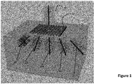
- the Figure 1 shows schematically what happens when a plane electromagnetic wave referenced 101 hits a diffractive grating structure referenced 102 that comprises a set of lines or slabs or slits.
- the diffractive grating structure 102 is positioned on a propagation layer. Due to the presence of the lines, the incident electromagnetic wave 101 is divided into diffraction modes, which are angular spaced beams of local maximum intensity.
- the five diffracted modes number are represented (respectively the diffraction mode -2 (referenced as 107 in Figure 1 ), the diffraction mode -1 (referenced as 106 in the Figure 1 ), the diffraction mode 0 (referenced as 103 in the Figure 1 ), the diffraction mode 1 (referenced as 104 in the Figure 1 ), and the diffraction mode 2 (referenced as 105 in the Figure 1 ).
- diffraction mode -2 referenced as 107 in Figure 1
- the diffraction mode -1 referenced as 106 in the Figure 1
- the diffraction mode 0 referenced as 103 in the Figure 1
- the diffraction mode 1 referenced as 104 in the Figure 1
- the diffraction mode 2 referenced as 105 in the Figure 1 .
- More details concerning a diffraction grating structure can be obtained in the section 5.6 of the document entitled "Diffraction, Fourier Optics and Imaging " by Okan K. Er
- the order zero 103 has in general the more power and is the natural mode into which the regular refraction or reflection would occur.
- a diffraction grating structure generates a lot of diffraction orders. In numerous applications it is wishful to suppress or cancel all other modes but the first one.
- n 2 ⁇ sin ⁇ 2 ⁇ n 1 ⁇ sin ⁇ 1 M . ⁇ . T
- n 1 ( ⁇ ) and n 2 ( ⁇ ) are respectively the index of refraction of the incident layer/media and the index of refraction of the diffracted layer/media (also named the propagation layer).
- the refractive index of a material is wavelength dependent. For example, the refractive index of a glass increases as the wavelength of incident light gets shorter (see figure 4 ).
- n 1 ( ⁇ ) 1.
- ⁇ 1 is the incident angle
- ⁇ 2 the diffracted angle
- M is the diffraction order
- ⁇ the wavelength
- T the grating frequency
- the diffraction process is very dispersive.
- the refraction is different for different wavelength as the index is frequency dependent, but the diffraction varies linearly with the wavelength ( M ⁇ T ) which is quite a big variation. It is therefore necessary to find a mean to minimize chromatic aberrations.
- One way, but not the preferred one, is to design the wave guide as part of the light source device and balance that chromatic aberration with different set of glasses in the projection lens.
- the field of view is defined as the difference between the limit incident angles for the incoming electromagnetic waves that can be propagated into the wave guide. Therefore, in view of the Figure 2 , it appears that the field of view is defined by the value ⁇ 1 + - ⁇ 1 - , where the values ⁇ 1 - and ⁇ 1 + corresponds respectively to the limit incident angles for the incoming electromagnetic waves that can propagate into the wave guide. Indeed, if an incident electromagnetic wave hits a diffraction structure with a given angle that is not comprised in the interval [ ⁇ 1 + ; ⁇ 1 - ], then no propagation of the incident electromagnetic wave occurs.
- an incident electromagnetic wave hits a diffraction structure with a given angle that is comprised in the interval [ ⁇ 1 + ; ⁇ 1 - ].
- a propagation of the incident electromagnetic wave occurs.
- the incident electromagnetic wave referenced 202 that hits the diffraction grating structure with a limit angle ⁇ 1 + is propagated in the propagation layer according to total internal reflection according to the path referenced 203.
- the incident electromagnetic wave referenced 201 that hits the diffraction grating structure with a limit angle ⁇ 1 - is propagated in the propagation layer according to total internal reflection according to the path referenced 204.
- an incident electromagnetic wave in order to be propagate into the propagation layer, an incident electromagnetic wave must have an incident angle ⁇ 1 that must fulfill the following conditions: sin ⁇ 1 1 ⁇ ⁇ T ⁇ ⁇ 1 ⁇ sin ⁇ 1 n 2 ⁇ ⁇ ⁇ T .
- ⁇ ⁇ 1 sin -1 ( n 2 ( ⁇ ) - ⁇ T ) + sin -1 (1 - ⁇ T ) after introducing the expression for T as defined in equation (6).
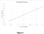
- Figure 3 shows a graph for some examples of ranges of n 2 .
- n 2 1.684 for the d spectral line.
- optical glasses with very interesting characteristics for such an application, whose cost is comparable to BK7, for instance the glass LASF35 from Schott's catalog has an index of (2.046/F, 2.023/d, 2.012C) and gets a field of view a little bit above 60 degrees diagonal, which shows the very strong dependence of the FoV on the material of the waveguide.
- the total field of view does not depend on the wavelength (except for the refractive index, but such link has a small impact in term of variations). This is an interesting observation because this means that, although the diffraction orders angular spectrum strongly varies with the wavelength, the field of view for one order (here the first order) only depends on the index of refraction, which is the normal dependence in lens design tasks and could be balanced out by a join design with the main lens of the light engine.
- a solar cell can be made of an anode positioned on a glass substrate, a cathode, and between the anode and the cathode, an organic semiconductor.
- the anode is usually a transparent anode (for example the anode is made of indium tin oxide (ITO)).
- ITO indium tin oxide
- a solar cell can be made of an anode positioned on a glass substrate, a cathode, and between the anode and the cathode, a bulk heteojunction.
- the anode is usually a transparent anode (for example the anode is made of indium tin oxide (ITO)).
- equation (7) leads to a maximum field of view of 180 for n 2 ⁇ 3.
- the solar cell comprises a diffraction grating structure that has a frequency of lines that is defined according to a wavelength comprised in the range 495-570 nm (i.e. corresponding to the green).
- a diffraction grating structure designed for privileging the "green" electromagnetic waves as the radiate energy from incident light received from the sun on Earth is dominated by wavelengths comprised in the range 495-570 nm.
- an OLED cell comprises an anode positioned on a glass substrate, a cathode, and between the anode and the cathode, active layers that comprise an electron transport layer (ETL) and a hole transport layer (HTL).
- the anode is made of a transparent material in order to allow light to leave active layers.
- the anode can be made of an indium tin oxide (ITO).
- ITO indium tin oxide
- a light emitting material LEM can also be positioned between the HTL and the ETL. It should be noted that the color emitted by an OLED is determined or linked by the nature of the LEM.
- the proposed diffraction grating is positioned to receive the lights or electromagnetic waves and then to favor or privilege the first diffraction order waves resulting from the diffraction process linked to the structure of the diffraction grating according to one embodiment of the disclosure.
- the field of view is of about 41 degrees so the plane waves with incidence angles of -20,-10,0,10 and 20 degrees can be used.
- the field of view is of about 60 degrees so the plane waves with incidence angles of -30,-20, -10,0,10, 20 and 30 degrees can be used.
Landscapes
- Physics & Mathematics (AREA)
- Optics & Photonics (AREA)
- General Physics & Mathematics (AREA)
- Engineering & Computer Science (AREA)
- Microelectronics & Electronic Packaging (AREA)
- Diffracting Gratings Or Hologram Optical Elements (AREA)
Abstract
In one embodiment of the disclosure, it is proposed diffraction grating structure comprising several grating lines. The diffraction grating structure is associated with a propagation layer, and the diffraction grating structure is made of a material that has a refractive index being equal to(). The diffraction grating structure is remarkable in that it comprises 1/T grating lines per µm, with= (() + 1)/, whereis a wavelength defined from an incident electromagnetic wave.
Description
- The disclosure relates to a technique for enhancing the field of view associated with a diffraction grating structure.
- This section is intended to introduce the reader to various aspects of art, which may be related to various aspects of the present invention that are described and/or claimed below. This discussion is believed to be helpful in providing the reader with background information to facilitate a better understanding of the various aspects of the present invention. Accordingly, it should be understood that these statements are to be read in this light, and not as admissions of prior art. More precisely, in the following, the context of augmented reality glasses will be discussed. However, the present technique can also be applied to a solar cell for harvesting energy or also to an OLED (which stands for Organic Light-Emitting Diode) cell (that is part of an OLED display device).
- Augmented reality glasses (AR) or see through glasses or near-eyes display glasses enable a user to mix added information or virtual data with the real world.
- Therefore, a user that wears such kind of device enjoys new experiment, and it provides a way to enhance the real world that surrounds us. In order to achieve such effect, one solution consists in having a system with an augmented reality glasses (AR) that comprises a picture generation unit (that can generate image angular content or virtual image that is an afocal image) associated with a given field of view, a light source unit for generating a light representation of the picture, an input grating and an optical waveguide, an horizontal eye box magnification, a vertical eye box magnification, and an output grating for delivering the light representation of the picture to the eye box of the user.
- The function of the input grating is to receive the biggest possible field of view (FoV) and to deviate the light coming from the light source within the optical waveguide in such way the light is guided inside by total internal reflection (TIR) without the degradation of the virtual image.
- Examples of augmented reality glasses (AR) are depicted in documents
WO2017180403, US2012127577 ,US9019615 US 20090128911 . - However, common input grating design suffers from limitation on the size of possible field of views. Even if techniques have been developed for extending the size of possible field of views (see for example document
WO 2017180403 ), the obtained results are still not satisfying for the users. The proposed technique tries to overcome these limitations. - References in the specification to "one embodiment", "an embodiment", "an example embodiment", indicate that the embodiment described may include a particular feature, structure, or characteristic, but every embodiment may not necessarily include the particular feature, structure, or characteristic. Moreover, such phrases are not necessarily referring to the same embodiment. Further, when a particular feature, structure, or characteristic is described in connection with an embodiment, it is submitted that it is within the knowledge of one skilled in the art to affect such feature, structure, or characteristic in connection with other embodiments whether or not explicitly described.
- In one embodiment of the disclosure, it is proposed a diffraction grating structure comprising several grating lines. The diffraction grating structure is associated with a propagation layer, and the diffraction grating structure is made of a material that has a refractive index which is equal to n 2(λ). The diffraction grating structure is remarkable in that it comprises 1/T grating lines per µm, with T = (n 2(λ) + 1)/λ, where λ is a wavelength defined from an incident electromagnetic wave.
- Indeed, λ is defined as a function of an incident electromagnetic wave. In one embodiment of the disclosure, when the incident electromagnetic wave is polychromatic, the value of λ used for defining T is obtained from the different wavelengths of an incident electromagnetic wave. In another embodiment, when the incident electromagnetic wave is monochromatic, the value of λ used for defining T is obtained directly from the wavelength of the incident electromagnetic wave.
- In a preferred embodiment, the refractive index n 2(λ) is comprised between 1.54 and 1.51 when a wavelength of an incident electromagnetic wave is belonging to a range of 400 nm-800 nm.
- In a preferred embodiment, the wavelength of an incident electromagnetic wave is around 486 nm. Indeed, the wavelength of an incident electromagnetic wave is associated with the blue color.
- In a preferred embodiment, the wavelength of an incident electromagnetic wave is around 588 nm. Indeed, the wavelength of an incident electromagnetic wave is associated with the green color.
- In a preferred embodiment, the wavelength of an incident electromagnetic wave is around 656 nm. Indeed, the wavelength of an incident electromagnetic wave is associated with the red color.
- In a preferred embodiment, the propagation layer and the diffraction grating structure have a same refractive index.
- In a preferred embodiment, the propagation layer and the diffraction grating structure have different refractive indexes.
- In a preferred embodiment, it is proposed an optical device comprising a light emitting source that can emit electromagnetic waves that correspond to at least one of the three primary colors among the red, blue and green colors, and an optical waveguide for guiding light emitted by said light emitting source. The optical device further comprises a diffraction grating structure intended to received light, from a specific color, as previously mentioned.
- In a preferred embodiment, the optical device further comprises at least another diffraction grating structure comprising several grating lines. Such another diffraction grating is positioned on the diffraction grating, and the at least another diffraction grating is made of a material having a refractive index being equal to n 3(λ). Such another diffraction grating is remarkable in that it comprises 1/T grating lines per µm, with T = (n 3(λ) + 1)/λ.
- In a preferred embodiment, each incident electromagnetic wave is normal compared to diffraction grating structures comprised in said optical device.
- In a preferred embodiment, the grating lines of the diffraction grating structure define a rectangle with a length of 1 to 10 mm, and a width of 1 a 10 mm.
- In a variant, it is proposed an OLED cell, comprising an anode positioned on a glass substrate, a cathode, and between the anode and the cathode respectively an electron transport layer, a light emitting material, and a hole transport layer, the light emitting material being associated with a light color. The OLED cell comprises a diffraction grating structure positioned on said glass substrate and the wavelength of the incident electromagnetic wave corresponds to the one associated with said light color.
- In a preferred embodiment, the grating lines of the diffraction grating structure define a surface that covers 50 % of the glass substrate of the OLED cell.
- In a variant, it is proposed a solar cell comprising a diffraction grating structure as mentioned previously. In addition, λ is chosen as being equal to 588 nm and the incident electromagnetic wave corresponds to light coming from the sun.
- In a preferred embodiment of the disclosure, the grating lines covers all the surface of the solar cell.
- The above and other aspects of the invention will become more apparent by the following detailed description of exemplary embodiments thereof with reference to the attached drawings in which:
-
Figure 1 presents an example of a diffraction process performed by a diffraction grating structure as known in the prior art; -
Figure 2 presents an example of a diffraction process performed by a diffraction grating structure according to one embodiment of the disclosure; -
Figure 3 presents the correlation or relationship that links the index of refraction of a propagation layer and the field of view when using a diffraction grating according to one embodiment of the disclosure; -
Figure 4 presents the relationship between the index of refraction of a glass material and an incident electromagnetic wave; -
Figure 5 presents the relationship between the index of refraction of silicon material and an incident electromagnetic wave. - According to one embodiment of the disclosure, it is proposed a diffractive grating structure that comprises a linear array of sub-wavelength structures to diffract the light that comes from either a light source device (as for example the light sources in documents
WO 2017180403 ,US2012127577 ,US9019615 US20090128911 ) or from another source of light (such as the sun for example). It should be noted that the light source device can emit either monochromatic light or polychromatic light according to the intended use or goal. - In order to describe the present disclosure, it is proposed to remind the reader with the diffractive process that one can observe in presence with a conventional diffractive grating structure (as the one mentioned in the previously mentioned documents
WO 2017180403 ,US2012127577 ,US9019615 US 20090128911 ). TheFigure 1 shows schematically what happens when a plane electromagnetic wave referenced 101 hits a diffractive grating structure referenced 102 that comprises a set of lines or slabs or slits. Thediffractive grating structure 102 is positioned on a propagation layer. Due to the presence of the lines, the incidentelectromagnetic wave 101 is divided into diffraction modes, which are angular spaced beams of local maximum intensity. In thefigure 1 , the five diffracted modes number are represented (respectively the diffraction mode -2 (referenced as 107 inFigure 1 ), the diffraction mode -1 (referenced as 106 in theFigure 1 ), the diffraction mode 0 (referenced as 103 in theFigure 1 ), the diffraction mode 1 (referenced as 104 in theFigure 1 ), and the diffraction mode 2 (referenced as 105 in theFigure 1 ). Obviously, other higher or smaller orders exist, but they are not represented in theFigure 1 in order to ease the understanding of the content ofFigure 1 . More details concerning a diffraction grating structure can be obtained in the section 5.6 of the document entitled "Diffraction, Fourier Optics and Imaging" by Okan K. Ersoy, published by John Wiley & Sons. - The order zero 103 has in general the more power and is the natural mode into which the regular refraction or reflection would occur. In general, a diffraction grating structure generates a lot of diffraction orders. In numerous applications it is wishful to suppress or cancel all other modes but the first one.
- Hence, there is a need to provide a diffraction grating structure that can heavily privilege the first diffraction order and reduce (or suppress) as much as possible the other diffraction orders.
- We focus hereafter the coupling into a wave guide of the first diffraction order. In fact, all diffraction orders are linked to the incoming electromagnetic wave by the following equation (referenced as equation (1)):

figure 4 ). The same remark can be done for silicon material (seefigure 5 ). In most case n 1(λ) = 1. The following notations are also used: θ 1 is the incident angle, θ 2 the diffracted angle, M is the diffraction order, λ the wavelength and T the grating frequency, which is expressed in lines per µm if the wavelength is also expressed in µm. - Therefore, for the zero-diffraction order (i.e. M = 0), the equation (1) is reduced to the well-known Snell-Descartes's law of refraction.
- One can notice that the diffraction process is very dispersive. The refraction is different for different wavelength as the index is frequency dependent, but the diffraction varies linearly with the wavelength (MλT) which is quite a big variation. It is therefore necessary to find a mean to minimize chromatic aberrations. One way, but not the preferred one, is to design the wave guide as part of the light source device and balance that chromatic aberration with different set of glasses in the projection lens.
- For that purpose, the wavelength used to correct this aberration are the Fraunhofer F, d, C spectral lines which are used to optimize the glass constringences in the glass substitution method to minimize lateral and longitudinal chroma: (F, d, C) = (0,486; 0.588; 0.656) µm.
- More details concerning the Fraunhofer spectral lines are given in the document entitled "Spectroscopy for Amateur Astronomers: Recording, Processing, Analysis and Interpretation" by Marc F. M. Tristen and Richard Walker.
- All notations being set, we can calculate now the Field of View (FoV) of a waveguide. Indeed, the field of view is defined as the difference between the limit incident angles for the incoming electromagnetic waves that can be propagated into the wave guide. Therefore, in view of the
Figure 2 , it appears that the field of view is defined by the value θ 1 + - θ 1 -, where the values θ 1 - and θ 1 + corresponds respectively to the limit incident angles for the incoming electromagnetic waves that can propagate into the wave guide. Indeed, if an incident electromagnetic wave hits a diffraction structure with a given angle that is not comprised in the interval [θ 1 +; θ 1 -], then no propagation of the incident electromagnetic wave occurs. However, if an incident electromagnetic wave hits a diffraction structure with a given angle that is comprised in the interval [θ 1 +; θ 1 -], then a propagation of the incident electromagnetic wave occurs. For example, in thefigure 2 , the incident electromagnetic wave referenced 202 that hits the diffraction grating structure with a limit angle θ 1 +, is propagated in the propagation layer according to total internal reflection according to the path referenced 203. In the same way, the incident electromagnetic wave referenced 201 that hits the diffraction grating structure with a limit angle θ 1 -, is propagated in the propagation layer according to total internal reflection according to the path referenced 204. - The critical angle θ 2c (being equal to either θ 1 + or θ 1 -, is defined by the following equation (referenced as equation 2):

equation 1 with this one leads then to the lowest possible in coupling angle that still traps the first diffraction order (equation referenced as equation (3)):

- Which is equivalent to θ 1 + ≤ sin -1(n 2(λ) - λT).
- Hence, finally, in order to be propagate into the propagation layer, an incident electromagnetic wave must have an incident angle θ 1 that must fulfill the following conditions:

equations 
- In order to have some values in mind, the grating frequencies for a dispersion less waveguide of index 1.5 are: (B(0:486); G(0:588); R(0:656)) = (2:57; 2:13; 1:91) lines=µm.
- The fact that they are so different suggests strongly to use a specific grating for each of the primaries. It is going to be very difficult, due to the strong dispersion by diffraction to handle the whole visible range with a unique waveguide.
- The field of view is equal to Δθ 1 = sin -1(n 2(λ) - λT) + sin -1(1 - λT) after introducing the expression for T as defined in equation (6).
- Hence, we have a field of view which is equal to

-
Figure 3 shows a graph for some examples of ranges of n 2. For n 2 = 1.5, the total field of view is rather limited to Δθ 1 = 28.96 degrees. In order to get to a field of view of 40 degrees, like the Wave Optics guide, it is preferable to use a material with n 2 = 1.684 for the d spectral line. - In fact, there are optical glasses with very interesting characteristics for such an application, whose cost is comparable to BK7, for instance the glass LASF35 from Schott's catalog has an index of (2.046/F, 2.023/d, 2.012C) and gets a field of view a little bit above 60 degrees diagonal, which shows the very strong dependence of the FoV on the material of the waveguide. Of course, for the LASF35 glass, the grating frequencies need to be matched to the index and we would need to use T = (3.11(F), 2.57(d), 2.30 (C)) lines per µm.
- It should also be noted that a field of view having a value of 60 degrees should be considered as the limit for flat wave guides because there are no other materials of refractive index above 2.0 for the moment.
- In addition, it should be noted that the total field of view, as defined in equation (7) does not depend on the wavelength (except for the refractive index, but such link has a small impact in term of variations). This is an interesting observation because this means that, although the diffraction orders angular spectrum strongly varies with the wavelength, the field of view for one order (here the first order) only depends on the index of refraction, which is the normal dependence in lens design tasks and could be balanced out by a join design with the main lens of the light engine.
- In another embodiment of the disclosure, it is proposed to use the previously mentioned diffraction grating in a solar cell.
- Reminders on Solar cell are provided in the section 6.15 and 6.16 of the book entitled "Principles of Solar cells, LEDs and Diodes; The role of the PN junction" by Adrian Kitai. Indeed, a solar cell can be made of an anode positioned on a glass substrate, a cathode, and between the anode and the cathode, an organic semiconductor. The anode is usually a transparent anode (for example the anode is made of indium tin oxide (ITO)). Such kind of solar cell is mentioned as a single-layer organic solar cell.
- In a variant, a solar cell can be made of an anode positioned on a glass substrate, a cathode, and between the anode and the cathode, a bulk heteojunction. The anode is usually a transparent anode (for example the anode is made of indium tin oxide (ITO)).
- The previous developments concerning the field of views can be applied to solar cells.
- It can be noted that equation (7) leads to a maximum field of view of 180 for n 2 ≥ 3. The various form of Silicon used in solar cell, mono-crystalline, polycristalline or amorphous, have all values above 3. This means that if we provide the solar cell with such a diffraction grating structure, it will couple all incoming light, whatever the angle, coming from the full half hemisphere, into a guided mode inside the silicon.
- The very practical application is that we can then reduce the solar cell thickness to some wavelength (10 µm thick for instance) and the light will still be absorbed because it will bounce into the material until total absorption, whatever the angle of incidence!
- As we can suppress or attenuate all other orders but the first one with the diffraction grating structure according to one embodiment of the disclosure, there is a potential for exploiting a low cost fabrication of highly efficient and very thin solar cells. The price and fabrication delay of solar cell seem to be very correlated to their thickness, so that adding the cost of a diffraction grating structure might be of interest.
- Once the whole surface of a solar cell gets covered by a diffraction grating structure according to one embodiment of the disclosure, it can be interesting to detail what happens to light that hits the grating from the inside. It has been observed the following when playing around with diffraction grating structures in Zemax if the diffraction grating structure is not optimized to diffract only order 1:
- Order zero : The order zero does go through the wave guide by definition. It can never be trapped inside. This is the reason it should be highly minimized by the structure producing the diffraction;
- Order 1: The first order gets totally coupled in for a 180 degrees FoV for n 2 ≥ 3.0 and for the grating frequency given by equation (6) for the particular wavelength;
- Multiple diffraction of trapped light: The light trapped into the propagation layer or wave guide can hit the diffraction structure from inside and produce multiple diffraction orders (also named secondary diffraction). All secondary diffraction orders do stay into the propagation layer or waveguide; only the order -1 will get extracted out of the propagation layer which might be considered a small loss;
- Order 2:
Order 2 gets reflected away for θ 1 ≥ 0 and coupled in for negative angles; -
Order 3 and above: Never get into the waveguide, they are reflected away by the grating; - Order -1: The same as for the order one, but the waves will propagate into the opposite direction into the waveguide;
- Order -2: Same as for
order 2, but the angles that get coupled in are θ 1 > 0; - Order -3 and less: They don't get into the waveguide.
- As a conclusion, if we have a diffraction grating which mostly generates
order 1, all light will get coupled into the propagation layer or waveguide. Once into the waveguide, it won't be extracted out even if it hits the diffraction structure from inside. This makes that technology more than suited to ultra-thin solar cells made of any form of silicon. - In a variant, the solar cell comprises a diffraction grating structure that has a frequency of lines that is defined according to a wavelength comprised in the range 495-570 nm (i.e. corresponding to the green). Indeed, as the light coming from the sun is not a monochromatic electromagnetic wave, it is more interesting to use a diffraction grating structure designed for privileging the "green" electromagnetic waves as the radiate energy from incident light received from the sun on Earth is dominated by wavelengths comprised in the range 495-570 nm.
- In another embodiment of the disclosure, it is proposed to use the previously mentioned diffraction grating within an OLED cell.
- Reminders on OLED cell are provided in the
Chapter 6 of the book entitled "Principles of Solar cells, LEDs and Diodes; The role of the PN junction" by Adrian Kitai. - To sum-up, usually, an OLED cell comprises an anode positioned on a glass substrate, a cathode, and between the anode and the cathode, active layers that comprise an electron transport layer (ETL) and a hole transport layer (HTL). Generally, the anode is made of a transparent material in order to allow light to leave active layers. For example, the anode can be made of an indium tin oxide (ITO). In a variant, a light emitting material (LEM) can also be positioned between the HTL and the ETL. It should be noted that the color emitted by an OLED is determined or linked by the nature of the LEM. Hence, it is possible to choose specific material of the LEM in order to obtain an OLED cell that only delivers monochromatic electromagnetic wave (i.e. monochromatic light). Therefore, the proposed diffraction grating is positioned to receive the lights or electromagnetic waves and then to favor or privilege the first diffraction order waves resulting from the diffraction process linked to the structure of the diffraction grating according to one embodiment of the disclosure.
- Usually, in OLED cells, there is only a small portion of light that gets out of the cell. Because the light has been generated into a much denser media than air, the biggest amount is trapped into the structure by total internal reflection phenomenon. In the previous section, it has been explained that trapped light can get totally extracted if it hits a diffraction grating which is optimized for the order -1.
- In fact, it seems that on both sides of the barrier between the air and dense media, if diffracted
order 1 gets trapped into the structure, the diffraction order -1 gets extracted. Hence,order 1 and -1 do play complementary roles on both sides of the grating. - In order to achieve an efficient extraction, it is used a so called thick grating, whose thickness can have 10 µm. This kind of extraction device is only interesting if the lateral cell structures are pixels of much larger size.
- Hence, if thin diffraction gratings are used, only the order -1 is extracted at each bouncing on the grating.
- Still, by recurrent round trips of the light into the OLED cell, there will be significantly more light extracted by the grating, even if it is not optimized for order -1.
- In one embodiment of the disclosure, it is proposed to use a diffraction grating structure, with n 1 = 1, n 2 = 1.7 that comprises different parts comprising respectively grating lines having the following frequencies: 2.78, 2.30 and 2.06 lines per µm, and these different parts are intended to receive respectively only one kind of electromagnetic waves having the following wavelengths: 0.486, 0.588 and 0.656 µm. In such embodiment, the field of view is of about 41 degrees so the plane waves with incidence angles of -20,-10,0,10 and 20 degrees can be used. We can assume as a starting point that the material is non-dispersive.
- In another embodiment of the disclosure, it is proposed to use diffraction grating structure, with n 1 = 1, n 2 = 2.0 that comprises different parts comprising respectively grating lines having the following frequencies: 3.09, 2.55 and 2.29 lines per µm, and these different parts are intended to receive respectively only one kind of electromagnetic waves having the following wavelengths: 0.486, 0.588 and 0.656 µm. In such embodiment, the field of view is of about 60 degrees so the plane waves with incidence angles of -30,-20, -10,0,10, 20 and 30 degrees can be used. We can assume as a starting point that the material is non-dispersive.
- In another embodiment of the disclosure, it is proposed to superpose the diffractive grating structures.
Claims (15)
- A diffraction grating structure comprising several grating lines, said diffraction grating structure being associated with a propagation layer, said diffraction grating structure being made of a material that has a refractive index being equal to n 2(λ), the diffraction grating structure being characterized in that it comprises 1/T grating lines per µm, with T = (n 2(λ) + 1)/λ, where λ is a wavelength defined from an incident electromagnetic wave.
- The diffraction grating according to claim 1, wherein the refractive index n 2(λ) is comprised between 1.54 and 1.51 when a wavelength of an incident electromagnetic wave is belonging to a range of 400 nm-800 nm.
- The diffraction grating according to claim 1, wherein said material is silicon.
- The diffraction grating according to any claims 1 to 3, wherein a wavelength of the incident electromagnetic wave is around 486 nm.
- The diffraction grating according to any claims 1 to 3, wherein a wavelength of the incident electromagnetic wave is around 588 nm.
- The diffraction grating according to any claims 1 to 3, wherein a wavelength of the incident electromagnetic wave is around 656 nm.
- The diffraction grating according to any claims 1 to 6, wherein said propagation layer and said diffraction grating structure have a same refractive index.
- The diffraction grating according to any claims 1 to 6, wherein said propagation layer and said diffraction grating structure have different refractive indexes.
- An optical device comprising a light emitting source that can emit electromagnetic waves that correspond to at least one of the three primary colors among the red, blue and green colors, and an optical waveguide for guiding light emitted by said light emitting source, wherein said optical device further comprises a diffraction grating structure intended to received light, from a specific color, according to claim 1.
- The optical device according to claim 9, wherein it further comprises at least another diffraction grating structure comprising several grating lines, said another diffraction grating being positioned on said diffraction grating, said at least another diffraction grating being made of a material having a refractive index being equal to n 3(λ), said another diffraction grating being characterized in that it comprises 1/T grating lines per µm, with T = (n 3(λ) + 1)/λ.
- The optical device according to any claims 9 to 10, wherein each incident electromagnetic wave is normal compared to diffraction grating structures comprised in said optical device.
- The optical device according to any claims 9 to 11, wherein the grating lines of said diffraction grating structure define a rectangle with a length of 1 to 10 mm, and a width of 1 à 10 mm.
- An OLED cell, comprising an anode positioned on a glass substrate, a cathode, and between the anode and the cathode respectively an electron transport layer, a light emitting material, and a hole transport layer, the light emitting material being associated with a light color, wherein said OLED cell comprises a diffraction grating structure positioned on said glass substrate according to claim 1, wherein the wavelength of the incident electromagnetic wave corresponds to the one associated with said light color.
- The OLED cell according to claim 13, wherein the grating lines of said diffraction grating structure define a surface that covers 50 % of said glass substrate of said OLED cell.
- A solar cell comprising a diffraction grating structure according to claim 1, wherein λ is chosen as being equal to 588 nm and the incident electromagnetic wave being light coming from the sun.
Priority Applications (6)
| Application Number | Priority Date | Filing Date | Title |
|---|---|---|---|
| EP17306763.8A EP3499278A1 (en) | 2017-12-13 | 2017-12-13 | A diffraction grating structure comprising several grating lines |
| US16/954,157 US20210088705A1 (en) | 2017-12-13 | 2018-12-11 | A diffraction grating structure comprising several grating lines |
| PCT/EP2018/084269 WO2019115488A1 (en) | 2017-12-13 | 2018-12-11 | A diffraction grating structure comprising several grating lines |
| CN201880085971.7A CN111788501B (en) | 2017-12-13 | 2018-12-11 | Diffraction grating structure comprising a plurality of grating lines |
| EP18814613.8A EP3724703A1 (en) | 2017-12-13 | 2018-12-11 | A diffraction grating structure comprising several grating lines |
| US18/525,016 US20240103208A1 (en) | 2017-12-13 | 2023-11-30 | Diffraction grating structure comprising several grating lines |
Applications Claiming Priority (1)
| Application Number | Priority Date | Filing Date | Title |
|---|---|---|---|
| EP17306763.8A EP3499278A1 (en) | 2017-12-13 | 2017-12-13 | A diffraction grating structure comprising several grating lines |
Publications (1)
| Publication Number | Publication Date |
|---|---|
| EP3499278A1 true EP3499278A1 (en) | 2019-06-19 |
Family
ID=60888310
Family Applications (2)
| Application Number | Title | Priority Date | Filing Date |
|---|---|---|---|
| EP17306763.8A Withdrawn EP3499278A1 (en) | 2017-12-13 | 2017-12-13 | A diffraction grating structure comprising several grating lines |
| EP18814613.8A Pending EP3724703A1 (en) | 2017-12-13 | 2018-12-11 | A diffraction grating structure comprising several grating lines |
Family Applications After (1)
| Application Number | Title | Priority Date | Filing Date |
|---|---|---|---|
| EP18814613.8A Pending EP3724703A1 (en) | 2017-12-13 | 2018-12-11 | A diffraction grating structure comprising several grating lines |
Country Status (4)
| Country | Link |
|---|---|
| US (2) | US20210088705A1 (en) |
| EP (2) | EP3499278A1 (en) |
| CN (1) | CN111788501B (en) |
| WO (1) | WO2019115488A1 (en) |
Cited By (26)
| Publication number | Priority date | Publication date | Assignee | Title |
|---|---|---|---|---|
| US11442222B2 (en) | 2019-08-29 | 2022-09-13 | Digilens Inc. | Evacuated gratings and methods of manufacturing |
| US11543594B2 (en) | 2019-02-15 | 2023-01-03 | Digilens Inc. | Methods and apparatuses for providing a holographic waveguide display using integrated gratings |
| US11573356B2 (en) | 2018-03-13 | 2023-02-07 | Interdigital Ce Patent Holdings | Diffraction grating comprising double-materials structures |
| US11604363B2 (en) | 2018-03-13 | 2023-03-14 | Interdigital Ce Patent Holdings | Image sensor comprising a color splitter with two different refractive indexes |
| US11709373B2 (en) | 2014-08-08 | 2023-07-25 | Digilens Inc. | Waveguide laser illuminator incorporating a despeckler |
| US11726329B2 (en) | 2015-01-12 | 2023-08-15 | Digilens Inc. | Environmentally isolated waveguide display |
| US11726323B2 (en) | 2014-09-19 | 2023-08-15 | Digilens Inc. | Method and apparatus for generating input images for holographic waveguide displays |
| US11754842B2 (en) | 2015-10-05 | 2023-09-12 | Digilens Inc. | Apparatus for providing waveguide displays with two-dimensional pupil expansion |
| US11972508B2 (en) | 2018-07-02 | 2024-04-30 | Interdigital Ce Patent Holdings, Sas | Image sensor comprising a color splitter with two different refractive indexes, and different height |
| US12140764B2 (en) | 2019-02-15 | 2024-11-12 | Digilens Inc. | Wide angle waveguide display |
| US12158612B2 (en) | 2021-03-05 | 2024-12-03 | Digilens Inc. | Evacuated periodic structures and methods of manufacturing |
| US12174512B2 (en) | 2018-12-18 | 2024-12-24 | Interdigital Ce Patent Holdings | Device for forming an outgoing electromagnetic wave from an incident electromagnetic wave |
| US12210155B2 (en) | 2018-06-29 | 2025-01-28 | Interdigital Ce Patent Holdings | Optical device comprising a multi-layers waveguides |
| US12210153B2 (en) | 2019-01-14 | 2025-01-28 | Digilens Inc. | Holographic waveguide display with light control layer |
| US12214493B2 (en) | 2018-12-18 | 2025-02-04 | Interdigital Ce Patent Holdings, Sas | Optical manipulation apparatus |
| US12228756B2 (en) | 2018-12-21 | 2025-02-18 | Interdigital Ce Patent Holdings, Sas | Optical device |
| US12248150B2 (en) | 2017-01-05 | 2025-03-11 | Digilens Inc. | Wearable heads up displays |
| US12271035B2 (en) | 2019-06-07 | 2025-04-08 | Digilens Inc. | Waveguides incorporating transmissive and reflective gratings and related methods of manufacturing |
| US12298513B2 (en) | 2016-12-02 | 2025-05-13 | Digilens Inc. | Waveguide device with uniform output illumination |
| US12306585B2 (en) | 2018-01-08 | 2025-05-20 | Digilens Inc. | Methods for fabricating optical waveguides |
| US12366823B2 (en) | 2018-01-08 | 2025-07-22 | Digilens Inc. | Systems and methods for high-throughput recording of holographic gratings in waveguide cells |
| US12379547B2 (en) | 2015-02-12 | 2025-08-05 | Digilens Inc. | Waveguide grating device |
| US12397477B2 (en) | 2019-02-05 | 2025-08-26 | Digilens Inc. | Methods for compensating for optical surface nonuniformity |
| US12405507B2 (en) | 2012-11-16 | 2025-09-02 | Digilens Inc. | Transparent waveguide display with grating lamina that both couple and extract modulated light |
| US12596218B2 (en) | 2012-04-25 | 2026-04-07 | Digilens Inc. | Holographic wide angle display |
| US12613439B2 (en) | 2018-01-08 | 2026-04-28 | Digilens Inc. | Systems and methods for manufacturing waveguide cells |
Citations (6)
| Publication number | Priority date | Publication date | Assignee | Title |
|---|---|---|---|---|
| US20080043334A1 (en) * | 2006-08-18 | 2008-02-21 | Mirage Innovations Ltd. | Diffractive optical relay and method for manufacturing the same |
| US20090128911A1 (en) | 2005-09-14 | 2009-05-21 | Moti Itzkovitch | Diffraction Grating With a Spatially Varying Duty-Cycle |
| US20120127577A1 (en) | 2009-07-31 | 2012-05-24 | Horiba Jobin Yvon Sas | Planar optical system for wide field-of-view polychromatic imaging |
| US9019615B2 (en) | 2012-06-12 | 2015-04-28 | Microsoft Technology Licensing, Llc | Wide field-of-view virtual image projector |
| US9442227B2 (en) * | 2011-07-05 | 2016-09-13 | Council Of Scientific & Industrial Research | Planar solar concentrators using subwavelength gratings |
| WO2017180403A1 (en) | 2016-04-13 | 2017-10-19 | Microsoft Technology Licensing, Llc | Waveguides with extended field of view |
Family Cites Families (6)
| Publication number | Priority date | Publication date | Assignee | Title |
|---|---|---|---|---|
| CN101833138B (en) * | 2010-04-30 | 2012-01-25 | 华中科技大学 | Method for manufacturing polarization-independent grating coupler |
| CN102902002B (en) * | 2012-09-25 | 2014-06-25 | 浙江大学 | Reflection type volume holographic Bragg grating ultraviolet exposure method |
| KR20150136504A (en) * | 2013-03-28 | 2015-12-07 | 미쯔비시 레이온 가부시끼가이샤 | Optical film, optical film manufacturing method and surface light-emitting body |
| US9939628B2 (en) * | 2014-03-20 | 2018-04-10 | CSEM Centre Suisse d'Electronique et de Microtechnique SA—Recherche et Développement | Imaging system |
| JP6597197B2 (en) * | 2015-11-05 | 2019-10-30 | セイコーエプソン株式会社 | Beam diameter expanding element and display device |
| JP6677036B2 (en) * | 2016-03-23 | 2020-04-08 | セイコーエプソン株式会社 | Image display device and optical element |
-
2017
- 2017-12-13 EP EP17306763.8A patent/EP3499278A1/en not_active Withdrawn
-
2018
- 2018-12-11 US US16/954,157 patent/US20210088705A1/en not_active Abandoned
- 2018-12-11 EP EP18814613.8A patent/EP3724703A1/en active Pending
- 2018-12-11 CN CN201880085971.7A patent/CN111788501B/en active Active
- 2018-12-11 WO PCT/EP2018/084269 patent/WO2019115488A1/en not_active Ceased
-
2023
- 2023-11-30 US US18/525,016 patent/US20240103208A1/en not_active Abandoned
Patent Citations (6)
| Publication number | Priority date | Publication date | Assignee | Title |
|---|---|---|---|---|
| US20090128911A1 (en) | 2005-09-14 | 2009-05-21 | Moti Itzkovitch | Diffraction Grating With a Spatially Varying Duty-Cycle |
| US20080043334A1 (en) * | 2006-08-18 | 2008-02-21 | Mirage Innovations Ltd. | Diffractive optical relay and method for manufacturing the same |
| US20120127577A1 (en) | 2009-07-31 | 2012-05-24 | Horiba Jobin Yvon Sas | Planar optical system for wide field-of-view polychromatic imaging |
| US9442227B2 (en) * | 2011-07-05 | 2016-09-13 | Council Of Scientific & Industrial Research | Planar solar concentrators using subwavelength gratings |
| US9019615B2 (en) | 2012-06-12 | 2015-04-28 | Microsoft Technology Licensing, Llc | Wide field-of-view virtual image projector |
| WO2017180403A1 (en) | 2016-04-13 | 2017-10-19 | Microsoft Technology Licensing, Llc | Waveguides with extended field of view |
Non-Patent Citations (2)
| Title |
|---|
| MARC F. M. TRISTEN; RICHARD WALKER, SPECTROSCOPY FOR AMATEUR ASTRONOMERS: RECORDING, PROCESSING, ANALYSIS AND INTERPRETATION |
| OKAN K. ERSOY: "Diffraction, Fourier Optics and Imaging", JOHN WILEY & SONS |
Cited By (31)
| Publication number | Priority date | Publication date | Assignee | Title |
|---|---|---|---|---|
| US12596218B2 (en) | 2012-04-25 | 2026-04-07 | Digilens Inc. | Holographic wide angle display |
| US12405507B2 (en) | 2012-11-16 | 2025-09-02 | Digilens Inc. | Transparent waveguide display with grating lamina that both couple and extract modulated light |
| US11709373B2 (en) | 2014-08-08 | 2023-07-25 | Digilens Inc. | Waveguide laser illuminator incorporating a despeckler |
| US11726323B2 (en) | 2014-09-19 | 2023-08-15 | Digilens Inc. | Method and apparatus for generating input images for holographic waveguide displays |
| US11726329B2 (en) | 2015-01-12 | 2023-08-15 | Digilens Inc. | Environmentally isolated waveguide display |
| US11740472B2 (en) | 2015-01-12 | 2023-08-29 | Digilens Inc. | Environmentally isolated waveguide display |
| US12379547B2 (en) | 2015-02-12 | 2025-08-05 | Digilens Inc. | Waveguide grating device |
| US11754842B2 (en) | 2015-10-05 | 2023-09-12 | Digilens Inc. | Apparatus for providing waveguide displays with two-dimensional pupil expansion |
| US12405471B2 (en) | 2015-10-05 | 2025-09-02 | Digilens Inc. | Apparatus for providing waveguide displays with two-dimensional pupil expansion |
| US12298513B2 (en) | 2016-12-02 | 2025-05-13 | Digilens Inc. | Waveguide device with uniform output illumination |
| US12248150B2 (en) | 2017-01-05 | 2025-03-11 | Digilens Inc. | Wearable heads up displays |
| US12366823B2 (en) | 2018-01-08 | 2025-07-22 | Digilens Inc. | Systems and methods for high-throughput recording of holographic gratings in waveguide cells |
| US12613439B2 (en) | 2018-01-08 | 2026-04-28 | Digilens Inc. | Systems and methods for manufacturing waveguide cells |
| US12306585B2 (en) | 2018-01-08 | 2025-05-20 | Digilens Inc. | Methods for fabricating optical waveguides |
| US11573356B2 (en) | 2018-03-13 | 2023-02-07 | Interdigital Ce Patent Holdings | Diffraction grating comprising double-materials structures |
| US11604363B2 (en) | 2018-03-13 | 2023-03-14 | Interdigital Ce Patent Holdings | Image sensor comprising a color splitter with two different refractive indexes |
| US12210155B2 (en) | 2018-06-29 | 2025-01-28 | Interdigital Ce Patent Holdings | Optical device comprising a multi-layers waveguides |
| US11972508B2 (en) | 2018-07-02 | 2024-04-30 | Interdigital Ce Patent Holdings, Sas | Image sensor comprising a color splitter with two different refractive indexes, and different height |
| US12214493B2 (en) | 2018-12-18 | 2025-02-04 | Interdigital Ce Patent Holdings, Sas | Optical manipulation apparatus |
| US12174512B2 (en) | 2018-12-18 | 2024-12-24 | Interdigital Ce Patent Holdings | Device for forming an outgoing electromagnetic wave from an incident electromagnetic wave |
| US12228756B2 (en) | 2018-12-21 | 2025-02-18 | Interdigital Ce Patent Holdings, Sas | Optical device |
| US12210153B2 (en) | 2019-01-14 | 2025-01-28 | Digilens Inc. | Holographic waveguide display with light control layer |
| US12397477B2 (en) | 2019-02-05 | 2025-08-26 | Digilens Inc. | Methods for compensating for optical surface nonuniformity |
| US12140764B2 (en) | 2019-02-15 | 2024-11-12 | Digilens Inc. | Wide angle waveguide display |
| US11543594B2 (en) | 2019-02-15 | 2023-01-03 | Digilens Inc. | Methods and apparatuses for providing a holographic waveguide display using integrated gratings |
| US12271035B2 (en) | 2019-06-07 | 2025-04-08 | Digilens Inc. | Waveguides incorporating transmissive and reflective gratings and related methods of manufacturing |
| US11442222B2 (en) | 2019-08-29 | 2022-09-13 | Digilens Inc. | Evacuated gratings and methods of manufacturing |
| US11899238B2 (en) | 2019-08-29 | 2024-02-13 | Digilens Inc. | Evacuated gratings and methods of manufacturing |
| US11592614B2 (en) * | 2019-08-29 | 2023-02-28 | Digilens Inc. | Evacuated gratings and methods of manufacturing |
| JP2022546413A (en) * | 2019-08-29 | 2022-11-04 | ディジレンズ インコーポレイテッド | Vacuum grating and manufacturing method |
| US12158612B2 (en) | 2021-03-05 | 2024-12-03 | Digilens Inc. | Evacuated periodic structures and methods of manufacturing |
Also Published As
| Publication number | Publication date |
|---|---|
| US20210088705A1 (en) | 2021-03-25 |
| CN111788501B (en) | 2022-08-02 |
| US20240103208A1 (en) | 2024-03-28 |
| WO2019115488A1 (en) | 2019-06-20 |
| CN111788501A (en) | 2020-10-16 |
| EP3724703A1 (en) | 2020-10-21 |
Similar Documents
| Publication | Publication Date | Title |
|---|---|---|
| US20240103208A1 (en) | Diffraction grating structure comprising several grating lines | |
| US11906731B2 (en) | Waveguide element and waveguide stack for display applications | |
| AU2020213443B2 (en) | Highly efficient compact head-mounted display system having small input aperture | |
| US12228756B2 (en) | Optical device | |
| KR102653456B1 (en) | Waveguide displays and display devices with novel grating configurations | |
| EP2979126B1 (en) | Improvements in and relating to displays | |
| US7499216B2 (en) | Wide field-of-view binocular device | |
| US20250138234A1 (en) | Stacked waveguides having different diffraction gratings for combined field of view | |
| US8934171B2 (en) | Planar optical system for wide field-of-view polychromatic imaging | |
| US7391573B2 (en) | Substrate-guided optical devices | |
| Xu et al. | Methods of optimizing and evaluating geometrical lightguides with microstructure mirrors for augmented reality displays | |
| US20200116996A1 (en) | Display waveguide assembly with color cross-coupling | |
| GB2514658A (en) | Improvements in and relating to displays | |
| WO2020042636A1 (en) | Near-eye display device | |
| US12326562B2 (en) | Waveguide display system with wide field of view | |
| US20230134576A1 (en) | Unpolarized light grating incoupler | |
| US20230400618A1 (en) | Single mode full color waveguide combiner using asymmetric transmissive and reflective diffraction gratings | |
| KR20150071612A (en) | Ned polarization system for wavelength pass-through | |
| EP2784569A1 (en) | Improvements in and relating to displays | |
| Li et al. | Angular uniformity improvement of diffractive waveguide display based on region geometry optimization | |
| US20240264354A1 (en) | Dual diffraction grating in-coupler for reduced waveguide thickness background | |
| EP4176302B1 (en) | Full-color waveguide combiner with embedded metagrating | |
| Shramkova et al. | Design of a full color single-plate waveguide combiner with high FOV |
Legal Events
| Date | Code | Title | Description |
|---|---|---|---|
| PUAI | Public reference made under article 153(3) epc to a published international application that has entered the european phase |
Free format text: ORIGINAL CODE: 0009012 |
|
| AK | Designated contracting states |
Kind code of ref document: A1 Designated state(s): AL AT BE BG CH CY CZ DE DK EE ES FI FR GB GR HR HU IE IS IT LI LT LU LV MC MK MT NL NO PL PT RO RS SE SI SK SM TR |
|
| AX | Request for extension of the european patent |
Extension state: BA ME |
|
| STAA | Information on the status of an ep patent application or granted ep patent |
Free format text: STATUS: THE APPLICATION IS DEEMED TO BE WITHDRAWN |
|
| 18D | Application deemed to be withdrawn |
Effective date: 20191220 |