EP3493526A1 - Imaging device and imaging device control method - Google Patents
Imaging device and imaging device control method Download PDFInfo
- Publication number
- EP3493526A1 EP3493526A1 EP17836572.2A EP17836572A EP3493526A1 EP 3493526 A1 EP3493526 A1 EP 3493526A1 EP 17836572 A EP17836572 A EP 17836572A EP 3493526 A1 EP3493526 A1 EP 3493526A1
- Authority
- EP
- European Patent Office
- Prior art keywords
- addition
- mode
- unit
- pixel
- data
- Prior art date
- Legal status (The legal status is an assumption and is not a legal conclusion. Google has not performed a legal analysis and makes no representation as to the accuracy of the status listed.)
- Granted
Links
Images








Classifications
-
- H—ELECTRICITY
- H04—ELECTRIC COMMUNICATION TECHNIQUE
- H04N—PICTORIAL COMMUNICATION, e.g. TELEVISION
- H04N25/00—Circuitry of solid-state image sensors [SSIS]; Control thereof
- H04N25/40—Extracting pixel data from image sensors by controlling scanning circuits, e.g. by modifying the number of pixels sampled or to be sampled
- H04N25/42—Extracting pixel data from image sensors by controlling scanning circuits, e.g. by modifying the number of pixels sampled or to be sampled by switching between different modes of operation using different resolutions or aspect ratios, e.g. switching between interlaced and non-interlaced mode
-
- H—ELECTRICITY
- H04—ELECTRIC COMMUNICATION TECHNIQUE
- H04N—PICTORIAL COMMUNICATION, e.g. TELEVISION
- H04N23/00—Cameras or camera modules comprising electronic image sensors; Control thereof
- H04N23/60—Control of cameras or camera modules
- H04N23/667—Camera operation mode switching, e.g. between still and video, sport and normal or high- and low-resolution modes
-
- G—PHYSICS
- G06—COMPUTING OR CALCULATING; COUNTING
- G06V—IMAGE OR VIDEO RECOGNITION OR UNDERSTANDING
- G06V20/00—Scenes; Scene-specific elements
- G06V20/50—Context or environment of the image
- G06V20/52—Surveillance or monitoring of activities, e.g. for recognising suspicious objects
-
- H—ELECTRICITY
- H04—ELECTRIC COMMUNICATION TECHNIQUE
- H04N—PICTORIAL COMMUNICATION, e.g. TELEVISION
- H04N23/00—Cameras or camera modules comprising electronic image sensors; Control thereof
- H04N23/60—Control of cameras or camera modules
-
- H—ELECTRICITY
- H04—ELECTRIC COMMUNICATION TECHNIQUE
- H04N—PICTORIAL COMMUNICATION, e.g. TELEVISION
- H04N23/00—Cameras or camera modules comprising electronic image sensors; Control thereof
- H04N23/60—Control of cameras or camera modules
- H04N23/61—Control of cameras or camera modules based on recognised objects
-
- H—ELECTRICITY
- H04—ELECTRIC COMMUNICATION TECHNIQUE
- H04N—PICTORIAL COMMUNICATION, e.g. TELEVISION
- H04N25/00—Circuitry of solid-state image sensors [SSIS]; Control thereof
-
- H—ELECTRICITY
- H04—ELECTRIC COMMUNICATION TECHNIQUE
- H04N—PICTORIAL COMMUNICATION, e.g. TELEVISION
- H04N25/00—Circuitry of solid-state image sensors [SSIS]; Control thereof
- H04N25/40—Extracting pixel data from image sensors by controlling scanning circuits, e.g. by modifying the number of pixels sampled or to be sampled
- H04N25/46—Extracting pixel data from image sensors by controlling scanning circuits, e.g. by modifying the number of pixels sampled or to be sampled by combining or binning pixels
-
- H—ELECTRICITY
- H04—ELECTRIC COMMUNICATION TECHNIQUE
- H04N—PICTORIAL COMMUNICATION, e.g. TELEVISION
- H04N25/00—Circuitry of solid-state image sensors [SSIS]; Control thereof
- H04N25/50—Control of the SSIS exposure
- H04N25/53—Control of the integration time
- H04N25/533—Control of the integration time by using differing integration times for different sensor regions
- H04N25/535—Control of the integration time by using differing integration times for different sensor regions by dynamic region selection
-
- H—ELECTRICITY
- H04—ELECTRIC COMMUNICATION TECHNIQUE
- H04N—PICTORIAL COMMUNICATION, e.g. TELEVISION
- H04N25/00—Circuitry of solid-state image sensors [SSIS]; Control thereof
- H04N25/70—SSIS architectures; Circuits associated therewith
- H04N25/703—SSIS architectures incorporating pixels for producing signals other than image signals
- H04N25/707—Pixels for event detection
-
- H—ELECTRICITY
- H04—ELECTRIC COMMUNICATION TECHNIQUE
- H04N—PICTORIAL COMMUNICATION, e.g. TELEVISION
- H04N25/00—Circuitry of solid-state image sensors [SSIS]; Control thereof
- H04N25/70—SSIS architectures; Circuits associated therewith
- H04N25/71—Charge-coupled device [CCD] sensors; Charge-transfer registers specially adapted for CCD sensors
- H04N25/74—Circuitry for scanning or addressing the pixel array
-
- H—ELECTRICITY
- H04—ELECTRIC COMMUNICATION TECHNIQUE
- H04N—PICTORIAL COMMUNICATION, e.g. TELEVISION
- H04N25/00—Circuitry of solid-state image sensors [SSIS]; Control thereof
- H04N25/70—SSIS architectures; Circuits associated therewith
- H04N25/76—Addressed sensors, e.g. MOS or CMOS sensors
-
- H—ELECTRICITY
- H04—ELECTRIC COMMUNICATION TECHNIQUE
- H04N—PICTORIAL COMMUNICATION, e.g. TELEVISION
- H04N25/00—Circuitry of solid-state image sensors [SSIS]; Control thereof
- H04N25/70—SSIS architectures; Circuits associated therewith
- H04N25/76—Addressed sensors, e.g. MOS or CMOS sensors
- H04N25/779—Circuitry for scanning or addressing the pixel array
-
- H—ELECTRICITY
- H04—ELECTRIC COMMUNICATION TECHNIQUE
- H04N—PICTORIAL COMMUNICATION, e.g. TELEVISION
- H04N25/00—Circuitry of solid-state image sensors [SSIS]; Control thereof
- H04N25/70—SSIS architectures; Circuits associated therewith
- H04N25/76—Addressed sensors, e.g. MOS or CMOS sensors
- H04N25/78—Readout circuits for addressed sensors, e.g. output amplifiers or A/D converters
Definitions
- the present technology relates to an imaging apparatus and a control method for the imaging apparatus.
- the present technology relates to an imaging apparatus and a control method for the imaging apparatus that detect the presence or absence of an event such as movement of a subject.
- imaging apparatuses that detect the presence or absence of an event such as movement of a subject by an image process are widely utilized in fields such as measurement, traffic, and crime prevention.
- an imaging apparatus that captures a plurality of pieces of image data (frames) at a constant imaging interval and detects the presence or absence of an event from a difference between the integral value of the luminance of the current frame and the integral value of the luminance of the past frame (see, for example, Patent Document 1).
- This imaging apparatus is used for, for example, an application that does not record a frame in a memory until an event occurs and starts recording of a frame when an event occurs to save the memory capacity, or the like.
- Patent Document 1 Japanese Patent Application Laid-Open No. 2004-274533
- the present technology has been created in view of such a situation and it is an object of the present technology to reduce power consumption in an imaging apparatus that detects the presence or absence of an event.
- the present technology has been made in order to eliminate the above-mentioned difficulties and a first aspect thereof is an imaging apparatus and a control method therefor, the imaging apparatus including: a pixel array unit provided with a plurality of transfer transistors that transfer the charges from mutually different photoelectric conversion devices to a floating diffusion layer; a scan circuit that simultaneously controls the plurality of transfer transistors in a pixel addition mode in which pixel addition is performed, to transfer the charges, and sequentially controls the plurality of transfer transistors in a normal mode in which pixel addition is not performed, to transfer the charges; an event detection unit that detects presence or absence of a predetermined event on the basis of an addition signal which is an analog signal generated in the pixel addition mode, and generates a detection result; and a mode control unit that sets one of the pixel addition mode and the normal mode on the basis of the detection result. This brings about effectiveness that one of the pixel addition mode and the normal mode is set on the basis of the detection result for the event.
- an analog-to-digital conversion unit that performs analog-to-digital conversion on the addition signal to output as addition data may be further included. This brings about effectiveness that the addition signal is subjected to the analog-to-digital conversion.
- a predetermined number of the floating diffusion layers may be arranged in the pixel array unit, and an exposure control unit that controls an exposure amount of the pixel array unit on the basis of luminance integral data obtained by integrating the predetermined number of pieces of the addition data may be further included. This brings about effectiveness that the exposure amount is controlled on the basis of the luminance integral data.
- the event detection unit may detect presence or absence of movement of a subject as presence or absence of the predetermined event. This brings about effectiveness that one of the pixel addition mode and the normal mode is set on the basis of a detection result for the presence or absence of movement of the subject.
- the event detection unit may include: a luminance integral data holding unit that holds the luminance integral data as past integral data; and a movement detection unit that detects presence or absence of movement of the subject depending on whether or not a difference between new luminance integral data and the past integral data exceeds a predetermined threshold value. This brings about effectiveness that the presence or absence of movement of the subject is detected depending on the difference between the new luminance integral data and the past integral data.
- the event detection unit may further include: an addition data holding unit that holds the predetermined number of pieces of addition data as past addition data; and a difference acquisition unit that acquires a difference between new addition data and the past addition data corresponding to the new addition data and generates a weight according to the difference, and the luminance integral data may be a weighted addition value of the addition data and the weight corresponding to the addition data.
- the pixel array unit may generate an image signal including the analog signal in the normal mode
- the mode control unit may set the normal mode in a case where it is detected that the predetermined event has occurred, and may set the pixel addition mode in a case where a certain number of the image signals are generated. This brings about effectiveness that the pixel addition mode is set in a case where a certain number of image signals are generated.
- the pixel array unit, the scan circuit, the event detection unit, and the mode control unit may be arranged in a solid-state imaging device. This brings about effectiveness that an event is detected by the solid-state imaging device.
- the pixel array unit and the scan circuit may be arranged in a solid-state imaging device, and the event detection unit and the mode control unit may be arranged outside the solid-state imaging device. This brings about effectiveness that an event is detected outside the solid-state imaging device.
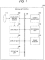
- Fig. 1 is a block diagram illustrating a configuration example of an imaging apparatus 100 according to a first embodiment of the present technology.
- This imaging apparatus 100 includes an optical unit 110, a solid-state imaging device 200, a DSP circuit 120, a display unit 130, an operation unit 140, a bus 150, a power supply unit 160, a recording unit 170, and a frame memory 180.
- an information processing apparatus or a smartphone having an imaging function, a digital camera, or the like is supposed.
- the optical unit 110 collects incident light from a subject and guides the collected incident light to the solid-state imaging device 200.
- the optical unit 110 is constituted by, for example, a plurality of lenses, a diaphragm, a shutter, and the like.
- the solid-state imaging device 200 photoelectrically converts incident light to capture image data. This solid-state imaging device 200 supplies the generated image data (frame) to the DSP circuit 120.
- the DSP circuit 120 executes a predetermined digital signal process on the frame from the solid-state imaging device 200. For example, a variety of digital signal processes including a demosaic process, a white balance process, a filter process, and the like are executed. In these processes, the DSP circuit 120 causes the frame memory 180 to hold the frame as necessary. Then, the DSP circuit 120 outputs the processed frame to the display unit 130 and the recording unit 170.
- a variety of digital signal processes including a demosaic process, a white balance process, a filter process, and the like are executed. In these processes, the DSP circuit 120 causes the frame memory 180 to hold the frame as necessary. Then, the DSP circuit 120 outputs the processed frame to the display unit 130 and the recording unit 170.
- the display unit 130 displays a frame or the like.
- the operation unit 140 generates an operation signal in accordance with a user's operation.
- the bus 150 is a common path through which the solid-state imaging device 200, the DSP circuit 120, the display unit 130, the operation unit 140, the power supply unit 160, the recording unit 170, and the frame memory 180 exchange data with each other.
- the power supply unit 160 supplies power to a circuit in the imaging apparatus 100.
- the recording unit 170 records a frame.
- the frame memory 180 holds a frame.
- optical unit 110 the solid-state imaging device 200, the DSP circuit 120, the display unit 130, the operation unit 140, the bus 150, the power supply unit 160, the recording unit 170, and the frame memory 180 are provided in the same apparatus, these members may be provided in a plurality of apparatuses in a dispersed manner.
- the optical unit 110 and the solid-state imaging device 200 may be arranged in the imaging apparatus, while the DSP circuit 120 and the like may be arranged in an information processing apparatus.
- FIG. 2 is a block diagram illustrating a configuration example of the solid-state imaging device 200 according to the first embodiment of the present technology.
- This solid-state imaging device 200 includes a row scan circuit 210, a pixel array unit 220, a timing control unit 211, an AD conversion unit 260, a column scan circuit 212, a switch 213, an exposure control unit 270, an event detection unit 280, and a mode control unit 290.
- a plurality of pixels is laid out in a two-dimensional lattice pattern.
- a group of pixels laid out in a predetermined direction e.g., horizontal direction
- a group of pixels laid out in a direction perpendicular to the row is referred to as "column”.
- the timing control unit 211 controls action timings of the row scan circuit 210, the AD conversion unit 260, and the column scan circuit 212.
- a vertical synchronization signal VSYNC of a predetermined frequency f VSYNC (e.g., 30 hertz) is input to this timing control unit 211 via the bus 150.
- This vertical synchronization signal VSYNC is generated by a phase locked loop (not illustrated), the DSP circuit 120, or the like.
- the timing control unit 211 generates timing signals indicating the respective action timings of the row scan circuit 210, the AD conversion unit 260, and the column scan circuit 212 in synchronization with the vertical synchronization signal VSYNC and supplies the corresponding timing signals to each member.
- the row scan circuit 210 drives the pixel to generate an analog signal at a level according to the exposure amount.
- An exposure control signal and a mode signal MODE are input to this row scan circuit 210.
- the exposure control signal is a signal for controlling the exposure time.
- the mode signal MODE is a signal indicating one of a pixel addition mode in which pixel addition is performed or a normal mode in which pixel addition is not performed.
- the row scan circuit 210 controls the pixel array unit 220 to generate an analog addition signal by pixel addition. Meanwhile, in the normal mode, the row scan circuit 210 controls the pixel array unit 220 to generate an analog pixel signal for each pixel. Note that the row scan circuit 210 is an example of a scan circuit described in the claims.
- the AD conversion unit 260 performs AD conversion on the analog signal (the addition signal or the pixel signal) from the pixel array unit 220.
- the AD conversion unit 260 performs AD conversion on the addition signal to generate addition data and performs AD conversion on the pixel signal to generate pixel data. Then, the AD conversion unit 260 supplies the generated data (the addition data or the pixel data) to the switch 213.
- the number of pieces of the addition data generated within the cycle of 1/f VSYNC is defined by the resolution and an addition unit of the image data.
- the number of rows is I
- the number of columns is J
- addition is performed every eight pixels
- the number M of pieces of the addition data generated within an imaging interval T is expressed by the following formula.
- I, J and M are integers.
- the addition unit is not limited to eight pixels and may be four pixels or the like.
- the switch 213 switches the output destination of the data from the AD conversion unit 260 in accordance with the mode signal MODE. In the pixel addition mode, this switch 213 supplies the addition data from the AD conversion unit 260 to the event detection unit 280. Meanwhile, in the normal mode, the switch 213 supplies image data including the pixel data from the AD conversion unit 260 to the DSP circuit 120 as RAW image data.
- the event detection unit 280 detects the presence or absence of a predetermined event on the basis of the addition data to generate a detection result DET. For example, the movement of the subject is detected as an event. Furthermore, the event detection unit 280 integrates the M pieces of addition data to supply to the exposure control unit 270 as luminance integral data. This luminance integral data indicates the photometric amount of the entire image.
- the exposure control unit 270 controls the exposure amount of the pixel array unit 220 on the basis of the luminance integral data (photometric amount). This exposure control unit 270 translates the luminance integral data into an exposure value EV and works out the exposure time, for example, by the following formula. Then, the exposure control unit 270 generates an exposure control signal for controlling the exposure time to the worked-out time and supplies the generated exposure control signal to the row scan circuit 210.
- EV AV + TV
- AV represents the logarithm of the F value and TV represents the logarithm of the exposure time.
- the exposure control unit 270 controls the exposure time
- the diaphragm may be controlled instead of the exposure time.
- the mode control unit 290 sets one of the pixel addition mode and the normal mode. When a predetermined operation is made by the user, this mode control unit 290 first sets the mode signal MODE with the pixel addition mode. This mode signal MODE is supplied to the row scan circuit 210 and the switch 213.
- the mode control unit 290 sets the mode signal MODE with the normal mode.
- the mode control unit 290 sets the mode signal MODE with the pixel addition mode.
- the number of times of AD conversion is obtained by I ⁇ J times.
- the number of times of AD conversion required in the case of addition every eight pixels is only (M ⁇ N)/8 times.
- an image process is executed by the DSP circuit 120 at the post stage but, in the pixel addition mode, the addition data is not output to the DSP circuit 120 and the image process is not performed. Since the number of times of AD conversion is small and the processing amount for image process is decreased as described above, the power consumption of the imaging apparatus 100 in the pixel addition mode is reduced as compared with the normal mode.
- the imaging apparatus 100 works in the pixel addition mode until an event is detected and shifts to the normal mode when an event is detected. For this reason, the power consumption of the imaging apparatus 100 can be reduced as compared with a case where the imaging apparatus 100 always works without pixel addition (in other words, in the normal mode) regardless of the presence or absence of an event.
- the power consumption in the pixel addition mode is 1.5 milliwatts (mW) per hour and the power consumption in the normal mode is 34.8 milliwatts (mW) per hour.
- the frequency f VSYNC of the vertical synchronization signal VSYNC is 30 hertz (Hz) and 60 pieces of image data are captured in one hour in the normal mode.
- the power consumption of the imaging apparatus 100 per hour can be worked out by the following formula. 34.8 mW ⁇ 60 / 30 Hz ⁇ 3600 seconds + 1.5 mW ⁇ 30 ⁇ 3600 ⁇ 60 / 30 Hz ⁇ 3600 seconds ⁇ 1.52 mW
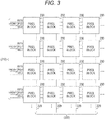
- Fig. 3 is a plan view illustrating a configuration example of the pixel array unit 220 according to the first embodiment of the present technology.
- this pixel array unit 220 a plurality of pixel blocks 230 are laid out in a two-dimensional lattice pattern.
- Each pixel block 230 is provided with a plurality of pixels (e.g., eight pixels).
- block row a group of pixel blocks 230 laid out in a predetermined direction (e.g., horizontal direction)
- a group of pixel blocks 230 laid out in a direction perpendicular to the block row is referred to as "block column”.
- ten horizontal signal lines are wired for each block row and one vertical signal line 229 is wired for each block column.
- One of the ten horizontal signal lines for each row transmits a reset signal RSTi (i is an integer from 0 to I - 1), another one thereof transmits a selection signal SELi, and the remaining eight signal lines transmit transfer signals TRGi0 to TRGi7.
- the horizontal signal line is connected to the pixel blocks 230 in the corresponding block row and the row scan circuit 210. Meanwhile, the vertical signal line 229 is connected to the pixel blocks 230 in the corresponding block column and the AD conversion unit 260.
- Fig. 4 is a circuit diagram illustrating a configuration example of the pixel block 230 according to the first embodiment of the present technology.
- This pixel block 230 includes transfer transistors 231, 232, 235, 236, 242, 243, 247, and 248 and photoelectric conversion devices 233, 234, 237, 238, 245, 246, 249, and 250.
- the pixel block 230 further includes a reset transistor 239, a floating diffusion layer 240, an amplification transistor 241, and a selection transistor 244.
- the photoelectric conversion devices 233, 234, 237, 238, 245, 246, 249, and 250 photoelectrically convert incident light to generate charges. These photoelectric conversion devices are connected to mutually different transfer transistors.
- the transfer transistors 231, 232, 235, 236, 242, 243, 247 and 248 transfer charges from the corresponding photoelectric conversion devices to the floating diffusion layer 240 in accordance with the transfer signals TRGi0 to TRGi7.
- the floating diffusion layer 240 accumulates the charges to generate a voltage according to the amount of accumulated charges.
- the reset transistor 239 sweeps the charges in the floating diffusion layer 240 to the power supply in accordance with the reset signal RSTi to initialize the amount of charges.
- the amplification transistor 241 amplifies a signal of the voltage from the floating diffusion layer 240.
- the selection transistor 244 outputs the signal amplified by the amplification transistor 241 to the vertical signal line 229 as a pixel signal in accordance with the selection signal SELi.
- the row scan circuit 210 sequentially selects rows of pixels and supplies the reset signal RSTi corresponding to the selected row to start exposure of the row. Furthermore, the row scan circuit 210 supplies the selection signal SELi corresponding to the selected row. Then, when the set exposure time has elapsed, the row scan circuit 210 supplies the corresponding transfer signal TRG0i to terminate the exposure. Each exposure action for the row is started when a certain period of time has elapsed from the previous row.
- the row scan circuit 210 sequentially selects block rows and supplies the reset signal RSTi corresponding to the selected block row, to start exposure of the block row. Furthermore, the row scan circuit 210 supplies the selection signal SELi corresponding to the selected block row. Then, when the set exposure time has elapsed, the row scan circuit 210 supplies the transfer signal TRG0i corresponding to the selected block row, to terminate the exposure. Each exposure action for the block row is started when a certain period of time has elapsed from the previous block row. Through this control, pixel addition is performed in units of the pixel block 230 (eight pixels).
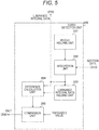
- Fig. 5 is a block diagram illustrating a configuration example of the event detection unit 280 according to the first embodiment of the present technology.
- This event detection unit 280 includes a weight holding unit 281, an integration unit 282, a luminance integral data holding unit 283, a difference calculation unit 284, and a comparison unit 285.
- the weight holding unit 281 holds a weight for multiplying one piece of the addition data for each piece of the addition data. For example, a weight having a larger value than those of the surroundings is set for a piece of the addition data near the center. Photometry with such setting is called center-weighted metering. Note that the imaging apparatus 100 may perform photometry of a technique other than the center-weighted metering, such as multi-zone metering or spot metering.
- the integration unit 282 integrates the M pieces of addition data.
- the integration unit 282 reads the weights from the weight holding unit 281 and performs weighted addition according to the settings of the user.
- the integration unit 282 supplies data subjected to the weighted addition as luminance integral data to the difference calculation unit 284, the luminance integral data holding unit 283, and the exposure control unit 270.
- the luminance integral data holding unit 283 holds the luminance integral data as past luminance integral data.
- the difference calculation unit 284 calculates a difference between the current luminance integral data from the integration unit 282 and the past luminance integral data from the luminance integral data holding unit 283. The difference calculation unit 284 supplies the calculated difference to the comparison unit 285.
- the comparison unit 285 compares the difference with a predetermined threshold value. This comparison unit 285 supplies the comparison result to the mode control unit 290 as a detection result DET. For example, in a case where the difference exceeds the threshold value, it is detected that there has been movement in the subject (in other words, there has been an event) and, in a case where the difference does not exceed the threshold value, it is detected that there is no movement in the subject.
- the comparison unit 285 is an example of a movement detection unit described in the claims.
- the weight holding unit 281 and the integration unit 282 are arranged in the event detection unit 280, these members may be arranged in the exposure control unit 270.
- the event detection unit 280 receives the luminance integral data from the exposure control unit 270.
- the event detection unit 280 detects the presence or absence of movement of the subject from the difference between the current luminance integral data and the past luminance integral data
- the event detection unit 280 is not limited to this configuration.
- the event detection unit 280 may detect the presence or absence of movement of the subject using a background subtraction method in which M pieces of the addition data are acquired as a frame without integrating these pieces of the addition data and compared with a background frame, or a frame subtraction method in which past frames and the current frame are compared, or the like.
- the event detection unit 280 detects the movement of the subject as an event
- the event to be detected is not limited to the movement of the subject as long as the event can be detected using the addition data.
- the event detection unit 280 may perform image recognition to detect the presence or absence of a specific object such as a person.
- the mode control unit 290 may shift the mode to the pixel addition mode when the event detection unit 280 detects that there is no movement in the imaging apparatus 100.
- the event detection unit 280 may focus on a part of the image instead of the entire image to detect the presence or absence of a change in this part of the image.
- the event detection unit 280 may detect the presence or absence of a change in a specific color by integrating luminance data for each color.
- the event detection unit 280 may work out the moving speed of a moving body by the background subtraction method, the frame subtraction method, or the like, to detect whether or not the worked-out speed exceeds a certain speed.
- Fig. 6 is a block diagram illustrating a configuration example of the mode control unit 290 according to the first embodiment of the present technology.
- This mode control unit 290 includes a mode signal generation unit 291 and a counter 292.
- the counter 292 counts a counter value CNT in synchronization with the vertical synchronization signal VSYNC. Furthermore, the counter 292 alters the counter value CNT to an initial value in accordance with the reset signal RST.
- the mode signal generation unit 291 generates the mode signal MODE on the basis of the detection result DET and the counter value CNT. This mode signal generation unit 291 supplies the generated mode signal MODE to the row scan circuit 210 and the switch 213.
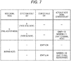
- Fig. 7 is a diagram illustrating an example of the action of the mode signal generation unit 291 according to the first embodiment of the present technology.
- the mode signal MODE for example, "0" is set in the pixel addition mode and "1" is set in the normal mode.
- the detection result DET for example, "0" is set in a case where there is no event and "1" is set in a case where an event occurs.
- the mode signal generation unit 291 sets "1" (normal mode) to the mode signal MODE and initializes the counter value CNT to "0".
- the mode signal generation unit 291 sets "0" (pixel addition mode) to the mode signal MODE.
- the solid-state imaging device 200 shifts from the normal mode to the pixel addition mode when the counter value CNT is N (in other words, when N images are captured), but the solid-state imaging device 200 may shift to the pixel addition mode by a trigger signal from a microcomputer or the like outside the solid-state imaging device 200, instead of the number of captured images.
- This trigger signal is generated, for example, according to an analysis result for an image captured in the normal mode, an operation by the user, or the like.
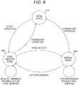
- Fig. 8 is an example of a state transition diagram of the imaging apparatus 100 according to the first embodiment of the present technology.
- the state of the imaging apparatus 100 is classified into three states, namely, an initial state 610, a pixel addition mode 620, and a normal mode 630.
- the initial state 610 is a state in which the solid-state imaging device 200 is stopped
- the pixel addition mode 620 is a state in which the solid-state imaging device 200 is working and performs pixel addition.
- the normal mode 630 is a state in which the solid-state imaging device 200 is working and performs imaging without pixel addition.
- the imaging apparatus 100 causes the solid-state imaging device 200 to work and shifts to the pixel addition mode 620.
- the imaging apparatus 100 acquires the luminance integral data by pixel addition in synchronization with the vertical synchronization signal VSYNC. Then, the imaging apparatus 100 detects the presence or absence of an event from this luminance integral data. In a case where an event occurs, the imaging apparatus 100 shifts to the normal mode 630.
- the imaging apparatus 100 captures image data without pixel addition and, after capturing N images, shifts to the pixel addition mode 620. Furthermore, in the pixel addition mode 620 and the normal mode 630, when a predetermined termination operation for terminating the application is made, the imaging apparatus 100 stops the solid-state imaging device 200 and shifts to the initial state 610.
- Fig. 9 is a block diagram illustrating a configuration example of the AD conversion unit 260 according to the first embodiment of the present technology.
- this AD conversion unit 260 an AD converter 261 is provided for each block column.
- the AD converter 261 acquires analog signals from the corresponding block column via the vertical signal line 229 and performs AD conversion in synchronization with a predetermined clock signal CLK. This AD converter 261 outputs the data subjected to the AD conversion to the switch 213 under the control of the column scan circuit 212.
- Fig. 10 is a block diagram illustrating a configuration example of the DSP circuit 120 according to the first embodiment of the present technology.
- This DSP circuit 120 includes a demosaic processing unit 121 and a post-stage processing unit 122.
- the demosaic processing unit 121 performs a demosaic process on the RAW image data from the solid-state imaging device 200.
- the demosaic process is a process of interpolating a missing color out of the colors of red (R), green (G), and blue (B) from the periphery of each pixel.
- the demosaic processing unit 121 supplies image data after the demosaic process to the post-stage processing unit 122 as YC image data.
- the post-stage processing unit 122 executes a variety of image processes such as a white balance process and a filter process on the YC image data. This post-stage processing unit 122 outputs the processed YC image data to the display unit 130 and the recording unit 170 via the bus 150.
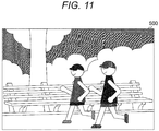
- Fig. 11 is a diagram illustrating an example of a subject image 500 according to the first embodiment of the present technology. As exemplified in Fig. 11 , running persons appear as subjects.
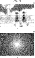
- Fig. 12 is a diagram illustrating an example of a distribution of the addition data and the weights according to the first embodiment of the present technology.
- a illustrates an example of luminance distribution data 510 made up of M pieces of the addition data generated from the subject image 500.
- b illustrates an example of a distribution of the weights.
- each of sections delimited by dotted lines in Fig. 12 indicates an area corresponding to the pixel block.
- the solid-state imaging device 200 generates the addition data from the addition signal of one pixel block for each pixel block.
- addition data B00 is generated from the addition signal of the upper left pixel block
- addition data B01 and addition data B10 are generated from the addition signals of two pixel blocks adjacent to the upper left pixel block.
- the luminance integral data is calculated by weighted addition between the addition data and the weight corresponding to this addition data.
- the addition data B00 is multiplied by a corresponding weight W00.
- the addition data B01 is multiplied by a weight W01 and the addition data B10 is multiplied by a weight W10.
- Fig. 13 is a timing chart illustrating an example of the action of the solid-state imaging device 200 in the pixel addition mode according to the first embodiment of the present technology. It is assumed that the pixel addition mode is set at a timing T0.
- the row scan circuit 210 controls the reset signal RST0 corresponding to a zeroth block row to a high level over a predetermined pulse period. With this control, the exposure of the zeroth block row is started. Then, at a timing T1 when a certain exposure time has elapsed, the row scan circuit 210 controls all of the transfer signals TRG00 to TRG07 corresponding to the zeroth block row to an ON state over the pulse period. With this control, the exposure of the zeroth block row is terminated.
- the row scan circuit 210 controls the selection signal SEL0 corresponding to the zeroth block row to the ON state during a period from the timing T0 to a timing T2. With this control, the addition signal of the zeroth block row is read.
- exposure and reading of the first and subsequent block rows are sequentially executed.
- exposure and reading are started when a certain period of time has elapsed since exposure and reading of the previous block row. Then, reading of all the block rows is executed a plurality of times in synchronization with the vertical synchronization signal VSYNC.
- Fig. 14 is a timing chart illustrating an example of the action of the solid-state imaging device 200 in the normal mode according to the first embodiment of the present technology. It is assumed that an event is detected and the normal mode is set at a timing T10 after the timing T0.
- the row scan circuit 210 controls the reset signal RST0 corresponding to a zeroth row of pixels to a high level over a predetermined pulse period. With this control, the exposure of some pixels in the zeroth row is started. Then, at a timing T11 when a certain exposure time has elapsed, the row scan circuit 210 controls the transfer signal TRG00 corresponding to the zeroth row to an ON state over the pulse period. With this control, the exposure of the some pixels in the zeroth row is terminated.
- the row scan circuit 210 again controls the reset signal RST0 to the high level over the predetermined pulse period and, at a timing T13 after the exposure period elapses, controls the transfer signal TRG01 to the ON state over the pulse period. With this control, the remaining pixels in the zeroth row are exposed.
- the row scan circuit 210 controls the selection signal SEL0 corresponding to the zeroth to third rows to the ON state during a period from the timing T0 until when these rows are read.
- exposure and reading of the first and subsequent rows are sequentially executed.
- exposure and reading are started when a certain period of time has elapsed since exposure and reading of the previous row. Then, reading of all the rows is executed a plurality of times in synchronization with the vertical synchronization signal VSYNC.
- Fig. 15 is a flowchart illustrating an example of the action of the imaging apparatus 100 according to the first embodiment of the present technology. This action starts, for example, when a predetermined application is executed.
- the imaging apparatus 100 shifts to the pixel addition mode (step S901) and acquires the luminance integral data by pixel addition (step S902). Then, on the basis of the acquired luminance integral data, the imaging apparatus 100 determines whether or not a predetermined event has occurred (step S903). In a case where no event has occurred (step S903: No), the imaging apparatus 100 repeatedly executes step S902 and the subsequent steps.
- step S903 Yes
- the imaging apparatus 100 shifts to the normal mode and initializes the counter value CNT to "0" (step S904). Then, the imaging apparatus 100 captures the image data without pixel addition and increments the counter value CNT (step S905). The imaging apparatus 100 determines whether or not the counter value CNT is equal to or greater than N (step S906). In a case where the counter value CNT is less than N (step S906: No), the imaging apparatus 100 repeatedly executes step S905 and the subsequent steps.
- step S906 Yes
- the imaging apparatus 100 repeatedly executes step S901 and the subsequent steps.
- the solid-state imaging device 200 since the solid-state imaging device 200 generates the addition data by pixel addition until an event is detected, it is possible to reduce the power consumption as compared with a case where imaging is always performed without pixel addition.
- the solid-state imaging device 200 performs exposure control and event detection.
- a configuration in which these processes are performed by a member outside the solid-state imaging device 200 e.g., the DSP circuit 120
- Such an imaging apparatus 100 according to a second embodiment is different from that of the first embodiment in that exposure control and event detection are performed by a circuit outside a solid-state imaging device 200.
- Fig. 16 is a block diagram illustrating a configuration example of the solid-state imaging device 200 according to the second embodiment of the present technology.
- This solid-state imaging device 200 of the second embodiment is different from that of the first embodiment in that the solid-state imaging device 200 does not include the switch 213, the exposure control unit 270, the event detection unit 280, and the mode control unit 290.
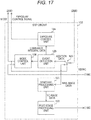
- Fig. 17 is a block diagram illustrating a configuration example of a DSP circuit 120 according to the second embodiment of the present technology.
- This DSP circuit 120 of the second embodiment is different from that of the first embodiment in that the DSP circuit 120 further includes a switch 123, an exposure control unit 124, an event detection unit 125, and a mode control unit 126.
- the switch 123, the exposure control unit 124, the event detection unit 125, and the mode control unit 126 in the DSP circuit 120 have similar configurations to those of the switch 213, the exposure control unit 270, the event detection unit 280, and the mode control unit 290 of the first embodiment. Note that, although the exposure control unit 124, the event detection unit 125, and the mode control unit 126 are arranged in the DSP circuit 120, these members may be arranged in a circuit other than the DSP circuit 120 as long as the circuit is located outside the solid-state imaging device 200.
- the processing amount of the solid-state imaging device 200 can be lessened as compared with a case where these members are provided in the solid-state imaging device 200.
- a previously set area e.g., an area near the center
- intensively photometered e.g., an area near the center
- an appropriate photometric amount cannot be obtained.
- Such an imaging apparatus 100 according to a third embodiment is different from that of the first embodiment in that an area where the subject has moved is intensively photometered.
- Fig. 18 is a block diagram illustrating a configuration example of an event detection unit 280 according to the third embodiment of the present technology.
- This event detection unit 280 according to the third embodiment is different from that of the first embodiment in that the event detection unit 280 further includes an addition data holding unit 286, a difference calculation unit 287, and a weight holding unit 288.
- the addition data holding unit 286 holds M pieces of the addition data as past addition data.
- the difference calculation unit 287 calculates a difference between the current addition data from the switch 213 and the corresponding addition data in the addition data holding unit 286 for each pixel block. In a case where the number of pixel blocks is M, M differences are calculated. The difference calculation unit 287 generates a weight having a larger value as the difference is larger (in different terms, the movement is larger) for each pixel block, and holds the generated weight in the weight holding unit 288. The weight holding unit 288 holds the weight generated by the difference calculation unit 287. Note that the difference calculation unit 287 is an example of a difference acquisition unit described in the claims.
- an integration unit 282 of the third embodiment performs weighted addition according to the weight in the weight holding unit 281 in the first photometry, and performs weighted addition according to the weight in the weight holding unit 288 in the second and subsequent photometry.
- Fig. 19 is a diagram illustrating an example of a distribution of the weights according to the third embodiment of the present technology.
- the bright area indicates an area where the subject has moved.
- the imaging apparatus 100 sets the weight (such as W24) of the area where the subject has moved to a value larger than the weights (such as W00) of the other areas. With this setting, the imaging apparatus 100 can intensively photometer the area where the subject has moved, and control the exposure amount to an appropriate amount.
- the imaging apparatus 100 since the imaging apparatus 100 performs weighted addition using the weight according to the difference between the current addition data and the past addition data, it is possible to intensively photometer an area where the subject has moved.
- the process procedures described in the above embodiments may be regarded as a method having these series of procedures and additionally, may be regarded as a program for causing a computer to execute these series of procedures or as a recording medium storing the program.
- this recording medium for example, a compact disc (CD), a mini disc (MD), a digital versatile disc (DVD), a memory card, a Blu-ray (registered trademark) disc, or the like can be used.
Landscapes
- Engineering & Computer Science (AREA)
- Multimedia (AREA)
- Signal Processing (AREA)
- Physics & Mathematics (AREA)
- General Physics & Mathematics (AREA)
- Theoretical Computer Science (AREA)
- Transforming Light Signals Into Electric Signals (AREA)
- Studio Devices (AREA)
Abstract
Description
- The present technology relates to an imaging apparatus and a control method for the imaging apparatus. In detail, the present technology relates to an imaging apparatus and a control method for the imaging apparatus that detect the presence or absence of an event such as movement of a subject.
- Conventionally, imaging apparatuses that detect the presence or absence of an event such as movement of a subject by an image process are widely utilized in fields such as measurement, traffic, and crime prevention. For example, there has been proposed an imaging apparatus that captures a plurality of pieces of image data (frames) at a constant imaging interval and detects the presence or absence of an event from a difference between the integral value of the luminance of the current frame and the integral value of the luminance of the past frame (see, for example, Patent Document 1). This imaging apparatus is used for, for example, an application that does not record a frame in a memory until an event occurs and starts recording of a frame when an event occurs to save the memory capacity, or the like.
- Patent Document 1: Japanese Patent Application Laid-Open No.
2004-274533 - In the imaging apparatus described above, from the viewpoint of enhancing the image quality of the frame, frames are captured without pixel addition before and after the event detection. However, when imaging is performed without pixel addition, there is a difficulty that the number of times of analog-to-digital (AD) conversion increases and the power consumption grows large as compared with the case of pixel addition. If the resolution of the frame is lowered by pixel addition, the number of times of AD conversion can be made smaller to reduce power consumption, but it is undesirable because the image quality of the frame to be recorded after event detection deteriorates.
- The present technology has been created in view of such a situation and it is an object of the present technology to reduce power consumption in an imaging apparatus that detects the presence or absence of an event.
- The present technology has been made in order to eliminate the above-mentioned difficulties and a first aspect thereof is an imaging apparatus and a control method therefor, the imaging apparatus including: a pixel array unit provided with a plurality of transfer transistors that transfer the charges from mutually different photoelectric conversion devices to a floating diffusion layer; a scan circuit that simultaneously controls the plurality of transfer transistors in a pixel addition mode in which pixel addition is performed, to transfer the charges, and sequentially controls the plurality of transfer transistors in a normal mode in which pixel addition is not performed, to transfer the charges; an event detection unit that detects presence or absence of a predetermined event on the basis of an addition signal which is an analog signal generated in the pixel addition mode, and generates a detection result; and a mode control unit that sets one of the pixel addition mode and the normal mode on the basis of the detection result. This brings about effectiveness that one of the pixel addition mode and the normal mode is set on the basis of the detection result for the event.
- Furthermore, in this first aspect, an analog-to-digital conversion unit that performs analog-to-digital conversion on the addition signal to output as addition data may be further included. This brings about effectiveness that the addition signal is subjected to the analog-to-digital conversion.
- Furthermore, in this first aspect, a predetermined number of the floating diffusion layers may be arranged in the pixel array unit, and an exposure control unit that controls an exposure amount of the pixel array unit on the basis of luminance integral data obtained by integrating the predetermined number of pieces of the addition data may be further included. This brings about effectiveness that the exposure amount is controlled on the basis of the luminance integral data.
- Furthermore, in this first aspect, the event detection unit may detect presence or absence of movement of a subject as presence or absence of the predetermined event. This brings about effectiveness that one of the pixel addition mode and the normal mode is set on the basis of a detection result for the presence or absence of movement of the subject.
- Furthermore, in this first aspect, the event detection unit may include: a luminance integral data holding unit that holds the luminance integral data as past integral data; and a movement detection unit that detects presence or absence of movement of the subject depending on whether or not a difference between new luminance integral data and the past integral data exceeds a predetermined threshold value. This brings about effectiveness that the presence or absence of movement of the subject is detected depending on the difference between the new luminance integral data and the past integral data.
- Furthermore, in this first aspect, the event detection unit may further include: an addition data holding unit that holds the predetermined number of pieces of addition data as past addition data; and a difference acquisition unit that acquires a difference between new addition data and the past addition data corresponding to the new addition data and generates a weight according to the difference, and the luminance integral data may be a weighted addition value of the addition data and the weight corresponding to the addition data. This brings about effectiveness that the exposure amount is controlled on the basis of the weighted addition value of the addition data and the weight corresponding to the addition data.
- Furthermore, in this first aspect, the pixel array unit may generate an image signal including the analog signal in the normal mode, and the mode control unit may set the normal mode in a case where it is detected that the predetermined event has occurred, and may set the pixel addition mode in a case where a certain number of the image signals are generated. This brings about effectiveness that the pixel addition mode is set in a case where a certain number of image signals are generated.
- Furthermore, in this first aspect, the pixel array unit, the scan circuit, the event detection unit, and the mode control unit may be arranged in a solid-state imaging device. This brings about effectiveness that an event is detected by the solid-state imaging device.
- Furthermore, in this first aspect, the pixel array unit and the scan circuit may be arranged in a solid-state imaging device, and the event detection unit and the mode control unit may be arranged outside the solid-state imaging device. This brings about effectiveness that an event is detected outside the solid-state imaging device.
- According to the present technology, it is possible to achieve an excellent effect that the power consumption can be reduced in an imaging apparatus that detects the presence or absence of an event. Note that the effects described herein are not necessarily limited and any effects described in the present disclosure may be applied.
-
-
Fig. 1 is a block diagram illustrating a configuration example of an imaging apparatus according to a first embodiment of the present technology. -
Fig. 2 is a block diagram illustrating a configuration example of a solid-state imaging device according to the first embodiment of the present technology. -
Fig. 3 is a plan view illustrating a configuration example of a pixel array unit according to the first embodiment of the present technology. -
Fig. 4 is a circuit diagram illustrating a configuration example of a pixel block according to the first embodiment of the present technology. -
Fig. 5 is a block diagram illustrating a configuration example of an event detection unit according to the first embodiment of the present technology. -
Fig. 6 is a block diagram illustrating a configuration example of a mode control unit according to the first embodiment of the present technology. -
Fig. 7 is a diagram illustrating an example of the action of a mode signal generation unit according to the first embodiment of the present technology. -
Fig. 8 is an example of a state transition diagram of the imaging apparatus according to the first embodiment of the present technology. -
Fig. 9 is a block diagram illustrating a configuration example of an AD conversion unit according to the first embodiment of the present technology. -
Fig. 10 is a block diagram illustrating a configuration example of a digital signal processing (DSP) circuit according to the first embodiment of the present technology. -
Fig. 11 is a diagram illustrating an example of a subject image according to the first embodiment of the present technology. -
Fig. 12 is a diagram illustrating an example of a distribution of addition data and weights according to the first embodiment of the present technology. -
Fig. 13 is a timing chart illustrating an example of the action of the solid-state imaging device in a pixel addition mode according to the first embodiment of the present technology. -
Fig. 14 is a timing chart illustrating an example of the action of the solid-state imaging device in a normal mode according to the first embodiment of the present technology. -
Fig. 15 is a flowchart illustrating an example of the action of the imaging apparatus according to the first embodiment of the present technology. -
Fig. 16 is a block diagram illustrating a configuration example of a solid-state imaging device according to a second embodiment of the present technology. -
Fig. 17 is a block diagram illustrating a configuration example of a DSP circuit according to the second embodiment of the present technology. -
Fig. 18 is a block diagram illustrating a configuration example of an event detection unit according to a third embodiment of the present technology. -
Fig. 19 is a diagram illustrating an example of a distribution of weights according to the third embodiment of the present technology. - Modes for carrying out the present technology (hereinafter, referred to as embodiments) will be described below. The description will be given in the following order.
- 1. First Embodiment (an example in which pixel addition is performed until an event is detected)
- 2. Second Embodiment (an example in which pixel addition is performed until an event is detected by a DSP circuit)
- 3. Third Embodiment (an example in which pixel addition is performed until an event is detected and an area where a subject has moved is intensively photometered)
-
Fig. 1 is a block diagram illustrating a configuration example of animaging apparatus 100 according to a first embodiment of the present technology. Thisimaging apparatus 100 includes anoptical unit 110, a solid-state imaging device 200, aDSP circuit 120, adisplay unit 130, anoperation unit 140, abus 150, apower supply unit 160, arecording unit 170, and aframe memory 180. As theimaging apparatus 100, an information processing apparatus or a smartphone having an imaging function, a digital camera, or the like is supposed. - The
optical unit 110 collects incident light from a subject and guides the collected incident light to the solid-state imaging device 200. Theoptical unit 110 is constituted by, for example, a plurality of lenses, a diaphragm, a shutter, and the like. - The solid-
state imaging device 200 photoelectrically converts incident light to capture image data. This solid-state imaging device 200 supplies the generated image data (frame) to theDSP circuit 120. - The
DSP circuit 120 executes a predetermined digital signal process on the frame from the solid-state imaging device 200. For example, a variety of digital signal processes including a demosaic process, a white balance process, a filter process, and the like are executed. In these processes, theDSP circuit 120 causes theframe memory 180 to hold the frame as necessary. Then, theDSP circuit 120 outputs the processed frame to thedisplay unit 130 and therecording unit 170. - The
display unit 130 displays a frame or the like. Theoperation unit 140 generates an operation signal in accordance with a user's operation. - The
bus 150 is a common path through which the solid-state imaging device 200, theDSP circuit 120, thedisplay unit 130, theoperation unit 140, thepower supply unit 160, therecording unit 170, and theframe memory 180 exchange data with each other. - The
power supply unit 160 supplies power to a circuit in theimaging apparatus 100. Therecording unit 170 records a frame. Theframe memory 180 holds a frame. - Note that, although the
optical unit 110, the solid-state imaging device 200, theDSP circuit 120, thedisplay unit 130, theoperation unit 140, thebus 150, thepower supply unit 160, therecording unit 170, and theframe memory 180 are provided in the same apparatus, these members may be provided in a plurality of apparatuses in a dispersed manner. For example, theoptical unit 110 and the solid-state imaging device 200 may be arranged in the imaging apparatus, while theDSP circuit 120 and the like may be arranged in an information processing apparatus. -
Fig. 2 is a block diagram illustrating a configuration example of the solid-state imaging device 200 according to the first embodiment of the present technology. This solid-state imaging device 200 includes arow scan circuit 210, apixel array unit 220, atiming control unit 211, anAD conversion unit 260, acolumn scan circuit 212, aswitch 213, anexposure control unit 270, anevent detection unit 280, and amode control unit 290. - Furthermore, in the
pixel array unit 220, a plurality of pixels is laid out in a two-dimensional lattice pattern. Hereinafter, a group of pixels laid out in a predetermined direction (e.g., horizontal direction) is referred to as "row" and a group of pixels laid out in a direction perpendicular to the row is referred to as "column". - The
timing control unit 211 controls action timings of therow scan circuit 210, theAD conversion unit 260, and thecolumn scan circuit 212. A vertical synchronization signal VSYNC of a predetermined frequency fVSYNC (e.g., 30 hertz) is input to thistiming control unit 211 via thebus 150. This vertical synchronization signal VSYNC is generated by a phase locked loop (not illustrated), theDSP circuit 120, or the like. - The
timing control unit 211 generates timing signals indicating the respective action timings of therow scan circuit 210, theAD conversion unit 260, and thecolumn scan circuit 212 in synchronization with the vertical synchronization signal VSYNC and supplies the corresponding timing signals to each member. - The
row scan circuit 210 drives the pixel to generate an analog signal at a level according to the exposure amount. An exposure control signal and a mode signal MODE are input to thisrow scan circuit 210. The exposure control signal is a signal for controlling the exposure time. Meanwhile, the mode signal MODE is a signal indicating one of a pixel addition mode in which pixel addition is performed or a normal mode in which pixel addition is not performed. - In the pixel addition mode, the
row scan circuit 210 controls thepixel array unit 220 to generate an analog addition signal by pixel addition. Meanwhile, in the normal mode, therow scan circuit 210 controls thepixel array unit 220 to generate an analog pixel signal for each pixel. Note that therow scan circuit 210 is an example of a scan circuit described in the claims. - The
AD conversion unit 260 performs AD conversion on the analog signal (the addition signal or the pixel signal) from thepixel array unit 220. TheAD conversion unit 260 performs AD conversion on the addition signal to generate addition data and performs AD conversion on the pixel signal to generate pixel data. Then, theAD conversion unit 260 supplies the generated data (the addition data or the pixel data) to theswitch 213. - Here, the number of pieces of the addition data generated within the cycle of 1/fVSYNC is defined by the resolution and an addition unit of the image data. For example, in a case where the number of rows is I, the number of columns is J, and addition is performed every eight pixels, the number M of pieces of the addition data generated within an imaging interval T (= 1/fVSYNC) is expressed by the following formula. Here, I, J and M are integers. Note that the addition unit is not limited to eight pixels and may be four pixels or the like.

- The
switch 213 switches the output destination of the data from theAD conversion unit 260 in accordance with the mode signal MODE. In the pixel addition mode, thisswitch 213 supplies the addition data from theAD conversion unit 260 to theevent detection unit 280. Meanwhile, in the normal mode, theswitch 213 supplies image data including the pixel data from theAD conversion unit 260 to theDSP circuit 120 as RAW image data. - The
event detection unit 280 detects the presence or absence of a predetermined event on the basis of the addition data to generate a detection result DET. For example, the movement of the subject is detected as an event. Furthermore, theevent detection unit 280 integrates the M pieces of addition data to supply to theexposure control unit 270 as luminance integral data. This luminance integral data indicates the photometric amount of the entire image. - The
exposure control unit 270 controls the exposure amount of thepixel array unit 220 on the basis of the luminance integral data (photometric amount). Thisexposure control unit 270 translates the luminance integral data into an exposure value EV and works out the exposure time, for example, by the following formula. Then, theexposure control unit 270 generates an exposure control signal for controlling the exposure time to the worked-out time and supplies the generated exposure control signal to therow scan circuit 210.
- In the above formula, AV represents the logarithm of the F value and TV represents the logarithm of the exposure time.
- Note that, although the
exposure control unit 270 controls the exposure time, the diaphragm may be controlled instead of the exposure time. - The
mode control unit 290 sets one of the pixel addition mode and the normal mode. When a predetermined operation is made by the user, thismode control unit 290 first sets the mode signal MODE with the pixel addition mode. This mode signal MODE is supplied to therow scan circuit 210 and theswitch 213. - Then, when a predetermined event occurs during the set pixel addition mode, the
mode control unit 290 sets the mode signal MODE with the normal mode. Next, when a certain number of pieces of image data is captured during the normal mode, themode control unit 290 sets the mode signal MODE with the pixel addition mode. - As described earlier, in the normal mode, since AD conversion is performed for each pixel, the number of times of AD conversion is obtained by I × J times. On the other hand, in the pixel addition mode, AD conversion is performed for every addition unit of pixel addition. Therefore, the number of times of AD conversion required in the case of addition every eight pixels is only (M × N)/8 times. Furthermore, in the normal mode, an image process is executed by the
DSP circuit 120 at the post stage but, in the pixel addition mode, the addition data is not output to theDSP circuit 120 and the image process is not performed. Since the number of times of AD conversion is small and the processing amount for image process is decreased as described above, the power consumption of theimaging apparatus 100 in the pixel addition mode is reduced as compared with the normal mode. - Then, the
imaging apparatus 100 works in the pixel addition mode until an event is detected and shifts to the normal mode when an event is detected. For this reason, the power consumption of theimaging apparatus 100 can be reduced as compared with a case where theimaging apparatus 100 always works without pixel addition (in other words, in the normal mode) regardless of the presence or absence of an event. - For example, it is assumed that the power consumption in the pixel addition mode is 1.5 milliwatts (mW) per hour and the power consumption in the normal mode is 34.8 milliwatts (mW) per hour. Furthermore, it is assumed that the frequency fVSYNC of the vertical synchronization signal VSYNC is 30 hertz (Hz) and 60 pieces of image data are captured in one hour in the normal mode. In this case, the power consumption of the
imaging apparatus 100 per hour can be worked out by the following formula.
- In this manner, compared with the value (34.8 mW) in the case of working always in the normal mode, the power consumption can be greatly reduced.
-
Fig. 3 is a plan view illustrating a configuration example of thepixel array unit 220 according to the first embodiment of the present technology. In thispixel array unit 220, a plurality of pixel blocks 230 are laid out in a two-dimensional lattice pattern. Eachpixel block 230 is provided with a plurality of pixels (e.g., eight pixels). - Hereinafter, a group of pixel blocks 230 laid out in a predetermined direction (e.g., horizontal direction) is referred to as "block row" and a group of pixel blocks 230 laid out in a direction perpendicular to the block row is referred to as "block column".
- Furthermore, ten horizontal signal lines are wired for each block row and one
vertical signal line 229 is wired for each block column. One of the ten horizontal signal lines for each row transmits a reset signal RSTi (i is an integer from 0 to I - 1), another one thereof transmits a selection signal SELi, and the remaining eight signal lines transmit transfer signals TRGi0 to TRGi7. - The horizontal signal line is connected to the pixel blocks 230 in the corresponding block row and the
row scan circuit 210. Meanwhile, thevertical signal line 229 is connected to the pixel blocks 230 in the corresponding block column and theAD conversion unit 260. -
Fig. 4 is a circuit diagram illustrating a configuration example of thepixel block 230 according to the first embodiment of the present technology. Thispixel block 230 includestransfer transistors photoelectric conversion devices pixel block 230 further includes areset transistor 239, a floatingdiffusion layer 240, anamplification transistor 241, and aselection transistor 244. - The
photoelectric conversion devices - The
transfer transistors diffusion layer 240 in accordance with the transfer signals TRGi0 to TRGi7. The floatingdiffusion layer 240 accumulates the charges to generate a voltage according to the amount of accumulated charges. - The
reset transistor 239 sweeps the charges in the floatingdiffusion layer 240 to the power supply in accordance with the reset signal RSTi to initialize the amount of charges. - The
amplification transistor 241 amplifies a signal of the voltage from the floatingdiffusion layer 240. Theselection transistor 244 outputs the signal amplified by theamplification transistor 241 to thevertical signal line 229 as a pixel signal in accordance with the selection signal SELi. - In the normal mode, the
row scan circuit 210 sequentially selects rows of pixels and supplies the reset signal RSTi corresponding to the selected row to start exposure of the row. Furthermore, therow scan circuit 210 supplies the selection signal SELi corresponding to the selected row. Then, when the set exposure time has elapsed, therow scan circuit 210 supplies the corresponding transfer signal TRG0i to terminate the exposure. Each exposure action for the row is started when a certain period of time has elapsed from the previous row. - Meanwhile, in the pixel addition mode, the
row scan circuit 210 sequentially selects block rows and supplies the reset signal RSTi corresponding to the selected block row, to start exposure of the block row. Furthermore, therow scan circuit 210 supplies the selection signal SELi corresponding to the selected block row. Then, when the set exposure time has elapsed, therow scan circuit 210 supplies the transfer signal TRG0i corresponding to the selected block row, to terminate the exposure. Each exposure action for the block row is started when a certain period of time has elapsed from the previous block row. Through this control, pixel addition is performed in units of the pixel block 230 (eight pixels). - As described above, in the normal mode, exposure is performed sequentially in units of rows of pixels, whereas in the pixel addition mode, exposure is performed sequentially in units of block rows.
-
Fig. 5 is a block diagram illustrating a configuration example of theevent detection unit 280 according to the first embodiment of the present technology. Thisevent detection unit 280 includes aweight holding unit 281, anintegration unit 282, a luminance integraldata holding unit 283, adifference calculation unit 284, and acomparison unit 285. - The
weight holding unit 281 holds a weight for multiplying one piece of the addition data for each piece of the addition data. For example, a weight having a larger value than those of the surroundings is set for a piece of the addition data near the center. Photometry with such setting is called center-weighted metering. Note that theimaging apparatus 100 may perform photometry of a technique other than the center-weighted metering, such as multi-zone metering or spot metering. - The
integration unit 282 integrates the M pieces of addition data. In the integration, theintegration unit 282 reads the weights from theweight holding unit 281 and performs weighted addition according to the settings of the user. Theintegration unit 282 supplies data subjected to the weighted addition as luminance integral data to thedifference calculation unit 284, the luminance integraldata holding unit 283, and theexposure control unit 270. - The luminance integral
data holding unit 283 holds the luminance integral data as past luminance integral data. - The
difference calculation unit 284 calculates a difference between the current luminance integral data from theintegration unit 282 and the past luminance integral data from the luminance integraldata holding unit 283. Thedifference calculation unit 284 supplies the calculated difference to thecomparison unit 285. - The
comparison unit 285 compares the difference with a predetermined threshold value. Thiscomparison unit 285 supplies the comparison result to themode control unit 290 as a detection result DET. For example, in a case where the difference exceeds the threshold value, it is detected that there has been movement in the subject (in other words, there has been an event) and, in a case where the difference does not exceed the threshold value, it is detected that there is no movement in the subject. Note that thecomparison unit 285 is an example of a movement detection unit described in the claims. - In addition, although the
weight holding unit 281 and theintegration unit 282 are arranged in theevent detection unit 280, these members may be arranged in theexposure control unit 270. In this case, theevent detection unit 280 receives the luminance integral data from theexposure control unit 270. - Furthermore, although the
event detection unit 280 detects the presence or absence of movement of the subject from the difference between the current luminance integral data and the past luminance integral data, theevent detection unit 280 is not limited to this configuration. For example, theevent detection unit 280 may detect the presence or absence of movement of the subject using a background subtraction method in which M pieces of the addition data are acquired as a frame without integrating these pieces of the addition data and compared with a background frame, or a frame subtraction method in which past frames and the current frame are compared, or the like. - Furthermore, although the
event detection unit 280 detects the movement of the subject as an event, the event to be detected is not limited to the movement of the subject as long as the event can be detected using the addition data. For example, theevent detection unit 280 may perform image recognition to detect the presence or absence of a specific object such as a person. - Furthermore, the
mode control unit 290 may shift the mode to the pixel addition mode when theevent detection unit 280 detects that there is no movement in theimaging apparatus 100. Alternatively, theevent detection unit 280 may focus on a part of the image instead of the entire image to detect the presence or absence of a change in this part of the image. In addition, theevent detection unit 280 may detect the presence or absence of a change in a specific color by integrating luminance data for each color. Alternatively, theevent detection unit 280 may work out the moving speed of a moving body by the background subtraction method, the frame subtraction method, or the like, to detect whether or not the worked-out speed exceeds a certain speed. -
Fig. 6 is a block diagram illustrating a configuration example of themode control unit 290 according to the first embodiment of the present technology. Thismode control unit 290 includes a modesignal generation unit 291 and acounter 292. - The
counter 292 counts a counter value CNT in synchronization with the vertical synchronization signal VSYNC. Furthermore, thecounter 292 alters the counter value CNT to an initial value in accordance with the reset signal RST. - The mode
signal generation unit 291 generates the mode signal MODE on the basis of the detection result DET and the counter value CNT. This modesignal generation unit 291 supplies the generated mode signal MODE to therow scan circuit 210 and theswitch 213. -
Fig. 7 is a diagram illustrating an example of the action of the modesignal generation unit 291 according to the first embodiment of the present technology. As the mode signal MODE, for example, "0" is set in the pixel addition mode and "1" is set in the normal mode. Furthermore, in the detection result DET, for example, "0" is set in a case where there is no event and "1" is set in a case where an event occurs. - When the detection result DET becomes "1" (there is an event) while the mode signal MODE is "0" (pixel addition mode), the mode
signal generation unit 291 sets "1" (normal mode) to the mode signal MODE and initializes the counter value CNT to "0". - Furthermore, when the counter value CNT becomes equal to or greater than N (N is an integer) while the mode signal MODE is "1" (normal mode), the mode
signal generation unit 291 sets "0" (pixel addition mode) to the mode signal MODE. Note that the solid-state imaging device 200 shifts from the normal mode to the pixel addition mode when the counter value CNT is N (in other words, when N images are captured), but the solid-state imaging device 200 may shift to the pixel addition mode by a trigger signal from a microcomputer or the like outside the solid-state imaging device 200, instead of the number of captured images. This trigger signal is generated, for example, according to an analysis result for an image captured in the normal mode, an operation by the user, or the like. -
Fig. 8 is an example of a state transition diagram of theimaging apparatus 100 according to the first embodiment of the present technology. The state of theimaging apparatus 100 is classified into three states, namely, aninitial state 610, apixel addition mode 620, and anormal mode 630. Theinitial state 610 is a state in which the solid-state imaging device 200 is stopped, while thepixel addition mode 620 is a state in which the solid-state imaging device 200 is working and performs pixel addition. Furthermore, thenormal mode 630 is a state in which the solid-state imaging device 200 is working and performs imaging without pixel addition. - In the
initial state 610, when a start operation for starting a predetermined application is made, theimaging apparatus 100 causes the solid-state imaging device 200 to work and shifts to thepixel addition mode 620. - In the
pixel addition mode 620, theimaging apparatus 100 acquires the luminance integral data by pixel addition in synchronization with the vertical synchronization signal VSYNC. Then, theimaging apparatus 100 detects the presence or absence of an event from this luminance integral data. In a case where an event occurs, theimaging apparatus 100 shifts to thenormal mode 630. - In the
normal mode 630, theimaging apparatus 100 captures image data without pixel addition and, after capturing N images, shifts to thepixel addition mode 620. Furthermore, in thepixel addition mode 620 and thenormal mode 630, when a predetermined termination operation for terminating the application is made, theimaging apparatus 100 stops the solid-state imaging device 200 and shifts to theinitial state 610. -
Fig. 9 is a block diagram illustrating a configuration example of theAD conversion unit 260 according to the first embodiment of the present technology. In thisAD conversion unit 260, anAD converter 261 is provided for each block column. - The
AD converter 261 acquires analog signals from the corresponding block column via thevertical signal line 229 and performs AD conversion in synchronization with a predetermined clock signal CLK. ThisAD converter 261 outputs the data subjected to the AD conversion to theswitch 213 under the control of thecolumn scan circuit 212. -
Fig. 10 is a block diagram illustrating a configuration example of theDSP circuit 120 according to the first embodiment of the present technology. ThisDSP circuit 120 includes ademosaic processing unit 121 and apost-stage processing unit 122. - The
demosaic processing unit 121 performs a demosaic process on the RAW image data from the solid-state imaging device 200. Here, the demosaic process is a process of interpolating a missing color out of the colors of red (R), green (G), and blue (B) from the periphery of each pixel. Thedemosaic processing unit 121 supplies image data after the demosaic process to thepost-stage processing unit 122 as YC image data. - The
post-stage processing unit 122 executes a variety of image processes such as a white balance process and a filter process on the YC image data. Thispost-stage processing unit 122 outputs the processed YC image data to thedisplay unit 130 and therecording unit 170 via thebus 150. -
Fig. 11 is a diagram illustrating an example of asubject image 500 according to the first embodiment of the present technology. As exemplified inFig. 11 , running persons appear as subjects. -
Fig. 12 is a diagram illustrating an example of a distribution of the addition data and the weights according to the first embodiment of the present technology. InFig. 12 , a illustrates an example ofluminance distribution data 510 made up of M pieces of the addition data generated from thesubject image 500. InFig. 12, b illustrates an example of a distribution of the weights. Furthermore, each of sections delimited by dotted lines inFig. 12 indicates an area corresponding to the pixel block. - The solid-
state imaging device 200 generates the addition data from the addition signal of one pixel block for each pixel block. For example, addition data B00 is generated from the addition signal of the upper left pixel block and addition data B01 and addition data B10 are generated from the addition signals of two pixel blocks adjacent to the upper left pixel block. - Furthermore, a larger value than those of the surroundings is set as the weight near the center. Then, the luminance integral data is calculated by weighted addition between the addition data and the weight corresponding to this addition data. For example, the addition data B00 is multiplied by a corresponding weight W00. The addition data B01 is multiplied by a weight W01 and the addition data B10 is multiplied by a weight W10.
-
Fig. 13 is a timing chart illustrating an example of the action of the solid-state imaging device 200 in the pixel addition mode according to the first embodiment of the present technology. It is assumed that the pixel addition mode is set at a timing T0. - The
row scan circuit 210 controls the reset signal RST0 corresponding to a zeroth block row to a high level over a predetermined pulse period. With this control, the exposure of the zeroth block row is started. Then, at a timing T1 when a certain exposure time has elapsed, therow scan circuit 210 controls all of the transfer signals TRG00 to TRG07 corresponding to the zeroth block row to an ON state over the pulse period. With this control, the exposure of the zeroth block row is terminated. - Furthermore, the
row scan circuit 210 controls the selection signal SEL0 corresponding to the zeroth block row to the ON state during a period from the timing T0 to a timing T2. With this control, the addition signal of the zeroth block row is read. - After the timing T2, exposure and reading of the first and subsequent block rows are sequentially executed. In each block row, exposure and reading are started when a certain period of time has elapsed since exposure and reading of the previous block row. Then, reading of all the block rows is executed a plurality of times in synchronization with the vertical synchronization signal VSYNC.
-
Fig. 14 is a timing chart illustrating an example of the action of the solid-state imaging device 200 in the normal mode according to the first embodiment of the present technology. It is assumed that an event is detected and the normal mode is set at a timing T10 after the timing T0. - The
row scan circuit 210 controls the reset signal RST0 corresponding to a zeroth row of pixels to a high level over a predetermined pulse period. With this control, the exposure of some pixels in the zeroth row is started. Then, at a timing T11 when a certain exposure time has elapsed, therow scan circuit 210 controls the transfer signal TRG00 corresponding to the zeroth row to an ON state over the pulse period. With this control, the exposure of the some pixels in the zeroth row is terminated. - Then, at a timing T12, the
row scan circuit 210 again controls the reset signal RST0 to the high level over the predetermined pulse period and, at a timing T13 after the exposure period elapses, controls the transfer signal TRG01 to the ON state over the pulse period. With this control, the remaining pixels in the zeroth row are exposed. - Furthermore, the
row scan circuit 210 controls the selection signal SEL0 corresponding to the zeroth to third rows to the ON state during a period from the timing T0 until when these rows are read. - After a timing T13, exposure and reading of the first and subsequent rows are sequentially executed. In each row, exposure and reading are started when a certain period of time has elapsed since exposure and reading of the previous row. Then, reading of all the rows is executed a plurality of times in synchronization with the vertical synchronization signal VSYNC.
-
Fig. 15 is a flowchart illustrating an example of the action of theimaging apparatus 100 according to the first embodiment of the present technology. This action starts, for example, when a predetermined application is executed. - First, the
imaging apparatus 100 shifts to the pixel addition mode (step S901) and acquires the luminance integral data by pixel addition (step S902). Then, on the basis of the acquired luminance integral data, theimaging apparatus 100 determines whether or not a predetermined event has occurred (step S903). In a case where no event has occurred (step S903: No), theimaging apparatus 100 repeatedly executes step S902 and the subsequent steps. - On the other hand, in a case where an event has occurred (step S903: Yes), the
imaging apparatus 100 shifts to the normal mode and initializes the counter value CNT to "0" (step S904). Then, theimaging apparatus 100 captures the image data without pixel addition and increments the counter value CNT (step S905). Theimaging apparatus 100 determines whether or not the counter value CNT is equal to or greater than N (step S906). In a case where the counter value CNT is less than N (step S906: No), theimaging apparatus 100 repeatedly executes step S905 and the subsequent steps. - On the other hand, in a case where the counter value CNT is equal to or greater than N (step S906: Yes), the
imaging apparatus 100 repeatedly executes step S901 and the subsequent steps. - As described above, according to the first embodiment of the present technology, since the solid-
state imaging device 200 generates the addition data by pixel addition until an event is detected, it is possible to reduce the power consumption as compared with a case where imaging is always performed without pixel addition. - In the above-described first embodiment, the solid-
state imaging device 200 performs exposure control and event detection. However, from the viewpoint of lessening the processing amount of the solid-state imaging device 200, a configuration in which these processes are performed by a member outside the solid-state imaging device 200 (e.g., the DSP circuit 120) may be adopted. Such animaging apparatus 100 according to a second embodiment is different from that of the first embodiment in that exposure control and event detection are performed by a circuit outside a solid-state imaging device 200. -
Fig. 16 is a block diagram illustrating a configuration example of the solid-state imaging device 200 according to the second embodiment of the present technology. This solid-state imaging device 200 of the second embodiment is different from that of the first embodiment in that the solid-state imaging device 200 does not include theswitch 213, theexposure control unit 270, theevent detection unit 280, and themode control unit 290. -
Fig. 17 is a block diagram illustrating a configuration example of aDSP circuit 120 according to the second embodiment of the present technology. ThisDSP circuit 120 of the second embodiment is different from that of the first embodiment in that theDSP circuit 120 further includes aswitch 123, anexposure control unit 124, anevent detection unit 125, and amode control unit 126. - The
switch 123, theexposure control unit 124, theevent detection unit 125, and themode control unit 126 in theDSP circuit 120 have similar configurations to those of theswitch 213, theexposure control unit 270, theevent detection unit 280, and themode control unit 290 of the first embodiment. Note that, although theexposure control unit 124, theevent detection unit 125, and themode control unit 126 are arranged in theDSP circuit 120, these members may be arranged in a circuit other than theDSP circuit 120 as long as the circuit is located outside the solid-state imaging device 200. - As described above, according to the second embodiment of the present technology, since the
exposure control unit 124 and theevent detection unit 125 are provided in theDSP circuit 120, the processing amount of the solid-state imaging device 200 can be lessened as compared with a case where these members are provided in the solid-state imaging device 200. - In the above-described first embodiment, a previously set area (e.g., an area near the center) is intensively photometered. However, in a case where the subject is moving, there is a possibility that an appropriate photometric amount cannot be obtained. In this case, it is desirable to intensively photometer an area where there has been movement of the subject. Such an
imaging apparatus 100 according to a third embodiment is different from that of the first embodiment in that an area where the subject has moved is intensively photometered. -
Fig. 18 is a block diagram illustrating a configuration example of anevent detection unit 280 according to the third embodiment of the present technology. Thisevent detection unit 280 according to the third embodiment is different from that of the first embodiment in that theevent detection unit 280 further includes an additiondata holding unit 286, adifference calculation unit 287, and aweight holding unit 288. - The addition
data holding unit 286 holds M pieces of the addition data as past addition data. - The
difference calculation unit 287 calculates a difference between the current addition data from theswitch 213 and the corresponding addition data in the additiondata holding unit 286 for each pixel block. In a case where the number of pixel blocks is M, M differences are calculated. Thedifference calculation unit 287 generates a weight having a larger value as the difference is larger (in different terms, the movement is larger) for each pixel block, and holds the generated weight in theweight holding unit 288. Theweight holding unit 288 holds the weight generated by thedifference calculation unit 287. Note that thedifference calculation unit 287 is an example of a difference acquisition unit described in the claims. - Furthermore, an
integration unit 282 of the third embodiment performs weighted addition according to the weight in theweight holding unit 281 in the first photometry, and performs weighted addition according to the weight in theweight holding unit 288 in the second and subsequent photometry. -
Fig. 19 is a diagram illustrating an example of a distribution of the weights according to the third embodiment of the present technology. InFig. 19 , the bright area indicates an area where the subject has moved. Theimaging apparatus 100 sets the weight (such as W24) of the area where the subject has moved to a value larger than the weights (such as W00) of the other areas. With this setting, theimaging apparatus 100 can intensively photometer the area where the subject has moved, and control the exposure amount to an appropriate amount. - As described above, according to the third embodiment of the present technology, since the
imaging apparatus 100 performs weighted addition using the weight according to the difference between the current addition data and the past addition data, it is possible to intensively photometer an area where the subject has moved. - Note that the above-described embodiments illustrate examples for embodying the present technology and matters in the embodiments and invention specifying matters in the claims individually have correspondence relationships. Likewise, the invention specifying matters in the claims and the matters in the embodiments of the present technology denoted by the same names as those in the claims individually have correspondence relationships. However, the present technology is not limited to the embodiments and can be embodied by subjecting the embodiments to various modifications without departing from the gist thereof.
- Furthermore, the process procedures described in the above embodiments may be regarded as a method having these series of procedures and additionally, may be regarded as a program for causing a computer to execute these series of procedures or as a recording medium storing the program. As this recording medium, for example, a compact disc (CD), a mini disc (MD), a digital versatile disc (DVD), a memory card, a Blu-ray (registered trademark) disc, or the like can be used.
- Note that the effects described in the present description merely serve as examples and not construed to be limited. There may be another effect as well.
- Note that the present technology can be also configured as described below.
- (1) An imaging apparatus including:
- a pixel array unit provided with a plurality of transfer transistors that transfer the charges from mutually different photoelectric conversion devices to a floating diffusion layer;
- a scan circuit that simultaneously controls the plurality of transfer transistors in a pixel addition mode in which pixel addition is performed, to transfer the charges, and sequentially controls the plurality of transfer transistors in a normal mode in which pixel addition is not performed, to transfer the charges;
- an event detection unit that detects presence or absence of a predetermined event on the basis of an addition signal which is an analog signal generated in the pixel addition mode, and generates a detection result; and
- a mode control unit that sets one of the pixel addition mode and the normal mode on the basis of the detection result.
- (2) The imaging apparatus according to (1) above, further including an analog-to-digital conversion unit that performs analog-to-digital conversion on the addition signal to output as addition data.
- (3) The imaging apparatus according to (2) above, in which
a predetermined number of the floating diffusion layers is arranged in the pixel array unit,
the imaging apparatus further including an exposure control unit that controls an exposure amount of the pixel array unit on the basis of luminance integral data obtained by integrating the predetermined number of pieces of the addition data. - (4) The imaging apparatus according to (3) above, in which
the event detection unit detects presence or absence of movement of a subject as presence or absence of the predetermined event. - (5) The imaging apparatus according to (4) above, in which the event detection unit includes:
- a luminance integral data holding unit that holds the luminance integral data as past integral data; and
- a movement detection unit that detects presence or absence of movement of the subject depending on whether or not a difference between new luminance integral data and the past integral data exceeds a predetermined threshold value.
- (6) The imaging apparatus according to (5) above, in which the event detection unit further includes:
- an addition data holding unit that holds the predetermined number of pieces of addition data as past addition data; and
- a difference acquisition unit that acquires a difference between new addition data and the past addition data corresponding to the new addition data and generates a weight according to the difference, and
- the luminance integral data is a weighted addition value of the addition data and the weight corresponding to the addition data.
- (7) The imaging apparatus according to any one of (1) to (6) above, in which
the pixel array unit generates an image signal including the analog signal in the normal mode, and
the mode control unit sets the normal mode in a case where it is detected that the predetermined event has occurred, and sets the pixel addition mode in a case where a certain number of the image signals are generated. - (8) The imaging apparatus according to any one of (1) to (8) above, in which
the pixel array unit, the scan circuit, the event detection unit, and the mode control unit are arranged in a solid-state imaging device. - (9) The imaging apparatus according to any one of (1) to (8) above, in which
the pixel array unit and the scan circuit are arranged in a solid-state imaging device, and
the event detection unit and the mode control unit are arranged outside the solid-state imaging device. - (10) A control method for an imaging apparatus, including:
- a scanning procedure of simultaneously controlling a plurality of transfer transistors in a pixel array unit provided with the plurality of transfer transistors that transfer the charges from mutually different photoelectric conversion devices to a floating diffusion layer, in a pixel addition mode in which pixel addition is performed, to transfer the charges, and sequentially controls the plurality of transfer transistors in a normal mode in which pixel addition is not performed, to transfer the charges;
- an event detection procedure of detecting presence or absence of a predetermined event on the basis of an addition signal which is an analog signal generated in the pixel addition mode, and generating a detection result; and
- a mode control procedure of setting one of the pixel addition mode and the normal mode on the basis of the detection result.
-
- 100
- Imaging apparatus
- 110
- Optical unit
- 120
- DSP circuit
- 121
- Demosaic processing unit
- 122
- Post-stage processing unit
- 123, 213
- Switch
- 124, 270
- Exposure control unit
- 125, 280
- Event detection unit
- 126, 290
- Mode control unit
- 130
- Display unit
- 140
- Operation unit
- 150
- Bus
- 160
- Power supply unit
- 170
- Recording unit
- 180
- Frame memory
- 200
- Solid-state imaging device
- 210
- Row scan circuit
- 211
- Timing control unit
- 212
- Column scan circuit
- 220
- Pixel array unit
- 230
- Pixel block
- 231, 232, 235, 236, 242, 243, 247, 248
- Transfer transistor
- 233, 234, 237, 238, 245, 246, 249, 250
- Photoelectric conversion device
- 239
- Reset transistor
- 240
- Floating diffusion layer
- 241
- Amplification transistor
- 244
- Selection transistor
- 260
- AD conversion unit
- 261
- AD converter
- 281, 288
- Weight holding unit
- 282
- Integration unit
- 283
- Luminance integral data holding unit
- 284, 287
- Difference calculation unit
- 285
- Comparison unit
- 286
- Addition data holding unit
- 291
- Mode signal generation unit
- 292
- Counter
Claims (10)
- An imaging apparatus comprising:a pixel array unit provided with a plurality of transfer transistors that transfer the charges from mutually different photoelectric conversion devices to a floating diffusion layer;a scan circuit that simultaneously controls the plurality of transfer transistors in a pixel addition mode in which pixel addition is performed, to transfer the charges, and sequentially controls the plurality of transfer transistors in a normal mode in which pixel addition is not performed, to transfer the charges;an event detection unit that detects presence or absence of a predetermined event on the basis of an addition signal which is an analog signal generated in the pixel addition mode, and generates a detection result; anda mode control unit that sets one of the pixel addition mode and the normal mode on the basis of the detection result.
- The imaging apparatus according to claim 1, further comprising an analog-to-digital conversion unit that performs analog-to-digital conversion on the addition signal to output as addition data.
- The imaging apparatus according to claim 2, wherein
a predetermined number of the floating diffusion layers is arranged in the pixel array unit,
the imaging apparatus further comprising an exposure control unit that controls an exposure amount of the pixel array unit on the basis of luminance integral data obtained by integrating the predetermined number of pieces of the addition data. - The imaging apparatus according to claim 3, wherein
the event detection unit detects presence or absence of movement of a subject as presence or absence of the predetermined event. - The imaging apparatus according to claim 4, wherein
the event detection unit includes:a luminance integral data holding unit that holds the luminance integral data as past integral data; anda movement detection unit that detects presence or absence of movement of the subject depending on whether or not a difference between new luminance integral data and the past integral data exceeds a predetermined threshold value. - The imaging apparatus according to claim 5, wherein
the event detection unit further includes:an addition data holding unit that holds the predetermined number of pieces of addition data as past addition data; anda difference acquisition unit that acquires a difference between new addition data and the past addition data corresponding to the new addition data and generates a weight according to the difference, andthe luminance integral data is a weighted addition value of the addition data and the weight corresponding to the addition data. - The imaging apparatus according to claim 1, wherein
the pixel array unit generates an image signal including the analog signal in the normal mode, and
the mode control unit sets the normal mode in a case where it is detected that the predetermined event has occurred, and sets the pixel addition mode in a case where a certain number of the image signals are generated. - The imaging apparatus according to claim 1, wherein
the pixel array unit, the scan circuit, the event detection unit, and the mode control unit are arranged in a solid-state imaging device. - The imaging apparatus according to claim 1, wherein
the pixel array unit and the scan circuit are arranged in a solid-state imaging device, and
the event detection unit and the mode control unit are arranged outside the solid-state imaging device. - A control method for an imaging apparatus, comprising:a scanning procedure of simultaneously controlling a plurality of transfer transistors in a pixel array unit provided with the plurality of transfer transistors that transfer the charges from mutually different photoelectric conversion devices to a floating diffusion layer, in a pixel addition mode in which pixel addition is performed, to transfer the charges, and sequentially controls the plurality of transfer transistors in a normal mode in which pixel addition is not performed, to transfer the charges;an event detection procedure of detecting presence or absence of a predetermined event on the basis of an addition signal which is an analog signal generated in the pixel addition mode, and generating a detection result; anda mode control procedure of setting one of the pixel addition mode and the normal mode on the basis of the detection result.
Applications Claiming Priority (2)
| Application Number | Priority Date | Filing Date | Title |
|---|---|---|---|
| JP2016150946A JP2018022935A (en) | 2016-08-01 | 2016-08-01 | IMAGING DEVICE AND IMAGING DEVICE CONTROL METHOD |
| PCT/JP2017/018270 WO2018025465A1 (en) | 2016-08-01 | 2017-05-16 | Imaging device and imaging device control method |
Publications (3)
| Publication Number | Publication Date |
|---|---|
| EP3493526A1 true EP3493526A1 (en) | 2019-06-05 |
| EP3493526A4 EP3493526A4 (en) | 2019-07-24 |
| EP3493526B1 EP3493526B1 (en) | 2023-06-28 |
Family
ID=61073006
Family Applications (1)
| Application Number | Title | Priority Date | Filing Date |
|---|---|---|---|
| EP17836572.2A Active EP3493526B1 (en) | 2016-08-01 | 2017-05-16 | Imaging device and imaging device control method |
Country Status (6)
| Country | Link |
|---|---|
| US (1) | US11025822B2 (en) |
| EP (1) | EP3493526B1 (en) |
| JP (1) | JP2018022935A (en) |
| KR (1) | KR102327355B1 (en) |
| CN (1) | CN109328457B (en) |
| WO (1) | WO2018025465A1 (en) |
Cited By (1)
| Publication number | Priority date | Publication date | Assignee | Title |
|---|---|---|---|---|
| EP3962069A1 (en) * | 2020-08-31 | 2022-03-02 | IniVation AG | Event sensor and method for generating a signal stream comprising event data |
Families Citing this family (30)
| Publication number | Priority date | Publication date | Assignee | Title |
|---|---|---|---|---|
| TWI815841B (en) | 2018-03-15 | 2023-09-21 | 日商尼康股份有限公司 | Control device, control method and program |
| JP2019193184A (en) | 2018-04-27 | 2019-10-31 | ソニーセミコンダクタソリューションズ株式会社 | Imaging device and driving method of imaging device |
| EP3811609B1 (en) * | 2018-06-27 | 2024-08-07 | Prophesee | Image sensor with a plurality of super-pixels |
| JP2020010323A (en) * | 2018-07-09 | 2020-01-16 | シャープ株式会社 | Imaging device |
| JP7356266B2 (en) * | 2018-08-31 | 2023-10-04 | キヤノン株式会社 | Imaging device, imaging system, and method for driving the imaging device |
| JP6638852B1 (en) * | 2018-08-31 | 2020-01-29 | ソニー株式会社 | Imaging device, imaging system, imaging method, and imaging program |
| US11140349B2 (en) * | 2018-09-07 | 2021-10-05 | Samsung Electronics Co., Ltd. | Image sensor incuding CMOS image sensor pixel and dynamic vision sensor pixel |
| JP2020088676A (en) * | 2018-11-28 | 2020-06-04 | ソニーセミコンダクタソリューションズ株式会社 | Sensor and control method |
| JP7222736B2 (en) | 2019-02-04 | 2023-02-15 | キヤノン株式会社 | IMAGE SENSOR, CONTROL METHOD THEREOF, AND IMAGING DEVICE |
| US11895398B2 (en) * | 2019-03-27 | 2024-02-06 | Sony Group Corporation | Imaging device and imaging system |
| JP7325211B2 (en) * | 2019-04-09 | 2023-08-14 | キヤノン株式会社 | IMAGING DEVICE AND CONTROL METHOD THEREOF, PROGRAM, STORAGE MEDIUM |
| US11760267B2 (en) * | 2019-06-04 | 2023-09-19 | Sony Group Corporation | Imaging system |
| JP7433792B2 (en) * | 2019-07-19 | 2024-02-20 | キヤノン株式会社 | Imaging device and its control method |
| JP7433793B2 (en) | 2019-07-19 | 2024-02-20 | キヤノン株式会社 | Imaging device and its control method |
| US11343454B2 (en) * | 2019-08-16 | 2022-05-24 | Semiconductor Components Industries, Llc | Imaging systems and methods for performing pixel binning and variable integration for analog domain regional feature extraction |
| US11653109B2 (en) * | 2019-08-28 | 2023-05-16 | Sony Interactive Entertainment Inc. | Sensor system, image processing apparatus, image processing method, and program |
| JP7506468B2 (en) * | 2019-11-21 | 2024-06-26 | キヤノン株式会社 | Image capture device and method for controlling image capture device |
| JP7446091B2 (en) * | 2019-11-21 | 2024-03-08 | キヤノン株式会社 | Imaging device and method of controlling the imaging device |
| US11330211B2 (en) * | 2019-12-02 | 2022-05-10 | Sony Semiconductor Solutions Corporation | Solid-state imaging device and imaging device with combined dynamic vision sensor and imaging functions |
| US12160675B2 (en) * | 2019-12-26 | 2024-12-03 | Sony Semiconductor Solutions Corporation | Solid-state imaging element and imaging apparatus |
| US12450892B2 (en) | 2020-01-30 | 2025-10-21 | Sony Semiconductor Solutions Corporation | Solid-state imaging device, electronic apparatus, and imaging system |
| JP2021150814A (en) | 2020-03-19 | 2021-09-27 | ソニーセミコンダクタソリューションズ株式会社 | Imaging apparatus, imaging control method, and program |
| JP7686438B2 (en) * | 2020-05-07 | 2025-06-02 | キヤノン株式会社 | Image pickup device, image pickup apparatus, monitoring apparatus, and image pickup device control method |
| JP7671159B2 (en) * | 2021-03-11 | 2025-05-01 | 日本放送協会 | Image pickup element and image pickup device |
| JPWO2022215371A1 (en) * | 2021-04-09 | 2022-10-13 | ||
| FR3131163B1 (en) * | 2021-12-21 | 2024-01-05 | Commissariat Energie Atomique | Observation system and associated observation method |
| KR102859286B1 (en) * | 2023-01-06 | 2025-09-12 | 주식회사 아르고 | Method and apparatus for denoising events |
| EP4401418A1 (en) | 2023-01-10 | 2024-07-17 | E-Peas | Device and method for automated output of an image motion area |
| KR102898541B1 (en) * | 2024-01-24 | 2025-12-10 | 주식회사 아르고 | Method and apparatus for event localization |
| WO2026038418A1 (en) * | 2024-08-15 | 2026-02-19 | ソニーセミコンダクタソリューションズ株式会社 | Imaging device and imaging method |
Family Cites Families (15)
| Publication number | Priority date | Publication date | Assignee | Title |
|---|---|---|---|---|
| JP3031606B2 (en) | 1995-08-02 | 2000-04-10 | キヤノン株式会社 | Solid-state imaging device and image imaging device |
| JP2004274533A (en) | 2003-03-11 | 2004-09-30 | Sony Corp | Motion detection device, motion detection method, and imaging device |
| JP4277216B2 (en) | 2005-01-13 | 2009-06-10 | ソニー株式会社 | Imaging apparatus and imaging result processing method |
| US7714890B2 (en) * | 2005-04-26 | 2010-05-11 | Olympus Imaging Corp. | Image pickup apparatus and method for controlling pixel reading using a shake determination |
| JP4479843B2 (en) * | 2008-04-04 | 2010-06-09 | ソニー株式会社 | Imaging apparatus and exposure control method |
| CN101304489B (en) * | 2008-06-20 | 2010-12-08 | 北京中星微电子有限公司 | Automatic exposure method and apparatus |
| JP2010171666A (en) * | 2009-01-21 | 2010-08-05 | Panasonic Corp | Driving method of solid state imaging element, and solid state imaging element |
| JP2012010055A (en) * | 2010-06-24 | 2012-01-12 | Sony Corp | Object imaging device |
| JP2013115793A (en) | 2011-12-01 | 2013-06-10 | Canon Inc | Imaging device |
| US9936132B2 (en) * | 2012-10-26 | 2018-04-03 | The Regents Of The University Of Michigan | CMOS image sensors with feature extraction |
| JP5604700B2 (en) * | 2012-10-29 | 2014-10-15 | 弘一 関根 | Motion detection imaging apparatus, motion detection camera, and motion detection system |
| US9674469B2 (en) * | 2012-12-25 | 2017-06-06 | Sony Corporation | Solid-state imaging device, method of driving the same, and electronic apparatus |
| JP6070283B2 (en) * | 2013-03-04 | 2017-02-01 | 株式会社リコー | Imaging apparatus, exposure control method, and program |
| CN104333710A (en) * | 2014-11-28 | 2015-02-04 | 广东欧珀移动通信有限公司 | Camera exposure method, device and equipment |
| EP3046319A1 (en) * | 2015-01-19 | 2016-07-20 | Thomson Licensing | Method for generating an HDR image of a scene based on a tradeoff between brightness distribution and motion |
-
2016
- 2016-08-01 JP JP2016150946A patent/JP2018022935A/en active Pending
-
2017
- 2017-05-16 EP EP17836572.2A patent/EP3493526B1/en active Active
- 2017-05-16 KR KR1020197002469A patent/KR102327355B1/en active Active
- 2017-05-16 WO PCT/JP2017/018270 patent/WO2018025465A1/en not_active Ceased
- 2017-05-16 CN CN201780036255.5A patent/CN109328457B/en active Active
- 2017-05-16 US US16/320,199 patent/US11025822B2/en active Active
Cited By (4)
| Publication number | Priority date | Publication date | Assignee | Title |
|---|---|---|---|---|
| EP3962069A1 (en) * | 2020-08-31 | 2022-03-02 | IniVation AG | Event sensor and method for generating a signal stream comprising event data |
| WO2022043587A1 (en) * | 2020-08-31 | 2022-03-03 | Inivation Ag | Event sensor and method for generating a signal stream comprising event data |
| CN116076084A (en) * | 2020-08-31 | 2023-05-05 | 英尼维顺股份有限公司 | Event sensor and method for generating a signal stream including event data |
| US12457431B2 (en) | 2020-08-31 | 2025-10-28 | Inivation Ag | Event sensor and method for generating a signal stream comprising event data |
Also Published As
| Publication number | Publication date |
|---|---|
| KR102327355B1 (en) | 2021-11-16 |
| CN109328457B (en) | 2021-12-14 |
| US20190268532A1 (en) | 2019-08-29 |
| WO2018025465A1 (en) | 2018-02-08 |
| EP3493526A4 (en) | 2019-07-24 |
| US11025822B2 (en) | 2021-06-01 |
| JP2018022935A (en) | 2018-02-08 |
| CN109328457A (en) | 2019-02-12 |
| KR20190029615A (en) | 2019-03-20 |
| EP3493526B1 (en) | 2023-06-28 |
Similar Documents
| Publication | Publication Date | Title |
|---|---|---|
| EP3493526B1 (en) | Imaging device and imaging device control method | |
| US9160934B2 (en) | Image capturing apparatus obtaining high-exposure and low-exposure images, and method for controlling the same | |
| US7839444B2 (en) | Solid-state image-pickup device, method of driving solid-state image-pickup device and image-pickup apparatus | |
| US10771724B2 (en) | Image capturing apparatus | |
| CN101959009B (en) | Image processing apparatus | |
| JP4948090B2 (en) | Imaging apparatus and drive control method | |
| US10063762B2 (en) | Image sensor and driving method thereof, and image capturing apparatus with output signal control according to color | |
| JP2013223054A (en) | Image sensor, image sensor control method, and image pickup device | |
| US10027919B2 (en) | Signal processing apparatus, image capturing apparatus, control apparatus, signal processing method, and control method | |
| CN104301602A (en) | Image pickup device and focus detection apparatus | |
| US11716554B2 (en) | Solid-state imaging device and method for driving the same, and electronic apparatus | |
| WO2012140989A1 (en) | Solid-state image pickup device and image pickup apparatus | |
| CN105407299A (en) | Image Capturing Apparatus And Method Of Controlling Image Capturing Apparatus | |
| US10623669B2 (en) | Image capturing control apparatus, image capturing apparatus, image capturing system and image capturing control method | |
| US11368610B2 (en) | Image capture apparatus and control method therefor | |
| JP2011166515A (en) | Imaging apparatus | |
| JP7774995B2 (en) | Photoelectric conversion device, imaging device, control method, and computer program | |
| US11082648B2 (en) | Imaging apparatus having correction of signal difference | |
| JP2011097204A (en) | Imaging apparatus | |
| KR20120069564A (en) | Imaging device and imaging method | |
| JP6393087B2 (en) | Imaging device and imaging apparatus | |
| US20260107077A1 (en) | Solid-state imaging apparatus and control method thereof, and electronic device | |
| JP2010141730A (en) | Image capturing apparatus, and method of controlling the same | |
| JP2004274533A (en) | Motion detection device, motion detection method, and imaging device | |
| JPH0714756U (en) | Television equipment |
Legal Events
| Date | Code | Title | Description |
|---|---|---|---|
| STAA | Information on the status of an ep patent application or granted ep patent |
Free format text: STATUS: THE INTERNATIONAL PUBLICATION HAS BEEN MADE |
|
| PUAI | Public reference made under article 153(3) epc to a published international application that has entered the european phase |
Free format text: ORIGINAL CODE: 0009012 |
|
| STAA | Information on the status of an ep patent application or granted ep patent |
Free format text: STATUS: REQUEST FOR EXAMINATION WAS MADE |
|
| 17P | Request for examination filed |
Effective date: 20190227 |
|
| AK | Designated contracting states |
Kind code of ref document: A1 Designated state(s): AL AT BE BG CH CY CZ DE DK EE ES FI FR GB GR HR HU IE IS IT LI LT LU LV MC MK MT NL NO PL PT RO RS SE SI SK SM TR |
|
| AX | Request for extension of the european patent |
Extension state: BA ME |
|
| A4 | Supplementary search report drawn up and despatched |
Effective date: 20190621 |
|
| RIC1 | Information provided on ipc code assigned before grant |
Ipc: H04N 5/347 20110101AFI20190614BHEP Ipc: H04N 5/374 20110101ALI20190614BHEP Ipc: H04N 5/232 20060101ALI20190614BHEP |
|
| DAV | Request for validation of the european patent (deleted) | ||
| DAX | Request for extension of the european patent (deleted) | ||
| STAA | Information on the status of an ep patent application or granted ep patent |
Free format text: STATUS: EXAMINATION IS IN PROGRESS |
|
| 17Q | First examination report despatched |
Effective date: 20210311 |
|
| RAP3 | Party data changed (applicant data changed or rights of an application transferred) |
Owner name: SONY GROUP CORPORATION |
|
| GRAP | Despatch of communication of intention to grant a patent |
Free format text: ORIGINAL CODE: EPIDOSNIGR1 |
|
| STAA | Information on the status of an ep patent application or granted ep patent |
Free format text: STATUS: GRANT OF PATENT IS INTENDED |
|
| INTG | Intention to grant announced |
Effective date: 20230110 |
|
| GRAS | Grant fee paid |
Free format text: ORIGINAL CODE: EPIDOSNIGR3 |
|
| GRAA | (expected) grant |
Free format text: ORIGINAL CODE: 0009210 |
|
| STAA | Information on the status of an ep patent application or granted ep patent |
Free format text: STATUS: THE PATENT HAS BEEN GRANTED |
|
| AK | Designated contracting states |
Kind code of ref document: B1 Designated state(s): AL AT BE BG CH CY CZ DE DK EE ES FI FR GB GR HR HU IE IS IT LI LT LU LV MC MK MT NL NO PL PT RO RS SE SI SK SM TR |
|
| REG | Reference to a national code |
Ref country code: CH Ref legal event code: EP |
|
| REG | Reference to a national code |
Ref country code: AT Ref legal event code: REF Ref document number: 1583774 Country of ref document: AT Kind code of ref document: T Effective date: 20230715 |
|
| REG | Reference to a national code |
Ref country code: IE Ref legal event code: FG4D |
|
| REG | Reference to a national code |
Ref country code: DE Ref legal event code: R096 Ref document number: 602017070771 Country of ref document: DE |
|
| REG | Reference to a national code |
Ref country code: LT Ref legal event code: MG9D |
|
| PG25 | Lapsed in a contracting state [announced via postgrant information from national office to epo] |
Ref country code: SE Free format text: LAPSE BECAUSE OF FAILURE TO SUBMIT A TRANSLATION OF THE DESCRIPTION OR TO PAY THE FEE WITHIN THE PRESCRIBED TIME-LIMIT Effective date: 20230628 Ref country code: NO Free format text: LAPSE BECAUSE OF FAILURE TO SUBMIT A TRANSLATION OF THE DESCRIPTION OR TO PAY THE FEE WITHIN THE PRESCRIBED TIME-LIMIT Effective date: 20230928 |
|
| REG | Reference to a national code |
Ref country code: NL Ref legal event code: MP Effective date: 20230628 |
|
| REG | Reference to a national code |
Ref country code: AT Ref legal event code: MK05 Ref document number: 1583774 Country of ref document: AT Kind code of ref document: T Effective date: 20230628 |
|
| PG25 | Lapsed in a contracting state [announced via postgrant information from national office to epo] |
Ref country code: RS Free format text: LAPSE BECAUSE OF FAILURE TO SUBMIT A TRANSLATION OF THE DESCRIPTION OR TO PAY THE FEE WITHIN THE PRESCRIBED TIME-LIMIT Effective date: 20230628 Ref country code: NL Free format text: LAPSE BECAUSE OF FAILURE TO SUBMIT A TRANSLATION OF THE DESCRIPTION OR TO PAY THE FEE WITHIN THE PRESCRIBED TIME-LIMIT Effective date: 20230628 Ref country code: LV Free format text: LAPSE BECAUSE OF FAILURE TO SUBMIT A TRANSLATION OF THE DESCRIPTION OR TO PAY THE FEE WITHIN THE PRESCRIBED TIME-LIMIT Effective date: 20230628 Ref country code: LT Free format text: LAPSE BECAUSE OF FAILURE TO SUBMIT A TRANSLATION OF THE DESCRIPTION OR TO PAY THE FEE WITHIN THE PRESCRIBED TIME-LIMIT Effective date: 20230628 Ref country code: HR Free format text: LAPSE BECAUSE OF FAILURE TO SUBMIT A TRANSLATION OF THE DESCRIPTION OR TO PAY THE FEE WITHIN THE PRESCRIBED TIME-LIMIT Effective date: 20230628 Ref country code: GR Free format text: LAPSE BECAUSE OF FAILURE TO SUBMIT A TRANSLATION OF THE DESCRIPTION OR TO PAY THE FEE WITHIN THE PRESCRIBED TIME-LIMIT Effective date: 20230929 |
|
| PG25 | Lapsed in a contracting state [announced via postgrant information from national office to epo] |
Ref country code: FI Free format text: LAPSE BECAUSE OF FAILURE TO SUBMIT A TRANSLATION OF THE DESCRIPTION OR TO PAY THE FEE WITHIN THE PRESCRIBED TIME-LIMIT Effective date: 20230628 |
|
| PG25 | Lapsed in a contracting state [announced via postgrant information from national office to epo] |
Ref country code: SK Free format text: LAPSE BECAUSE OF FAILURE TO SUBMIT A TRANSLATION OF THE DESCRIPTION OR TO PAY THE FEE WITHIN THE PRESCRIBED TIME-LIMIT Effective date: 20230628 |
|
| PG25 | Lapsed in a contracting state [announced via postgrant information from national office to epo] |
Ref country code: ES Free format text: LAPSE BECAUSE OF FAILURE TO SUBMIT A TRANSLATION OF THE DESCRIPTION OR TO PAY THE FEE WITHIN THE PRESCRIBED TIME-LIMIT Effective date: 20230628 |
|
| PG25 | Lapsed in a contracting state [announced via postgrant information from national office to epo] |
Ref country code: IS Free format text: LAPSE BECAUSE OF FAILURE TO SUBMIT A TRANSLATION OF THE DESCRIPTION OR TO PAY THE FEE WITHIN THE PRESCRIBED TIME-LIMIT Effective date: 20231028 |
|
| PG25 | Lapsed in a contracting state [announced via postgrant information from national office to epo] |
Ref country code: SM Free format text: LAPSE BECAUSE OF FAILURE TO SUBMIT A TRANSLATION OF THE DESCRIPTION OR TO PAY THE FEE WITHIN THE PRESCRIBED TIME-LIMIT Effective date: 20230628 Ref country code: SK Free format text: LAPSE BECAUSE OF FAILURE TO SUBMIT A TRANSLATION OF THE DESCRIPTION OR TO PAY THE FEE WITHIN THE PRESCRIBED TIME-LIMIT Effective date: 20230628 Ref country code: RO Free format text: LAPSE BECAUSE OF FAILURE TO SUBMIT A TRANSLATION OF THE DESCRIPTION OR TO PAY THE FEE WITHIN THE PRESCRIBED TIME-LIMIT Effective date: 20230628 Ref country code: PT Free format text: LAPSE BECAUSE OF FAILURE TO SUBMIT A TRANSLATION OF THE DESCRIPTION OR TO PAY THE FEE WITHIN THE PRESCRIBED TIME-LIMIT Effective date: 20231030 Ref country code: IS Free format text: LAPSE BECAUSE OF FAILURE TO SUBMIT A TRANSLATION OF THE DESCRIPTION OR TO PAY THE FEE WITHIN THE PRESCRIBED TIME-LIMIT Effective date: 20231028 Ref country code: ES Free format text: LAPSE BECAUSE OF FAILURE TO SUBMIT A TRANSLATION OF THE DESCRIPTION OR TO PAY THE FEE WITHIN THE PRESCRIBED TIME-LIMIT Effective date: 20230628 Ref country code: EE Free format text: LAPSE BECAUSE OF FAILURE TO SUBMIT A TRANSLATION OF THE DESCRIPTION OR TO PAY THE FEE WITHIN THE PRESCRIBED TIME-LIMIT Effective date: 20230628 Ref country code: CZ Free format text: LAPSE BECAUSE OF FAILURE TO SUBMIT A TRANSLATION OF THE DESCRIPTION OR TO PAY THE FEE WITHIN THE PRESCRIBED TIME-LIMIT Effective date: 20230628 Ref country code: AT Free format text: LAPSE BECAUSE OF FAILURE TO SUBMIT A TRANSLATION OF THE DESCRIPTION OR TO PAY THE FEE WITHIN THE PRESCRIBED TIME-LIMIT Effective date: 20230628 |
|
| PG25 | Lapsed in a contracting state [announced via postgrant information from national office to epo] |
Ref country code: PL Free format text: LAPSE BECAUSE OF FAILURE TO SUBMIT A TRANSLATION OF THE DESCRIPTION OR TO PAY THE FEE WITHIN THE PRESCRIBED TIME-LIMIT Effective date: 20230628 |
|
| REG | Reference to a national code |
Ref country code: DE Ref legal event code: R097 Ref document number: 602017070771 Country of ref document: DE |
|
| PG25 | Lapsed in a contracting state [announced via postgrant information from national office to epo] |
Ref country code: DK Free format text: LAPSE BECAUSE OF FAILURE TO SUBMIT A TRANSLATION OF THE DESCRIPTION OR TO PAY THE FEE WITHIN THE PRESCRIBED TIME-LIMIT Effective date: 20230628 |
|
| PLBE | No opposition filed within time limit |
Free format text: ORIGINAL CODE: 0009261 |
|
| STAA | Information on the status of an ep patent application or granted ep patent |
Free format text: STATUS: NO OPPOSITION FILED WITHIN TIME LIMIT |
|
| PG25 | Lapsed in a contracting state [announced via postgrant information from national office to epo] |
Ref country code: IT Free format text: LAPSE BECAUSE OF FAILURE TO SUBMIT A TRANSLATION OF THE DESCRIPTION OR TO PAY THE FEE WITHIN THE PRESCRIBED TIME-LIMIT Effective date: 20230628 |
|
| 26N | No opposition filed |
Effective date: 20240402 |
|
| PGFP | Annual fee paid to national office [announced via postgrant information from national office to epo] |
Ref country code: DE Payment date: 20240418 Year of fee payment: 8 |
|
| PG25 | Lapsed in a contracting state [announced via postgrant information from national office to epo] |
Ref country code: SI Free format text: LAPSE BECAUSE OF FAILURE TO SUBMIT A TRANSLATION OF THE DESCRIPTION OR TO PAY THE FEE WITHIN THE PRESCRIBED TIME-LIMIT Effective date: 20230628 |
|
| PG25 | Lapsed in a contracting state [announced via postgrant information from national office to epo] |
Ref country code: BG Free format text: LAPSE BECAUSE OF FAILURE TO SUBMIT A TRANSLATION OF THE DESCRIPTION OR TO PAY THE FEE WITHIN THE PRESCRIBED TIME-LIMIT Effective date: 20230628 |
|
| PG25 | Lapsed in a contracting state [announced via postgrant information from national office to epo] |
Ref country code: BG Free format text: LAPSE BECAUSE OF FAILURE TO SUBMIT A TRANSLATION OF THE DESCRIPTION OR TO PAY THE FEE WITHIN THE PRESCRIBED TIME-LIMIT Effective date: 20230628 |
|
| REG | Reference to a national code |
Ref country code: CH Ref legal event code: PL |
|
| PG25 | Lapsed in a contracting state [announced via postgrant information from national office to epo] |
Ref country code: MC Free format text: LAPSE BECAUSE OF FAILURE TO SUBMIT A TRANSLATION OF THE DESCRIPTION OR TO PAY THE FEE WITHIN THE PRESCRIBED TIME-LIMIT Effective date: 20230628 |
|
| PG25 | Lapsed in a contracting state [announced via postgrant information from national office to epo] |
Ref country code: LU Free format text: LAPSE BECAUSE OF NON-PAYMENT OF DUE FEES Effective date: 20240516 |
|
| GBPC | Gb: european patent ceased through non-payment of renewal fee |
Effective date: 20240516 |
|
| PG25 | Lapsed in a contracting state [announced via postgrant information from national office to epo] |
Ref country code: MC Free format text: LAPSE BECAUSE OF FAILURE TO SUBMIT A TRANSLATION OF THE DESCRIPTION OR TO PAY THE FEE WITHIN THE PRESCRIBED TIME-LIMIT Effective date: 20230628 Ref country code: LU Free format text: LAPSE BECAUSE OF NON-PAYMENT OF DUE FEES Effective date: 20240516 Ref country code: CH Free format text: LAPSE BECAUSE OF NON-PAYMENT OF DUE FEES Effective date: 20240531 |
|
| REG | Reference to a national code |
Ref country code: BE Ref legal event code: MM Effective date: 20240531 |
|
| PG25 | Lapsed in a contracting state [announced via postgrant information from national office to epo] |
Ref country code: IE Free format text: LAPSE BECAUSE OF NON-PAYMENT OF DUE FEES Effective date: 20240516 |
|
| PG25 | Lapsed in a contracting state [announced via postgrant information from national office to epo] |
Ref country code: BE Free format text: LAPSE BECAUSE OF NON-PAYMENT OF DUE FEES Effective date: 20240531 |
|
| PG25 | Lapsed in a contracting state [announced via postgrant information from national office to epo] |
Ref country code: FR Free format text: LAPSE BECAUSE OF NON-PAYMENT OF DUE FEES Effective date: 20240531 |
|
| PG25 | Lapsed in a contracting state [announced via postgrant information from national office to epo] |
Ref country code: GB Free format text: LAPSE BECAUSE OF NON-PAYMENT OF DUE FEES Effective date: 20240516 |
|
| PG25 | Lapsed in a contracting state [announced via postgrant information from national office to epo] |
Ref country code: CY Free format text: LAPSE BECAUSE OF FAILURE TO SUBMIT A TRANSLATION OF THE DESCRIPTION OR TO PAY THE FEE WITHIN THE PRESCRIBED TIME-LIMIT; INVALID AB INITIO Effective date: 20170516 |
|
| PG25 | Lapsed in a contracting state [announced via postgrant information from national office to epo] |
Ref country code: HU Free format text: LAPSE BECAUSE OF FAILURE TO SUBMIT A TRANSLATION OF THE DESCRIPTION OR TO PAY THE FEE WITHIN THE PRESCRIBED TIME-LIMIT; INVALID AB INITIO Effective date: 20170516 |
|
| REG | Reference to a national code |
Ref country code: DE Ref legal event code: R119 Ref document number: 602017070771 Country of ref document: DE |
|
| PG25 | Lapsed in a contracting state [announced via postgrant information from national office to epo] |
Ref country code: DE Free format text: LAPSE BECAUSE OF NON-PAYMENT OF DUE FEES Effective date: 20251202 |