EP3493381B1 - Current limiting control method and device for three-level inverter - Google Patents
Current limiting control method and device for three-level inverter Download PDFInfo
- Publication number
- EP3493381B1 EP3493381B1 EP18174276.8A EP18174276A EP3493381B1 EP 3493381 B1 EP3493381 B1 EP 3493381B1 EP 18174276 A EP18174276 A EP 18174276A EP 3493381 B1 EP3493381 B1 EP 3493381B1
- Authority
- EP
- European Patent Office
- Prior art keywords
- switch transistors
- switching
- auxiliary switch
- current
- current limiting
- Prior art date
- Legal status (The legal status is an assumption and is not a legal conclusion. Google has not performed a legal analysis and makes no representation as to the accuracy of the status listed.)
- Active
Links
Images



Classifications
-
- H—ELECTRICITY
- H02—GENERATION; CONVERSION OR DISTRIBUTION OF ELECTRIC POWER
- H02M—APPARATUS FOR CONVERSION BETWEEN AC AND AC, BETWEEN AC AND DC, OR BETWEEN DC AND DC, AND FOR USE WITH MAINS OR SIMILAR POWER SUPPLY SYSTEMS; CONVERSION OF DC OR AC INPUT POWER INTO SURGE OUTPUT POWER; CONTROL OR REGULATION THEREOF
- H02M1/00—Details of apparatus for conversion
- H02M1/32—Means for protecting converters other than automatic disconnection
-
- H—ELECTRICITY
- H02—GENERATION; CONVERSION OR DISTRIBUTION OF ELECTRIC POWER
- H02M—APPARATUS FOR CONVERSION BETWEEN AC AND AC, BETWEEN AC AND DC, OR BETWEEN DC AND DC, AND FOR USE WITH MAINS OR SIMILAR POWER SUPPLY SYSTEMS; CONVERSION OF DC OR AC INPUT POWER INTO SURGE OUTPUT POWER; CONTROL OR REGULATION THEREOF
- H02M1/00—Details of apparatus for conversion
- H02M1/36—Means for starting or stopping converters
-
- H—ELECTRICITY
- H02—GENERATION; CONVERSION OR DISTRIBUTION OF ELECTRIC POWER
- H02M—APPARATUS FOR CONVERSION BETWEEN AC AND AC, BETWEEN AC AND DC, OR BETWEEN DC AND DC, AND FOR USE WITH MAINS OR SIMILAR POWER SUPPLY SYSTEMS; CONVERSION OF DC OR AC INPUT POWER INTO SURGE OUTPUT POWER; CONTROL OR REGULATION THEREOF
- H02M7/00—Conversion of AC power input into DC power output; Conversion of DC power input into AC power output
- H02M7/42—Conversion of DC power input into AC power output without possibility of reversal
- H02M7/44—Conversion of DC power input into AC power output without possibility of reversal by static converters
- H02M7/48—Conversion of DC power input into AC power output without possibility of reversal by static converters using discharge tubes with control electrode or semiconductor devices with control electrode
- H02M7/483—Converters with outputs that each can have more than two voltages levels
- H02M7/487—Neutral point clamped inverters
-
- H—ELECTRICITY
- H02—GENERATION; CONVERSION OR DISTRIBUTION OF ELECTRIC POWER
- H02M—APPARATUS FOR CONVERSION BETWEEN AC AND AC, BETWEEN AC AND DC, OR BETWEEN DC AND DC, AND FOR USE WITH MAINS OR SIMILAR POWER SUPPLY SYSTEMS; CONVERSION OF DC OR AC INPUT POWER INTO SURGE OUTPUT POWER; CONTROL OR REGULATION THEREOF
- H02M7/00—Conversion of AC power input into DC power output; Conversion of DC power input into AC power output
- H02M7/42—Conversion of DC power input into AC power output without possibility of reversal
- H02M7/44—Conversion of DC power input into AC power output without possibility of reversal by static converters
- H02M7/48—Conversion of DC power input into AC power output without possibility of reversal by static converters using discharge tubes with control electrode or semiconductor devices with control electrode
- H02M7/53—Conversion of DC power input into AC power output without possibility of reversal by static converters using discharge tubes with control electrode or semiconductor devices with control electrode using devices of a triode or transistor type requiring continuous application of a control signal
- H02M7/537—Conversion of DC power input into AC power output without possibility of reversal by static converters using discharge tubes with control electrode or semiconductor devices with control electrode using devices of a triode or transistor type requiring continuous application of a control signal using semiconductor devices only, e.g. single switched pulse inverters
- H02M7/5387—Conversion of DC power input into AC power output without possibility of reversal by static converters using discharge tubes with control electrode or semiconductor devices with control electrode using devices of a triode or transistor type requiring continuous application of a control signal using semiconductor devices only, e.g. single switched pulse inverters in a bridge configuration
- H02M7/53871—Conversion of DC power input into AC power output without possibility of reversal by static converters using discharge tubes with control electrode or semiconductor devices with control electrode using devices of a triode or transistor type requiring continuous application of a control signal using semiconductor devices only, e.g. single switched pulse inverters in a bridge configuration with automatic control of output voltage or current
Definitions
- the present invention relates to a field of uninterruptible power supplies, and more particularly to a current limiting control method and device for a three-level inverter.
- FIG. 1 shows a bridge arm output circuit diagram of a typical I-type three-level inverter.
- the I-type three-level inverter comprises four switch transistors, i.e., a main switch transistor Q1 and an auxiliary switch transistor Q2 which are located at an upper bridge arm, and a main switch transistor Q4 and an auxiliary switch transistor Q3 which are located at a lower bridge arm.
- the main switch transistors Q1 and Q4 shall be turned off, and then the auxiliary switch transistors Q2 and Q3 shall be blocked after the main switch transistors Q1 and Q4 are reliably blocked.
- an inductive current I drops to below a current protection threshold, a current limiting signal disappears, and after the current limiting signal disappears, an appropriate timing is selected to start de-blocking logic; that is, first, the two auxiliary switch transistors Q2 and Q3 are compulsorily turned on for a period of time, and after the auxiliary switch transistors Q2 and Q3 are reliably turned on such that a midpoint level is established, an auxiliary switch transistor (e.g.
- the wave-by-wave current limiting manner has defects in regard to poor output voltage waveforms and in regard to mutual irrigation of energy between positive and negative buses; and although the non-wave-by-wave current limiting manner has better output voltage waveforms, it possibly involves more severe mutual irrigation of energy between positive and negative buses, resulting in a big risk of occurrence of an overvoltage to a unilateral bus, thus increasing a risk of damaging switch transistors.
- the wave-by-wave current limiting manner is adopted for the main switch transistors, and the non-wave-by-wave current limiting manner allowing multiple times of turn-ons within one PWM cycle is adopted for the auxiliary switch transistors, so as to turn on the auxiliary switch transistors once the current limiting signal disappears, letting a bridge arm output voltage be at an N-line level.
- this solution still has the following significant disadvantage: after occurrence of the wave-by-wave current limiting, switching of the auxiliary switch transistors is possibly performed multiple times within one switching cycle, which is equivalent to that a switching frequency of the auxiliary switch transistors is n-times multiplied, which will greatly increase switching loss of diodes of the auxiliary switch transistors and the main switch transistors.
- EP 2 750 272 A1 discloses a current limiting control method for a diode neutral-point-clamped three-level inverter and a related circuit.
- CN 104 518 697 B discloses a current limit control method and a current limit control device of a three-level inverter.
- the technical problem to be solved by the present invention lies in: providing, with respect to the above defects of the prior art, a current limiting control method and device for a three-level inverter which not only can ensure voltage waveform quality after occurrence of current limiting but also can ensure a switching frequency of switch transistors not to excessively increase.
- the auxiliary switch transistors are directly turned on, making it possible to ensure voltage waveform quality, and when a next PWM effective edge of the main switch transistors arrives, the main switch transistors are turned on, making it possible to ensure that a switching frequency of the switch transistors will not excessively increase, so as to reduce switching loss.
- auxiliary switch transistors by limiting a switching frequency of the auxiliary switch transistors within each switching cycle and controlling the number of times of two-time current limit switching of the auxiliary switch transistors within a plurality of cycles, it is made possible to more efficiently control the switching frequency of the auxiliary switch transistors, so as to further reduce switching loss.
- a three-level inverter at least comprises a bridge arm including four switch transistors sequentially connected in series, wherein the four switch transistors are a main switch transistor Q1 and an auxiliary switch transistor Q2 which are located at an upper bridge arm, and a main switch transistor Q4 and an auxiliary switch transistor Q3 which are located at a lower bridge arm, respectively.
- the four switch transistors are a main switch transistor Q1 and an auxiliary switch transistor Q2 which are located at an upper bridge arm, and a main switch transistor Q4 and an auxiliary switch transistor Q3 which are located at a lower bridge arm, respectively.
- a wave generation control unit is used for outputting a direction signal (Dir) indicating that a current voltage is in a positive half cycle or a negative half cycle, and two branches of complementary PWM signals with dead zones, i.e., a PWM signal PWM1 of the main switch transistors and a PWM signal PWM2 of the auxiliary switch transistors, to a PWM control unit.
- the PWM control unit generates, according to the direction signal Dir and the two branches of complementary PWM signals with dead zones, four branches of PWM signals PWM_Q1, PWM_Q2, PWM_Q3 and PWM_Q4 which change according to predetermined logic, and respectively outputs the four branches of PWM signals to the four switch transistors Q1, Q2, Q3, Q4 in one phase of the three-level inverter, so as to drive the four switch transistors to act according to switching logic.
- a current detection unit is used for detecting an inductive current I, namely a current output from the bridge arm, i.e., a current flowing through the switch transistors, and converting the current I flowing through the switch transistors to a voltage and thereafter outputting it to an overcurrent judgment unit.
- the overcurrent judgment unit compares the received voltage value with a current-limiting voltage threshold (corresponding to a current-limiting current threshold), wherein if the received voltage value is greater than or equal to the current-limiting voltage threshold, an overcurrent signal output from the PWM control unit is enabled (the overcurrent signal output from the PWM control unit is changed from a low level to a high level), and if the received voltage value is less than the current-limiting voltage threshold, the overcurrent signal output from the PWM control unit is disabled (a low level is output).
- the PWM control unit judges, according to whether the received overcurrent signal is enabled, whether to perform current limiting control.
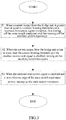
- FIG. 3 is a flowchart of a first embodiment, not falling under the scope of the present invention, of a current limiting control method for a three-level inverter.
- the current limiting control method for the three-level inverter as shown in FIG. 3 is applicable to various types of three-level inverters, such as I-type three-level inverters and T-type three-level inverters, a single-phase or multi-phase three-level inverters.
- the three-level inverter at least comprises a bridge arm including main switch transistors and auxiliary switch transistors.
- the current limiting control method for a three-level inverter according to the present invention comprises the following steps.
- step S1 when a current output from the bridge arm is greater than or equal to a current limiting threshold and a received overcurrent signal is enabled, first turning off the main switch transistors and then turning off the auxiliary switch transistors; step S2 of, when the current output from the bridge arm drops to lower than the current limiting threshold and the received overcurrent signal is disabled, turning on the auxiliary switch transistors.
- step S3 when the received overcurrent signal is disabled and a next PWM effective edge of the main switch transistors arrives, turning on the main switch transistors.
- FIG. 1 is a bridge arm output circuit diagram of an I-type three-level inverter.
- FIG. 6 is a normal current channel when the bridge arm output circuit in FIG. 1 operates with a resistive load in a positive half cycle of an output voltage.
- FIG. 7 is a current channel when the bridge arm output circuit in FIG. 1 is under current limiting control.
- the principle of the first embodiment of the current limiting control method for the three-level inverter as shown in FIG. 3 will be described as follows in combination with FIGS. 1 and 6-7 .
- the four switch transistors Q1-Q4 are in the following operating states: the auxiliary switch transistor Q2 is normally on, the main switch transistor Q4 is normally off, and the main switch transistor Q1 and the auxiliary switch transistor Q3 are complementarily turned on. It is further assumed that the current is in a direction of flowing from a bus to a load, and it is defined that the flow direction of the current is positive, that is, as shown in FIG. 1 , the flow direction of the inductive current I is positive.
- the inductive current I rises, an inductor L stores energy, at this time the voltage of the bridge arm output point A is a positive bus output voltage, and at this time the current loop is as shown by the real line in FIG. 6 .
- the main switch transistor Q1 is turned off and the auxiliary switch transistor Q3 is turned on, the inductive current I freewheels via the auxiliary switch transistor Q2, the voltage of the bridge arm output point A is at an N-point level, i.e., 0, and at this time the current loop is as shown by the dashed line in FIG. 6
- the inductive current I exceeds the set current limiting protection threshold, then current limiting logic is entered, the main switch transistor Q1 and the main switch transistor Q4 will be first turned off, and then the auxiliary switch transistor Q2 and the auxiliary switch transistor Q3 will be turned off after the main switch transistor Q1 is reliably turned off. After the auxiliary switch transistor Q2 and the auxiliary switch transistor Q3 are also completely turned off, the inductive current I will freewheels via a negative bus and freewheeling diodes D4, D3, the negative bus is charged, and the voltage of the bridge arm output point A is a negative bus output voltage. At this time the current loop is as shown in FIG. 7 .
- the inductive current I is surely dropping.
- the auxiliary switch transistors Q2 and Q3 are turned on first, and then the main switch transistors Q1 and Q4 are turned on, thus exiting the current limiting logic.
- the current limiting control method for a three-level inverter as shown in FIG. 3 of the present invention is proposed.
- step S1 of the present embodiment it is assumed that at a time t1 the inductive current I exceeds the set current-limiting current threshold, the overcurrent signal OCP is enabled, resulting in entering current limiting protection logic, the main transistors Q1 and Q4 are turned off such that the inductive current I no longer rises, and then the auxiliary switch transistors Q2 and Q3 are turned off, so as to complete transistor blockage logic.
- step S2 when the inductive current I drops to lower than the current limiting threshold, the overcurrent signal OCP is disabled, and at this time the auxiliary switch transistors Q2 and Q3 are directly turned on, without needing to wait for a PWM effective edge.
- the auxiliary switch transistors Q2 and Q3 are turned on, the inductive current I freewheels via the auxiliary switch transistors Q2 and Q3 and a neutral-point clamping diode, without irrigating a unilateral bus; in addition, at this time, the bridge arm output voltage is at a N-point level, i.e., 0, which is higher than the level of the negative bus when all the four switch transistors Q1-Q4 are blocked, the inductive voltage drops slightly and falls slightly, and the output voltage waveforms are also much better.
- step S3 when the received overcurrent signal is disabled and a next PWM effective edge of the main switch transistor Q1 and Q4 arrives, the main switch transistors Q1 and Q4 are turned on.
- the main switch transistors Q1 and Q4 still need to wait for a PWM effective edge, because if the main switch transistors Q1 and Q4 are turned on at this time, the inductive current I will again be caused to rise to exceed the current limiting threshold, thereby triggering another current limiting logic and thus increasing switching loss of devices.
- the auxiliary switch transistors are directly turned on, making it possible to ensure voltage waveform quality, and when a next PWM effective edge of the main switch transistors arrives, the main switch transistors are turned on, making it possible to ensure that a switching frequency of the switch transistors will not excessively increase, so as to reduce switching loss.
- FIG. 4 is a flowchart of a second embodiment of the current limiting control method for a three-level inverter according to the present invention.
- the current limiting control method for a three-level inverter as shown in FIG. 4 is applicable to various types of three-level inverters, such as I-type three-level inverters and T-type three-level inverters, single-phase or multi-phase three-level inverters.
- the three-level inverter at least comprises a bridge arm including main switch transistors and auxiliary switch transistors.
- the current limiting control method for a three-level inverter according to the present invention comprises the following steps.
- step S1 when a current output from the bridge arm is greater than or equal to a current limiting threshold and a received overcurrent signal is enabled, first turning off the main switch transistors and then turning off the auxiliary switch transistors.
- step S2 when the current output from the bridge arm drops to lower than the current limiting threshold and the received overcurrent signal is disabled, turning on the auxiliary switch transistors after elapse of a first delay time.
- step S3 when the current output from the bridge arms rises to greater than or equal to the current limiting threshold and the received overcurrent signal is enabled, again turning off the auxiliary switch transistors and no longer turning on the auxiliary switch transistors within this switching cycle.
- step S4 when the received overcurrent signal is disabled and a next PWM effective edge of the main switch transistors arrives, turning on the main switch transistors.
- the current limiting control method for a three-level inverter of the present embodiment will be described as follows also by taking the bridge arm output circuit of the I-type three-level inverter as shown in FIG. 1 as an example.
- the overcurrent signal OCP is enabled, resulting in entering current limiting protection logic, the main transistors Q1 and Q4 are turned off such that the inductive current I no longer rises, and then the auxiliary switch transistors Q2 and Q3 are turned off, so as to complete transistor blockage logic.
- step S2 when the inductive current I drops to lower than the current limiting threshold, the overcurrent signal OCP is disabled, and at this time the auxiliary switch transistors Q2 and Q3 are directly turned on, without needing to wait for a PWM effective edge.
- Such processing is under the assumption that when the auxiliary switch transistors Q2 and Q3 are turned on, the inductive current freewheels and will not rise.
- the output filter capacitive level is lower than the N-point level, i.e., 0 (for example when the bypass of a UPS is short-circuited or there are other active machines at the inverter output), or when the voltage and the current are of different polarities (for example II/IV quadrants of an inductive load and a capacitive load), in these operating conditions the inductive current will rise when the auxiliary switch transistors Q2 and Q3 are turned on. Then when the inductive current I again rises to higher than the current limiting threshold, the auxiliary switch transistors Q2 and Q3 are turned off.
- the above operating conditions are possibly repeated multiple times, causing switching of the auxiliary switch transistors Q2 and Q3 to be performed multiple times, resulting in that the loss abruptly increases.
- step S2 when the inductive current I drops to lower than the current limiting threshold, the overcurrent signal OCP is disabled, and the auxiliary switch transistors Q2 and Q3 are turned on after elapse of a first delay time (for example 2uS).
- a first delay time for example 2uS
- the diodes of the main switch transistors Q1 and Q4 freewheels.
- the first delay time is adjustable, and adjusting the first time delay can adjust the heat generation distribution between the diodes of the main switch transistors Q1 and Q4 and the diodes of the auxiliary switch transistors Q2 and Q3.
- step S3 since the auxiliary switch transistors Q2 and Q3 have been turned on, the inductive current I possibly again rises to equal to or greater than the current limiting threshold, resulting in that the overcurrent signal OCP is again disabled; at this time the auxiliary switch transistors Q2 and Q3 are turned off, then within this switching cycle, no matter whether the inductive current I drops to lower than the current limiting threshold, the auxiliary switch transistors Q2 and Q3 are no longer turned on. In this way, within one switching cycle, switching of the auxiliary switch transistors Q2 and Q3 is possibly performed once or twice. In the worst situation, the auxiliary switch transistors Q2 and Q3 are equivalent to being two-times multiplied. With respect to a normal operating condition, the switching loss is increased by one time. Thus, it is made possible to more efficiently control the switching frequency of the auxiliary switch transistors, so as to further reduce switching loss.
- step S3 when the received overcurrent signal is disabled and a next PWM effective edge of the main switch transistor Q1 and Q4 arrives, the main switch transistors Q1 and Q4 are turned on.
- the main switch transistors Q1 and Q4 still need to wait for a PWM effective edge, because if the main switch transistors Q1 and Q4 are turned on at this time, the inductive current I will again be caused to rise to exceed the current limiting threshold, thereby triggering another current limiting logic and thus increasing switching loss of devices.
- the auxiliary switch transistors are directly turned on, making it possible to ensure voltage waveform quality, and when a next PWM effective edge of the main switch transistors arrives, the main switch transistors are turned on, making it possible to ensure that a switching frequency of the switch transistors will not excessively increase, so as to reduce switching loss. Further, by limiting a switching frequency of the auxiliary switch transistors within each switching cycle, it is made possible to more efficiently control the switching frequency of the auxiliary switch transistors, so as to further reduce switching loss.
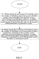
- FIG. 5 is a flowchart of a switching-frequency switching steps of auxiliary switch transistors of a third embodiment of the current limiting control method for a three-level inverter according to the present invention.
- the embodiment as shown in FIG. 4 may be further optimized to switch, based on the number of switching cycles during each of which current limit switching of the auxiliary switch transistors Q2 and Q3 has occurred twice, a switching frequency of the auxiliary switch transistors Q2 and Q3 within each switching cycle, so as to limit the switching frequency of the auxiliary switch transistors Q2 and Q3.
- step S1 when among the set number of switching cycles the number of switching cycles during each of which current limit switching of the auxiliary switch transistors has occurred twice is equal to or greater than a switching threshold, it is limited that current limit switching can be performed only once for the auxiliary switch transistors in consecutive cycles.
- step S2 when among the set number of switching cycles the number of switching cycles during each of which current limit switching of the auxiliary switch transistors has occurred once is equal to or greater than a switching threshold, it is allowed that current limit switching is performed twice for the auxiliary switch transistors in consecutive cycles.
- the number of switching cycles during each of which current limit switching of the auxiliary switch transistors Q2 and Q3 is performed once may be counted within the plurality of PWM switching cycles.
- the number is greater than the switching threshold, it is limited that current limit switching can be performed twice for the auxiliary switch transistors Q2 and Q3 in consecutive cycles.
- the process of current limiting de-blocking is as follows: when the inductive current I drops to below the current limiting threshold, the auxiliary switch transistors Q2 and A3 may be turned on according to logic, without needing to wait for arrival of a PWM effective edge of a next switching cycle. After the auxiliary switch transistors Q2 and A3 are turned on, the bridge arm side voltage is at 0 level, and since the load side voltage is 0 (the case of short circuit) or is positive (the case of rectifier load), the inductive current I will maintain unchanged or decreased, making it impossible to again enter current limiting. With respect to wave-by-wave current limiting, the auxiliary switch transistors Q2 and A3 are turned on in advance, thus ensuring voltage waveforms, and the number of times of switching does not change.
- the process of current limiting de-blocking is as follows: after the inductive current I drops to below the current limiting threshold, the auxiliary switch transistors Q2 and A3 are turned on according to logic; after the auxiliary switch transistors Q2 and A3 are turned on, the bridge arm side voltage is at 0 level, the load side is a bypass voltage source, the inductive current I possibly continues to increase, again triggering a current limiting point, the auxiliary switch transistors Q2 and A3 are turned off for a second time and no longer turned on, until an effective edge of a second switching cycle arrives. In the second switching cycle, the above operations are repeated.
- the current limiting mode is switched to wave-by-wave current limiting (current limit switching can be performed only once within the switching period). After consecutive 40 cycles of wave-by-wave current limiting, the current limiting mode is switched back to allow current limiting to be performed twice. The number of times of switching is increased by 5%, and the increase proportion of switching loss is small.
- the auxiliary switch transistors are directly turned on, making it possible to ensure voltage waveform quality, and when a next PWM effective edge of the main switch transistors arrives, the main switch transistors are turned on, making it possible to ensure that a switching frequency of the switch transistors will not excessively increase, so as to reduce switching loss. Further, by limiting a switching frequency of the auxiliary switch transistors within each switching cycle and controlling the number of times of two-time current limit switching of the auxiliary switch transistors within a plurality of cycles, it is made possible to more efficiently control the switching frequency of the auxiliary switch transistors, so as to further reduce switching loss.
- FIG. 8 is a principle block diagram of a first embodiment, not falling under the scope of the present invention, of a current limiting control device for a three-level inverter.
- the current limiting control device for a three-level inverter as shown in FIG. 8 is applicable to various types of three-level inverters, such as I-type three-level inverters and T-type three-level inverters, a single-phase or multi-phase three-level inverters.
- the three-level inverter at least comprises a bridge arm including main switch transistors and auxiliary switch transistors.
- the current limiting control device 800 comprises: a current limiting control module 810, an auxiliary switch transistor turn-on module 820 and a main switch transistor turn-on module 830.
- the current limiting control module 810 is used for, when a current output from the bridge arm is greater than or equal to a current limit threshold and a received overcurrent signal is enabled, first turning off the main switch transistors and then turning off the auxiliary switch transistors.
- the auxiliary switch transistor turn-on module 820 is used for, when the current output from the bridge arm drops to lower than the current limit threshold and the received overcurrent signal is disabled, turning on the auxiliary switch transistors.
- the main switch transistor turn-on module 830 is used for, when the received overcurrent signal is disabled and a next PWM effective edge of the main switch transistors arrives, turning on the main switch transistors.
- the current limiting control module 810, the auxiliary switch transistor turn-on module 820 and the main switch transistor turn-on module 830 may be constructed based on the current limiting control method for the three-level inverter as shown in FIG. 3 , which will not be repeatedly described herein.
- the auxiliary switch transistors are directly turned on, making it possible to ensure voltage waveform quality, and when a next PWM effective edge of the main switch transistors arrives, the main switch transistors are turned on, making it possible to ensure that a switching frequency of the switch transistors will not excessively increase, so as to reduce switching loss.
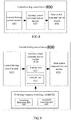
- FIG. 9 is a principle block diagram of a second embodiment of the current limiting control device for a three-level inverter according to the present invention.
- the current limiting control device for a three-level inverter as shown in FIG. 9 is applicable to various types of three-level inverters, such as I-type three-level inverters and T-type three-level inverters, a single-phase or multi-phase three-level inverters.
- the three-level inverter at least comprises a bridge arm including main switch transistors and auxiliary switch transistors.
- the current limiting control device 800 comprises: a current limiting control module 810, an auxiliary switch transistor turn-on module 820, a main switch transistor turn-on module 830 and a switching-frequency switching module 840.
- the current limiting control module 810 is used for, when a current output from the bridge arm is greater than or equal to a current limit threshold and a received overcurrent signal is enabled, first turning off the main switch transistors and then turning off the auxiliary switch transistors.
- the auxiliary switch transistor turn-on module 820 is used for, when the current output from the bridge arm drops to lower than the current limit threshold and the received overcurrent signal is disabled, turning on the auxiliary switch transistors.
- the main switch transistor turn-on module 830 is used for, when the received overcurrent signal is disabled and a next PWM effective edge of the main switch transistors arrives, turning on the main switch transistors.
- the switching-frequency switching module 840 is used for switching, based on the number of switching cycles during each of which current limit switching of the auxiliary switch transistors has occurred twice, a switching frequency of the auxiliary switch transistors within each switching cycle.
- the auxiliary switch transistor turn-on module 820 further comprises: a turn-on unit 821 and a turn-off unit 822.
- the turn-on unit 821 is used for, when the current output from the bridge arm drops to lower than the current limit threshold and the received overcurrent signal is disabled, turning on the auxiliary switch transistors after elapse of a first delay time.
- the turn-offunit 822 is used for, when the current output from the bridge arms rises to greater than or equal to the current limit threshold and the received overcurrent signal is enabled, again turning off the auxiliary switch transistors and no longer turning on the auxiliary switch transistors within this switching cycle.
- the switching-frequency switching module 840 further comprises: a switching limitation unit 841 and a switching transition unit 842.
- the switching limitation unit 841 is used for, when among the set number of switching cycles the number of switching cycles during each of which current limit switching of the auxiliary switch transistors has occurred twice is equal to or greater than a switching threshold, limiting the auxiliary switch transistors to be capable of performing current limit switching only once in consecutive cycles.
- the switching transition unit 842 is used for, when among the set number of switching cycles the number of switching cycles during each of which current limit switching of the auxiliary switch transistors has occurred once is equal to or greater than a switching threshold, allowing that current limit switching is performed twice for the auxiliary switch transistors in consecutive cycles.
- the current limiting control module 810, the auxiliary switch transistor turn-on module 820, the main switch transistor turn-on module 830 and the switching-frequency switching module 840, the turn-on unit 821 and the turn-off unit 822, as well as the switching limitation unit 841 and the switching transition unit 842 according to the present invention may be constructed based on the current limiting control methods of the three-level inverter as shown in FIGS. 4-5 , which will not be repeatedly described herein.
- the auxiliary switch transistors are directly turned on, making it possible to ensure voltage waveform quality, and when a next PWM effective edge of the main switch transistors arrives, the main switch transistors are turned on, making it possible to ensure that a switching frequency of the switch transistors will not excessively increase, so as to reduce switching loss.
- auxiliary switch transistors by limiting a switching frequency of the auxiliary switch transistors within each switching cycle and controlling the number of times of two-times current limit switching of the auxiliary switch transistors within a plurality of cycles, it is made possible to more efficiently control the switching frequency of the auxiliary switch transistors, so as to further reduce switching loss.
- the various devices, modules or units in the embodiments of the present invention may be integrated in one device, module or unit, and may also be separate physical existence individuals, and it is also possible that two or more devices, modules or units are integrated in one device, module or unit.
- the foregoing integrated devices, modules or units may be realized either in the form of hardware or in the form of software functional modules. If the integrated devices, modules or units are realized in the form of software functional modules and are sold or used as independent products, they may also be stored in a computer readable storage medium.
- the aforementioned storage medium may be an RAM, a magnetic disk or an optical disk or the like.
- the foregoing devices, apparatuses or systems may implement the methods in the corresponding method embodiments.
Landscapes
- Engineering & Computer Science (AREA)
- Power Engineering (AREA)
- Inverter Devices (AREA)
Description
- The present application claims the priority to
Chinese Patent Application No. 201711248722.9 - The present invention relates to a field of uninterruptible power supplies, and more particularly to a current limiting control method and device for a three-level inverter.
- A current limiting technique is a very important protection technique of an inverter, which can effectively protect power switch elements when the inverter suddenly is heavily loaded or has a short-circuited output, so as to improve the impact resistance of the inverter.
FIG. 1 shows a bridge arm output circuit diagram of a typical I-type three-level inverter. As shown inFIG. 1 , the I-type three-level inverter comprises four switch transistors, i.e., a main switch transistor Q1 and an auxiliary switch transistor Q2 which are located at an upper bridge arm, and a main switch transistor Q4 and an auxiliary switch transistor Q3 which are located at a lower bridge arm. - At the time of a current limiting blockage, first, the main switch transistors Q1 and Q4 shall be turned off, and then the auxiliary switch transistors Q2 and Q3 shall be blocked after the main switch transistors Q1 and Q4 are reliably blocked. When an inductive current I drops to below a current protection threshold, a current limiting signal disappears, and after the current limiting signal disappears, an appropriate timing is selected to start de-blocking logic; that is, first, the two auxiliary switch transistors Q2 and Q3 are compulsorily turned on for a period of time, and after the auxiliary switch transistors Q2 and Q3 are reliably turned on such that a midpoint level is established, an auxiliary switch transistor (e.g. Q3) which is unnecessarily normally turned on is then turned off for a period of time and thereafter Q2 and Q3 are controlled to act according to normal switching logic, then the main switch transistors Q1 and Q4 are turned on, and the main switch transistors Q1 and Q4 are controlled to act according to normal switching logic, thereby ending the current limiting process and entering normal wave generation logic. The appropriate timing indicated herein refers to: when the current limiting signal disappears, whether the de-blocking logic is started immediately or the de-blocking logic is not started until an effective edge of PWM arrives. Generally speaking, wave-by-wave current limiting refers to that after the current limiting signal disappears, the de-blocking logic is not started until an effective edge of PWM arrives. For MOSFETs or IGBTs with an enough switching speed, it is also possible to enter the de-blocking logic once it is confirmed that the current limiting signal disappears, without waiting for an effective edge of PWM, and this current limiting manner is referred to as non-wave-by-wave current limiting manner.
- However, in the existing current limiting techniques, the wave-by-wave current limiting manner has defects in regard to poor output voltage waveforms and in regard to mutual irrigation of energy between positive and negative buses; and although the non-wave-by-wave current limiting manner has better output voltage waveforms, it possibly involves more severe mutual irrigation of energy between positive and negative buses, resulting in a big risk of occurrence of an overvoltage to a unilateral bus, thus increasing a risk of damaging switch transistors.
- To remove the defects in the aforementioned technical solutions, there is proposed an improved solution: the wave-by-wave current limiting manner is adopted for the main switch transistors, and the non-wave-by-wave current limiting manner allowing multiple times of turn-ons within one PWM cycle is adopted for the auxiliary switch transistors, so as to turn on the auxiliary switch transistors once the current limiting signal disappears, letting a bridge arm output voltage be at an N-line level. However, this solution still has the following significant disadvantage: after occurrence of the wave-by-wave current limiting, switching of the auxiliary switch transistors is possibly performed multiple times within one switching cycle, which is equivalent to that a switching frequency of the auxiliary switch transistors is n-times multiplied, which will greatly increase switching loss of diodes of the auxiliary switch transistors and the main switch transistors.
-
EP 2 750 272 A1 -
CN 104 518 697 B discloses a current limit control method and a current limit control device of a three-level inverter. - The technical problem to be solved by the present invention lies in: providing, with respect to the above defects of the prior art, a current limiting control method and device for a three-level inverter which not only can ensure voltage waveform quality after occurrence of current limiting but also can ensure a switching frequency of switch transistors not to excessively increase.
- The technical solution adopted by the present invention to solve its technical problem is defined by a method according to claim 1 and a control device according to claim 4. Advantageous aspects of the invention are defined in the dependent claims.
- By implementing the current limiting control method and device for the three-level inverter according to the present invention, when the current output from the bridge arm drops to lower than the current limiting threshold, the auxiliary switch transistors are directly turned on, making it possible to ensure voltage waveform quality, and when a next PWM effective edge of the main switch transistors arrives, the main switch transistors are turned on, making it possible to ensure that a switching frequency of the switch transistors will not excessively increase, so as to reduce switching loss. Further, by limiting a switching frequency of the auxiliary switch transistors within each switching cycle and controlling the number of times of two-time current limit switching of the auxiliary switch transistors within a plurality of cycles, it is made possible to more efficiently control the switching frequency of the auxiliary switch transistors, so as to further reduce switching loss.
- Hereinafter, the present invention will be further described in combination with drawings and embodiments. In the drawings:
-
FIG. 1 is a bridge arm output circuit diagram of an I-type three-level inverter; -
FIG. 2 is a structural schematic diagram of a current limiting control system of an existing three-level inverter; -
FIG. 3 is a flowchart of a first embodiment not falling under the scope of the present invention of a current limiting control method for a three-level inverter; -
FIG. 4 is a flowchart of a second embodiment of the current limiting control method for a three-level inverter according to the present invention; -
FIG. 5 is a flowchart of a switching-frequency switching steps of auxiliary switch transistors of a third embodiment of the current limiting control method for a three-level inverter according to the present invention; -
FIG. 6 is a normal current channel when the bridge arm output circuit inFIG. 1 operates with a resistive load in a positive half cycle of an output voltage; -
FIG. 7 is a current channel when the bridge arm output circuit inFIG. 1 is under current limiting control; -
FIG. 8 is a principle block diagram of a first embodiment not falling under the scope of the present invention of a current limiting control device for a three-level inverter; -
FIG. 9 is a principle block diagram of a second embodiment of the current limiting control device for a three-level inverter according to the present invention. - To make the object, the technical solution and the advantage of the present invention more clear and explicit, the present invention will be further described in detail in combination with drawings and embodiments below. It should be understood that the specific embodiments described herein are used only to construe the present invention, but not to limit the present invention. The further explanations and descriptions of the present invention which are made below in combination with the drawings and the embodiments take the case of having a resistive load as an example.
- Referring to
FIG. 1 , a three-level inverter at least comprises a bridge arm including four switch transistors sequentially connected in series, wherein the four switch transistors are a main switch transistor Q1 and an auxiliary switch transistor Q2 which are located at an upper bridge arm, and a main switch transistor Q4 and an auxiliary switch transistor Q3 which are located at a lower bridge arm, respectively. Referring toFIG. 2 , in a current limiting control system of the three-level inverter, a wave generation control unit is used for outputting a direction signal (Dir) indicating that a current voltage is in a positive half cycle or a negative half cycle, and two branches of complementary PWM signals with dead zones, i.e., a PWM signal PWM1 of the main switch transistors and a PWM signal PWM2 of the auxiliary switch transistors, to a PWM control unit. The PWM control unit generates, according to the direction signal Dir and the two branches of complementary PWM signals with dead zones, four branches of PWM signals PWM_Q1, PWM_Q2, PWM_Q3 and PWM_Q4 which change according to predetermined logic, and respectively outputs the four branches of PWM signals to the four switch transistors Q1, Q2, Q3, Q4 in one phase of the three-level inverter, so as to drive the four switch transistors to act according to switching logic. A current detection unit is used for detecting an inductive current I, namely a current output from the bridge arm, i.e., a current flowing through the switch transistors, and converting the current I flowing through the switch transistors to a voltage and thereafter outputting it to an overcurrent judgment unit. The overcurrent judgment unit compares the received voltage value with a current-limiting voltage threshold (corresponding to a current-limiting current threshold), wherein if the received voltage value is greater than or equal to the current-limiting voltage threshold, an overcurrent signal output from the PWM control unit is enabled (the overcurrent signal output from the PWM control unit is changed from a low level to a high level), and if the received voltage value is less than the current-limiting voltage threshold, the overcurrent signal output from the PWM control unit is disabled (a low level is output). The PWM control unit judges, according to whether the received overcurrent signal is enabled, whether to perform current limiting control. -
FIG. 3 is a flowchart of a first embodiment, not falling under the scope of the present invention, of a current limiting control method for a three-level inverter. The current limiting control method for the three-level inverter as shown inFIG. 3 is applicable to various types of three-level inverters, such as I-type three-level inverters and T-type three-level inverters, a single-phase or multi-phase three-level inverters. The three-level inverter at least comprises a bridge arm including main switch transistors and auxiliary switch transistors. As shown inFIG. 3 , the current limiting control method for a three-level inverter according to the present invention comprises the following steps. At step S1, when a current output from the bridge arm is greater than or equal to a current limiting threshold and a received overcurrent signal is enabled, first turning off the main switch transistors and then turning off the auxiliary switch transistors; step S2 of, when the current output from the bridge arm drops to lower than the current limiting threshold and the received overcurrent signal is disabled, turning on the auxiliary switch transistors. At step S3, when the received overcurrent signal is disabled and a next PWM effective edge of the main switch transistors arrives, turning on the main switch transistors. -
FIG. 1 is a bridge arm output circuit diagram of an I-type three-level inverter.FIG. 6 is a normal current channel when the bridge arm output circuit inFIG. 1 operates with a resistive load in a positive half cycle of an output voltage.FIG. 7 is a current channel when the bridge arm output circuit inFIG. 1 is under current limiting control. Hereinafter, the principle of the first embodiment of the current limiting control method for the three-level inverter as shown inFIG. 3 will be described as follows in combination withFIGS. 1 and6-7 . - If the current circuit operates in the positive half cycle of the output voltage, the four switch transistors Q1-Q4 are in the following operating states: the auxiliary switch transistor Q2 is normally on, the main switch transistor Q4 is normally off, and the main switch transistor Q1 and the auxiliary switch transistor Q3 are complementarily turned on. It is further assumed that the current is in a direction of flowing from a bus to a load, and it is defined that the flow direction of the current is positive, that is, as shown in
FIG. 1 , the flow direction of the inductive current I is positive. - When the main switch transistor Q1 is turned on and the auxiliary switch transistor Q3 is turned off, the inductive current I rises, an inductor L stores energy, at this time the voltage of the bridge arm output point A is a positive bus output voltage, and at this time the current loop is as shown by the real line in
FIG. 6 . When the main switch transistor Q1 is turned off and the auxiliary switch transistor Q3 is turned on, the inductive current I freewheels via the auxiliary switch transistor Q2, the voltage of the bridge arm output point A is at an N-point level, i.e., 0, and at this time the current loop is as shown by the dashed line inFIG. 6 - If the inductive current I exceeds the set current limiting protection threshold, then current limiting logic is entered, the main switch transistor Q1 and the main switch transistor Q4 will be first turned off, and then the auxiliary switch transistor Q2 and the auxiliary switch transistor Q3 will be turned off after the main switch transistor Q1 is reliably turned off. After the auxiliary switch transistor Q2 and the auxiliary switch transistor Q3 are also completely turned off, the inductive current I will freewheels via a negative bus and freewheeling diodes D4, D3, the negative bus is charged, and the voltage of the bridge arm output point A is a negative bus output voltage. At this time the current loop is as shown in
FIG. 7 . - When all the four switch transistors Q1-Q4 are off, the inductive current I is surely dropping. After the inductive current I drops to below the current limiting threshold, the auxiliary switch transistors Q2 and Q3 are turned on first, and then the main switch transistors Q1 and Q4 are turned on, thus exiting the current limiting logic.
- After the inductive current I is lower than the current limiting protection threshold, entry into de-blocking logic may be considered. For wave-by-wave current limiting, it is necessary to wait for a PWM effective edge. If the PWM effective edge does not arrive, blocking of the four switch transistors continues. This will cause the inductive current to drastically drop. The worst situation is that when the PWM effective edge arrives, the inductive current has not been lower than the current limiting protection threshold or completion of de-blocking logic has not been confirmed although the inductive current has been lower than the threshold, and this will cause all the four switch transistors to be turned off within a next PWM cycle. In this case, the inductive current even will fall from a peak value to near zero, resulting in that output voltage waveforms are very poor at the time of the wave-by-wave current limiting. For non-wave-by-wave current limiting, such a problem does not exist. However, if de-blocking logic is completed, when the inductive current again exceeds the current limiting threshold because the main switch transistor Q1 continues to be on, it is again necessary to enter current-limiting wave blockage logic. Such repeated steps will cause multiple times of wave blockage within a next PWM cycle.
- Thus, the current limiting control method for a three-level inverter as shown in
FIG. 3 of the present invention is proposed. At step S1 of the present embodiment, it is assumed that at a time t1 the inductive current I exceeds the set current-limiting current threshold, the overcurrent signal OCP is enabled, resulting in entering current limiting protection logic, the main transistors Q1 and Q4 are turned off such that the inductive current I no longer rises, and then the auxiliary switch transistors Q2 and Q3 are turned off, so as to complete transistor blockage logic. - At step S2, when the inductive current I drops to lower than the current limiting threshold, the overcurrent signal OCP is disabled, and at this time the auxiliary switch transistors Q2 and Q3 are directly turned on, without needing to wait for a PWM effective edge. The benefit of such doing is: after the auxiliary switch transistors Q2 and Q3 are turned on, the inductive current I freewheels via the auxiliary switch transistors Q2 and Q3 and a neutral-point clamping diode, without irrigating a unilateral bus; in addition, at this time, the bridge arm output voltage is at a N-point level, i.e., 0, which is higher than the level of the negative bus when all the four switch transistors Q1-Q4 are blocked, the inductive voltage drops slightly and falls slightly, and the output voltage waveforms are also much better.
- At step S3, when the received overcurrent signal is disabled and a next PWM effective edge of the main switch transistor Q1 and Q4 arrives, the main switch transistors Q1 and Q4 are turned on. At this step, the main switch transistors Q1 and Q4 still need to wait for a PWM effective edge, because if the main switch transistors Q1 and Q4 are turned on at this time, the inductive current I will again be caused to rise to exceed the current limiting threshold, thereby triggering another current limiting logic and thus increasing switching loss of devices. Thus at this time, it is unnecessary to immediately turn on the main switch transistors Q1 and Q4, and it is more appropriate to wait for a next PWM effective edge.
- By implementing the current limiting control method for the three-level inverter according to the present invention, when the current output from the bridge arm drops to lower than the current limiting threshold, the auxiliary switch transistors are directly turned on, making it possible to ensure voltage waveform quality, and when a next PWM effective edge of the main switch transistors arrives, the main switch transistors are turned on, making it possible to ensure that a switching frequency of the switch transistors will not excessively increase, so as to reduce switching loss.
-
FIG. 4 is a flowchart of a second embodiment of the current limiting control method for a three-level inverter according to the present invention. The current limiting control method for a three-level inverter as shown inFIG. 4 is applicable to various types of three-level inverters, such as I-type three-level inverters and T-type three-level inverters, single-phase or multi-phase three-level inverters. The three-level inverter at least comprises a bridge arm including main switch transistors and auxiliary switch transistors. As shown inFIG. 4 , the current limiting control method for a three-level inverter according to the present invention comprises the following steps. At step S1, when a current output from the bridge arm is greater than or equal to a current limiting threshold and a received overcurrent signal is enabled, first turning off the main switch transistors and then turning off the auxiliary switch transistors. At step S2, when the current output from the bridge arm drops to lower than the current limiting threshold and the received overcurrent signal is disabled, turning on the auxiliary switch transistors after elapse of a first delay time. At step S3, when the current output from the bridge arms rises to greater than or equal to the current limiting threshold and the received overcurrent signal is enabled, again turning off the auxiliary switch transistors and no longer turning on the auxiliary switch transistors within this switching cycle. At step S4, when the received overcurrent signal is disabled and a next PWM effective edge of the main switch transistors arrives, turning on the main switch transistors. - Hereinafter, the current limiting control method for a three-level inverter of the present embodiment will be described as follows also by taking the bridge arm output circuit of the I-type three-level inverter as shown in
FIG. 1 as an example. At step S1 of the present embodiment, it is assumed that at a time t1 the inductive current I exceeds the set current-limiting current threshold, the overcurrent signal OCP is enabled, resulting in entering current limiting protection logic, the main transistors Q1 and Q4 are turned off such that the inductive current I no longer rises, and then the auxiliary switch transistors Q2 and Q3 are turned off, so as to complete transistor blockage logic. - In the embodiment as shown in
FIG. 3 , at step S2, when the inductive current I drops to lower than the current limiting threshold, the overcurrent signal OCP is disabled, and at this time the auxiliary switch transistors Q2 and Q3 are directly turned on, without needing to wait for a PWM effective edge. Such processing is under the assumption that when the auxiliary switch transistors Q2 and Q3 are turned on, the inductive current freewheels and will not rise. However, in the case of actual loading, it is also possible that when the output filter capacitive level is lower than the N-point level, i.e., 0 (for example when the bypass of a UPS is short-circuited or there are other active machines at the inverter output), or when the voltage and the current are of different polarities (for example II/IV quadrants of an inductive load and a capacitive load), in these operating conditions the inductive current will rise when the auxiliary switch transistors Q2 and Q3 are turned on. Then when the inductive current I again rises to higher than the current limiting threshold, the auxiliary switch transistors Q2 and Q3 are turned off. The above operating conditions are possibly repeated multiple times, causing switching of the auxiliary switch transistors Q2 and Q3 to be performed multiple times, resulting in that the loss abruptly increases. - With respect to such a deficiency, in the present embodiment, the following optimization steps are proposed. At step S2, when the inductive current I drops to lower than the current limiting threshold, the overcurrent signal OCP is disabled, and the auxiliary switch transistors Q2 and Q3 are turned on after elapse of a first delay time (for example 2uS). In the first delay time, the diodes of the main switch transistors Q1 and Q4 freewheels. The first delay time is adjustable, and adjusting the first time delay can adjust the heat generation distribution between the diodes of the main switch transistors Q1 and Q4 and the diodes of the auxiliary switch transistors Q2 and Q3. At step S3, since the auxiliary switch transistors Q2 and Q3 have been turned on, the inductive current I possibly again rises to equal to or greater than the current limiting threshold, resulting in that the overcurrent signal OCP is again disabled; at this time the auxiliary switch transistors Q2 and Q3 are turned off, then within this switching cycle, no matter whether the inductive current I drops to lower than the current limiting threshold, the auxiliary switch transistors Q2 and Q3 are no longer turned on. In this way, within one switching cycle, switching of the auxiliary switch transistors Q2 and Q3 is possibly performed once or twice. In the worst situation, the auxiliary switch transistors Q2 and Q3 are equivalent to being two-times multiplied. With respect to a normal operating condition, the switching loss is increased by one time. Thus, it is made possible to more efficiently control the switching frequency of the auxiliary switch transistors, so as to further reduce switching loss.
- At step S3, when the received overcurrent signal is disabled and a next PWM effective edge of the main switch transistor Q1 and Q4 arrives, the main switch transistors Q1 and Q4 are turned on. At this step, the main switch transistors Q1 and Q4 still need to wait for a PWM effective edge, because if the main switch transistors Q1 and Q4 are turned on at this time, the inductive current I will again be caused to rise to exceed the current limiting threshold, thereby triggering another current limiting logic and thus increasing switching loss of devices. Thus at this time, it is unnecessary to immediately turn on the main switch transistors Q1 and Q4, and it is more appropriate to wait for a next PWM effective edge.
- By implementing the current limiting control method for a three-level inverter according to the present invention, when the current output from the bridge arm drops to lower than the current limiting threshold, the auxiliary switch transistors are directly turned on, making it possible to ensure voltage waveform quality, and when a next PWM effective edge of the main switch transistors arrives, the main switch transistors are turned on, making it possible to ensure that a switching frequency of the switch transistors will not excessively increase, so as to reduce switching loss. Further, by limiting a switching frequency of the auxiliary switch transistors within each switching cycle, it is made possible to more efficiently control the switching frequency of the auxiliary switch transistors, so as to further reduce switching loss.
-
FIG. 5 is a flowchart of a switching-frequency switching steps of auxiliary switch transistors of a third embodiment of the current limiting control method for a three-level inverter according to the present invention. The embodiment as shown inFIG. 4 may be further optimized to switch, based on the number of switching cycles during each of which current limit switching of the auxiliary switch transistors Q2 and Q3 has occurred twice, a switching frequency of the auxiliary switch transistors Q2 and Q3 within each switching cycle, so as to limit the switching frequency of the auxiliary switch transistors Q2 and Q3. - As shown in
FIG. 5 , at step S1, when among the set number of switching cycles the number of switching cycles during each of which current limit switching of the auxiliary switch transistors has occurred twice is equal to or greater than a switching threshold, it is limited that current limit switching can be performed only once for the auxiliary switch transistors in consecutive cycles. At step S2, when among the set number of switching cycles the number of switching cycles during each of which current limit switching of the auxiliary switch transistors has occurred once is equal to or greater than a switching threshold, it is allowed that current limit switching is performed twice for the auxiliary switch transistors in consecutive cycles. - For example, the number of switching cycles during each of which current limit switching of the auxiliary switch transistors Q2 and Q3 is performed twice may be counted within a plurality of PWM switching cycles. When it is found that the number is greater than the switching threshold, it is limited that current limit switching can be performed only once for the auxiliary switch transistors Q2 and Q3 in consecutive cycles. For example, if within the plurality of cycles it is found that the case where current limit switching of the auxiliary switch transistors Q2 and Q3 is performed twice within one cycle has occurred during each of N1 (for example N1=2) switching cycles, it may be limited that within subsequent consecutive N2 (for example N2=40) cycles, current limit switching can be performed only once for the auxiliary switch transistors Q2 and Q3 within each switching cycle. Then, the number of switching cycles during each of which current limit switching of the auxiliary switch transistors Q2 and Q3 is performed once may be counted within the plurality of PWM switching cycles. When it is found that the number is greater than the switching threshold, it is limited that current limit switching can be performed twice for the auxiliary switch transistors Q2 and Q3 in consecutive cycles. Through such limitations, when current limiting is performed, the switching frequency of the auxiliary switch transistors Q2 and Q3 is at most increased to (1+N1/N2) times. For example: when N1=2 and N2=40, the frequency is increased by five percent.
- In current limiting protection such as short circuit, sudden rectifier load and the like in most of operating conditions, the process of current limiting de-blocking is as follows: when the inductive current I drops to below the current limiting threshold, the auxiliary switch transistors Q2 and A3 may be turned on according to logic, without needing to wait for arrival of a PWM effective edge of a next switching cycle. After the auxiliary switch transistors Q2 and A3 are turned on, the bridge arm side voltage is at 0 level, and since the load side voltage is 0 (the case of short circuit) or is positive (the case of rectifier load), the inductive current I will maintain unchanged or decreased, making it impossible to again enter current limiting. With respect to wave-by-wave current limiting, the auxiliary switch transistors Q2 and A3 are turned on in advance, thus ensuring voltage waveforms, and the number of times of switching does not change.
- During current limiting protection in extreme cases, such as common conduction of a main circuit and a bypass, the process of current limiting de-blocking is as follows: after the inductive current I drops to below the current limiting threshold, the auxiliary switch transistors Q2 and A3 are turned on according to logic; after the auxiliary switch transistors Q2 and A3 are turned on, the bridge arm side voltage is at 0 level, the load side is a bypass voltage source, the inductive current I possibly continues to increase, again triggering a current limiting point, the auxiliary switch transistors Q2 and A3 are turned off for a second time and no longer turned on, until an effective edge of a second switching cycle arrives. In the second switching cycle, the above operations are repeated. In the third switching period, the current limiting mode is switched to wave-by-wave current limiting (current limit switching can be performed only once within the switching period). After consecutive 40 cycles of wave-by-wave current limiting, the current limiting mode is switched back to allow current limiting to be performed twice. The number of times of switching is increased by 5%, and the increase proportion of switching loss is small.
- By implementing the current limiting control method for a three-level inverter according to the present invention, when the current output from the bridge arm drops to lower than the current limiting threshold, the auxiliary switch transistors are directly turned on, making it possible to ensure voltage waveform quality, and when a next PWM effective edge of the main switch transistors arrives, the main switch transistors are turned on, making it possible to ensure that a switching frequency of the switch transistors will not excessively increase, so as to reduce switching loss. Further, by limiting a switching frequency of the auxiliary switch transistors within each switching cycle and controlling the number of times of two-time current limit switching of the auxiliary switch transistors within a plurality of cycles, it is made possible to more efficiently control the switching frequency of the auxiliary switch transistors, so as to further reduce switching loss.
-
FIG. 8 is a principle block diagram of a first embodiment, not falling under the scope of the present invention, of a current limiting control device for a three-level inverter. The current limiting control device for a three-level inverter as shown inFIG. 8 is applicable to various types of three-level inverters, such as I-type three-level inverters and T-type three-level inverters, a single-phase or multi-phase three-level inverters. The three-level inverter at least comprises a bridge arm including main switch transistors and auxiliary switch transistors. - As shown in
FIG. 8 , the current limitingcontrol device 800 comprises: a current limitingcontrol module 810, an auxiliary switch transistor turn-onmodule 820 and a main switch transistor turn-onmodule 830. As shown inFIG. 8 , the current limitingcontrol module 810 is used for, when a current output from the bridge arm is greater than or equal to a current limit threshold and a received overcurrent signal is enabled, first turning off the main switch transistors and then turning off the auxiliary switch transistors. The auxiliary switch transistor turn-onmodule 820 is used for, when the current output from the bridge arm drops to lower than the current limit threshold and the received overcurrent signal is disabled, turning on the auxiliary switch transistors. The main switch transistor turn-onmodule 830 is used for, when the received overcurrent signal is disabled and a next PWM effective edge of the main switch transistors arrives, turning on the main switch transistors. - As appreciated by those skilled in the art, the current limiting
control module 810, the auxiliary switch transistor turn-onmodule 820 and the main switch transistor turn-onmodule 830 according to the present invention may be constructed based on the current limiting control method for the three-level inverter as shown inFIG. 3 , which will not be repeatedly described herein. - By implementing the current limiting control device for a three-level inverter according to the present invention, when the current output from the bridge arm drops to lower than the current limiting threshold, the auxiliary switch transistors are directly turned on, making it possible to ensure voltage waveform quality, and when a next PWM effective edge of the main switch transistors arrives, the main switch transistors are turned on, making it possible to ensure that a switching frequency of the switch transistors will not excessively increase, so as to reduce switching loss.
-
FIG. 9 is a principle block diagram of a second embodiment of the current limiting control device for a three-level inverter according to the present invention. The current limiting control device for a three-level inverter as shown inFIG. 9 is applicable to various types of three-level inverters, such as I-type three-level inverters and T-type three-level inverters, a single-phase or multi-phase three-level inverters. The three-level inverter at least comprises a bridge arm including main switch transistors and auxiliary switch transistors. - As shown in
FIG. 9 , the current limitingcontrol device 800 comprises: a current limitingcontrol module 810, an auxiliary switch transistor turn-onmodule 820, a main switch transistor turn-onmodule 830 and a switching-frequency switching module 840. As shown inFIG. 9 , the current limitingcontrol module 810 is used for, when a current output from the bridge arm is greater than or equal to a current limit threshold and a received overcurrent signal is enabled, first turning off the main switch transistors and then turning off the auxiliary switch transistors. The auxiliary switch transistor turn-onmodule 820 is used for, when the current output from the bridge arm drops to lower than the current limit threshold and the received overcurrent signal is disabled, turning on the auxiliary switch transistors. The main switch transistor turn-onmodule 830 is used for, when the received overcurrent signal is disabled and a next PWM effective edge of the main switch transistors arrives, turning on the main switch transistors. The switching-frequency switching module 840 is used for switching, based on the number of switching cycles during each of which current limit switching of the auxiliary switch transistors has occurred twice, a switching frequency of the auxiliary switch transistors within each switching cycle. - Further as shown in
FIG. 9 , the auxiliary switch transistor turn-onmodule 820 further comprises: a turn-onunit 821 and a turn-offunit 822. The turn-onunit 821 is used for, when the current output from the bridge arm drops to lower than the current limit threshold and the received overcurrent signal is disabled, turning on the auxiliary switch transistors after elapse of a first delay time. The turn-offunit 822 is used for, when the current output from the bridge arms rises to greater than or equal to the current limit threshold and the received overcurrent signal is enabled, again turning off the auxiliary switch transistors and no longer turning on the auxiliary switch transistors within this switching cycle. - The switching-frequency switching module 840 further comprises: a switching
limitation unit 841 and aswitching transition unit 842. The switchinglimitation unit 841 is used for, when among the set number of switching cycles the number of switching cycles during each of which current limit switching of the auxiliary switch transistors has occurred twice is equal to or greater than a switching threshold, limiting the auxiliary switch transistors to be capable of performing current limit switching only once in consecutive cycles. The switchingtransition unit 842 is used for, when among the set number of switching cycles the number of switching cycles during each of which current limit switching of the auxiliary switch transistors has occurred once is equal to or greater than a switching threshold, allowing that current limit switching is performed twice for the auxiliary switch transistors in consecutive cycles. - As appreciated by those skilled in the art, the current limiting
control module 810, the auxiliary switch transistor turn-onmodule 820, the main switch transistor turn-onmodule 830 and the switching-frequency switching module 840, the turn-onunit 821 and the turn-offunit 822, as well as the switchinglimitation unit 841 and theswitching transition unit 842 according to the present invention may be constructed based on the current limiting control methods of the three-level inverter as shown inFIGS. 4-5 , which will not be repeatedly described herein. - By implementing the current limiting control method for a three-level inverter according to the present invention, when the current output from the bridge arm drops to lower than the current limiting threshold, the auxiliary switch transistors are directly turned on, making it possible to ensure voltage waveform quality, and when a next PWM effective edge of the main switch transistors arrives, the main switch transistors are turned on, making it possible to ensure that a switching frequency of the switch transistors will not excessively increase, so as to reduce switching loss. Further, by limiting a switching frequency of the auxiliary switch transistors within each switching cycle and controlling the number of times of two-times current limit switching of the auxiliary switch transistors within a plurality of cycles, it is made possible to more efficiently control the switching frequency of the auxiliary switch transistors, so as to further reduce switching loss.
- The foregoing are only optimal embodiments of the present invention, but are not used to limit the present invention. Any modification, equivalent substitution and improvement and the like made within the scope of the present invention, as defined by the appended claims, should be contained in the scope of protection of the present invention. Moreover, although the present disclosure has been shown and described with respect to one or more implementations, those skilled in the art would conceive of equivalent variants and modifications based on the reading and understanding to the Description and the Drawings. The present disclosure includes all such modifications and variants, and is limited only by the scope of the appended claims. Particularly with regard to the various functions implemented by the above devices, modules or units, terms for describing such devices, modules or units aim to correspond to any device, module or unit that implements the specified functions of the devices, modules or units (for example they are equivalent in terms of functions) (unless otherwise indicated), even if they are not equivalent to the disclosed structures that implement the functions in the exemplary implementations of the present disclosure as shown herein. In addition, although the specified features of the present disclosure have been disclosed with respect to only one of several implementations, such features may be combined with for example one or more other features of other implementations which could be desired and advantageous for given or specific applications.
- The various devices, modules or units in the embodiments of the present invention may be integrated in one device, module or unit, and may also be separate physical existence individuals, and it is also possible that two or more devices, modules or units are integrated in one device, module or unit. The foregoing integrated devices, modules or units may be realized either in the form of hardware or in the form of software functional modules. If the integrated devices, modules or units are realized in the form of software functional modules and are sold or used as independent products, they may also be stored in a computer readable storage medium. The aforementioned storage medium may be an RAM, a magnetic disk or an optical disk or the like. The foregoing devices, apparatuses or systems may implement the methods in the corresponding method embodiments.
- The foregoing are only optimal embodiments of the present invention, but are not used to limit the present invention. Any modification, equivalent substitution and improvement and the like made within the scope of the present invention, as defined by the appended claims, should be contained in the scope of protection of the present invention.
Claims (6)
- A current limiting control method for a three-level inverter which comprises an I-type three-level inverter or a T-type three-level inverter, wherein the three-level inverter at least comprises a bridge arm including four switch transistors, the four switch transistors comprising main switch transistors (Q1, Q4) and auxiliary switch transistors (Q2, Q3), wherein each main switch transistor (Q1, Q4) is configured to connect an output of the three-level inverter to a positive bus or to a negative bus, and each auxiliary switch transistor (Q2, Q3) is configured to connect the output of the three-level inverter to a neutral point between the positive bus and the negative bus,
wherein the method comprises the following steps:S1. when a current output from the bridge arm is greater than or equal to a current limiting threshold and a received overcurrent signal is enabled, first turning off the main switch transistors (Q1, Q4) and then turning off the auxiliary switch transistors (Q2, Q3);S2. when the current output from the bridge arm drops to lower than the current limiting threshold and the received overcurrent signal is disabled, turning on the auxiliary switch transistors (Q2, Q3);S3. when the received overcurrent signal is disabled and a next PWM effective edge of the main switch transistors (Q1, Q4) arrives, turning on the main switch transistors (Q1, Q4),characterized in that the step S2 further comprises:S21. when the current output from the bridge arm drops to lower than the current limiting threshold and the received overcurrent signal is disabled, turning on the auxiliary switch transistors (Q2, Q3) after elapse of a first delay time;S22. when the current output from the bridge arms rises to greater than or equal to the current limiting threshold and the received overcurrent signal is enabled, again turning off the auxiliary switch transistors (Q2, Q3) and no longer turning on the auxiliary switch transistors (Q2, Q3) within this switching cycle. - The current limiting control method for a three-level inverter according to claim 1, characterized by further comprising:
S4. limiting, based on the number of switching cycles during which current limit switching of the auxiliary switch transistors (Q2, Q3) has occurred twice, a switching frequency of the auxiliary switch transistors (Q2, Q3) within each switching cycle. - The current limiting control method for a three-level inverter according to claim 2, characterized in that the step S4 further comprises:S41. when among a set number of switching cycles the number of switching cycles during which current limit switching of the auxiliary switch transistors (Q2, Q3) has occurred twice is equal to or greater than a switching threshold, limiting current limit switching to be performed only once for the auxiliary switch transistors (Q2, Q3) in consecutive cycles;S42. when among the set number of switching cycles the number of switching cycles during which current limit switching of the auxiliary switch transistors (Q2, Q3) has occurred once is equal to or greater than a switching threshold, allowing current limit switching to be performed twice for the auxiliary switch transistors (Q2, Q3) in consecutive cycles.
- A current limiting control device for a three-level inverter which comprises an I-type three-level inverter or a T-type three-level inverter, wherein the current limiting control device at least comprises a bridge arm including four switch transistors, the four switch transistors comprising main switch transistors (Q1, Q4) and auxiliary switch transistors (Q2, Q3), wherein each main switch transistor (Q1, Q4) is configured to connect an output of the three-level inverter to a positive bus or to a negative bus, and each auxiliary switch transistor (Q2, Q3) is configured to connect the output of the three-level inverter to a neutral point between the positive bus and the negative bus,
wherein the current limiting control device comprises:a current limiting control module (810) configured to, when a current output from the bridge arm is greater than or equal to a current limiting threshold and a received overcurrent signal is enabled, first turn off the main switch transistors (Q1, Q4) and then turn off the auxiliary switch transistors (Q2, Q3);an auxiliary switch transistor turn-on module (820) configured to, when the current output from the bridge arm drops to lower than the current limiting threshold and the received overcurrent signal is disabled, turn on the auxiliary switch transistors (Q2, Q3); a main switch transistor turn-on module (830) configured to, when the received overcurrent signal is disabled and a next PWM effective edge of the main switch transistors (Q1, Q4) arrives, turn on the main switch transistors (Q1, Q4), characterized in that the auxiliary switch transistor turn-on module (820) further comprises:a turn-on unit (821) configured to, when the current output from the bridge arm drops to lower than the current limiting threshold and the received overcurrent signal is disabled, turn on the auxiliary switch transistors (Q2, Q3) after elapse of a first delay time;a turn-off unit (822) configured to, when the current output from the bridge arms rises to greater than or equal to the current limiting threshold and the received overcurrent signal is enabled, again turn off the auxiliary switch transistors (Q2, Q3) and no longer turn on the auxiliary switch transistors (Q2, Q3) within this switching cycle. - The current limiting control device (800) for a three-level inverter according to claim 4, further comprising:
a switching-frequency switching module (840) configured to limit, based on the number of switching cycles during which current limit switching of the auxiliary switch transistors has occurred twice, a switching frequency of the auxiliary switch transistors (Q2, Q3) within each switching cycle. - The current limiting control device (800) for a three-level inverter according to claim 5, characterized in that the switching-frequency switching module (840) further comprises:a switching limitation unit (841) configured to, when among a set number of switching cycles the number of switching cycles during which current limit switching of the auxiliary switch transistors (Q2, Q3) has occurred twice is equal to or greater than a switching threshold, limit current limit switching to be performed only once for the auxiliary switch transistors (Q2, Q3) in consecutive cycles;a switching transition unit (842) configured to, when among the set number of switching cycles the number of switching cycles during which current limit switching of the auxiliary switch transistors (Q2, Q3) has occurred once is equal to or greater than a switching threshold, allow current limit switching to be performed twice for the auxiliary switch transistors (Q2, Q3) in consecutive cycles.
Applications Claiming Priority (1)
| Application Number | Priority Date | Filing Date | Title |
|---|---|---|---|
| CN201711248722.9A CN109873556B (en) | 2017-12-01 | 2017-12-01 | Current-limiting control method and device of three-level inverter |
Publications (2)
| Publication Number | Publication Date |
|---|---|
| EP3493381A1 EP3493381A1 (en) | 2019-06-05 |
| EP3493381B1 true EP3493381B1 (en) | 2021-07-07 |
Family
ID=62386102
Family Applications (1)
| Application Number | Title | Priority Date | Filing Date |
|---|---|---|---|
| EP18174276.8A Active EP3493381B1 (en) | 2017-12-01 | 2018-05-25 | Current limiting control method and device for three-level inverter |
Country Status (3)
| Country | Link |
|---|---|
| US (1) | US10594208B2 (en) |
| EP (1) | EP3493381B1 (en) |
| CN (1) | CN109873556B (en) |
Families Citing this family (15)
| Publication number | Priority date | Publication date | Assignee | Title |
|---|---|---|---|---|
| CN110460019B (en) * | 2019-09-11 | 2021-07-23 | 深圳市永联科技股份有限公司 | A control method and device for short-circuit protection of bridge converter |
| CN111262223B (en) * | 2020-03-19 | 2021-04-20 | 中国南方电网有限责任公司超高压输电公司柳州局 | Temporary locking protection configuration method and system for flexible direct-current series double valve groups |
| CN113114061B (en) * | 2021-03-26 | 2022-06-24 | 台达电子企业管理(上海)有限公司 | Converter and method for suppressing circulating current interference of converter |
| CN112959964B (en) * | 2021-03-27 | 2022-11-22 | 华为数字能源技术有限公司 | Power supply system of motor control module and vehicle |
| CN113659837B (en) * | 2021-07-05 | 2023-08-04 | 华为数字能源技术有限公司 | Converter, converter control method and power adapter |
| CN116015085A (en) * | 2021-10-21 | 2023-04-25 | 株洲变流技术国家工程研究中心有限公司 | Half-bridge control system and control method |
| CN114421796A (en) * | 2021-12-31 | 2022-04-29 | 深圳市禾望科技有限公司 | I-type three-level topological overcurrent sealing wave control method |
| CN114825998A (en) * | 2022-01-20 | 2022-07-29 | 西安星辰电气有限公司 | Output voltage reconstruction method of three-level inverter based on switching state |
| CN114447889B (en) * | 2022-04-11 | 2022-07-08 | 浙江日风电气股份有限公司 | Protection method, device and medium for grid-connected inverter |
| CN114825894B (en) * | 2022-06-22 | 2022-09-27 | 锦浪科技股份有限公司 | Wave-by-wave current limiting control method and device for Heric inverter circuit and inverter |
| CN115580201A (en) * | 2022-09-23 | 2023-01-06 | 华为数字能源技术有限公司 | Motor controller, power assembly and electric automobile |
| CN115498692A (en) * | 2022-10-13 | 2022-12-20 | 阳光电源股份有限公司 | New energy power generation system, wind power converter, photovoltaic inverter, voltage source AC-DC converter and its low-voltage ride-through method |
| CN116093894A (en) * | 2023-02-16 | 2023-05-09 | 青岛鼎信通讯科技有限公司 | Startup and shutdown protection method applied to I-shaped three-level topology |
| CN116111824B (en) * | 2023-03-06 | 2025-04-11 | 苏州贝瓦科技有限公司 | Control method and device for three-level circuit |
| CN117439396B (en) * | 2023-12-20 | 2024-04-16 | 杭州闪充聚能新能源有限公司 | Wave-by-wave current limiting protection system |
Citations (1)
| Publication number | Priority date | Publication date | Assignee | Title |
|---|---|---|---|---|
| US20120218785A1 (en) * | 2011-02-24 | 2012-08-30 | Jin Li | Three-Level Active Neutral Point Clamped Zero Voltage Switching Converter |
Family Cites Families (11)
| Publication number | Priority date | Publication date | Assignee | Title |
|---|---|---|---|---|
| JP5511976B2 (en) * | 2010-10-27 | 2014-06-04 | 三菱電機株式会社 | Power converter |
| CN102684532B (en) * | 2012-04-23 | 2015-05-27 | 华为技术有限公司 | Three-level inverter |
| CN102624273B (en) * | 2012-04-27 | 2014-10-08 | 华为技术有限公司 | Current limiting control method and device for inverter |
| US9225262B2 (en) * | 2012-06-29 | 2015-12-29 | Eaton Corporation | Multi-level inverter apparatus and methods using variable overcurrent response |
| CN102868291B (en) | 2012-09-19 | 2015-08-19 | 华为技术有限公司 | Diode neutral point clamp type three-level inverter Current limited Control method and interlock circuit |
| CN104518697B (en) * | 2013-09-30 | 2017-05-24 | 艾默生网络能源有限公司 | Current limit control method and current limit control device of three-level inverter |
| CN104104062B (en) * | 2014-07-25 | 2018-01-16 | 华为技术有限公司 | The Over Current Protection System and method of inverter circuit |
| CN104270026B (en) | 2014-10-15 | 2017-03-01 | 阳光电源股份有限公司 | A kind of three-level wave-chasing current limiting control method and system |
| US9997935B2 (en) * | 2015-01-08 | 2018-06-12 | Hand Held Products, Inc. | System and method for charging a barcode scanner |
| US9825489B2 (en) * | 2015-01-26 | 2017-11-21 | Vertiv S.R.L. | Method of controlling an uninterruptible power supply to clear a shorted load |
| CN104767368B (en) * | 2015-03-27 | 2017-06-13 | 深圳市航天新源科技有限公司 | A kind of highly reliable three-level inverter circuit Current limited Control method |
-
2017
- 2017-12-01 CN CN201711248722.9A patent/CN109873556B/en active Active
-
2018
- 2018-05-15 US US15/980,043 patent/US10594208B2/en active Active
- 2018-05-25 EP EP18174276.8A patent/EP3493381B1/en active Active
Patent Citations (1)
| Publication number | Priority date | Publication date | Assignee | Title |
|---|---|---|---|---|
| US20120218785A1 (en) * | 2011-02-24 | 2012-08-30 | Jin Li | Three-Level Active Neutral Point Clamped Zero Voltage Switching Converter |
Also Published As
| Publication number | Publication date |
|---|---|
| US20190173373A1 (en) | 2019-06-06 |
| CN109873556A (en) | 2019-06-11 |
| CN109873556B (en) | 2020-03-17 |
| EP3493381A1 (en) | 2019-06-05 |
| US10594208B2 (en) | 2020-03-17 |
Similar Documents
| Publication | Publication Date | Title |
|---|---|---|
| US10594208B2 (en) | Current limiting control method and device for three-level inverter | |
| JP7421633B2 (en) | Flying capacitor type NPC 3-level topology | |
| EP2750272B1 (en) | Diode neutral point clamped three-level inverter current limiting control method and related circuit thereof | |
| US10090776B2 (en) | Method to protect a power converter arrangement and power converter arrangement with a protective device | |
| US11316443B2 (en) | Control of active neutral-point clamped three-level converter | |
| US10778032B2 (en) | Systems and methods for improving efficiency of a neutral-point-clamped inverter | |
| US11424694B2 (en) | Method for controlling shutdown wave blocking of multilevel inverter circuit and application thereof | |
| US11139733B2 (en) | Modular multilevel converter sub-module having DC fault current blocking function and method of controlling the same | |
| EP4107860B1 (en) | Thyristor current interrupter and auxiliary quasi-resonant turn-off unit | |
| CN104270026B (en) | A kind of three-level wave-chasing current limiting control method and system | |
| CN104518697A (en) | Current limit control method and current limit control device of three-level inverter | |
| EP4135183B1 (en) | Alternating-current power supply circuit, control method therefor, and alternating-current power supply | |
| CN102427219A (en) | Short circuit protection system and safe closing control method of three-level converter power tube | |
| WO2023114669A1 (en) | Systems and methods of accelerating transfer in a static transfer switch | |
| US11251622B1 (en) | Converter employing differing switch types in parallel | |
| EP4730637A1 (en) | Control method for inverter circuit, a power conversion device, and energy storage apparatus | |
| JP3808326B2 (en) | Power converter | |
| CA3211170A1 (en) | A current-limiting control strategy for single-loop droop-controlled grid-forming inverters | |
| US11770066B2 (en) | Protection circuitry for power converters | |
| WO2013174528A2 (en) | Gate driver for a power converter | |
| WO2022041856A1 (en) | Series/parallel converter protection system, controller, and converter | |
| JP6166790B2 (en) | System and method for control of power semiconductor devices | |
| CN115065263A (en) | Three-level inverter, photovoltaic system and control method | |
| CN217606021U (en) | Fast detection circuit for hard switch of inverter bridge power tube | |
| CN108258719B (en) | Method for controlling converter to absorb active power, converter controller and converter |
Legal Events
| Date | Code | Title | Description |
|---|---|---|---|
| PUAI | Public reference made under article 153(3) epc to a published international application that has entered the european phase |
Free format text: ORIGINAL CODE: 0009012 |
|
| STAA | Information on the status of an ep patent application or granted ep patent |
Free format text: STATUS: THE APPLICATION HAS BEEN PUBLISHED |
|
| AK | Designated contracting states |
Kind code of ref document: A1 Designated state(s): AL AT BE BG CH CY CZ DE DK EE ES FI FR GB GR HR HU IE IS IT LI LT LU LV MC MK MT NL NO PL PT RO RS SE SI SK SM TR |
|
| AX | Request for extension of the european patent |
Extension state: BA ME |
|
| STAA | Information on the status of an ep patent application or granted ep patent |
Free format text: STATUS: REQUEST FOR EXAMINATION WAS MADE |
|
| 17P | Request for examination filed |
Effective date: 20190606 |
|
| RBV | Designated contracting states (corrected) |
Designated state(s): AL AT BE BG CH CY CZ DE DK EE ES FI FR GB GR HR HU IE IS IT LI LT LU LV MC MK MT NL NO PL PT RO RS SE SI SK SM TR |
|
| STAA | Information on the status of an ep patent application or granted ep patent |
Free format text: STATUS: EXAMINATION IS IN PROGRESS |
|
| 17Q | First examination report despatched |
Effective date: 20200207 |
|
| GRAP | Despatch of communication of intention to grant a patent |
Free format text: ORIGINAL CODE: EPIDOSNIGR1 |
|
| STAA | Information on the status of an ep patent application or granted ep patent |
Free format text: STATUS: GRANT OF PATENT IS INTENDED |
|
| INTG | Intention to grant announced |
Effective date: 20210215 |
|
| GRAS | Grant fee paid |
Free format text: ORIGINAL CODE: EPIDOSNIGR3 |
|
| GRAA | (expected) grant |
Free format text: ORIGINAL CODE: 0009210 |
|
| STAA | Information on the status of an ep patent application or granted ep patent |
Free format text: STATUS: THE PATENT HAS BEEN GRANTED |
|
| AK | Designated contracting states |
Kind code of ref document: B1 Designated state(s): AL AT BE BG CH CY CZ DE DK EE ES FI FR GB GR HR HU IE IS IT LI LT LU LV MC MK MT NL NO PL PT RO RS SE SI SK SM TR |
|
| REG | Reference to a national code |
Ref country code: GB Ref legal event code: FG4D |
|
| REG | Reference to a national code |
Ref country code: AT Ref legal event code: REF Ref document number: 1409537 Country of ref document: AT Kind code of ref document: T Effective date: 20210715 |
|
| REG | Reference to a national code |
Ref country code: DE Ref legal event code: R096 Ref document number: 602018019575 Country of ref document: DE |
|
| REG | Reference to a national code |
Ref country code: IE Ref legal event code: FG4D |
|
| REG | Reference to a national code |
Ref country code: LT Ref legal event code: MG9D |
|
| REG | Reference to a national code |
Ref country code: NL Ref legal event code: MP Effective date: 20210707 |
|
| REG | Reference to a national code |
Ref country code: AT Ref legal event code: MK05 Ref document number: 1409537 Country of ref document: AT Kind code of ref document: T Effective date: 20210707 |
|
| PG25 | Lapsed in a contracting state [announced via postgrant information from national office to epo] |
Ref country code: RS Free format text: LAPSE BECAUSE OF FAILURE TO SUBMIT A TRANSLATION OF THE DESCRIPTION OR TO PAY THE FEE WITHIN THE PRESCRIBED TIME-LIMIT Effective date: 20210707 Ref country code: SE Free format text: LAPSE BECAUSE OF FAILURE TO SUBMIT A TRANSLATION OF THE DESCRIPTION OR TO PAY THE FEE WITHIN THE PRESCRIBED TIME-LIMIT Effective date: 20210707 Ref country code: HR Free format text: LAPSE BECAUSE OF FAILURE TO SUBMIT A TRANSLATION OF THE DESCRIPTION OR TO PAY THE FEE WITHIN THE PRESCRIBED TIME-LIMIT Effective date: 20210707 Ref country code: FI Free format text: LAPSE BECAUSE OF FAILURE TO SUBMIT A TRANSLATION OF THE DESCRIPTION OR TO PAY THE FEE WITHIN THE PRESCRIBED TIME-LIMIT Effective date: 20210707 Ref country code: ES Free format text: LAPSE BECAUSE OF FAILURE TO SUBMIT A TRANSLATION OF THE DESCRIPTION OR TO PAY THE FEE WITHIN THE PRESCRIBED TIME-LIMIT Effective date: 20210707 Ref country code: NO Free format text: LAPSE BECAUSE OF FAILURE TO SUBMIT A TRANSLATION OF THE DESCRIPTION OR TO PAY THE FEE WITHIN THE PRESCRIBED TIME-LIMIT Effective date: 20211007 Ref country code: NL Free format text: LAPSE BECAUSE OF FAILURE TO SUBMIT A TRANSLATION OF THE DESCRIPTION OR TO PAY THE FEE WITHIN THE PRESCRIBED TIME-LIMIT Effective date: 20210707 Ref country code: PT Free format text: LAPSE BECAUSE OF FAILURE TO SUBMIT A TRANSLATION OF THE DESCRIPTION OR TO PAY THE FEE WITHIN THE PRESCRIBED TIME-LIMIT Effective date: 20211108 Ref country code: AT Free format text: LAPSE BECAUSE OF FAILURE TO SUBMIT A TRANSLATION OF THE DESCRIPTION OR TO PAY THE FEE WITHIN THE PRESCRIBED TIME-LIMIT Effective date: 20210707 Ref country code: BG Free format text: LAPSE BECAUSE OF FAILURE TO SUBMIT A TRANSLATION OF THE DESCRIPTION OR TO PAY THE FEE WITHIN THE PRESCRIBED TIME-LIMIT Effective date: 20211007 Ref country code: LT Free format text: LAPSE BECAUSE OF FAILURE TO SUBMIT A TRANSLATION OF THE DESCRIPTION OR TO PAY THE FEE WITHIN THE PRESCRIBED TIME-LIMIT Effective date: 20210707 |
|
| PG25 | Lapsed in a contracting state [announced via postgrant information from national office to epo] |
Ref country code: PL Free format text: LAPSE BECAUSE OF FAILURE TO SUBMIT A TRANSLATION OF THE DESCRIPTION OR TO PAY THE FEE WITHIN THE PRESCRIBED TIME-LIMIT Effective date: 20210707 Ref country code: LV Free format text: LAPSE BECAUSE OF FAILURE TO SUBMIT A TRANSLATION OF THE DESCRIPTION OR TO PAY THE FEE WITHIN THE PRESCRIBED TIME-LIMIT Effective date: 20210707 Ref country code: GR Free format text: LAPSE BECAUSE OF FAILURE TO SUBMIT A TRANSLATION OF THE DESCRIPTION OR TO PAY THE FEE WITHIN THE PRESCRIBED TIME-LIMIT Effective date: 20211008 |
|
| REG | Reference to a national code |
Ref country code: DE Ref legal event code: R097 Ref document number: 602018019575 Country of ref document: DE |
|
| PG25 | Lapsed in a contracting state [announced via postgrant information from national office to epo] |
Ref country code: DK Free format text: LAPSE BECAUSE OF FAILURE TO SUBMIT A TRANSLATION OF THE DESCRIPTION OR TO PAY THE FEE WITHIN THE PRESCRIBED TIME-LIMIT Effective date: 20210707 |
|
| PLBE | No opposition filed within time limit |
Free format text: ORIGINAL CODE: 0009261 |
|
| STAA | Information on the status of an ep patent application or granted ep patent |
Free format text: STATUS: NO OPPOSITION FILED WITHIN TIME LIMIT |
|
| PG25 | Lapsed in a contracting state [announced via postgrant information from national office to epo] |
Ref country code: SM Free format text: LAPSE BECAUSE OF FAILURE TO SUBMIT A TRANSLATION OF THE DESCRIPTION OR TO PAY THE FEE WITHIN THE PRESCRIBED TIME-LIMIT Effective date: 20210707 Ref country code: SK Free format text: LAPSE BECAUSE OF FAILURE TO SUBMIT A TRANSLATION OF THE DESCRIPTION OR TO PAY THE FEE WITHIN THE PRESCRIBED TIME-LIMIT Effective date: 20210707 Ref country code: RO Free format text: LAPSE BECAUSE OF FAILURE TO SUBMIT A TRANSLATION OF THE DESCRIPTION OR TO PAY THE FEE WITHIN THE PRESCRIBED TIME-LIMIT Effective date: 20210707 Ref country code: EE Free format text: LAPSE BECAUSE OF FAILURE TO SUBMIT A TRANSLATION OF THE DESCRIPTION OR TO PAY THE FEE WITHIN THE PRESCRIBED TIME-LIMIT Effective date: 20210707 Ref country code: CZ Free format text: LAPSE BECAUSE OF FAILURE TO SUBMIT A TRANSLATION OF THE DESCRIPTION OR TO PAY THE FEE WITHIN THE PRESCRIBED TIME-LIMIT Effective date: 20210707 Ref country code: AL Free format text: LAPSE BECAUSE OF FAILURE TO SUBMIT A TRANSLATION OF THE DESCRIPTION OR TO PAY THE FEE WITHIN THE PRESCRIBED TIME-LIMIT Effective date: 20210707 |
|
| 26N | No opposition filed |
Effective date: 20220408 |
|
| PG25 | Lapsed in a contracting state [announced via postgrant information from national office to epo] |
Ref country code: IT Free format text: LAPSE BECAUSE OF FAILURE TO SUBMIT A TRANSLATION OF THE DESCRIPTION OR TO PAY THE FEE WITHIN THE PRESCRIBED TIME-LIMIT Effective date: 20210707 |
|
| REG | Reference to a national code |
Ref country code: CH Ref legal event code: PL |
|
| REG | Reference to a national code |
Ref country code: BE Ref legal event code: MM Effective date: 20220531 |
|
| GBPC | Gb: european patent ceased through non-payment of renewal fee |
Effective date: 20220525 |
|
| PG25 | Lapsed in a contracting state [announced via postgrant information from national office to epo] |
Ref country code: MC Free format text: LAPSE BECAUSE OF FAILURE TO SUBMIT A TRANSLATION OF THE DESCRIPTION OR TO PAY THE FEE WITHIN THE PRESCRIBED TIME-LIMIT Effective date: 20210707 Ref country code: LU Free format text: LAPSE BECAUSE OF NON-PAYMENT OF DUE FEES Effective date: 20220525 Ref country code: LI Free format text: LAPSE BECAUSE OF NON-PAYMENT OF DUE FEES Effective date: 20220531 Ref country code: CH Free format text: LAPSE BECAUSE OF NON-PAYMENT OF DUE FEES Effective date: 20220531 |
|
| PG25 | Lapsed in a contracting state [announced via postgrant information from national office to epo] |
Ref country code: IE Free format text: LAPSE BECAUSE OF NON-PAYMENT OF DUE FEES Effective date: 20220525 |
|
| PG25 | Lapsed in a contracting state [announced via postgrant information from national office to epo] |
Ref country code: GB Free format text: LAPSE BECAUSE OF NON-PAYMENT OF DUE FEES Effective date: 20220525 Ref country code: BE Free format text: LAPSE BECAUSE OF NON-PAYMENT OF DUE FEES Effective date: 20220531 |
|
| P01 | Opt-out of the competence of the unified patent court (upc) registered |
Effective date: 20230621 |
|
| PG25 | Lapsed in a contracting state [announced via postgrant information from national office to epo] |
Ref country code: HU Free format text: LAPSE BECAUSE OF FAILURE TO SUBMIT A TRANSLATION OF THE DESCRIPTION OR TO PAY THE FEE WITHIN THE PRESCRIBED TIME-LIMIT; INVALID AB INITIO Effective date: 20180525 |
|
| PG25 | Lapsed in a contracting state [announced via postgrant information from national office to epo] |
Ref country code: MK Free format text: LAPSE BECAUSE OF FAILURE TO SUBMIT A TRANSLATION OF THE DESCRIPTION OR TO PAY THE FEE WITHIN THE PRESCRIBED TIME-LIMIT Effective date: 20210707 Ref country code: CY Free format text: LAPSE BECAUSE OF FAILURE TO SUBMIT A TRANSLATION OF THE DESCRIPTION OR TO PAY THE FEE WITHIN THE PRESCRIBED TIME-LIMIT Effective date: 20210707 |
|
| PG25 | Lapsed in a contracting state [announced via postgrant information from national office to epo] |
Ref country code: TR Free format text: LAPSE BECAUSE OF FAILURE TO SUBMIT A TRANSLATION OF THE DESCRIPTION OR TO PAY THE FEE WITHIN THE PRESCRIBED TIME-LIMIT Effective date: 20210707 |
|
| PG25 | Lapsed in a contracting state [announced via postgrant information from national office to epo] |
Ref country code: MT Free format text: LAPSE BECAUSE OF FAILURE TO SUBMIT A TRANSLATION OF THE DESCRIPTION OR TO PAY THE FEE WITHIN THE PRESCRIBED TIME-LIMIT Effective date: 20210707 |
|
| PGFP | Annual fee paid to national office [announced via postgrant information from national office to epo] |
Ref country code: DE Payment date: 20250529 Year of fee payment: 8 |
|
| PGFP | Annual fee paid to national office [announced via postgrant information from national office to epo] |
Ref country code: FR Payment date: 20250526 Year of fee payment: 8 |