EP3493339B1 - Semiconductor device and method for time-of-flight and proximity measurements - Google Patents
Semiconductor device and method for time-of-flight and proximity measurements Download PDFInfo
- Publication number
- EP3493339B1 EP3493339B1 EP17205180.7A EP17205180A EP3493339B1 EP 3493339 B1 EP3493339 B1 EP 3493339B1 EP 17205180 A EP17205180 A EP 17205180A EP 3493339 B1 EP3493339 B1 EP 3493339B1
- Authority
- EP
- European Patent Office
- Prior art keywords
- emitter
- flight
- photodetector
- time
- proximity
- Prior art date
- Legal status (The legal status is an assumption and is not a legal conclusion. Google has not performed a legal analysis and makes no representation as to the accuracy of the status listed.)
- Active
Links
Images

Classifications
-
- H—ELECTRICITY
- H01—ELECTRIC ELEMENTS
- H01S—DEVICES USING THE PROCESS OF LIGHT AMPLIFICATION BY STIMULATED EMISSION OF RADIATION [LASER] TO AMPLIFY OR GENERATE LIGHT; DEVICES USING STIMULATED EMISSION OF ELECTROMAGNETIC RADIATION IN WAVE RANGES OTHER THAN OPTICAL
- H01S5/00—Semiconductor lasers
- H01S5/40—Arrangement of two or more semiconductor lasers, not provided for in groups H01S5/02 - H01S5/30
- H01S5/42—Arrays of surface emitting lasers
- H01S5/423—Arrays of surface emitting lasers having a vertical cavity
-
- G—PHYSICS
- G01—MEASURING; TESTING
- G01J—MEASUREMENT OF INTENSITY, VELOCITY, SPECTRAL CONTENT, POLARISATION, PHASE OR PULSE CHARACTERISTICS OF INFRARED, VISIBLE OR ULTRAVIOLET LIGHT; COLORIMETRY; RADIATION PYROMETRY
- G01J1/00—Photometry, e.g. photographic exposure meter
- G01J1/42—Photometry, e.g. photographic exposure meter using electric radiation detectors
- G01J1/4204—Photometry, e.g. photographic exposure meter using electric radiation detectors with determination of ambient light
-
- G—PHYSICS
- G01—MEASURING; TESTING
- G01S—RADIO DIRECTION-FINDING; RADIO NAVIGATION; DETERMINING DISTANCE OR VELOCITY BY USE OF RADIO WAVES; LOCATING OR PRESENCE-DETECTING BY USE OF THE REFLECTION OR RERADIATION OF RADIO WAVES; ANALOGOUS ARRANGEMENTS USING OTHER WAVES
- G01S17/00—Systems using the reflection or reradiation of electromagnetic waves other than radio waves, e.g. lidar systems
- G01S17/02—Systems using the reflection of electromagnetic waves other than radio waves
- G01S17/04—Systems determining the presence of a target
-
- G—PHYSICS
- G01—MEASURING; TESTING
- G01S—RADIO DIRECTION-FINDING; RADIO NAVIGATION; DETERMINING DISTANCE OR VELOCITY BY USE OF RADIO WAVES; LOCATING OR PRESENCE-DETECTING BY USE OF THE REFLECTION OR RERADIATION OF RADIO WAVES; ANALOGOUS ARRANGEMENTS USING OTHER WAVES
- G01S17/00—Systems using the reflection or reradiation of electromagnetic waves other than radio waves, e.g. lidar systems
- G01S17/02—Systems using the reflection of electromagnetic waves other than radio waves
- G01S17/06—Systems determining position data of a target
- G01S17/08—Systems determining position data of a target for measuring distance only
- G01S17/10—Systems determining position data of a target for measuring distance only using transmission of interrupted, pulse-modulated waves
-
- G—PHYSICS
- G01—MEASURING; TESTING
- G01S—RADIO DIRECTION-FINDING; RADIO NAVIGATION; DETERMINING DISTANCE OR VELOCITY BY USE OF RADIO WAVES; LOCATING OR PRESENCE-DETECTING BY USE OF THE REFLECTION OR RERADIATION OF RADIO WAVES; ANALOGOUS ARRANGEMENTS USING OTHER WAVES
- G01S7/00—Details of systems according to groups G01S13/00, G01S15/00, G01S17/00
- G01S7/48—Details of systems according to groups G01S13/00, G01S15/00, G01S17/00 of systems according to group G01S17/00
- G01S7/481—Constructional features, e.g. arrangements of optical elements
- G01S7/4811—Constructional features, e.g. arrangements of optical elements common to transmitter and receiver
- G01S7/4813—Housing arrangements
-
- G—PHYSICS
- G01—MEASURING; TESTING
- G01S—RADIO DIRECTION-FINDING; RADIO NAVIGATION; DETERMINING DISTANCE OR VELOCITY BY USE OF RADIO WAVES; LOCATING OR PRESENCE-DETECTING BY USE OF THE REFLECTION OR RERADIATION OF RADIO WAVES; ANALOGOUS ARRANGEMENTS USING OTHER WAVES
- G01S7/00—Details of systems according to groups G01S13/00, G01S15/00, G01S17/00
- G01S7/48—Details of systems according to groups G01S13/00, G01S15/00, G01S17/00 of systems according to group G01S17/00
- G01S7/481—Constructional features, e.g. arrangements of optical elements
- G01S7/4814—Constructional features, e.g. arrangements of optical elements of transmitters alone
-
- G—PHYSICS
- G01—MEASURING; TESTING
- G01S—RADIO DIRECTION-FINDING; RADIO NAVIGATION; DETERMINING DISTANCE OR VELOCITY BY USE OF RADIO WAVES; LOCATING OR PRESENCE-DETECTING BY USE OF THE REFLECTION OR RERADIATION OF RADIO WAVES; ANALOGOUS ARRANGEMENTS USING OTHER WAVES
- G01S7/00—Details of systems according to groups G01S13/00, G01S15/00, G01S17/00
- G01S7/48—Details of systems according to groups G01S13/00, G01S15/00, G01S17/00 of systems according to group G01S17/00
- G01S7/481—Constructional features, e.g. arrangements of optical elements
- G01S7/4816—Constructional features, e.g. arrangements of optical elements of receivers alone
-
- G—PHYSICS
- G01—MEASURING; TESTING
- G01S—RADIO DIRECTION-FINDING; RADIO NAVIGATION; DETERMINING DISTANCE OR VELOCITY BY USE OF RADIO WAVES; LOCATING OR PRESENCE-DETECTING BY USE OF THE REFLECTION OR RERADIATION OF RADIO WAVES; ANALOGOUS ARRANGEMENTS USING OTHER WAVES
- G01S7/00—Details of systems according to groups G01S13/00, G01S15/00, G01S17/00
- G01S7/48—Details of systems according to groups G01S13/00, G01S15/00, G01S17/00 of systems according to group G01S17/00
- G01S7/483—Details of pulse systems
- G01S7/484—Transmitters
-
- G—PHYSICS
- G01—MEASURING; TESTING
- G01S—RADIO DIRECTION-FINDING; RADIO NAVIGATION; DETERMINING DISTANCE OR VELOCITY BY USE OF RADIO WAVES; LOCATING OR PRESENCE-DETECTING BY USE OF THE REFLECTION OR RERADIATION OF RADIO WAVES; ANALOGOUS ARRANGEMENTS USING OTHER WAVES
- G01S7/00—Details of systems according to groups G01S13/00, G01S15/00, G01S17/00
- G01S7/48—Details of systems according to groups G01S13/00, G01S15/00, G01S17/00 of systems according to group G01S17/00
- G01S7/483—Details of pulse systems
- G01S7/486—Receivers
- G01S7/4865—Time delay measurement, e.g. time-of-flight measurement, time of arrival measurement or determining the exact position of a peak
-
- H—ELECTRICITY
- H01—ELECTRIC ELEMENTS
- H01S—DEVICES USING THE PROCESS OF LIGHT AMPLIFICATION BY STIMULATED EMISSION OF RADIATION [LASER] TO AMPLIFY OR GENERATE LIGHT; DEVICES USING STIMULATED EMISSION OF ELECTROMAGNETIC RADIATION IN WAVE RANGES OTHER THAN OPTICAL
- H01S5/00—Semiconductor lasers
- H01S5/005—Optical components external to the laser cavity, specially adapted therefor, e.g. for homogenisation or merging of the beams or for manipulating laser pulses, e.g. pulse shaping
-
- H—ELECTRICITY
- H01—ELECTRIC ELEMENTS
- H01S—DEVICES USING THE PROCESS OF LIGHT AMPLIFICATION BY STIMULATED EMISSION OF RADIATION [LASER] TO AMPLIFY OR GENERATE LIGHT; DEVICES USING STIMULATED EMISSION OF ELECTROMAGNETIC RADIATION IN WAVE RANGES OTHER THAN OPTICAL
- H01S5/00—Semiconductor lasers
- H01S5/04—Processes or apparatus for excitation, e.g. pumping, e.g. by electron beams
- H01S5/042—Electrical excitation ; Circuits therefor
-
- G—PHYSICS
- G01—MEASURING; TESTING
- G01S—RADIO DIRECTION-FINDING; RADIO NAVIGATION; DETERMINING DISTANCE OR VELOCITY BY USE OF RADIO WAVES; LOCATING OR PRESENCE-DETECTING BY USE OF THE REFLECTION OR RERADIATION OF RADIO WAVES; ANALOGOUS ARRANGEMENTS USING OTHER WAVES
- G01S17/00—Systems using the reflection or reradiation of electromagnetic waves other than radio waves, e.g. lidar systems
- G01S17/88—Lidar systems specially adapted for specific applications
- G01S17/89—Lidar systems specially adapted for specific applications for mapping or imaging
- G01S17/894—Three-dimensional [3D] imaging with simultaneous measurement of time-of-flight at a two-dimensional [2D] array of receiver pixels, e.g. time-of-flight cameras or flash lidar
Definitions
- the present disclosure applies to the field of time-of-flight measurement in combination with proximity or ambient light measurements.
- the distance of an object can be measured by the time-of-flight (TOF) method, which determines the time elapsed between the emission of a light signal and the reception of the same light signal after its reflection at the object.
- TOF time-of-flight
- a vertical-cavity surface-emitting laser (VCSEL) can be used as emitter, and the arrival of the reflected signal can be detected by a photodetector.
- a light-emitting diode (LED) has a relatively wide field of illumination and is appropriate for proximity measurements, whereas a vertical-cavity surface-emitting laser has a comparatively narrow field of illumination in its lasing mode and is appropriate for a time-of-flight measurement. Therefore an arrangement of different sources of electromagnetic radiation, in particular a light-emitting diode and a vertical-cavity surface-emitting laser, which are integrated in two discrete semiconductor dies, may be required within the same package if time-of-flight and proximity measurements are both desired.
- EP 2 827 175 A2 discloses an apparatus and a method for 3D proximity sensing.
- the apparatus comprises a VCSEL array and a photodetector configured for time-of-flight and proximity measurements.
- the photodetector is operated by a programmable current driver. In different modes of operation the array or only parts of the array are operated.
- US 2013/0207970 A1 discloses a mapping apparatus comprising a transmitter for emission of a beam comprising light pulses.
- a scanner is configured to scan the beam over a scene.
- a processor is coupled to control the scanner so as to cause the beam to scan over a selected window within the scan range and to process the output of a receiver detecting the reflected light by time-of-flight measurement.
- WO 2016/162236 A1 discloses a safe laser device for optical sensing applications.
- the laser device comprises several mesas. Depending on the structure of the mesas the output power of the laser device is altered. Furthermore, the output power can be controlled by an electric input power supplied to the laser device.
- the device can be employed for time-of-flight measurements.
- the semiconductor device comprises an emitter of electromagnetic radiation, the emitter being configured for modes of operation providing fields of illumination of different widths, and a photodetector configured for time-of-flight and proximity measurements by detecting electromagnetic radiation that is emitted by the emitter and reflected to the photodetector.
- the emitter is operated by a driver, which is configured for an alternation between the modes of operation.
- the emitter is a vertical-cavity surface-emitting laser (VCSEL).
- the driver is configured to generate driving currents for the vertical-cavity surface-emitting laser, one of the driving currents being below a lasing threshold, and one of the driving currents being above the lasing threshold.
- the photodetector is part of a photodetector device comprising a semiconductor die
- the emitter is part of an emitter device comprising a further semiconductor die.
- the driver may especially be integrated in the emitter device. Alternatively, the driver may be integrated in the photodetector device.
- an integrated circuit of the photodetector device is configured for performing and evaluating time-of-flight measurements and proximity or ambient light measurements using the emitter and the photodetector.
- a carrier is provided to carry the photodetector device and the emitter device, and a cover with windows is mounted on the carrier to cover the photodetector device and the emitter device, the windows being arranged above the photodetector and the emitter.
- the driver is configured to switch the modes of operation when values of varying distances that are detected by a time-of-flight or proximity measurement pass a predescribed limit value.
- the method for time-of-flight and proximity measurements comprises operating an emitter of electromagnetic radiation alternatively in different modes of operation providing fields of illumination of different widths, and performing a time-of-flight measurement when the field of illumination is narrow, and a proximity or ambient light measurement when the field of illumination is wide.
- a vertical-cavity surface-emitting laser can be used as emitter, and a driver can be employed to generate driving currents, one of the driving currents being below the lasing threshold of the vertical-cavity surface-emitting laser and one of the driving currents being above the lasing threshold.
- the proximity or ambient light measurement is performed when the driving currents is below the lasing threshold
- the time-of-flight measurement is performed when the driving currents is above the lasing threshold of the vertical-cavity surface-emitting laser.
- the different modes of operation are switched when values of varying distances that are detected by a time-of-flight or proximity measurement pass a predescribed limit value.
- Figure 1 is a cross section of a semiconductor device comprising a photodetector device 1 and an emitter device 2 in a common package.
- the emitter device 2 is a single die with an emitter 12, which is provided as a source of electromagnetic radiation for alternative performances of time-of-flight and proximity measurements.
- the emitter 12 may be a vertical-cavity surface-emitting laser (VCSEL) .
- VCSEL vertical-cavity surface-emitting laser
- a driver 13, which may especially be integrated in the emitter device 2, enables an alternative operation of the emitter 12 in different modes.
- a narrow field of illumination can be achieved, especially by generating a collimated laser beam, or a wider field of illumination, which resembles the field of illumination of a light-emitting diode (LED).
- a laser beam can be generated by operating a vertical-cavity surface-emitting laser above its lasing threshold. If the vertical-cavity surface-emitting laser is instead driven below its lasing threshold, the emitted light is not narrowly confined, but spread in a wide field of illumination.
- the vertical-cavity surface-emitting laser is operated above the lasing threshold with very short pulses, which may typically have a duration in the order of magnitude of one hundred picoseconds (300 ps, for instance).
- the vertical-cavity surface-emitting laser is operated below the lasing threshold with longer pulses, which may typically have a duration in the order of magnitude of microseconds (ps), to obtain a higher intensity of emission.
- the driver 13 may especially be configured for an application of long pulses of currents of less than 200 mA, typically 15 - 20 mA, and short pulses of currents of typically 200 mA or more.
- the driver 13 may also be configured for an automatic switching between time-of-flight measurement and proximity measurement at a predefined limit value of the detected distances.
- the driver 13 can in particular be configured to switch from time-of-flight measurement to proximity measurement, when the values of the varying distances detected by the time-of-flight measurement decrease rapidly and/or below a predefined limit value.
- a distance of typically 10 cm, for instance may be an appropriate limit value.
- the package of the device shown in Figure 1 includes a carrier 3, on which the photodetector device 1 and the emitter device 2 are mounted, and a cover 4 with windows 5 above the photodetector 11 and the emitter 12. Electric connections 6 between contacts of the photodetector device 1, contacts of the emitter device 2, and further conductors provided in the package are schematically indicated by a bonding wire.
- Contacts for external electric connections and/or conductor tracks may also be provided, particularly in the carrier 3 and on the rear side of the carrier 3, opposite the photodetector device 1 and the emitter device 2. Electric connections of semiconductor packages are known per se and can be provided according to the requirements of individual applications.
- Figure 1 shows examples of two different light beams, which can alternatively be generated and emitted by the emitter 12.
- the solid angle of emission 7 is smaller for a collimated beam, which is indicated in Figure 1 by a horizontal hatching.
- Such a beam can be generated by a vertical-cavity surface-emitting laser driven in the lasing mode.
- the solid angle of emission 7 is essentially larger when such an emitter 12 is driven below its lasing threshold.
- An example of a wide beam is shown in Figure 1 with a vertical hatching.
- the beam may additionally be shaped by optical components, which may be arranged above the emitter 12, in particular in the window 5.
- a lens may be particularly favourable if long distances are to be measured by the time-of-flight method.
- a time-of-flight measurement or a proximity measurement can be performed, in accordance with the width of the field of illumination that is provided by the operation of the emitter 12 by the driver 13.
- An optical component may be arranged above the photodetector 11, in particular in the window 5, according to the requirements of individual applications.
- a filter may be desired to shield ambient light that is not emitted by the emitter 12 and reflected by the object 8.
- the photodetector device 1 may be provided with an integrated circuit 10 for the operation of the photodetector 11 and the evaluation of a measurement.
- the integrated circuit 10 may also be configured to address the driver 13 according to the measured value of the distance of the reflecting object 8, in order to trigger the switching between the modes of operation of the emitter 12.
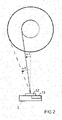
- Figure 2 depicts the dependence of the field of illumination of the emitter 12 on the mode of operation by the driver 13. A smaller angle of half aperture ⁇ 1 is obtained when the driving current is high, and a larger angle of half aperture ⁇ 2 is obtained when the driving current is low.
- the corresponding concentric circles illustrate the different cross sections of the beam across its optical axis.
- the described application of a single light source for different fields of illumination enables a substantial reduction of the complexity and size of a device that is suitable for both time-of-flight measurements and proximity or ambient light measurements.
Landscapes
- Physics & Mathematics (AREA)
- Engineering & Computer Science (AREA)
- General Physics & Mathematics (AREA)
- Electromagnetism (AREA)
- Computer Networks & Wireless Communication (AREA)
- Radar, Positioning & Navigation (AREA)
- Remote Sensing (AREA)
- Optics & Photonics (AREA)
- Condensed Matter Physics & Semiconductors (AREA)
- Life Sciences & Earth Sciences (AREA)
- Sustainable Development (AREA)
- Spectroscopy & Molecular Physics (AREA)
- Optical Radar Systems And Details Thereof (AREA)
Description
- The present disclosure applies to the field of time-of-flight measurement in combination with proximity or ambient light measurements.
- The distance of an object can be measured by the time-of-flight (TOF) method, which determines the time elapsed between the emission of a light signal and the reception of the same light signal after its reflection at the object. A vertical-cavity surface-emitting laser (VCSEL) can be used as emitter, and the arrival of the reflected signal can be detected by a photodetector.
- The field of illumination that is required for proximity measurements is wider than the field of illumination that is required for long-distance time-of-flight measurements. A light-emitting diode (LED) has a relatively wide field of illumination and is appropriate for proximity measurements, whereas a vertical-cavity surface-emitting laser has a comparatively narrow field of illumination in its lasing mode and is appropriate for a time-of-flight measurement. Therefore an arrangement of different sources of electromagnetic radiation, in particular a light-emitting diode and a vertical-cavity surface-emitting laser, which are integrated in two discrete semiconductor dies, may be required within the same package if time-of-flight and proximity measurements are both desired.
-
EP 2 827 175 A2 -
US 2013/0207970 A1 discloses a mapping apparatus comprising a transmitter for emission of a beam comprising light pulses. A scanner is configured to scan the beam over a scene. A processor is coupled to control the scanner so as to cause the beam to scan over a selected window within the scan range and to process the output of a receiver detecting the reflected light by time-of-flight measurement. -
WO 2016/162236 A1 discloses a safe laser device for optical sensing applications. The laser device comprises several mesas. Depending on the structure of the mesas the output power of the laser device is altered. Furthermore, the output power can be controlled by an electric input power supplied to the laser device. The device can be employed for time-of-flight measurements. - It is an object of the present invention to facilitate the performance of alternative time-of-flight and proximity measurements, and to reduce the package size of a time-of-flight device that also allows proximity measurements.
- This object is achieved with the semiconductor device according to
claim 1 and with the method for time-of-flight and proximity measurements according toclaim 9. Embodiments and variants derive from the dependent claims. - The definitions as described above also apply to the following description unless stated otherwise.
- The semiconductor device comprises an emitter of electromagnetic radiation, the emitter being configured for modes of operation providing fields of illumination of different widths, and a photodetector configured for time-of-flight and proximity measurements by detecting electromagnetic radiation that is emitted by the emitter and reflected to the photodetector. The emitter is operated by a driver, which is configured for an alternation between the modes of operation.
- In an embodiment of the semiconductor device, the emitter is a vertical-cavity surface-emitting laser (VCSEL). The driver is configured to generate driving currents for the vertical-cavity surface-emitting laser, one of the driving currents being below a lasing threshold, and one of the driving currents being above the lasing threshold.
- In a further embodiment, the photodetector is part of a photodetector device comprising a semiconductor die, and the emitter is part of an emitter device comprising a further semiconductor die. The driver may especially be integrated in the emitter device. Alternatively, the driver may be integrated in the photodetector device.
- In a further embodiment, an integrated circuit of the photodetector device is configured for performing and evaluating time-of-flight measurements and proximity or ambient light measurements using the emitter and the photodetector.
- In a further embodiment, a carrier is provided to carry the photodetector device and the emitter device, and a cover with windows is mounted on the carrier to cover the photodetector device and the emitter device, the windows being arranged above the photodetector and the emitter.
- In a further embodiment, the driver is configured to switch the modes of operation when values of varying distances that are detected by a time-of-flight or proximity measurement pass a predescribed limit value.
- The method for time-of-flight and proximity measurements comprises operating an emitter of electromagnetic radiation alternatively in different modes of operation providing fields of illumination of different widths, and performing a time-of-flight measurement when the field of illumination is narrow, and a proximity or ambient light measurement when the field of illumination is wide.
- A vertical-cavity surface-emitting laser can be used as emitter, and a driver can be employed to generate driving currents, one of the driving currents being below the lasing threshold of the vertical-cavity surface-emitting laser and one of the driving currents being above the lasing threshold.
- In applications of the method using a vertical-cavity surface-emitting laser and a driver, the proximity or ambient light measurement is performed when the driving currents is below the lasing threshold, and the time-of-flight measurement is performed when the driving currents is above the lasing threshold of the vertical-cavity surface-emitting laser.
- In variants of the method, the different modes of operation are switched when values of varying distances that are detected by a time-of-flight or proximity measurement pass a predescribed limit value.
- The following is a detailed description of examples of the semiconductor device and the method for time-of-flight and proximity measurements in conjunction with the appended figures.
- Figure 1
- shows a semiconductor device including emitter, driver and photodetector.
- Figure 2
- depicts the dependence of the field of illumination of the emitter on the mode of operation.
-
Figure 1 is a cross section of a semiconductor device comprising aphotodetector device 1 and anemitter device 2 in a common package. Theemitter device 2 is a single die with anemitter 12, which is provided as a source of electromagnetic radiation for alternative performances of time-of-flight and proximity measurements. In particular, theemitter 12 may be a vertical-cavity surface-emitting laser (VCSEL) . - A
driver 13, which may especially be integrated in theemitter device 2, enables an alternative operation of theemitter 12 in different modes. Thus either a narrow field of illumination can be achieved, especially by generating a collimated laser beam, or a wider field of illumination, which resembles the field of illumination of a light-emitting diode (LED). A laser beam can be generated by operating a vertical-cavity surface-emitting laser above its lasing threshold. If the vertical-cavity surface-emitting laser is instead driven below its lasing threshold, the emitted light is not narrowly confined, but spread in a wide field of illumination. - For time-of-flight measurements, the vertical-cavity surface-emitting laser is operated above the lasing threshold with very short pulses, which may typically have a duration in the order of magnitude of one hundred picoseconds (300 ps, for instance). For proximity or ambient light measurements, the vertical-cavity surface-emitting laser is operated below the lasing threshold with longer pulses, which may typically have a duration in the order of magnitude of microseconds (ps), to obtain a higher intensity of emission. The
driver 13 may especially be configured for an application of long pulses of currents of less than 200 mA, typically 15 - 20 mA, and short pulses of currents of typically 200 mA or more. - The
driver 13 may also be configured for an automatic switching between time-of-flight measurement and proximity measurement at a predefined limit value of the detected distances. Thedriver 13 can in particular be configured to switch from time-of-flight measurement to proximity measurement, when the values of the varying distances detected by the time-of-flight measurement decrease rapidly and/or below a predefined limit value. For applications in a mobile phone, a distance of typically 10 cm, for instance, may be an appropriate limit value. - The package of the device shown in
Figure 1 includes acarrier 3, on which thephotodetector device 1 and theemitter device 2 are mounted, and acover 4 withwindows 5 above thephotodetector 11 and theemitter 12.Electric connections 6 between contacts of thephotodetector device 1, contacts of theemitter device 2, and further conductors provided in the package are schematically indicated by a bonding wire. - Contacts for external electric connections and/or conductor tracks may also be provided, particularly in the
carrier 3 and on the rear side of thecarrier 3, opposite thephotodetector device 1 and theemitter device 2. Electric connections of semiconductor packages are known per se and can be provided according to the requirements of individual applications. -
Figure 1 shows examples of two different light beams, which can alternatively be generated and emitted by theemitter 12. The solid angle ofemission 7 is smaller for a collimated beam, which is indicated inFigure 1 by a horizontal hatching. Such a beam can be generated by a vertical-cavity surface-emitting laser driven in the lasing mode. The solid angle ofemission 7 is essentially larger when such anemitter 12 is driven below its lasing threshold. An example of a wide beam is shown inFigure 1 with a vertical hatching. - The beam may additionally be shaped by optical components, which may be arranged above the
emitter 12, in particular in thewindow 5. A lens may be particularly favourable if long distances are to be measured by the time-of-flight method. - When the beam is reflected at an
object 8, and reflectedbeams 9 enter thephotodetector 11 through thewindow 5, a time-of-flight measurement or a proximity measurement can be performed, in accordance with the width of the field of illumination that is provided by the operation of theemitter 12 by thedriver 13. - An optical component may be arranged above the
photodetector 11, in particular in thewindow 5, according to the requirements of individual applications. A filter may be desired to shield ambient light that is not emitted by theemitter 12 and reflected by theobject 8. - The
photodetector device 1 may be provided with anintegrated circuit 10 for the operation of thephotodetector 11 and the evaluation of a measurement. Theintegrated circuit 10 may also be configured to address thedriver 13 according to the measured value of the distance of the reflectingobject 8, in order to trigger the switching between the modes of operation of theemitter 12. -
Figure 2 depicts the dependence of the field of illumination of theemitter 12 on the mode of operation by thedriver 13. A smaller angle of half aperture α1 is obtained when the driving current is high, and a larger angle of half aperture α2 is obtained when the driving current is low. The corresponding concentric circles illustrate the different cross sections of the beam across its optical axis. - The described application of a single light source for different fields of illumination enables a substantial reduction of the complexity and size of a device that is suitable for both time-of-flight measurements and proximity or ambient light measurements.
-
- 1
- photodetector device
- 2
- emitter device
- 3
- carrier
- 4
- cover
- 5
- window
- 6
- electric connection
- 7
- solid angle of emission
- 8
- reflecting object
- 9
- reflected beam
- 10
- integrated circuit
- 11
- photodetector
- 12
- emitter
- 13
- driver
- α1
- first angle of half aperture
- α2
- second angle of half aperture
Claims (9)
- A semiconductor device, comprising:an emitter (12) of electromagnetic radiation, the emitter (12) being configured for modes of operation providing fields of illumination of different widths, wherein the emitter (12) is a vertical-cavity surface-emitting laser and the emitter (12) is operated by a driver (13), which is configured for an alternation between the modes of operation, anda photodetector (11) configured for time-of-flight andproximity measurements by detecting electromagnetic radiation that is emitted by the emitter (12) and reflected to the photodetector (11),characterized in thatthe driver (13) is configured to generate driving currents, one of the driving currents being below a lasing threshold of the emitter (12), and one of the driving currents being above the lasing threshold, andthe driver (13) is configured to perform proximity or ambient light measurements by emitted light when the driving current is below the lasing threshold, and to perform time-of-flight measurements by emitted light when the driving current is above the lasing threshold of the vertical-cavity surface-emitting laser.
- The semiconductor device of claim 1, further comprising:a photodetector device (1) comprising a semiconductor die, the photodetector (11) being part of the photodetector device (1), andan emitter device (2) comprising a further semiconductor die, the emitter (12) being part of the emitter device (2).
- The semiconductor device of claim 2, further comprising: an integrated circuit (10) of the photodetector device (1), the integrated circuit (10) being configured for performing and evaluating time-of-flight measurements and proximity or ambient light measurements using the emitter (12) and the photodetector (11).
- The semiconductor device of claim 2 or 3, wherein the driver (13) is integrated in the emitter device (2).
- The semiconductor device of one of claims 2 to 4, further comprising:a carrier (3) carrying the photodetector device (1) and the emitter device (2), anda cover (4) with windows (5), the windows (5) being arranged above the photodetector (11) and the emitter (12).
- The semiconductor device of one of claims 1 to 5, wherein the driver (13) is configured to switch the modes of operation when values of varying distances that are detected by a time-of-flight or proximity measurement pass a predescribed limit value.
- A method of using the semiconductor device of claim 1 for time-of-flight and proximity measurements, comprising:operating the emitter (12) of electromagnetic radiation alternatively in different modes of operation providing fields of illumination of different widths,using a vertical-cavity surface-emitting laser as the emitter (12),using the driver (13) to generate driving currents for the emitter (12), one of the driving currents being below a lasing threshold of the emitter (12) and one of the driving currents being above the lasing threshold, andperforming a time-of-flight measurement when the field of illumination is narrow by operating the vertical-cavity surface-emitting laser above its lasing threshold, and a proximity or ambient light measurement when the field of illumination is wide by driving the vertical-cavity surface-emitting laser below its lasing threshold.
- The method of claim 7, wherein the proximity or ambient light measurement is performed when the driving current is below the lasing threshold of the emitter (12), and the time-of-flight measurement is performed when the driving current is above the lasing threshold of the emitter (12).
- The method of one of claims 7 to 8, wherein the different modes of operation are switched when values of varying distances that are detected by a time-of-flight or proximity measurement pass a predescribed limit value.
Priority Applications (4)
| Application Number | Priority Date | Filing Date | Title |
|---|---|---|---|
| EP17205180.7A EP3493339B1 (en) | 2017-12-04 | 2017-12-04 | Semiconductor device and method for time-of-flight and proximity measurements |
| US16/767,888 US11688998B2 (en) | 2017-12-04 | 2018-12-03 | Semiconductor devices and methods for time-of-flight and proximity measurements |
| CN201880073553.6A CN111837302B (en) | 2017-12-04 | 2018-12-03 | Semiconductor device and method for time-of-flight and proximity measurement |
| PCT/EP2018/083349 WO2019110507A1 (en) | 2017-12-04 | 2018-12-03 | Semiconductor device and method for time-of-flight and proximity measurements |
Applications Claiming Priority (1)
| Application Number | Priority Date | Filing Date | Title |
|---|---|---|---|
| EP17205180.7A EP3493339B1 (en) | 2017-12-04 | 2017-12-04 | Semiconductor device and method for time-of-flight and proximity measurements |
Publications (2)
| Publication Number | Publication Date |
|---|---|
| EP3493339A1 EP3493339A1 (en) | 2019-06-05 |
| EP3493339B1 true EP3493339B1 (en) | 2022-11-09 |
Family
ID=60574448
Family Applications (1)
| Application Number | Title | Priority Date | Filing Date |
|---|---|---|---|
| EP17205180.7A Active EP3493339B1 (en) | 2017-12-04 | 2017-12-04 | Semiconductor device and method for time-of-flight and proximity measurements |
Country Status (4)
| Country | Link |
|---|---|
| US (1) | US11688998B2 (en) |
| EP (1) | EP3493339B1 (en) |
| CN (1) | CN111837302B (en) |
| WO (1) | WO2019110507A1 (en) |
Families Citing this family (1)
| Publication number | Priority date | Publication date | Assignee | Title |
|---|---|---|---|---|
| CN119644342A (en) * | 2023-09-18 | 2025-03-18 | 华为终端有限公司 | Sensor module and electronic equipment |
Family Cites Families (7)
| Publication number | Priority date | Publication date | Assignee | Title |
|---|---|---|---|---|
| CN101897089B (en) * | 2007-12-11 | 2013-02-06 | 皇家飞利浦电子股份有限公司 | Semiconductor laser with integrated phototransistor |
| US9157790B2 (en) * | 2012-02-15 | 2015-10-13 | Apple Inc. | Integrated optoelectronic modules with transmitter, receiver and beam-combining optics for aligning a beam axis with a collection axis |
| US9267787B2 (en) * | 2013-03-15 | 2016-02-23 | Apple Inc. | Depth scanning with multiple emitters |
| US20140268105A1 (en) * | 2013-03-15 | 2014-09-18 | Zygo Corporation | Optical defect inspection system |
| US20150260830A1 (en) * | 2013-07-12 | 2015-09-17 | Princeton Optronics Inc. | 2-D Planar VCSEL Source for 3-D Imaging |
| WO2016096647A1 (en) * | 2014-12-19 | 2016-06-23 | Koninklijke Philips N.V. | Laser sensor module |
| BR112017021395A2 (en) * | 2015-04-10 | 2018-07-03 | Koninklijke Philips Nv | laser device, laser module, optical sensor, mobile communication device, and method of manufacturing a laser device |
-
2017
- 2017-12-04 EP EP17205180.7A patent/EP3493339B1/en active Active
-
2018
- 2018-12-03 CN CN201880073553.6A patent/CN111837302B/en active Active
- 2018-12-03 WO PCT/EP2018/083349 patent/WO2019110507A1/en not_active Ceased
- 2018-12-03 US US16/767,888 patent/US11688998B2/en active Active
Also Published As
| Publication number | Publication date |
|---|---|
| CN111837302B (en) | 2023-09-01 |
| EP3493339A1 (en) | 2019-06-05 |
| WO2019110507A1 (en) | 2019-06-13 |
| US11688998B2 (en) | 2023-06-27 |
| CN111837302A (en) | 2020-10-27 |
| US20210003704A1 (en) | 2021-01-07 |
Similar Documents
| Publication | Publication Date | Title |
|---|---|---|
| CN108351413B (en) | Compact chip-level LIDAR solution | |
| EP3309581B1 (en) | Apparatus for controlling driver current for illumination source | |
| EP3064957B1 (en) | Semiconductor laser driving apparatus, optical scanning apparatus, object detection apparatus, and mobile apparatus | |
| JP6413960B2 (en) | Distance measuring device | |
| JP6340852B2 (en) | Distance measuring device, moving body, and distance measuring method | |
| EP3540468B1 (en) | Object detector, mobile object, and object detection method | |
| CN117607838B (en) | Multichannel driving system, laser radar and laser radar transmitting end driving method | |
| JP2017219502A (en) | Object detection device, sensing device, and mobile device | |
| US12061291B2 (en) | Systems and methods for controlling laser power in light detection and ranging (LiDAR) systems | |
| US20190242981A1 (en) | Target detecting device | |
| JP2017161321A (en) | Circuit device, photodetector, object detection device, sensing device, moving body device, signal detection method, and object detection method | |
| JP7052068B2 (en) | Receiver for receiving optical signals | |
| EP3444634B1 (en) | Semiconductor device and method for time-of-flight measurements | |
| JP2019109193A (en) | Distance measuring device, mobile device and distance measuring | |
| US11688998B2 (en) | Semiconductor devices and methods for time-of-flight and proximity measurements | |
| CN114415192B (en) | Laser radar system and calibration method thereof | |
| US11982744B2 (en) | Operating method and control unit for a LIDAR system, LIDAR system, and device | |
| CN110596675A (en) | Laser emission device and laser radar system | |
| JP2016014577A (en) | Distance measuring device, moving body, and distance measuring method | |
| JP2018040656A (en) | Distance measuring device | |
| CN110662979B (en) | Transmitter unit for emitting radiation into the surrounding environment | |
| JP2015165196A (en) | Distance measuring device, mobile body, and distance measuring method | |
| KR102695035B1 (en) | Laser diode driver | |
| KR20190143332A (en) | Beam projector module for preventing malfunction of eye-safety function, and control method thereof | |
| WO2023225834A1 (en) | Laser radar using light interference |
Legal Events
| Date | Code | Title | Description |
|---|---|---|---|
| PUAI | Public reference made under article 153(3) epc to a published international application that has entered the european phase |
Free format text: ORIGINAL CODE: 0009012 |
|
| STAA | Information on the status of an ep patent application or granted ep patent |
Free format text: STATUS: THE APPLICATION HAS BEEN PUBLISHED |
|
| AK | Designated contracting states |
Kind code of ref document: A1 Designated state(s): AL AT BE BG CH CY CZ DE DK EE ES FI FR GB GR HR HU IE IS IT LI LT LU LV MC MK MT NL NO PL PT RO RS SE SI SK SM TR |
|
| AX | Request for extension of the european patent |
Extension state: BA ME |
|
| STAA | Information on the status of an ep patent application or granted ep patent |
Free format text: STATUS: REQUEST FOR EXAMINATION WAS MADE |
|
| 17P | Request for examination filed |
Effective date: 20191105 |
|
| RBV | Designated contracting states (corrected) |
Designated state(s): AL AT BE BG CH CY CZ DE DK EE ES FI FR GB GR HR HU IE IS IT LI LT LU LV MC MK MT NL NO PL PT RO RS SE SI SK SM TR |
|
| STAA | Information on the status of an ep patent application or granted ep patent |
Free format text: STATUS: EXAMINATION IS IN PROGRESS |
|
| 17Q | First examination report despatched |
Effective date: 20200331 |
|
| GRAP | Despatch of communication of intention to grant a patent |
Free format text: ORIGINAL CODE: EPIDOSNIGR1 |
|
| STAA | Information on the status of an ep patent application or granted ep patent |
Free format text: STATUS: GRANT OF PATENT IS INTENDED |
|
| INTG | Intention to grant announced |
Effective date: 20220704 |
|
| GRAS | Grant fee paid |
Free format text: ORIGINAL CODE: EPIDOSNIGR3 |
|
| GRAA | (expected) grant |
Free format text: ORIGINAL CODE: 0009210 |
|
| STAA | Information on the status of an ep patent application or granted ep patent |
Free format text: STATUS: THE PATENT HAS BEEN GRANTED |
|
| AK | Designated contracting states |
Kind code of ref document: B1 Designated state(s): AL AT BE BG CH CY CZ DE DK EE ES FI FR GB GR HR HU IE IS IT LI LT LU LV MC MK MT NL NO PL PT RO RS SE SI SK SM TR |
|
| REG | Reference to a national code |
Ref country code: GB Ref legal event code: FG4D |
|
| REG | Reference to a national code |
Ref country code: CH Ref legal event code: EP Ref country code: AT Ref legal event code: REF Ref document number: 1530975 Country of ref document: AT Kind code of ref document: T Effective date: 20221115 |
|
| REG | Reference to a national code |
Ref country code: DE Ref legal event code: R096 Ref document number: 602017063482 Country of ref document: DE |
|
| REG | Reference to a national code |
Ref country code: IE Ref legal event code: FG4D |
|
| REG | Reference to a national code |
Ref country code: LT Ref legal event code: MG9D |
|
| REG | Reference to a national code |
Ref country code: NL Ref legal event code: MP Effective date: 20221109 |
|
| REG | Reference to a national code |
Ref country code: AT Ref legal event code: MK05 Ref document number: 1530975 Country of ref document: AT Kind code of ref document: T Effective date: 20221109 |
|
| PG25 | Lapsed in a contracting state [announced via postgrant information from national office to epo] |
Ref country code: SE Free format text: LAPSE BECAUSE OF FAILURE TO SUBMIT A TRANSLATION OF THE DESCRIPTION OR TO PAY THE FEE WITHIN THE PRESCRIBED TIME-LIMIT Effective date: 20221109 Ref country code: PT Free format text: LAPSE BECAUSE OF FAILURE TO SUBMIT A TRANSLATION OF THE DESCRIPTION OR TO PAY THE FEE WITHIN THE PRESCRIBED TIME-LIMIT Effective date: 20230309 Ref country code: NO Free format text: LAPSE BECAUSE OF FAILURE TO SUBMIT A TRANSLATION OF THE DESCRIPTION OR TO PAY THE FEE WITHIN THE PRESCRIBED TIME-LIMIT Effective date: 20230209 Ref country code: LT Free format text: LAPSE BECAUSE OF FAILURE TO SUBMIT A TRANSLATION OF THE DESCRIPTION OR TO PAY THE FEE WITHIN THE PRESCRIBED TIME-LIMIT Effective date: 20221109 Ref country code: FI Free format text: LAPSE BECAUSE OF FAILURE TO SUBMIT A TRANSLATION OF THE DESCRIPTION OR TO PAY THE FEE WITHIN THE PRESCRIBED TIME-LIMIT Effective date: 20221109 Ref country code: ES Free format text: LAPSE BECAUSE OF FAILURE TO SUBMIT A TRANSLATION OF THE DESCRIPTION OR TO PAY THE FEE WITHIN THE PRESCRIBED TIME-LIMIT Effective date: 20221109 Ref country code: AT Free format text: LAPSE BECAUSE OF FAILURE TO SUBMIT A TRANSLATION OF THE DESCRIPTION OR TO PAY THE FEE WITHIN THE PRESCRIBED TIME-LIMIT Effective date: 20221109 |
|
| PG25 | Lapsed in a contracting state [announced via postgrant information from national office to epo] |
Ref country code: RS Free format text: LAPSE BECAUSE OF FAILURE TO SUBMIT A TRANSLATION OF THE DESCRIPTION OR TO PAY THE FEE WITHIN THE PRESCRIBED TIME-LIMIT Effective date: 20221109 Ref country code: PL Free format text: LAPSE BECAUSE OF FAILURE TO SUBMIT A TRANSLATION OF THE DESCRIPTION OR TO PAY THE FEE WITHIN THE PRESCRIBED TIME-LIMIT Effective date: 20221109 Ref country code: LV Free format text: LAPSE BECAUSE OF FAILURE TO SUBMIT A TRANSLATION OF THE DESCRIPTION OR TO PAY THE FEE WITHIN THE PRESCRIBED TIME-LIMIT Effective date: 20221109 Ref country code: IS Free format text: LAPSE BECAUSE OF FAILURE TO SUBMIT A TRANSLATION OF THE DESCRIPTION OR TO PAY THE FEE WITHIN THE PRESCRIBED TIME-LIMIT Effective date: 20230309 Ref country code: HR Free format text: LAPSE BECAUSE OF FAILURE TO SUBMIT A TRANSLATION OF THE DESCRIPTION OR TO PAY THE FEE WITHIN THE PRESCRIBED TIME-LIMIT Effective date: 20221109 Ref country code: GR Free format text: LAPSE BECAUSE OF FAILURE TO SUBMIT A TRANSLATION OF THE DESCRIPTION OR TO PAY THE FEE WITHIN THE PRESCRIBED TIME-LIMIT Effective date: 20230210 |
|
| PG25 | Lapsed in a contracting state [announced via postgrant information from national office to epo] |
Ref country code: NL Free format text: LAPSE BECAUSE OF FAILURE TO SUBMIT A TRANSLATION OF THE DESCRIPTION OR TO PAY THE FEE WITHIN THE PRESCRIBED TIME-LIMIT Effective date: 20221109 |
|
| PG25 | Lapsed in a contracting state [announced via postgrant information from national office to epo] |
Ref country code: SM Free format text: LAPSE BECAUSE OF FAILURE TO SUBMIT A TRANSLATION OF THE DESCRIPTION OR TO PAY THE FEE WITHIN THE PRESCRIBED TIME-LIMIT Effective date: 20221109 Ref country code: RO Free format text: LAPSE BECAUSE OF FAILURE TO SUBMIT A TRANSLATION OF THE DESCRIPTION OR TO PAY THE FEE WITHIN THE PRESCRIBED TIME-LIMIT Effective date: 20221109 Ref country code: EE Free format text: LAPSE BECAUSE OF FAILURE TO SUBMIT A TRANSLATION OF THE DESCRIPTION OR TO PAY THE FEE WITHIN THE PRESCRIBED TIME-LIMIT Effective date: 20221109 Ref country code: DK Free format text: LAPSE BECAUSE OF FAILURE TO SUBMIT A TRANSLATION OF THE DESCRIPTION OR TO PAY THE FEE WITHIN THE PRESCRIBED TIME-LIMIT Effective date: 20221109 Ref country code: CZ Free format text: LAPSE BECAUSE OF FAILURE TO SUBMIT A TRANSLATION OF THE DESCRIPTION OR TO PAY THE FEE WITHIN THE PRESCRIBED TIME-LIMIT Effective date: 20221109 |
|
| REG | Reference to a national code |
Ref country code: CH Ref legal event code: PL |
|
| REG | Reference to a national code |
Ref country code: DE Ref legal event code: R097 Ref document number: 602017063482 Country of ref document: DE |
|
| REG | Reference to a national code |
Ref country code: BE Ref legal event code: MM Effective date: 20221231 |
|
| PG25 | Lapsed in a contracting state [announced via postgrant information from national office to epo] |
Ref country code: SK Free format text: LAPSE BECAUSE OF FAILURE TO SUBMIT A TRANSLATION OF THE DESCRIPTION OR TO PAY THE FEE WITHIN THE PRESCRIBED TIME-LIMIT Effective date: 20221109 Ref country code: LU Free format text: LAPSE BECAUSE OF NON-PAYMENT OF DUE FEES Effective date: 20221204 Ref country code: AL Free format text: LAPSE BECAUSE OF FAILURE TO SUBMIT A TRANSLATION OF THE DESCRIPTION OR TO PAY THE FEE WITHIN THE PRESCRIBED TIME-LIMIT Effective date: 20221109 |
|
| PLBE | No opposition filed within time limit |
Free format text: ORIGINAL CODE: 0009261 |
|
| STAA | Information on the status of an ep patent application or granted ep patent |
Free format text: STATUS: NO OPPOSITION FILED WITHIN TIME LIMIT |
|
| P01 | Opt-out of the competence of the unified patent court (upc) registered |
Effective date: 20230822 |
|
| 26N | No opposition filed |
Effective date: 20230810 |
|
| GBPC | Gb: european patent ceased through non-payment of renewal fee |
Effective date: 20230209 |
|
| PG25 | Lapsed in a contracting state [announced via postgrant information from national office to epo] |
Ref country code: LI Free format text: LAPSE BECAUSE OF NON-PAYMENT OF DUE FEES Effective date: 20221231 Ref country code: IE Free format text: LAPSE BECAUSE OF NON-PAYMENT OF DUE FEES Effective date: 20221204 Ref country code: CH Free format text: LAPSE BECAUSE OF NON-PAYMENT OF DUE FEES Effective date: 20221231 |
|
| PG25 | Lapsed in a contracting state [announced via postgrant information from national office to epo] |
Ref country code: SI Free format text: LAPSE BECAUSE OF FAILURE TO SUBMIT A TRANSLATION OF THE DESCRIPTION OR TO PAY THE FEE WITHIN THE PRESCRIBED TIME-LIMIT Effective date: 20221109 Ref country code: BE Free format text: LAPSE BECAUSE OF NON-PAYMENT OF DUE FEES Effective date: 20221231 |
|
| PG25 | Lapsed in a contracting state [announced via postgrant information from national office to epo] |
Ref country code: GB Free format text: LAPSE BECAUSE OF NON-PAYMENT OF DUE FEES Effective date: 20230209 |
|
| PG25 | Lapsed in a contracting state [announced via postgrant information from national office to epo] |
Ref country code: GB Free format text: LAPSE BECAUSE OF NON-PAYMENT OF DUE FEES Effective date: 20230209 |
|
| PG25 | Lapsed in a contracting state [announced via postgrant information from national office to epo] |
Ref country code: HU Free format text: LAPSE BECAUSE OF FAILURE TO SUBMIT A TRANSLATION OF THE DESCRIPTION OR TO PAY THE FEE WITHIN THE PRESCRIBED TIME-LIMIT; INVALID AB INITIO Effective date: 20171204 |
|
| PG25 | Lapsed in a contracting state [announced via postgrant information from national office to epo] |
Ref country code: CY Free format text: LAPSE BECAUSE OF FAILURE TO SUBMIT A TRANSLATION OF THE DESCRIPTION OR TO PAY THE FEE WITHIN THE PRESCRIBED TIME-LIMIT Effective date: 20221109 |
|
| PG25 | Lapsed in a contracting state [announced via postgrant information from national office to epo] |
Ref country code: MK Free format text: LAPSE BECAUSE OF FAILURE TO SUBMIT A TRANSLATION OF THE DESCRIPTION OR TO PAY THE FEE WITHIN THE PRESCRIBED TIME-LIMIT Effective date: 20221109 Ref country code: IT Free format text: LAPSE BECAUSE OF FAILURE TO SUBMIT A TRANSLATION OF THE DESCRIPTION OR TO PAY THE FEE WITHIN THE PRESCRIBED TIME-LIMIT Effective date: 20221109 |
|
| PG25 | Lapsed in a contracting state [announced via postgrant information from national office to epo] |
Ref country code: MC Free format text: LAPSE BECAUSE OF FAILURE TO SUBMIT A TRANSLATION OF THE DESCRIPTION OR TO PAY THE FEE WITHIN THE PRESCRIBED TIME-LIMIT Effective date: 20221109 |
|
| PG25 | Lapsed in a contracting state [announced via postgrant information from national office to epo] |
Ref country code: MC Free format text: LAPSE BECAUSE OF FAILURE TO SUBMIT A TRANSLATION OF THE DESCRIPTION OR TO PAY THE FEE WITHIN THE PRESCRIBED TIME-LIMIT Effective date: 20221109 |
|
| PG25 | Lapsed in a contracting state [announced via postgrant information from national office to epo] |
Ref country code: BG Free format text: LAPSE BECAUSE OF FAILURE TO SUBMIT A TRANSLATION OF THE DESCRIPTION OR TO PAY THE FEE WITHIN THE PRESCRIBED TIME-LIMIT Effective date: 20221109 |
|
| PG25 | Lapsed in a contracting state [announced via postgrant information from national office to epo] |
Ref country code: MT Free format text: LAPSE BECAUSE OF FAILURE TO SUBMIT A TRANSLATION OF THE DESCRIPTION OR TO PAY THE FEE WITHIN THE PRESCRIBED TIME-LIMIT Effective date: 20221109 |
|
| PG25 | Lapsed in a contracting state [announced via postgrant information from national office to epo] |
Ref country code: TR Free format text: LAPSE BECAUSE OF FAILURE TO SUBMIT A TRANSLATION OF THE DESCRIPTION OR TO PAY THE FEE WITHIN THE PRESCRIBED TIME-LIMIT Effective date: 20221109 |
|
| PGFP | Annual fee paid to national office [announced via postgrant information from national office to epo] |
Ref country code: DE Payment date: 20251211 Year of fee payment: 9 |
|
| PGFP | Annual fee paid to national office [announced via postgrant information from national office to epo] |
Ref country code: FR Payment date: 20251229 Year of fee payment: 9 |
|
| REG | Reference to a national code |
Ref country code: DE Ref legal event code: R081 Ref document number: 602017063482 Country of ref document: DE Owner name: AMS-OSRAM AG, AT Free format text: FORMER OWNER: AMS AG, PREMSTAETTEN, AT |