EP3493248A1 - Self-aligned contact and method for forming the same - Google Patents
Self-aligned contact and method for forming the same Download PDFInfo
- Publication number
- EP3493248A1 EP3493248A1 EP18206639.9A EP18206639A EP3493248A1 EP 3493248 A1 EP3493248 A1 EP 3493248A1 EP 18206639 A EP18206639 A EP 18206639A EP 3493248 A1 EP3493248 A1 EP 3493248A1
- Authority
- EP
- European Patent Office
- Prior art keywords
- forming
- self
- gate structures
- aligned contact
- gate
- Prior art date
- Legal status (The legal status is an assumption and is not a legal conclusion. Google has not performed a legal analysis and makes no representation as to the accuracy of the status listed.)
- Granted
Links
Images





Classifications
-
- H—ELECTRICITY
- H10—SEMICONDUCTOR DEVICES; ELECTRIC SOLID-STATE DEVICES NOT OTHERWISE PROVIDED FOR
- H10D—INORGANIC ELECTRIC SEMICONDUCTOR DEVICES
- H10D64/00—Electrodes of devices having potential barriers
- H10D64/01—Manufacture or treatment
- H10D64/011—Manufacture or treatment of electrodes ohmically coupled to a semiconductor
-
- H—ELECTRICITY
- H10—SEMICONDUCTOR DEVICES; ELECTRIC SOLID-STATE DEVICES NOT OTHERWISE PROVIDED FOR
- H10W—GENERIC PACKAGES, INTERCONNECTIONS, CONNECTORS OR OTHER CONSTRUCTIONAL DETAILS OF DEVICES COVERED BY CLASS H10
- H10W20/00—Interconnections in chips, wafers or substrates
- H10W20/01—Manufacture or treatment
- H10W20/031—Manufacture or treatment of conductive parts of the interconnections
- H10W20/069—Manufacture or treatment of conductive parts of the interconnections by forming self-aligned vias or self-aligned contact plugs
-
- H—ELECTRICITY
- H10—SEMICONDUCTOR DEVICES; ELECTRIC SOLID-STATE DEVICES NOT OTHERWISE PROVIDED FOR
- H10D—INORGANIC ELECTRIC SEMICONDUCTOR DEVICES
- H10D30/00—Field-effect transistors [FET]
- H10D30/01—Manufacture or treatment
- H10D30/021—Manufacture or treatment of FETs having insulated gates [IGFET]
-
- H—ELECTRICITY
- H10—SEMICONDUCTOR DEVICES; ELECTRIC SOLID-STATE DEVICES NOT OTHERWISE PROVIDED FOR
- H10D—INORGANIC ELECTRIC SEMICONDUCTOR DEVICES
- H10D30/00—Field-effect transistors [FET]
- H10D30/60—Insulated-gate field-effect transistors [IGFET]
-
- H—ELECTRICITY
- H10—SEMICONDUCTOR DEVICES; ELECTRIC SOLID-STATE DEVICES NOT OTHERWISE PROVIDED FOR
- H10D—INORGANIC ELECTRIC SEMICONDUCTOR DEVICES
- H10D64/00—Electrodes of devices having potential barriers
- H10D64/01—Manufacture or treatment
- H10D64/017—Manufacture or treatment using dummy gates in processes wherein at least parts of the final gates are self-aligned to the dummy gates, i.e. replacement gate processes
-
- H—ELECTRICITY
- H10—SEMICONDUCTOR DEVICES; ELECTRIC SOLID-STATE DEVICES NOT OTHERWISE PROVIDED FOR
- H10D—INORGANIC ELECTRIC SEMICONDUCTOR DEVICES
- H10D64/00—Electrodes of devices having potential barriers
- H10D64/01—Manufacture or treatment
- H10D64/021—Manufacture or treatment using multiple gate spacer layers, e.g. bilayered sidewall spacers
-
- H—ELECTRICITY
- H10—SEMICONDUCTOR DEVICES; ELECTRIC SOLID-STATE DEVICES NOT OTHERWISE PROVIDED FOR
- H10P—GENERIC PROCESSES OR APPARATUS FOR THE MANUFACTURE OR TREATMENT OF DEVICES COVERED BY CLASS H10
- H10P50/00—Etching of wafers, substrates or parts of devices
- H10P50/20—Dry etching; Plasma etching; Reactive-ion etching
- H10P50/28—Dry etching; Plasma etching; Reactive-ion etching of insulating materials
- H10P50/282—Dry etching; Plasma etching; Reactive-ion etching of insulating materials of inorganic materials
- H10P50/283—Dry etching; Plasma etching; Reactive-ion etching of insulating materials of inorganic materials by chemical means
-
- H—ELECTRICITY
- H10—SEMICONDUCTOR DEVICES; ELECTRIC SOLID-STATE DEVICES NOT OTHERWISE PROVIDED FOR
- H10P—GENERIC PROCESSES OR APPARATUS FOR THE MANUFACTURE OR TREATMENT OF DEVICES COVERED BY CLASS H10
- H10P76/00—Manufacture or treatment of masks on semiconductor bodies, e.g. by lithography or photolithography
- H10P76/40—Manufacture or treatment of masks on semiconductor bodies, e.g. by lithography or photolithography of masks comprising inorganic materials
- H10P76/408—Manufacture or treatment of masks on semiconductor bodies, e.g. by lithography or photolithography of masks comprising inorganic materials characterised by their sizes, orientations, dispositions, behaviours or shapes
- H10P76/4085—Manufacture or treatment of masks on semiconductor bodies, e.g. by lithography or photolithography of masks comprising inorganic materials characterised by their sizes, orientations, dispositions, behaviours or shapes characterised by the processes involved to create the masks
-
- H—ELECTRICITY
- H10—SEMICONDUCTOR DEVICES; ELECTRIC SOLID-STATE DEVICES NOT OTHERWISE PROVIDED FOR
- H10W—GENERIC PACKAGES, INTERCONNECTIONS, CONNECTORS OR OTHER CONSTRUCTIONAL DETAILS OF DEVICES COVERED BY CLASS H10
- H10W20/00—Interconnections in chips, wafers or substrates
- H10W20/01—Manufacture or treatment
- H10W20/031—Manufacture or treatment of conductive parts of the interconnections
- H10W20/069—Manufacture or treatment of conductive parts of the interconnections by forming self-aligned vias or self-aligned contact plugs
- H10W20/0696—Manufacture or treatment of conductive parts of the interconnections by forming self-aligned vias or self-aligned contact plugs by using sacrificial placeholders, e.g. using sacrificial plugs
Definitions
- the disclosure relates to a semiconductor structure and more particularly to a self-aligned contact and a method for forming a self-aligned contact.
- the present disclosure provides a method for forming a self-aligned contact.
- the method includes providing a substrate with a plurality of gate structures including spacers on opposite sides.
- the method also includes forming a sacrificial layer between the gate structures.
- the method also includes forming a mask layer on a part of the sacrificial layer.
- the method also includes forming a plurality of first openings by removing the sacrificial layer exposed from the mask layer.
- the method also includes forming a dielectric layer in the plurality of first openings.
- the method also includes removing the mask layer.
- the method also includes forming a plurality of second openings by removing the sacrificial layer that remains on the substrate.
- the method also includes forming a plurality of first contact plugs in the second openings.
- the present disclosure also provides a self-aligned contact that includes a plurality of gate structures including spacers on opposite sides on a substrate.
- the self-aligned contact also includes a dielectric layer disposed between the gate structures.
- the self-aligned contact also includes a plurality of first contact plugs disposed between the gate structures in the dielectric layer.
- the spacer has a planar top surface.
- first and second features are formed in direct contact
- additional features may be formed between the first and second features, such that the first and second features may not be in direct contact
- present disclosure may repeat reference numerals and/or letters in the various examples. This repetition is for the purpose of simplicity and clarity and does not in itself dictate a relationship between the various embodiments and/or configurations discussed.
- spatially relative terms such as “beneath,” “below,” “lower,” “above,” “upper” and the like, may be used herein for ease of description to describe one element or feature's relationship to other elements or features as illustrated in the figures.
- the spatially relative terms are intended to encompass different orientations of the device in use or operation in addition to the orientation depicted in the figures.
- the apparatus may be otherwise oriented (rotated 90 degrees or at other orientations) and the spatially relative descriptors used herein may likewise be interpreted accordingly.
- the terms “around,” “about,” “substantial” usually mean within 20% of a given value or range, preferably within 10%, and better within 5%, or 3%, or 2%, or 1%, or 0.5%. It should be noted that the quantity herein is a substantial quantity, which means that the meaning of "around,” “about,” “substantial” are still implied even without specific mention of the terms “around,” “about,” “substantial.”
- the embodiments of the present disclosure provide a method of forming a self-aligned contact.
- a self-aligned sacrificial layer right where the contacts between the gate structures will be formed, the contacts formed later may be symmetrical and separate from the gate structures. Therefore, the capacitance between the gate and the drain may be reduced and have less variation.
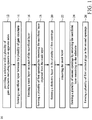
- FIG. 1 is a flow chart of a method 10 for forming a self-aligned contact 100 in accordance with some embodiments.
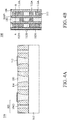
- FIGS. 2A-11A are cross-sectional representations of various stages of forming the self-aligned contact 100 in accordance with some embodiments of the present disclosure.
- FIGS. 2B-11B are top views of various stages of forming the self-aligned contact 100 in accordance with some embodiments of the present disclosure.
- Figures having the suffix "A" e.g., FIG. 2A
- Figures having the suffix "B" are cross-sectional views of some embodiments of the self-aligned contact, taken along line A-A in the figures having the suffix "B" (e.g., FIG. 2B ).
- the embodiments of the present disclosure will be described with reference to the flowchart in FIG. 1 and the cross-sectional views illustrated in FIGS. 2A-11A along with the top views in FIGS. 2B-11B .
- the method 10 begins with step 12, in which a substrate 102 with a plurality of gate structures 103 is provided.
- the gate structures 103 include dummy gates 104D and spacers 106 formed on the opposite sides of the dummy gates 104D.
- the substrate 102 may be a semiconductor substrate such as a Si substrate.
- the semiconductor substrate may also include other elementary semiconductors such as Ge; compound semiconductors such as GaN, SiC, GaAs, GaP, InP, InAs, and/or InSb; alloy semiconductors such as SiGe, GaAsP, AlInAs, AlGaAs, GaInAs, GaInP, and/or GaInAsP, or a combination thereof.
- the substrate 102 has a first conductivity type.
- the substrate 102 has a second conductivity type. The second conductivity type is opposite to the first conductivity type.
- the first conductivity type is P-type.
- the substrate 102 may be a boron-doped substrate.
- the first conductivity type is N-type.
- the substrate 102 may be a phosphorous-doped or arsenic-doped substrate.
- the substrate 102 may also be semiconductor on insulator (SOI).
- gate structures 103 are formed on the substrate 102.
- the gate structures 103 include the dummy gates 104D and the spacers 106 formed on the opposite sidewalls of the dummy gates 104D.
- the dummy gate 104D may include a dummy gate material layer and a dummy cap layer (not shown).
- the dummy gate material layer may include polycrystalline silicon, polycrystalline SiGe, amorphous silicon, microcrystal silicon, another suitable dummy gate material layer, or a combination thereof.
- the dummy cap layer may include silicon nitride.
- the dummy gate material layer may be formed blanketly on the substrate 102 by chemical vapor deposition (CVD) (such as high density plasma chemical vapor deposition (HDPCVD), atmospheric pressure chemical vapor deposition (APCVD), low-pressure chemical vapor deposition (LPCVD), or plasma enhanced chemical vapor deposition (PECVD)), atomic layer deposition (ALD), physical vapor deposition (PVD), electroplating, spin-on coating, another suitable deposition process, or a combination thereof.
- CVD chemical vapor deposition
- HDPCVD high density plasma chemical vapor deposition
- APCVD atmospheric pressure chemical vapor deposition
- LPCVD low-pressure chemical vapor deposition
- PECVD plasma enhanced chemical vapor deposition
- ALD atomic layer deposition
- PVD physical vapor deposition
- electroplating spin-on coating
- the dummy gate 104D is formed by a photolithography and etching process.
- the photolithography process may include photoresist coating (e.g., spin-on coating), soft baking, mask aligning, pattern exposure, post-exposure baking, photoresist development, and rinsing and drying (e.g., hard baking), etc.
- the etching process may include a dry etching process (e.g., reactive ion etching (RIE), anisotropic plasma etching method), a wet etching process, or a combination thereof.
- RIE reactive ion etching
- the spacers 106 are formed on the opposite sides of the dummy gates 104D.
- the spacers 106 may include oxides, nitrides, oxynitrides, a high k material, a low k material, or a combination thereof.
- the precursor material or gaseous reactants of forming the spacers 106 may include TEOS (tetraethoxysilane), TRIES (triethoxysilane), BTBAS (bis(tert-butylamino) silane), O 2 , N 2 O, NO, other gas or materials, or a combination thereof.
- the spacers 106 may be conformally formed on the dummy gates 104D and the substrate 102 by LPCVD, PECVD, HDP-CVD, APCVD, ATD, another suitable deposition method, or a combination thereof. After that, an anisotropic etch-back is performed, and the spacers 106 are remained on the opposite sides of the dummy gate 104D.
- the etch-back may be a dry etch process, which may be performed using an oxygen-containing gas, a fluorine-containing gas (such as CF 4 , SF 6 , CH 2 F 2 , CHF 3 , and/or C 2 F 6 ), a chlorine-containing gas (such as Cl 2 , CHCl 3 , CCl 4 , and/or BCl 3 ), a bromine-containing gas (such as HBr and/or CHBR 3 ), an iodine-containing gas, another suitable gas or plasma, or a combination thereof.
- a fluorine-containing gas such as CF 4 , SF 6 , CH 2 F 2 , CHF 3 , and/or C 2 F 6
- a chlorine-containing gas such as Cl 2 , CHCl 3 , CCl 4 , and/or BCl 3
- a bromine-containing gas such as HBr and/or CHBR 3
- an iodine-containing gas another suitable gas or plasma, or a
- epi regions are formed in the active area of the substrate 102 between the gate structures 103 (now shown).
- epi regions may be P-type.
- P-type epi regions may include SiGe and may be in-situ doped during an epitaxial growth process using P-type dopants such as, boron, indium, or gallium.
- P-type dopants such as, boron, indium, or gallium.
- P-type doping precursors such as diborane (B 2 H 6 ), boron trifluoride (BF 3 ) and/or other P-type doping precursors may be used.
- epi regions may be N-type.
- N-type epi regions may include SiP and may be in-situ doped during an epitaxial growth process using N-type dopants such as, phosphorus or arsenic.
- N-type dopants such as, phosphorus or arsenic.
- n-type doping precursors such as phosphine (PH 3 ), arsine (AsH 3 ), and/or other n-type doping precursor may be used.
- the CESL may include silicon nitride (Si x N y ), silicon oxynitride (SiO x N y ), carbon-doped silicon oxide (SiC x O y ), carbon-doped silicon nitride (SiC x N y ), another suitable material, or a combination thereof.
- the CESL may be conformally formed on the gate structures 103 and the substrate 102 by LPCVD, PECVD, HDP-CVD, APCVD, ATD, another suitable deposition method, or a combination thereof.
- the method 10 proceeds to step 14, in which a sacrificial layer 110 is formed between the gate structures 103.
- the sacrificial layer 110 may include polysilicon, SiGe, doped polysilicon (for example, polysilicon doped by fluorine), doped SiGe (for example, SiGe doped by boron), another material which can be selectively etched in the subsequent process, or a combination thereof.
- the sacrificial layer 110 may be selectively etched relative to oxides and nitrides in the subsequent process.
- the sacrificial layer 110 may be formed on the substrate 102 between the gate structures 103 using chemical vapor deposition (CVD) (such as high density plasma chemical vapor deposition (HDPCVD), atmospheric pressure chemical vapor deposition (APCVD), low-pressure chemical vapor deposition (LPCVD), or plasma enhanced chemical vapor deposition (PECVD)), atomic layer deposition (ALD), physical vapor deposition (PVD), electroplating, spin-on coating, another suitable deposition process, or a combination thereof.
- CVD chemical vapor deposition
- HDPCVD high density plasma chemical vapor deposition
- APCVD atmospheric pressure chemical vapor deposition
- LPCVD low-pressure chemical vapor deposition
- PECVD plasma enhanced chemical vapor deposition
- ALD atomic layer deposition
- PVD physical vapor deposition
- electroplating spin-on coating, another suitable deposition process, or a combination thereof.
- a planarization process such as a chemical mechanical polishing (CMP) process or an etch-back process is performed on the gate structures 103 and the sacrificial layer 110. Since the self-aligned contacts will be formed in the subsequent process in the location where parts of the sacrificial layer 110 is formed, the distance between the sacrificial layer 110 and the dummy gate 104D is critical. If the distance between the sacrificial layer 110 and the dummy gate 104D is too short, it may cause electrical short-circuits or increases in the Cgd capacitance. If the distance between the sacrificial layer 110 and the dummy gate 104D is too long, the contact resistance may increase when the gate pitch is the same.
- CMP chemical mechanical polishing
- the method 10 proceeds to step 16, in which a mask layer 112 is formed on a part of the sacrificial layer 110.
- the mask layer 112 may include silicon nitride, silicon oxide, TiN, other applicable materials, or a combination thereof.
- the mask layer 112 may be formed using a low-pressure chemical vapor deposition (LPCVD) process, a plasma-enhanced chemical vapor deposition (PECVD) process, another suitable process, or a combination thereof.
- LPCVD low-pressure chemical vapor deposition
- PECVD plasma-enhanced chemical vapor deposition
- the mask layer 112 is patterned to form desired patterns between the gate structures 103.
- the process of patterning the mask layer 112 may include a photolithography process and an etching process.
- the photolithography process may include photoresist coating (e.g., spin-on coating), soft baking, mask aligning, exposure, post-exposure baking, developing the photoresist, rinsing and drying (e.g., hard baking).
- the etching process may include a dry etching process (e.g., an anisotropic plasma etching method), a wet etching process, or a combination thereof.
- the mask layer 112 is formed by a single photomask. In some other embodiments, the mask layer 112 is formed by two separate photomasks. For example, as shown in FIG.
- the first portion 112A of the mask layer 112 is formed with a first photomask
- the second portion 112B of the mask layer 112 is formed with a second photomask.
- Forming the mask layer 112 with multiple photomasks is beneficial when the pitch of the mask layer 112 is small, since this method may overcome the limitations of small spaces on the photomasks. It should be noted that, although there are two photomasks used in the embodiments shown in FIG. 4B , the number of photomasks is not limited thereto. More than two photomasks may be used when forming the mask layer 112.
- the method 10 proceeds to step 18, in which the first openings 114 are formed by removing the sacrificial layer 110 exposed from the mask layer 112.
- the sacrificial layer 110 is removed by an etching process.
- the etching process may be a dry etching process, a wet etching process, a reactive ion etching process, or another suitable etching process.
- the dry etching process may be performed using an oxygen-containing gas, a fluorine-containing gas (such as CF 4 , SF 6 , CH 2 F 2 , CHF 3 , and/or C 2 F 6 ), a chlorine-containing gas (such as Cl 2 , CHCl 3 , CCl 4 , and/or BCl 3 ), a bromine-containing gas (such as HBr and/or CHBR 3 ), an iodine-containing gas, another suitable gas or plasma, or a combination thereof.
- a fluorine-containing gas such as CF 4 , SF 6 , CH 2 F 2 , CHF 3 , and/or C 2 F 6
- a chlorine-containing gas such as Cl 2 , CHCl 3 , CCl 4 , and/or BCl 3
- a bromine-containing gas such as HBr and/or CHBR 3
- an iodine-containing gas another suitable gas or plasma, or a combination thereof.
- the wet etching process may be performed in wet-etching etchant such as phosphoric acid based (H3PO4), diluted hydrofluoric acid (DHF), potassium hydroxide (KOH), ammonia, hydrofluoric acid (HF), nitric acid (HNO 3 ), acetic acid (CH 3 COOH), another suitable wet-etching etchant, or a combination thereof.
- wet-etching etchant such as phosphoric acid based (H3PO4), diluted hydrofluoric acid (DHF), potassium hydroxide (KOH), ammonia, hydrofluoric acid (HF), nitric acid (HNO 3 ), acetic acid (CH 3 COOH), another suitable wet-etching etchant, or a combination thereof.
- the photolithography process may include photoresist coating (e.g., spin-on coating), soft baking, mask aligning, pattern exposure, post-exposure baking, photoresist development, and rinsing and drying (e.g., hard baking), etc.
- the etching process may include a dry etching process (e.g., reactive ion etching (RIE), anisotropic plasma etching method), a wet etching process, or a combination thereof.
- RIE reactive ion etching
- the gate structures 103 After parts of the gate structures 103 are removed, some of the first openings 114 may be the same as before, and some of the first openings 114 may be expanded as the first openings 114E shown in FIGS. 6A and 6B .
- the gate structures 103 may be more uniform.
- the method 10 proceeds to step 20, in which a dielectric layer 118 is formed in the first openings 114 and 114E.
- the dielectric layer 118 may include dielectric materials such as silicon oxide, silicon nitride, silicon oxynitride, tetraethoxysilane (TEOS), phosphosilicate glass (PSG), borophosphosilicate glass (BPSG), low-k dielectric material, and/or other applicable dielectric materials.
- low-k dielectric materials include, but are not limited to, fluorinated silica glass (FSG), carbon doped silicon oxide, amorphous fluorinated carbon, parylene, bis-benzocyclobutenes (BCB), polyimide, or a combination thereof.
- the dielectric layer 118 may be formed using a chemical vapor deposition (CVD) process (e.g., a high-density plasma chemical vapor deposition (HDPCVD) process, an atmospheric pressure chemical vapor deposition (APCVD) process, a low-pressure chemical vapor deposition (LPCVD) process, a plasma enhanced chemical vapor deposition (PECVD) process), a spin-on coating process, an atomic layer deposition process, another applicable process, or a combination thereof.
- CVD chemical vapor deposition
- HDPCVD high-density plasma chemical vapor deposition
- APCVD atmospheric pressure chemical vapor deposition
- LPCVD low-pressure chemical vapor deposition
- PECVD plasma enhanced chemical vapor deposition
- spin-on coating process e.g., an atomic layer deposition process, another applicable process, or a combination thereof.
- a planarization process e.g., a chemical mechanical polishing process or an etching back process
- the dummy gates 104D are replaced with a metal gate 104M and an overlying gate cap layer 104C.
- the dummy gates 104D are removed using an anisotropic vertical etch process such as reactive ion etch (RIE) or a dry etching process, and an opening between the spacers 106 is formed (not shown).
- RIE reactive ion etch
- the dry etching process may be performed using an oxygen-containing gas, a fluorine-containing gas (such as CF 4 , SF 6 , CH 2 F 2 , CHF 3 , and/or C 2 F 6 ), a chlorine-containing gas (such as Cl 2 , CHCl 3 , CCl 4 , and/or BCl 3 ), a bromine-containing gas (such as HBr and/or CHBR 3 ), an iodine-containing gas, another suitable gas or plasma, or a combination thereof.
- a gate dielectric layer is then formed in the opening between the spacers 106 (not shown).
- the gate dielectric layer may include silicon oxide.
- the silicon oxide may be formed using an oxidation process (e.g., a dry oxidation process or a wet oxidation process), a chemical vapor deposition process, another applicable process, or a combination thereof.
- the gate dielectric layer may include a high-k dielectric layer (e.g., one with a dielectric constant that is greater than 3.9) such as hafnium oxide (HfO 2 ).
- the high-k dielectric layer may include other high-k dielectrics, such as LaO, AlO, ZrO, TiO, Ta 2 O 5 , Y 2 O 3 , SrTiO 3 , BaTiO 3 , BaZrO, HfZrO, HfLaO, HfTaO, HfSiO, HfSiON, HfTiO, LaSiO, AlSiO, (Ba, Sr)TiO 3 , Al 2 O 3 , or a combination thereof.
- other high-k dielectrics such as LaO, AlO, ZrO, TiO, Ta 2 O 5 , Y 2 O 3 , SrTiO 3 , BaTiO 3 , BaZrO, HfZrO, HfLaO, HfTaO, HfSiO, HfSiON, HfTiO, LaSiO, AlSiO, (Ba, Sr)TiO 3 , Al 2 O 3
- the high-k dielectric layer may be formed using a chemical vapor deposition process (e.g., a plasma enhanced chemical vapor deposition (PECVD) process or a metalorganic chemical vapor deposition (MOCVD) process), an atomic layer deposition (ALD) process (e.g., a plasma enhanced atomic layer deposition (PEALD) process), a physical vapor deposition (PVD) process (e.g., a vacuum evaporation process or a sputtering process), another applicable process, or a combination thereof.
- a chemical vapor deposition process e.g., a plasma enhanced chemical vapor deposition (PECVD) process or a metalorganic chemical vapor deposition (MOCVD) process
- ALD atomic layer deposition
- PVD physical vapor deposition
- a vacuum evaporation process or a sputtering process another applicable process, or a combination thereof.
- metal gate 104M is formed in the opening between the spacers 106 on the gate dielectric layer.
- the metal gate 104M may include metal gate materials such as a single layer of TiN, TaN, TaAlC, TiC, TaC, Co, Al, TiAl, HfTi, TiSi, TaSi, or TiAlC, or two or more layers thereof.
- metal gate materials such as a single layer of TiN, TaN, TaAlC, TiC, TaC, Co, Al, TiAl, HfTi, TiSi, TaSi, or TiAlC, or two or more layers thereof.
- TaN, TaAlC, TiN, TiC, Co, TiAl, HfTi, TiSi, and TaSi may be formed as the metal gate 104M.
- the metal gate 104M may be formed by conformally depositing the metal gate materials in the opening between the spacers 106 using a chemical vapor deposition process (e.g., a low-pressure chemical vapor deposition process or a plasma enhanced chemical vapor deposition process), a physical vapor deposition process (e.g., a vacuum evaporation process or a sputtering process), another applicable process, or a combination thereof.
- a chemical vapor deposition process e.g., a low-pressure chemical vapor deposition process or a plasma enhanced chemical vapor deposition process
- a physical vapor deposition process e.g., a vacuum evaporation process or a sputtering process
- the metal gate material is then recessed to form a recess in the opening between the spacers 106 (not shown).
- a gate cap layer 104C is formed in the recess between the spacers 106 on the metal gate 104M.
- the gate cap layer 104C may include silicon nitride.
- the gate cap layer 104C may be formed on the metal gate 104M by low-pressure chemical vapor deposition (LPCVD), plasma enhanced chemical vapor deposition (PECVD), another suitable deposition process, or a combination thereof.
- LPCVD low-pressure chemical vapor deposition
- PECVD plasma enhanced chemical vapor deposition
- a planarization process e.g., a chemical mechanical polishing process or an etching back process
- the method 10 proceeds to step 22, in which the mask layer 112 is removed.
- the mask layer may be removed using an etching process such as a dry etching process (e.g., an anisotropic plasma etching method), a wet etching process, or a combination thereof.
- a dry etching process e.g., an anisotropic plasma etching method
- a wet etching process e.g., a Bosch plasma etching method
- step 24 in which second openings 120 are formed by removing the sacrificial layer 110 remaining on the substrate 102.
- the sacrificial layer 110 is removed using a selective etching process relative to the dielectric layer 118, the gate cap layer 104C, and the spacers 106.
- the sacrificial layer 110 is removed using a selective etching process relative to oxide and nitride.
- the etching process may include a dry etching process, a wet etching process, a reactive ion etching process, or another suitable etching process.
- the dry etching process may be performed using an oxygen-containing gas, a fluorine-containing gas (such as CF 4 , SF 6 , CH 2 F 2 , CHF 3 , and/or C 2 F 6 ), a chlorine-containing gas (such as Cl 2 , CHCl 3 , CCl 4 , and/or BCl 3 ), a bromine-containing gas (such as HBr and/or CHBR 3 ), an iodine-containing gas, another suitable gas or plasma, or a combination thereof.
- a fluorine-containing gas such as CF 4 , SF 6 , CH 2 F 2 , CHF 3 , and/or C 2 F 6
- a chlorine-containing gas such as Cl 2 , CHCl 3 , CCl 4 , and/or BCl 3
- a bromine-containing gas such as HBr and/or CHBR 3
- an iodine-containing gas another suitable gas or plasma, or a combination thereof.
- the wet etching process may be performed in wet-etching etchant such as diluted hydrofluoric acid (DHF), potassium hydroxide (KOH), ammonia, hydrofluoric acid (HF), nitric acid (HNO 3 ), acetic acid (CH 3 COOH), another suitable wet-etching etchant, or a combination thereof. Since the sacrificial layer 110 is removed using a selective etching process, the dielectric layer 118, the gate cap layer 104C, and the spacers 106 may not be damaged during the selective etching process.
- wet-etching etchant such as diluted hydrofluoric acid (DHF), potassium hydroxide (KOH), ammonia, hydrofluoric acid (HF), nitric acid (HNO 3 ), acetic acid (CH 3 COOH), another suitable wet-etching etchant, or a combination thereof. Since the sacrificial layer 110 is removed using a selective etching process, the dielectric layer
- first contact plugs 122 are formed in the second openings 120.
- the first contact plugs 122 can be made of metal materials (e.g., W, Al, or Cu), metal alloys, poly-Si, other applicable conductive materials, and combinations thereof.
- the first contact plugs 122 can be formed by using a chemical vapor deposition process (CVD), a physical vapor deposition process (PVD, e.g., evaporation or sputtering), an atomic layer deposition process (ALD), an electroplating process, another suitable process, or a combination thereof to deposit the conductive materials of the first contact structure, and then optionally performing a chemical mechanical polishing (CMP) process or an etching back process to remove the excess conductive materials.
- CVD chemical vapor deposition process
- PVD physical vapor deposition process
- ALD atomic layer deposition process
- electroplating process another suitable process, or a combination thereof
- CMP chemical mechanical polishing
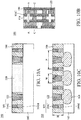
- FIG. 10C is a cross-sectional view of some embodiments of the self-aligned contact, taken along line C-C in FIG. 10B .
- epi regions 108 are formed in the active area of the substrate 102 between the gate structures 103.
- the first contact plugs 122 formed between the gate structures 103 are symmetrical. If the first contact plugs 122 are not symmetrical between the gate structures 103, the distance between the first contact plugs 122 and the gate structures 103 may be shorter on one side, and the capacitance between the gate and the drain may increase. Variations of the capacitance may also be minimized by using symmetrical first contact plugs 122.
- the spacers 106 may have a planar top surface and the first contact plugs 122 are not formed on the top of the spacers 106. This may keep the first contact plugs 122 apart from the metal gate 104M and the gate cap layer 104C and may help to decrease the capacitance between the gate and the drain.
- the angle ⁇ between the sidewalls and the top surface of the first contact plugs 122 is greater than 70 °. preferably is substantially 90°. When the angle ⁇ is too small, the distance between the first contact plugs 122 and the metal gate 104M and the gate cap layer 104C may be too close, and the capacitance between the gate and the drain may increase.
- the maximum width W of the first contact plugs 122 is less than or equal to 33% of the pitch P of the gate structures 103. If the maximum width W of the first contact plugs 122 is too wide, which means the first contact plugs 122 are too close to the metal gate 104M and the gate cap layer 104C, the capacitance between the gate and the drain may increase. Therefore, using the method for forming the self-aligned contact 100 that was described above, the first contact plugs 122 are apart from the metal gate 104M and the gate cap layer 104C. Short-circuits may be prevented and the capacitance between the gate and the drain is decreased and has less variation. Moreover, in some embodiments, the gate structures 103 have a height H (including the height of the gate cap layer 104C), which is in a range of 100% to 150% of the pitch P of the gate structures 103.
- FIG. 11C is a cross-sectional view of some embodiments of the self-aligned contact, taken along line C-C in FIG. 11B .
- the second contact plugs 124 may include Ti, Al, Au, Pd, Cu, W, another suitable metal, metal alloys, poly-Si, another applicable conductive material, or a combination thereof. As shown in FIG.
- the gate cap layer 104C is removed and a recess is formed, and then the contact material is formed in the recess and on the gate structures 103 first by chemical vapor deposition (CVD), physical vapor deposition (PVD) (e.g., resistive heating evaporation or sputtering), electroplating, atomic layer deposition (ALD), another suitable method, or a combination thereof.
- CVD chemical vapor deposition
- PVD physical vapor deposition
- ALD atomic layer deposition
- the electrode material is then patterned using a photolithography and etching process to form the second contact plugs 124.
- a dielectric layer 126 is formed surrounding the second contact plugs 124.
- dielectric layer 126 Some processes and materials used to form the dielectric layer 126 may be similar to, or the same as, those used to form the dielectric layer 118 and are not repeated herein. For the purpose of clarity, the dielectric layer 126 is not shown in FIG. 11B and the structures underneath are presented.
- a method of forming a self-aligned contact is provided.
- the size of the contacts may be controlled and the contacts may be kept apart from the gate structures. Therefore, the capacitance between the gate and the drain may be reduced and capacitance variations may be minimized.
Landscapes
- Internal Circuitry In Semiconductor Integrated Circuit Devices (AREA)
- Insulated Gate Type Field-Effect Transistor (AREA)
- Electrodes Of Semiconductors (AREA)
Abstract
Description
- This application claims the benefit of
U.S. Provisional Application No. 62/592,543 filed on November 30, 2017 - The disclosure relates to a semiconductor structure and more particularly to a self-aligned contact and a method for forming a self-aligned contact.
- The semiconductor integrated circuit industry has experienced rapid growth. The development of integrated-circuit design and advancements in materials technology have produced generations of integrated circuits. Each generation has smaller and more complex circuits than the previous one. In the process of integrated-circuit development, geometric size has gradually reduced.
- As integrated circuits have shrunk, the space between contact structures has decreased. Therefore, a self-aligned contact (SAC) process has been applied to prevent the contacts from short-circuiting. However, this may increase the capacitance between the gate and the drain (Cgd). Moreover, variations in the self-aligned contact structure may also cause a variation of the capacitance between the gate and the drain.
- Although existing self-aligned contacts have generally been adequate for their intended purposes, they have not been entirely satisfactory in all respects, and need to be improved. This is especially true of the control of the capacitance between the gate and the drain with self-aligned contacts.
- The present disclosure provides a method for forming a self-aligned contact. The method includes providing a substrate with a plurality of gate structures including spacers on opposite sides. The method also includes forming a sacrificial layer between the gate structures. The method also includes forming a mask layer on a part of the sacrificial layer. The method also includes forming a plurality of first openings by removing the sacrificial layer exposed from the mask layer. The method also includes forming a dielectric layer in the plurality of first openings. The method also includes removing the mask layer. The method also includes forming a plurality of second openings by removing the sacrificial layer that remains on the substrate. The method also includes forming a plurality of first contact plugs in the second openings.
- The present disclosure also provides a self-aligned contact that includes a plurality of gate structures including spacers on opposite sides on a substrate. The self-aligned contact also includes a dielectric layer disposed between the gate structures. The self-aligned contact also includes a plurality of first contact plugs disposed between the gate structures in the dielectric layer. The spacer has a planar top surface.
- A detailed description is given in the following embodiments with reference to the accompanying drawings.
- Aspects of the present disclosure are best understood from the following detailed description when read with the accompanying figures. It should be noted that, in accordance with the standard practice in the industry, various features are not drawn to scale. In fact, the dimensions of the various features may be arbitrarily increased or reduced for clarity of discussion.
-
FIG. 1 is a flow chart of a method for forming a self-aligned contact in accordance with some embodiments. -
FIGS. 2A-11A are cross-sectional representations of various stages of forming a self-aligned contact in accordance with some embodiments. -
FIGS. 2B-11B are top views of various stages of forming a self-aligned contact in accordance with some embodiments. -
FIGS. 10C and11C are cross-sectional representations of a self-aligned contact in accordance with some embodiments. - The following disclosure provides many different embodiments, or examples, for implementing different features of the disclosure. Specific examples of components and arrangements are described below to simplify the present disclosure. These are, of course, merely examples and are not intended to be limiting. For example, the formation of a first feature over or on a second feature in the description that follows may include embodiments in which the first and second features are formed in direct contact, and may also include embodiments in which additional features may be formed between the first and second features, such that the first and second features may not be in direct contact. In addition, the present disclosure may repeat reference numerals and/or letters in the various examples. This repetition is for the purpose of simplicity and clarity and does not in itself dictate a relationship between the various embodiments and/or configurations discussed.
- Furthermore, spatially relative terms, such as "beneath," "below," "lower," "above," "upper" and the like, may be used herein for ease of description to describe one element or feature's relationship to other elements or features as illustrated in the figures. The spatially relative terms are intended to encompass different orientations of the device in use or operation in addition to the orientation depicted in the figures. The apparatus may be otherwise oriented (rotated 90 degrees or at other orientations) and the spatially relative descriptors used herein may likewise be interpreted accordingly.
- Herein, the terms "around," "about," "substantial" usually mean within 20% of a given value or range, preferably within 10%, and better within 5%, or 3%, or 2%, or 1%, or 0.5%. It should be noted that the quantity herein is a substantial quantity, which means that the meaning of "around," "about," "substantial" are still implied even without specific mention of the terms "around," "about," "substantial."
- Although some embodiments are discussed with operations performed in a particular order, these operations may be performed in another logical order. In different embodiments, additional operations can be provided before, during, and/or after the stages described the present disclosure. Some of the stages that are described can be replaced or eliminated for different embodiments. Additional features can be added to the semiconductor structure in the present disclosure. Some of the features described below can be replaced or eliminated for different embodiments.
- The embodiments of the present disclosure provide a method of forming a self-aligned contact. By forming a self-aligned sacrificial layer right where the contacts between the gate structures will be formed, the contacts formed later may be symmetrical and separate from the gate structures. Therefore, the capacitance between the gate and the drain may be reduced and have less variation.
-
FIG. 1 is a flow chart of amethod 10 for forming a self-alignedcontact 100 in accordance with some embodiments.FIGS. 2A-11A are cross-sectional representations of various stages of forming the self-alignedcontact 100 in accordance with some embodiments of the present disclosure.FIGS. 2B-11B are top views of various stages of forming the self-alignedcontact 100 in accordance with some embodiments of the present disclosure. Figures having the suffix "A" (e.g.,FIG. 2A ) are cross-sectional views of some embodiments of the self-aligned contact, taken along line A-A in the figures having the suffix "B" (e.g.,FIG. 2B ). In the following paragraphs, the embodiments of the present disclosure will be described with reference to the flowchart inFIG. 1 and the cross-sectional views illustrated inFIGS. 2A-11A along with the top views inFIGS. 2B-11B . - As shown in
FIGS. 1 ,2A, and 2B , themethod 10 begins withstep 12, in which asubstrate 102 with a plurality ofgate structures 103 is provided. Thegate structures 103 includedummy gates 104D and spacers 106 formed on the opposite sides of thedummy gates 104D. - In some embodiments, the
substrate 102 may be a semiconductor substrate such as a Si substrate. Moreover, the semiconductor substrate may also include other elementary semiconductors such as Ge; compound semiconductors such as GaN, SiC, GaAs, GaP, InP, InAs, and/or InSb; alloy semiconductors such as SiGe, GaAsP, AlInAs, AlGaAs, GaInAs, GaInP, and/or GaInAsP, or a combination thereof. In some embodiments, thesubstrate 102 has a first conductivity type. In some other embodiments, thesubstrate 102 has a second conductivity type. The second conductivity type is opposite to the first conductivity type. In some embodiments, the first conductivity type is P-type. For example, thesubstrate 102 may be a boron-doped substrate. In some other embodiments, the first conductivity type is N-type. For example, thesubstrate 102 may be a phosphorous-doped or arsenic-doped substrate. In some embodiments, thesubstrate 102 may also be semiconductor on insulator (SOI). - Next,
gate structures 103 are formed on thesubstrate 102. Thegate structures 103 include thedummy gates 104D and thespacers 106 formed on the opposite sidewalls of thedummy gates 104D. In some embodiments, thedummy gate 104D may include a dummy gate material layer and a dummy cap layer (not shown). The dummy gate material layer may include polycrystalline silicon, polycrystalline SiGe, amorphous silicon, microcrystal silicon, another suitable dummy gate material layer, or a combination thereof. The dummy cap layer may include silicon nitride. In some embodiments, the dummy gate material layer may be formed blanketly on thesubstrate 102 by chemical vapor deposition (CVD) (such as high density plasma chemical vapor deposition (HDPCVD), atmospheric pressure chemical vapor deposition (APCVD), low-pressure chemical vapor deposition (LPCVD), or plasma enhanced chemical vapor deposition (PECVD)), atomic layer deposition (ALD), physical vapor deposition (PVD), electroplating, spin-on coating, another suitable deposition process, or a combination thereof. The dummy cap layer may be formed blanketly on the dummy gate material layer by low-pressure chemical vapor deposition (LPCVD), plasma enhanced chemical vapor deposition (PECVD), another suitable deposition process, or a combination thereof. - After that, the
dummy gate 104D is formed by a photolithography and etching process. The photolithography process may include photoresist coating (e.g., spin-on coating), soft baking, mask aligning, pattern exposure, post-exposure baking, photoresist development, and rinsing and drying (e.g., hard baking), etc. The etching process may include a dry etching process (e.g., reactive ion etching (RIE), anisotropic plasma etching method), a wet etching process, or a combination thereof. - In some embodiments, the
spacers 106 are formed on the opposite sides of thedummy gates 104D. In some embodiments, thespacers 106 may include oxides, nitrides, oxynitrides, a high k material, a low k material, or a combination thereof. The precursor material or gaseous reactants of forming thespacers 106 may include TEOS (tetraethoxysilane), TRIES (triethoxysilane), BTBAS (bis(tert-butylamino) silane), O2, N2O, NO, other gas or materials, or a combination thereof. Thespacers 106 may be conformally formed on thedummy gates 104D and thesubstrate 102 by LPCVD, PECVD, HDP-CVD, APCVD, ATD, another suitable deposition method, or a combination thereof. After that, an anisotropic etch-back is performed, and thespacers 106 are remained on the opposite sides of thedummy gate 104D. In some embodiments, the etch-back may be a dry etch process, which may be performed using an oxygen-containing gas, a fluorine-containing gas (such as CF4, SF6, CH2F2, CHF3, and/or C2F6), a chlorine-containing gas (such as Cl2, CHCl3, CCl4, and/or BCl3), a bromine-containing gas (such as HBr and/or CHBR3), an iodine-containing gas, another suitable gas or plasma, or a combination thereof. - Next, epi regions are formed in the active area of the
substrate 102 between the gate structures 103 (now shown). In some embodiments, epi regions may be P-type. P-type epi regions may include SiGe and may be in-situ doped during an epitaxial growth process using P-type dopants such as, boron, indium, or gallium. For P-type in-situ doping, P-type doping precursors such as diborane (B2H6), boron trifluoride (BF3) and/or other P-type doping precursors may be used. In some other embodiments, epi regions may be N-type. N-type epi regions may include SiP and may be in-situ doped during an epitaxial growth process using N-type dopants such as, phosphorus or arsenic. For N-type in-situ doping, n-type doping precursors such as phosphine (PH3), arsine (AsH3), and/or other n-type doping precursor may be used. - Next, a contact etch stop layer (CESL) is formed on the
gate structures 103 and the substrate 102 (not shown). In some embodiments, the CESL may include silicon nitride (SixNy), silicon oxynitride (SiOxNy), carbon-doped silicon oxide (SiCxOy), carbon-doped silicon nitride (SiCxNy), another suitable material, or a combination thereof. The CESL may be conformally formed on thegate structures 103 and thesubstrate 102 by LPCVD, PECVD, HDP-CVD, APCVD, ATD, another suitable deposition method, or a combination thereof. - Next, as shown in
FIGS. 1 ,3A, and 3B , themethod 10 proceeds to step 14, in which asacrificial layer 110 is formed between thegate structures 103. In some embodiments, thesacrificial layer 110 may include polysilicon, SiGe, doped polysilicon (for example, polysilicon doped by fluorine), doped SiGe (for example, SiGe doped by boron), another material which can be selectively etched in the subsequent process, or a combination thereof. In some embodiments, thesacrificial layer 110 may be selectively etched relative to oxides and nitrides in the subsequent process. In some embodiments, thesacrificial layer 110 may be formed on thesubstrate 102 between thegate structures 103 using chemical vapor deposition (CVD) (such as high density plasma chemical vapor deposition (HDPCVD), atmospheric pressure chemical vapor deposition (APCVD), low-pressure chemical vapor deposition (LPCVD), or plasma enhanced chemical vapor deposition (PECVD)), atomic layer deposition (ALD), physical vapor deposition (PVD), electroplating, spin-on coating, another suitable deposition process, or a combination thereof. - Next, a planarization process such as a chemical mechanical polishing (CMP) process or an etch-back process is performed on the
gate structures 103 and thesacrificial layer 110. Since the self-aligned contacts will be formed in the subsequent process in the location where parts of thesacrificial layer 110 is formed, the distance between thesacrificial layer 110 and thedummy gate 104D is critical. If the distance between thesacrificial layer 110 and thedummy gate 104D is too short, it may cause electrical short-circuits or increases in the Cgd capacitance. If the distance between thesacrificial layer 110 and thedummy gate 104D is too long, the contact resistance may increase when the gate pitch is the same. - Next, as shown in
FIGS. 1 ,4A, and 4B , themethod 10 proceeds to step 16, in which amask layer 112 is formed on a part of thesacrificial layer 110. In some embodiments, themask layer 112 may include silicon nitride, silicon oxide, TiN, other applicable materials, or a combination thereof. Themask layer 112 may be formed using a low-pressure chemical vapor deposition (LPCVD) process, a plasma-enhanced chemical vapor deposition (PECVD) process, another suitable process, or a combination thereof. In some embodiments, as shown inFIG. 4B , themask layer 112 is patterned to form desired patterns between thegate structures 103. The process of patterning themask layer 112 may include a photolithography process and an etching process. The photolithography process may include photoresist coating (e.g., spin-on coating), soft baking, mask aligning, exposure, post-exposure baking, developing the photoresist, rinsing and drying (e.g., hard baking). The etching process may include a dry etching process (e.g., an anisotropic plasma etching method), a wet etching process, or a combination thereof. In some embodiments, themask layer 112 is formed by a single photomask. In some other embodiments, themask layer 112 is formed by two separate photomasks. For example, as shown inFIG. 4B , thefirst portion 112A of themask layer 112 is formed with a first photomask, and thesecond portion 112B of themask layer 112 is formed with a second photomask. Forming themask layer 112 with multiple photomasks is beneficial when the pitch of themask layer 112 is small, since this method may overcome the limitations of small spaces on the photomasks. It should be noted that, although there are two photomasks used in the embodiments shown inFIG. 4B , the number of photomasks is not limited thereto. More than two photomasks may be used when forming themask layer 112. - Next, as shown in
FIGS. 1 ,5A, and 5B , themethod 10 proceeds to step 18, in which thefirst openings 114 are formed by removing thesacrificial layer 110 exposed from themask layer 112. In some embodiments, thesacrificial layer 110 is removed by an etching process. The etching process may be a dry etching process, a wet etching process, a reactive ion etching process, or another suitable etching process. In some embodiments, the dry etching process may be performed using an oxygen-containing gas, a fluorine-containing gas (such as CF4, SF6, CH2F2, CHF3, and/or C2F6), a chlorine-containing gas (such as Cl2, CHCl3, CCl4, and/or BCl3), a bromine-containing gas (such as HBr and/or CHBR3), an iodine-containing gas, another suitable gas or plasma, or a combination thereof. In some embodiments, the wet etching process may be performed in wet-etching etchant such as phosphoric acid based (H3PO4), diluted hydrofluoric acid (DHF), potassium hydroxide (KOH), ammonia, hydrofluoric acid (HF), nitric acid (HNO3), acetic acid (CH3COOH), another suitable wet-etching etchant, or a combination thereof. - Next, as shown in
FIGS. 6A and 6B , parts of thegate structures 103 are removed to form the desired pattern on thegate structures 103 from a top view. Parts of thegate structures 103 are removed in a photolithography and etching process. The photolithography process may include photoresist coating (e.g., spin-on coating), soft baking, mask aligning, pattern exposure, post-exposure baking, photoresist development, and rinsing and drying (e.g., hard baking), etc. The etching process may include a dry etching process (e.g., reactive ion etching (RIE), anisotropic plasma etching method), a wet etching process, or a combination thereof. After parts of thegate structures 103 are removed, some of thefirst openings 114 may be the same as before, and some of thefirst openings 114 may be expanded as thefirst openings 114E shown inFIGS. 6A and 6B . By removing parts of thegate structures 103 to form the desired pattern of thegate structures 103 instead of forming the desired pattern of thegate structures 103 directly, thegate structures 103 may be more uniform. - Next, as shown in
FIGS. 1 ,7A, and 7B , themethod 10 proceeds to step 20, in which adielectric layer 118 is formed in thefirst openings dielectric layer 118 may include dielectric materials such as silicon oxide, silicon nitride, silicon oxynitride, tetraethoxysilane (TEOS), phosphosilicate glass (PSG), borophosphosilicate glass (BPSG), low-k dielectric material, and/or other applicable dielectric materials. Examples of low-k dielectric materials include, but are not limited to, fluorinated silica glass (FSG), carbon doped silicon oxide, amorphous fluorinated carbon, parylene, bis-benzocyclobutenes (BCB), polyimide, or a combination thereof. Thedielectric layer 118 may be formed using a chemical vapor deposition (CVD) process (e.g., a high-density plasma chemical vapor deposition (HDPCVD) process, an atmospheric pressure chemical vapor deposition (APCVD) process, a low-pressure chemical vapor deposition (LPCVD) process, a plasma enhanced chemical vapor deposition (PECVD) process), a spin-on coating process, an atomic layer deposition process, another applicable process, or a combination thereof. After thedielectric layer 118 is deposited, a planarization process (e.g., a chemical mechanical polishing process or an etching back process) may optionally be performed to remove the excess dielectric materials. - Next, as shown in
FIG. 7A and 7B , thedummy gates 104D are replaced with ametal gate 104M and an overlyinggate cap layer 104C. Thedummy gates 104D are removed using an anisotropic vertical etch process such as reactive ion etch (RIE) or a dry etching process, and an opening between thespacers 106 is formed (not shown). In some embodiments, the dry etching process may be performed using an oxygen-containing gas, a fluorine-containing gas (such as CF4, SF6, CH2F2, CHF3, and/or C2F6), a chlorine-containing gas (such as Cl2, CHCl3, CCl4, and/or BCl3), a bromine-containing gas (such as HBr and/or CHBR3), an iodine-containing gas, another suitable gas or plasma, or a combination thereof. A gate dielectric layer is then formed in the opening between the spacers 106 (not shown). The gate dielectric layer may include silicon oxide. The silicon oxide may be formed using an oxidation process (e.g., a dry oxidation process or a wet oxidation process), a chemical vapor deposition process, another applicable process, or a combination thereof. Alternatively, the gate dielectric layer may include a high-k dielectric layer (e.g., one with a dielectric constant that is greater than 3.9) such as hafnium oxide (HfO2). Alternatively, the high-k dielectric layer may include other high-k dielectrics, such as LaO, AlO, ZrO, TiO, Ta2O5, Y2O3, SrTiO3, BaTiO3, BaZrO, HfZrO, HfLaO, HfTaO, HfSiO, HfSiON, HfTiO, LaSiO, AlSiO, (Ba, Sr)TiO3, Al2O3, or a combination thereof. The high-k dielectric layer may be formed using a chemical vapor deposition process (e.g., a plasma enhanced chemical vapor deposition (PECVD) process or a metalorganic chemical vapor deposition (MOCVD) process), an atomic layer deposition (ALD) process (e.g., a plasma enhanced atomic layer deposition (PEALD) process), a physical vapor deposition (PVD) process (e.g., a vacuum evaporation process or a sputtering process), another applicable process, or a combination thereof. - Next,
metal gate 104M is formed in the opening between thespacers 106 on the gate dielectric layer. Themetal gate 104M may include metal gate materials such as a single layer of TiN, TaN, TaAlC, TiC, TaC, Co, Al, TiAl, HfTi, TiSi, TaSi, or TiAlC, or two or more layers thereof. For an N-type FET, one or more layers of TaN, TaAlC, TiN, TiC, Co, TiAl, HfTi, TiSi, and TaSi may be formed as themetal gate 104M. For a P-type FET, one or more layers of TiAlC, Al, TiAl, TaN, TaAlC, TiN, TiC, or Co may be formed as themetal gate 104M. In some embodiments, themetal gate 104M may be formed by conformally depositing the metal gate materials in the opening between thespacers 106 using a chemical vapor deposition process (e.g., a low-pressure chemical vapor deposition process or a plasma enhanced chemical vapor deposition process), a physical vapor deposition process (e.g., a vacuum evaporation process or a sputtering process), another applicable process, or a combination thereof. In some embodiments, the metal gate material is then recessed to form a recess in the opening between the spacers 106 (not shown). - Next, a
gate cap layer 104C is formed in the recess between thespacers 106 on themetal gate 104M. Thegate cap layer 104C may include silicon nitride. In some embodiments, thegate cap layer 104C may be formed on themetal gate 104M by low-pressure chemical vapor deposition (LPCVD), plasma enhanced chemical vapor deposition (PECVD), another suitable deposition process, or a combination thereof. After thegate cap layer 104C is deposited, a planarization process (e.g., a chemical mechanical polishing process or an etching back process) may optionally be performed to remove the excess dielectric materials. - Next, as shown in
FIGS. 1 ,8A, and 8B , themethod 10 proceeds to step 22, in which themask layer 112 is removed. The mask layer may be removed using an etching process such as a dry etching process (e.g., an anisotropic plasma etching method), a wet etching process, or a combination thereof. After themask layer 112 is removed, thesacrificial layer 110 remaining on thesubstrate 120 is exposed. - Next, as shown in
FIGS. 1 ,9A, and 9B , themethod 10 proceeds to step 24, in whichsecond openings 120 are formed by removing thesacrificial layer 110 remaining on thesubstrate 102. In some embodiments, thesacrificial layer 110 is removed using a selective etching process relative to thedielectric layer 118, thegate cap layer 104C, and thespacers 106. For example, thesacrificial layer 110 is removed using a selective etching process relative to oxide and nitride. The etching process may include a dry etching process, a wet etching process, a reactive ion etching process, or another suitable etching process. In some embodiments, the dry etching process may be performed using an oxygen-containing gas, a fluorine-containing gas (such as CF4, SF6, CH2F2, CHF3, and/or C2F6), a chlorine-containing gas (such as Cl2, CHCl3, CCl4, and/or BCl3), a bromine-containing gas (such as HBr and/or CHBR3), an iodine-containing gas, another suitable gas or plasma, or a combination thereof. In some embodiments, the wet etching process may be performed in wet-etching etchant such as diluted hydrofluoric acid (DHF), potassium hydroxide (KOH), ammonia, hydrofluoric acid (HF), nitric acid (HNO3), acetic acid (CH3COOH), another suitable wet-etching etchant, or a combination thereof. Since thesacrificial layer 110 is removed using a selective etching process, thedielectric layer 118, thegate cap layer 104C, and thespacers 106 may not be damaged during the selective etching process. - Next, as shown in
FIGS. 1 ,10A, and 10B , themethod 10 proceeds to step 24, in which first contact plugs 122 are formed in thesecond openings 120. The first contact plugs 122 can be made of metal materials (e.g., W, Al, or Cu), metal alloys, poly-Si, other applicable conductive materials, and combinations thereof. The first contact plugs 122 can be formed by using a chemical vapor deposition process (CVD), a physical vapor deposition process (PVD, e.g., evaporation or sputtering), an atomic layer deposition process (ALD), an electroplating process, another suitable process, or a combination thereof to deposit the conductive materials of the first contact structure, and then optionally performing a chemical mechanical polishing (CMP) process or an etching back process to remove the excess conductive materials. -
FIG. 10C is a cross-sectional view of some embodiments of the self-aligned contact, taken along line C-C inFIG. 10B . As shown inFIG. 10C ,epi regions 108 are formed in the active area of thesubstrate 102 between thegate structures 103. As shown inFIG. 10C , the first contact plugs 122 formed between thegate structures 103 are symmetrical. If the first contact plugs 122 are not symmetrical between thegate structures 103, the distance between the first contact plugs 122 and thegate structures 103 may be shorter on one side, and the capacitance between the gate and the drain may increase. Variations of the capacitance may also be minimized by using symmetrical first contact plugs 122. In addition, thespacers 106 may have a planar top surface and the first contact plugs 122 are not formed on the top of thespacers 106. This may keep the first contact plugs 122 apart from themetal gate 104M and thegate cap layer 104C and may help to decrease the capacitance between the gate and the drain. Moreover, the angle θ between the sidewalls and the top surface of the first contact plugs 122 is greater than 70 °. preferably is substantially 90°. When the angle θ is too small, the distance between the first contact plugs 122 and themetal gate 104M and thegate cap layer 104C may be too close, and the capacitance between the gate and the drain may increase. In addition, the maximum width W of the first contact plugs 122 is less than or equal to 33% of the pitch P of thegate structures 103. If the maximum width W of the first contact plugs 122 is too wide, which means the first contact plugs 122 are too close to themetal gate 104M and thegate cap layer 104C, the capacitance between the gate and the drain may increase. Therefore, using the method for forming the self-alignedcontact 100 that was described above, the first contact plugs 122 are apart from themetal gate 104M and thegate cap layer 104C. Short-circuits may be prevented and the capacitance between the gate and the drain is decreased and has less variation. Moreover, in some embodiments, thegate structures 103 have a height H (including the height of thegate cap layer 104C), which is in a range of 100% to 150% of the pitch P of thegate structures 103. - Next, as shown in
FIGS. 11A-11C , second contact plugs 124 are formed on thegate structures 103 and the first contact plugs 122.FIG. 11C is a cross-sectional view of some embodiments of the self-aligned contact, taken along line C-C inFIG. 11B . In some embodiments, the second contact plugs 124 may include Ti, Al, Au, Pd, Cu, W, another suitable metal, metal alloys, poly-Si, another applicable conductive material, or a combination thereof. As shown inFIG. 11C according to some embodiments, thegate cap layer 104C is removed and a recess is formed, and then the contact material is formed in the recess and on thegate structures 103 first by chemical vapor deposition (CVD), physical vapor deposition (PVD) (e.g., resistive heating evaporation or sputtering), electroplating, atomic layer deposition (ALD), another suitable method, or a combination thereof. The electrode material is then patterned using a photolithography and etching process to form the second contact plugs 124. Next, as shown inFIGS. 11A and 11C , adielectric layer 126 is formed surrounding the second contact plugs 124. Some processes and materials used to form thedielectric layer 126 may be similar to, or the same as, those used to form thedielectric layer 118 and are not repeated herein. For the purpose of clarity, thedielectric layer 126 is not shown inFIG. 11B and the structures underneath are presented. - As mentioned above, in the present disclosure, a method of forming a self-aligned contact is provided. With a self-aligned sacrificial layer formed at the positions where the contacts between the gate structures are to be formed, the size of the contacts may be controlled and the contacts may be kept apart from the gate structures. Therefore, the capacitance between the gate and the drain may be reduced and capacitance variations may be minimized.
- It should be noted that although some of the benefits and effects are described in the embodiments above, not every embodiment needs to achieve all the benefits and effects.
- The foregoing outlines features of several embodiments so that those skilled in the art may better understand the aspects of the present disclosure. Those skilled in the art should appreciate that they may readily use the present disclosure as a basis for designing or modifying other processes and structures for carrying out the same purposes and/or achieving the same advantages of the embodiments introduced herein. Those skilled in the art should also realize that such equivalent constructions do not depart from the spirit and scope of the present disclosure, and that they may make various changes, substitutions, and alterations herein without departing from the spirit and scope of the present disclosure.
Claims (15)
- A method for forming a self-aligned contact, comprising:providing a substrate with a plurality of gate structures including spacers on opposite sides;forming a sacrificial layer between the plurality of gate structures;forming a mask layer on a part of the sacrificial layer;forming a plurality of first openings by removing the sacrificial layer exposed from the mask layer;forming a dielectric layer in the plurality of first openings;removing the mask layer;forming a plurality of second openings by removing the sacrificial layer remaining on the substrate; andforming a plurality of first contact plugs in the second openings.
- The method for forming a self-aligned contact as claimed in claim 1, wherein forming the second openings comprises selectively etching the sacrificial layer relative to the dielectric layer.
- The method for forming a self-aligned contact as claimed in claim 1 or 2, further comprising:performing a planarization process on the gate structures and the sacrificial layer before forming the mask layer.
- The method for forming a self-aligned contact as claimed in one of the preceding claims, wherein a height of the gate structures is in a range of 100% to 150% of a pitch of the gate structures, and/or
wherein the spacer has a planar top surface. - The method for forming a self-aligned contact as claimed in one of the preceding claims, wherein an angle between any portion of sidewalls and a top surface of the first contact plugs is greater than 70°, and/or
wherein a maximum width of the first contact plugs is less than or equal to 33% of a pitch of the gate structures. - The method for forming a self-aligned contact as claimed in one of the preceding claims, wherein the sacrificial layer comprises polysilicon, SiGe, doped polysilicon, doped SiGe, or a combination thereof.
- The method for forming a self-aligned contact as claimed in one of the preceding claims, further comprising:removing parts of the gate structures after removal of the sacrificial layer exposed from the mask layer.
- The method for forming a self-aligned contact as claimed in one of the preceding claims, further comprising:replacing the gate structures with a metal gate after the dielectric layer is formed,wherein a gate cap layer is formed on the metal gate.
- The method for forming a self-aligned contact as claimed in one of the preceding claims, wherein forming the mask layer comprises:forming a first portion of the mask layer using a first patterning process with a first photomask; andforming a second portion of the mask layer using a second patterning process with a second photomask.
- The method for forming a self-aligned contact as claimed in claim 1, wherein the dielectric layer comprises silicon oxide, silicon nitride, silicon oxynitride, tetraethoxysilane (TEOS), phosphosilicate glass (PSG), borophosphosilicate glass (BPSG), fluorinated silica glass (FSG), carbon doped silicon oxide, amorphous fluorinated carbon, parylene, bis-benzocyclobutenes (BCB), polyimide, or a combination thereof, and/or wherein the method further comprises:forming a plurality of second contact plugs on the gate structures.
- A self-aligned contact, comprising:a plurality of gate structures including spacers on opposite sides on a substrate;a dielectric layer disposed between the gate structures; anda plurality of first contact plugs disposed between the gate structures in the dielectric layer;wherein the spacer has a planar top surface.
- The self-aligned contact as claimed in claim 11, wherein the plurality of the contact plugs between the gate structures are symmetrical, and/or
wherein an angle between any portion of sidewalls and a top surface of the first contact plugs is greater than 70°. - The self-aligned contact as claimed in claim 11 or 12, wherein a maximum width of the first contact plugs is less than or equal to 33% of a pitch of the gate structures, and/or wherein a height of the gate structures is in a range of 100% to 150% of a pitch of the gate structures.
- The self-aligned contact as claimed in one of claims 11 to 13, wherein each of the gate structures comprises a gate cap layer on a metal gate.
- The self-aligned contact as claimed in one of claims 11 to 14, wherein the dielectric layer comprises silicon oxide, silicon nitride, silicon oxynitride, tetraethoxysilane (TEOS), phosphosilicate glass (PSG), borophosphosilicate glass (BPSG), fluorinated silica glass (FSG), carbon doped silicon oxide, amorphous fluorinated carbon, parylene, bis-benzocyclobutenes (BCB), or polyimide, or a combination thereof.
Priority Applications (1)
| Application Number | Priority Date | Filing Date | Title |
|---|---|---|---|
| EP22188741.7A EP4105976A1 (en) | 2017-11-30 | 2018-11-16 | Self-aligned contact and method for forming the same |
Applications Claiming Priority (2)
| Application Number | Priority Date | Filing Date | Title |
|---|---|---|---|
| US201762592543P | 2017-11-30 | 2017-11-30 | |
| US16/175,556 US10957589B2 (en) | 2017-11-30 | 2018-10-30 | Self-aligned contact and method for forming the same |
Related Child Applications (2)
| Application Number | Title | Priority Date | Filing Date |
|---|---|---|---|
| EP22188741.7A Division-Into EP4105976A1 (en) | 2017-11-30 | 2018-11-16 | Self-aligned contact and method for forming the same |
| EP22188741.7A Division EP4105976A1 (en) | 2017-11-30 | 2018-11-16 | Self-aligned contact and method for forming the same |
Publications (2)
| Publication Number | Publication Date |
|---|---|
| EP3493248A1 true EP3493248A1 (en) | 2019-06-05 |
| EP3493248B1 EP3493248B1 (en) | 2022-09-21 |
Family
ID=64362334
Family Applications (2)
| Application Number | Title | Priority Date | Filing Date |
|---|---|---|---|
| EP22188741.7A Pending EP4105976A1 (en) | 2017-11-30 | 2018-11-16 | Self-aligned contact and method for forming the same |
| EP18206639.9A Active EP3493248B1 (en) | 2017-11-30 | 2018-11-16 | Method for forming a self-aligned contact |
Family Applications Before (1)
| Application Number | Title | Priority Date | Filing Date |
|---|---|---|---|
| EP22188741.7A Pending EP4105976A1 (en) | 2017-11-30 | 2018-11-16 | Self-aligned contact and method for forming the same |
Country Status (4)
| Country | Link |
|---|---|
| US (1) | US10957589B2 (en) |
| EP (2) | EP4105976A1 (en) |
| CN (1) | CN110021530B (en) |
| TW (1) | TW201926565A (en) |
Families Citing this family (1)
| Publication number | Priority date | Publication date | Assignee | Title |
|---|---|---|---|---|
| CN111739839B (en) * | 2020-06-23 | 2021-07-02 | 武汉新芯集成电路制造有限公司 | Manufacturing method of self-aligned contact hole, manufacturing method of semiconductor device |
Citations (4)
| Publication number | Priority date | Publication date | Assignee | Title |
|---|---|---|---|---|
| DE102004020935B3 (en) * | 2004-04-28 | 2005-09-01 | Infineon Technologies Ag | Production of a memory component, with a contact hole plane, uses a semiconductor substrate with prepared cell field and logic zones and surface gate electrode conductor paths |
| US20130137257A1 (en) * | 2011-11-28 | 2013-05-30 | Globalfoundries Inc. | Method of Forming a Semiconductor Device by Using Sacrificial Gate Electrodes and Sacrificial Self-Aligned Contact Structures |
| US20150235897A1 (en) * | 2014-02-14 | 2015-08-20 | Taiwan Semiconductor Manufacturing Co., Ltd. | Reverse Tone Self-Aligned Contact |
| US9502286B2 (en) * | 2014-12-05 | 2016-11-22 | Globalfoundries Inc. | Methods of forming self-aligned contact structures on semiconductor devices and the resulting devices |
Family Cites Families (10)
| Publication number | Priority date | Publication date | Assignee | Title |
|---|---|---|---|---|
| KR100611776B1 (en) * | 2004-10-06 | 2006-08-10 | 주식회사 하이닉스반도체 | Semiconductor device manufacturing method |
| TWI340435B (en) | 2007-07-11 | 2011-04-11 | Nanya Technology Corp | Dynamic random access memory with electrostatic discharge structure and method for manufacturing the same |
| US8803245B2 (en) * | 2008-06-30 | 2014-08-12 | Mcafee, Inc. | Method of forming stacked trench contacts and structures formed thereby |
| JP5569173B2 (en) | 2010-06-18 | 2014-08-13 | ソニー株式会社 | Semiconductor device manufacturing method and semiconductor device |
| US9070624B2 (en) * | 2011-12-16 | 2015-06-30 | Taiwan Semiconductor Manufacturing Company, Ltd. | Semiconductor device including polysilicon resistor and metal gate resistor and methods of fabricating thereof |
| US9059095B2 (en) * | 2013-04-22 | 2015-06-16 | International Business Machines Corporation | Self-aligned borderless contacts using a photo-patternable dielectric material as a replacement contact |
| US11088030B2 (en) * | 2015-12-30 | 2021-08-10 | Taiwan Semiconductor Manufacturing Co., Ltd. | Semiconductor device and a method for fabricating the same |
| DE102016114724B4 (en) * | 2016-03-25 | 2021-08-12 | Taiwan Semiconductor Manufacturing Company, Ltd. | Method of forming trenches of different depths and apparatus - US Pat |
| US9548366B1 (en) * | 2016-04-04 | 2017-01-17 | Taiwan Semiconductor Manufacturing Company, Ltd. | Self aligned contact scheme |
| US10381267B2 (en) * | 2017-04-21 | 2019-08-13 | International Business Machines Corporation | Field effect device with reduced capacitance and resistance in source/drain contacts at reduced gate pitch |
-
2018
- 2018-10-30 US US16/175,556 patent/US10957589B2/en active Active
- 2018-11-16 EP EP22188741.7A patent/EP4105976A1/en active Pending
- 2018-11-16 EP EP18206639.9A patent/EP3493248B1/en active Active
- 2018-11-30 TW TW107142923A patent/TW201926565A/en unknown
- 2018-11-30 CN CN201811450890.0A patent/CN110021530B/en active Active
Patent Citations (4)
| Publication number | Priority date | Publication date | Assignee | Title |
|---|---|---|---|---|
| DE102004020935B3 (en) * | 2004-04-28 | 2005-09-01 | Infineon Technologies Ag | Production of a memory component, with a contact hole plane, uses a semiconductor substrate with prepared cell field and logic zones and surface gate electrode conductor paths |
| US20130137257A1 (en) * | 2011-11-28 | 2013-05-30 | Globalfoundries Inc. | Method of Forming a Semiconductor Device by Using Sacrificial Gate Electrodes and Sacrificial Self-Aligned Contact Structures |
| US20150235897A1 (en) * | 2014-02-14 | 2015-08-20 | Taiwan Semiconductor Manufacturing Co., Ltd. | Reverse Tone Self-Aligned Contact |
| US9502286B2 (en) * | 2014-12-05 | 2016-11-22 | Globalfoundries Inc. | Methods of forming self-aligned contact structures on semiconductor devices and the resulting devices |
Also Published As
| Publication number | Publication date |
|---|---|
| EP3493248B1 (en) | 2022-09-21 |
| TW201926565A (en) | 2019-07-01 |
| EP4105976A1 (en) | 2022-12-21 |
| US10957589B2 (en) | 2021-03-23 |
| US20190164830A1 (en) | 2019-05-30 |
| CN110021530B (en) | 2022-06-28 |
| CN110021530A (en) | 2019-07-16 |
Similar Documents
| Publication | Publication Date | Title |
|---|---|---|
| CN113113493B (en) | Semiconductor devices and methods of forming semiconductor devices | |
| US11658245B2 (en) | Semiconductor device and method of manufacturing | |
| US12317556B2 (en) | Semiconductor devices and methods of manufacture | |
| TWI831279B (en) | Semiconductor device and method of forming the same | |
| US20200035840A1 (en) | Semiconductor device and manufacturing method thereof | |
| TWI889870B (en) | Semiconductor device and method forming the same | |
| KR102424642B1 (en) | Inner spacer features for multi-gate transistors | |
| US20240105806A1 (en) | Multi-Gate Devices And Method Of Forming The Same | |
| US11257922B2 (en) | Self-aligned contact and method for forming the same | |
| US10957589B2 (en) | Self-aligned contact and method for forming the same | |
| TWI899762B (en) | Semiconductor structure and forming method thereof | |
| US20250149379A1 (en) | Semiconductor device with shallow trench isolation protection layer | |
| TWI910835B (en) | Semiconductor structure and method for forming the same | |
| US20250267907A1 (en) | Semiconductor device and method of forming the same | |
| US20260082607A1 (en) | Nanostructure patterning for multi-gate transistors | |
| US20260060050A1 (en) | Semiconductor device and method of forming thereof | |
| US20260114024A1 (en) | Semiconductor device with stacked transistors | |
| US20250374652A1 (en) | Semiconductor structures with reduced parasitic capacitance | |
| US11211472B2 (en) | Semiconductor device and method of forming the same | |
| CN120711828A (en) | Semiconductor structure and method for forming the same | |
| KR20250176563A (en) | Isolation structure in semiconductor device and manufacturing methods thereof | |
| CN118712137A (en) | Semiconductor device and method for forming the same | |
| CN116682730A (en) | Semiconductor structure and forming method thereof | |
| CN120321974A (en) | Semiconductor device and method for manufacturing the same |
Legal Events
| Date | Code | Title | Description |
|---|---|---|---|
| PUAI | Public reference made under article 153(3) epc to a published international application that has entered the european phase |
Free format text: ORIGINAL CODE: 0009012 |
|
| STAA | Information on the status of an ep patent application or granted ep patent |
Free format text: STATUS: THE APPLICATION HAS BEEN PUBLISHED |
|
| AK | Designated contracting states |
Kind code of ref document: A1 Designated state(s): AL AT BE BG CH CY CZ DE DK EE ES FI FR GB GR HR HU IE IS IT LI LT LU LV MC MK MT NL NO PL PT RO RS SE SI SK SM TR |
|
| AX | Request for extension of the european patent |
Extension state: BA ME |
|
| STAA | Information on the status of an ep patent application or granted ep patent |
Free format text: STATUS: REQUEST FOR EXAMINATION WAS MADE |
|
| 17P | Request for examination filed |
Effective date: 20191114 |
|
| RBV | Designated contracting states (corrected) |
Designated state(s): AL AT BE BG CH CY CZ DE DK EE ES FI FR GB GR HR HU IE IS IT LI LT LU LV MC MK MT NL NO PL PT RO RS SE SI SK SM TR |
|
| STAA | Information on the status of an ep patent application or granted ep patent |
Free format text: STATUS: EXAMINATION IS IN PROGRESS |
|
| 17Q | First examination report despatched |
Effective date: 20210930 |
|
| GRAP | Despatch of communication of intention to grant a patent |
Free format text: ORIGINAL CODE: EPIDOSNIGR1 |
|
| STAA | Information on the status of an ep patent application or granted ep patent |
Free format text: STATUS: GRANT OF PATENT IS INTENDED |
|
| INTG | Intention to grant announced |
Effective date: 20220411 |
|
| GRAS | Grant fee paid |
Free format text: ORIGINAL CODE: EPIDOSNIGR3 |
|
| GRAA | (expected) grant |
Free format text: ORIGINAL CODE: 0009210 |
|
| STAA | Information on the status of an ep patent application or granted ep patent |
Free format text: STATUS: THE PATENT HAS BEEN GRANTED |
|
| AK | Designated contracting states |
Kind code of ref document: B1 Designated state(s): AL AT BE BG CH CY CZ DE DK EE ES FI FR GB GR HR HU IE IS IT LI LT LU LV MC MK MT NL NO PL PT RO RS SE SI SK SM TR |
|
| REG | Reference to a national code |
Ref country code: GB Ref legal event code: FG4D |
|
| REG | Reference to a national code |
Ref country code: CH Ref legal event code: EP |
|
| REG | Reference to a national code |
Ref country code: IE Ref legal event code: FG4D |
|
| REG | Reference to a national code |
Ref country code: DE Ref legal event code: R096 Ref document number: 602018040839 Country of ref document: DE |
|
| REG | Reference to a national code |
Ref country code: AT Ref legal event code: REF Ref document number: 1520384 Country of ref document: AT Kind code of ref document: T Effective date: 20221015 |
|
| REG | Reference to a national code |
Ref country code: LT Ref legal event code: MG9D |
|
| REG | Reference to a national code |
Ref country code: NL Ref legal event code: MP Effective date: 20220921 |
|
| PG25 | Lapsed in a contracting state [announced via postgrant information from national office to epo] |
Ref country code: SE Free format text: LAPSE BECAUSE OF FAILURE TO SUBMIT A TRANSLATION OF THE DESCRIPTION OR TO PAY THE FEE WITHIN THE PRESCRIBED TIME-LIMIT Effective date: 20220921 Ref country code: RS Free format text: LAPSE BECAUSE OF FAILURE TO SUBMIT A TRANSLATION OF THE DESCRIPTION OR TO PAY THE FEE WITHIN THE PRESCRIBED TIME-LIMIT Effective date: 20220921 Ref country code: NO Free format text: LAPSE BECAUSE OF FAILURE TO SUBMIT A TRANSLATION OF THE DESCRIPTION OR TO PAY THE FEE WITHIN THE PRESCRIBED TIME-LIMIT Effective date: 20221221 Ref country code: LV Free format text: LAPSE BECAUSE OF FAILURE TO SUBMIT A TRANSLATION OF THE DESCRIPTION OR TO PAY THE FEE WITHIN THE PRESCRIBED TIME-LIMIT Effective date: 20220921 Ref country code: LT Free format text: LAPSE BECAUSE OF FAILURE TO SUBMIT A TRANSLATION OF THE DESCRIPTION OR TO PAY THE FEE WITHIN THE PRESCRIBED TIME-LIMIT Effective date: 20220921 Ref country code: FI Free format text: LAPSE BECAUSE OF FAILURE TO SUBMIT A TRANSLATION OF THE DESCRIPTION OR TO PAY THE FEE WITHIN THE PRESCRIBED TIME-LIMIT Effective date: 20220921 |
|
| REG | Reference to a national code |
Ref country code: AT Ref legal event code: MK05 Ref document number: 1520384 Country of ref document: AT Kind code of ref document: T Effective date: 20220921 |
|
| PG25 | Lapsed in a contracting state [announced via postgrant information from national office to epo] |
Ref country code: HR Free format text: LAPSE BECAUSE OF FAILURE TO SUBMIT A TRANSLATION OF THE DESCRIPTION OR TO PAY THE FEE WITHIN THE PRESCRIBED TIME-LIMIT Effective date: 20220921 Ref country code: GR Free format text: LAPSE BECAUSE OF FAILURE TO SUBMIT A TRANSLATION OF THE DESCRIPTION OR TO PAY THE FEE WITHIN THE PRESCRIBED TIME-LIMIT Effective date: 20221222 |
|
| PG25 | Lapsed in a contracting state [announced via postgrant information from national office to epo] |
Ref country code: SM Free format text: LAPSE BECAUSE OF FAILURE TO SUBMIT A TRANSLATION OF THE DESCRIPTION OR TO PAY THE FEE WITHIN THE PRESCRIBED TIME-LIMIT Effective date: 20220921 Ref country code: RO Free format text: LAPSE BECAUSE OF FAILURE TO SUBMIT A TRANSLATION OF THE DESCRIPTION OR TO PAY THE FEE WITHIN THE PRESCRIBED TIME-LIMIT Effective date: 20220921 Ref country code: PT Free format text: LAPSE BECAUSE OF FAILURE TO SUBMIT A TRANSLATION OF THE DESCRIPTION OR TO PAY THE FEE WITHIN THE PRESCRIBED TIME-LIMIT Effective date: 20230123 Ref country code: ES Free format text: LAPSE BECAUSE OF FAILURE TO SUBMIT A TRANSLATION OF THE DESCRIPTION OR TO PAY THE FEE WITHIN THE PRESCRIBED TIME-LIMIT Effective date: 20220921 Ref country code: CZ Free format text: LAPSE BECAUSE OF FAILURE TO SUBMIT A TRANSLATION OF THE DESCRIPTION OR TO PAY THE FEE WITHIN THE PRESCRIBED TIME-LIMIT Effective date: 20220921 Ref country code: AT Free format text: LAPSE BECAUSE OF FAILURE TO SUBMIT A TRANSLATION OF THE DESCRIPTION OR TO PAY THE FEE WITHIN THE PRESCRIBED TIME-LIMIT Effective date: 20220921 |
|
| PG25 | Lapsed in a contracting state [announced via postgrant information from national office to epo] |
Ref country code: SK Free format text: LAPSE BECAUSE OF FAILURE TO SUBMIT A TRANSLATION OF THE DESCRIPTION OR TO PAY THE FEE WITHIN THE PRESCRIBED TIME-LIMIT Effective date: 20220921 Ref country code: PL Free format text: LAPSE BECAUSE OF FAILURE TO SUBMIT A TRANSLATION OF THE DESCRIPTION OR TO PAY THE FEE WITHIN THE PRESCRIBED TIME-LIMIT Effective date: 20220921 Ref country code: IS Free format text: LAPSE BECAUSE OF FAILURE TO SUBMIT A TRANSLATION OF THE DESCRIPTION OR TO PAY THE FEE WITHIN THE PRESCRIBED TIME-LIMIT Effective date: 20230121 Ref country code: EE Free format text: LAPSE BECAUSE OF FAILURE TO SUBMIT A TRANSLATION OF THE DESCRIPTION OR TO PAY THE FEE WITHIN THE PRESCRIBED TIME-LIMIT Effective date: 20220921 |
|
| REG | Reference to a national code |
Ref country code: DE Ref legal event code: R097 Ref document number: 602018040839 Country of ref document: DE |
|
| PG25 | Lapsed in a contracting state [announced via postgrant information from national office to epo] |
Ref country code: NL Free format text: LAPSE BECAUSE OF FAILURE TO SUBMIT A TRANSLATION OF THE DESCRIPTION OR TO PAY THE FEE WITHIN THE PRESCRIBED TIME-LIMIT Effective date: 20220921 Ref country code: MC Free format text: LAPSE BECAUSE OF FAILURE TO SUBMIT A TRANSLATION OF THE DESCRIPTION OR TO PAY THE FEE WITHIN THE PRESCRIBED TIME-LIMIT Effective date: 20220921 Ref country code: AL Free format text: LAPSE BECAUSE OF FAILURE TO SUBMIT A TRANSLATION OF THE DESCRIPTION OR TO PAY THE FEE WITHIN THE PRESCRIBED TIME-LIMIT Effective date: 20220921 |
|
| REG | Reference to a national code |
Ref country code: CH Ref legal event code: PL |
|
| P01 | Opt-out of the competence of the unified patent court (upc) registered |
Effective date: 20230607 |
|
| REG | Reference to a national code |
Ref country code: BE Ref legal event code: MM Effective date: 20221130 |
|
| PLBE | No opposition filed within time limit |
Free format text: ORIGINAL CODE: 0009261 |
|
| STAA | Information on the status of an ep patent application or granted ep patent |
Free format text: STATUS: NO OPPOSITION FILED WITHIN TIME LIMIT |
|
| PG25 | Lapsed in a contracting state [announced via postgrant information from national office to epo] |
Ref country code: LI Free format text: LAPSE BECAUSE OF NON-PAYMENT OF DUE FEES Effective date: 20221130 Ref country code: DK Free format text: LAPSE BECAUSE OF FAILURE TO SUBMIT A TRANSLATION OF THE DESCRIPTION OR TO PAY THE FEE WITHIN THE PRESCRIBED TIME-LIMIT Effective date: 20220921 Ref country code: CH Free format text: LAPSE BECAUSE OF NON-PAYMENT OF DUE FEES Effective date: 20221130 |
|
| 26N | No opposition filed |
Effective date: 20230622 |
|
| PG25 | Lapsed in a contracting state [announced via postgrant information from national office to epo] |
Ref country code: SI Free format text: LAPSE BECAUSE OF FAILURE TO SUBMIT A TRANSLATION OF THE DESCRIPTION OR TO PAY THE FEE WITHIN THE PRESCRIBED TIME-LIMIT Effective date: 20220921 Ref country code: LU Free format text: LAPSE BECAUSE OF NON-PAYMENT OF DUE FEES Effective date: 20221116 |
|
| PG25 | Lapsed in a contracting state [announced via postgrant information from national office to epo] |
Ref country code: IE Free format text: LAPSE BECAUSE OF NON-PAYMENT OF DUE FEES Effective date: 20221116 |
|
| PG25 | Lapsed in a contracting state [announced via postgrant information from national office to epo] |
Ref country code: BE Free format text: LAPSE BECAUSE OF NON-PAYMENT OF DUE FEES Effective date: 20221130 |
|
| PG25 | Lapsed in a contracting state [announced via postgrant information from national office to epo] |
Ref country code: HU Free format text: LAPSE BECAUSE OF FAILURE TO SUBMIT A TRANSLATION OF THE DESCRIPTION OR TO PAY THE FEE WITHIN THE PRESCRIBED TIME-LIMIT; INVALID AB INITIO Effective date: 20181116 |
|
| PG25 | Lapsed in a contracting state [announced via postgrant information from national office to epo] |
Ref country code: CY Free format text: LAPSE BECAUSE OF FAILURE TO SUBMIT A TRANSLATION OF THE DESCRIPTION OR TO PAY THE FEE WITHIN THE PRESCRIBED TIME-LIMIT Effective date: 20220921 |
|
| PG25 | Lapsed in a contracting state [announced via postgrant information from national office to epo] |
Ref country code: MK Free format text: LAPSE BECAUSE OF FAILURE TO SUBMIT A TRANSLATION OF THE DESCRIPTION OR TO PAY THE FEE WITHIN THE PRESCRIBED TIME-LIMIT Effective date: 20220921 Ref country code: IT Free format text: LAPSE BECAUSE OF FAILURE TO SUBMIT A TRANSLATION OF THE DESCRIPTION OR TO PAY THE FEE WITHIN THE PRESCRIBED TIME-LIMIT Effective date: 20220921 |
|
| PG25 | Lapsed in a contracting state [announced via postgrant information from national office to epo] |
Ref country code: TR Free format text: LAPSE BECAUSE OF FAILURE TO SUBMIT A TRANSLATION OF THE DESCRIPTION OR TO PAY THE FEE WITHIN THE PRESCRIBED TIME-LIMIT Effective date: 20220921 |
|
| PG25 | Lapsed in a contracting state [announced via postgrant information from national office to epo] |
Ref country code: BG Free format text: LAPSE BECAUSE OF FAILURE TO SUBMIT A TRANSLATION OF THE DESCRIPTION OR TO PAY THE FEE WITHIN THE PRESCRIBED TIME-LIMIT Effective date: 20220921 |
|
| PG25 | Lapsed in a contracting state [announced via postgrant information from national office to epo] |
Ref country code: MT Free format text: LAPSE BECAUSE OF FAILURE TO SUBMIT A TRANSLATION OF THE DESCRIPTION OR TO PAY THE FEE WITHIN THE PRESCRIBED TIME-LIMIT Effective date: 20220921 |
|
| PGFP | Annual fee paid to national office [announced via postgrant information from national office to epo] |
Ref country code: GB Payment date: 20250925 Year of fee payment: 8 |
|
| PGFP | Annual fee paid to national office [announced via postgrant information from national office to epo] |
Ref country code: FR Payment date: 20250908 Year of fee payment: 8 |
|
| REG | Reference to a national code |
Ref country code: DE Ref legal event code: R079 Ref document number: 602018040839 Country of ref document: DE Free format text: PREVIOUS MAIN CLASS: H01L0021768000 Ipc: H10W0020000000 |
|
| PGFP | Annual fee paid to national office [announced via postgrant information from national office to epo] |
Ref country code: DE Payment date: 20250923 Year of fee payment: 8 |