EP3493242A1 - Substrate joining method - Google Patents
Substrate joining method Download PDFInfo
- Publication number
- EP3493242A1 EP3493242A1 EP17833791.1A EP17833791A EP3493242A1 EP 3493242 A1 EP3493242 A1 EP 3493242A1 EP 17833791 A EP17833791 A EP 17833791A EP 3493242 A1 EP3493242 A1 EP 3493242A1
- Authority
- EP
- European Patent Office
- Prior art keywords
- substrate
- sputter
- amorphous
- bonding method
- upper stage
- Prior art date
- Legal status (The legal status is an assumption and is not a legal conclusion. Google has not performed a legal analysis and makes no representation as to the accuracy of the status listed.)
- Withdrawn
Links
Images



Classifications
-
- H—ELECTRICITY
- H10—SEMICONDUCTOR DEVICES; ELECTRIC SOLID-STATE DEVICES NOT OTHERWISE PROVIDED FOR
- H10P—GENERIC PROCESSES OR APPARATUS FOR THE MANUFACTURE OR TREATMENT OF DEVICES COVERED BY CLASS H10
- H10P10/00—Bonding of wafers, substrates or parts of devices
- H10P10/12—Bonding of semiconductor wafers or semiconductor substrates to semiconductor wafers or semiconductor substrates
-
- H—ELECTRICITY
- H10—SEMICONDUCTOR DEVICES; ELECTRIC SOLID-STATE DEVICES NOT OTHERWISE PROVIDED FOR
- H10W—GENERIC PACKAGES, INTERCONNECTIONS, CONNECTORS OR OTHER CONSTRUCTIONAL DETAILS OF DEVICES COVERED BY CLASS H10
- H10W72/00—Interconnections or connectors in packages
- H10W72/071—Connecting or disconnecting
- H10W72/073—Connecting or disconnecting of die-attach connectors
-
- B—PERFORMING OPERATIONS; TRANSPORTING
- B23—MACHINE TOOLS; METAL-WORKING NOT OTHERWISE PROVIDED FOR
- B23K—SOLDERING OR UNSOLDERING; WELDING; CLADDING OR PLATING BY SOLDERING OR WELDING; CUTTING BY APPLYING HEAT LOCALLY, e.g. FLAME CUTTING; WORKING BY LASER BEAM
- B23K20/00—Non-electric welding by applying impact or other pressure, with or without the application of heat, e.g. cladding or plating
-
- B—PERFORMING OPERATIONS; TRANSPORTING
- B23—MACHINE TOOLS; METAL-WORKING NOT OTHERWISE PROVIDED FOR
- B23K—SOLDERING OR UNSOLDERING; WELDING; CLADDING OR PLATING BY SOLDERING OR WELDING; CUTTING BY APPLYING HEAT LOCALLY, e.g. FLAME CUTTING; WORKING BY LASER BEAM
- B23K20/00—Non-electric welding by applying impact or other pressure, with or without the application of heat, e.g. cladding or plating
- B23K20/24—Preliminary treatment
-
- H—ELECTRICITY
- H10—SEMICONDUCTOR DEVICES; ELECTRIC SOLID-STATE DEVICES NOT OTHERWISE PROVIDED FOR
- H10P—GENERIC PROCESSES OR APPARATUS FOR THE MANUFACTURE OR TREATMENT OF DEVICES COVERED BY CLASS H10
- H10P50/00—Etching of wafers, substrates or parts of devices
-
- H—ELECTRICITY
- H10—SEMICONDUCTOR DEVICES; ELECTRIC SOLID-STATE DEVICES NOT OTHERWISE PROVIDED FOR
- H10P—GENERIC PROCESSES OR APPARATUS FOR THE MANUFACTURE OR TREATMENT OF DEVICES COVERED BY CLASS H10
- H10P50/00—Etching of wafers, substrates or parts of devices
- H10P50/20—Dry etching; Plasma etching; Reactive-ion etching
-
- H—ELECTRICITY
- H10—SEMICONDUCTOR DEVICES; ELECTRIC SOLID-STATE DEVICES NOT OTHERWISE PROVIDED FOR
- H10P—GENERIC PROCESSES OR APPARATUS FOR THE MANUFACTURE OR TREATMENT OF DEVICES COVERED BY CLASS H10
- H10P50/00—Etching of wafers, substrates or parts of devices
- H10P50/20—Dry etching; Plasma etching; Reactive-ion etching
- H10P50/24—Dry etching; Plasma etching; Reactive-ion etching of semiconductor materials
- H10P50/242—Dry etching; Plasma etching; Reactive-ion etching of semiconductor materials of Group IV materials
-
- H—ELECTRICITY
- H10—SEMICONDUCTOR DEVICES; ELECTRIC SOLID-STATE DEVICES NOT OTHERWISE PROVIDED FOR
- H10P—GENERIC PROCESSES OR APPARATUS FOR THE MANUFACTURE OR TREATMENT OF DEVICES COVERED BY CLASS H10
- H10P90/00—Preparation of wafers not covered by a single main group of this subclass, e.g. wafer reinforcement
- H10P90/19—Preparing inhomogeneous wafers
- H10P90/1904—Preparing vertically inhomogeneous wafers
- H10P90/1906—Preparing SOI wafers
- H10P90/1914—Preparing SOI wafers using bonding
-
- H—ELECTRICITY
- H10—SEMICONDUCTOR DEVICES; ELECTRIC SOLID-STATE DEVICES NOT OTHERWISE PROVIDED FOR
- H10P—GENERIC PROCESSES OR APPARATUS FOR THE MANUFACTURE OR TREATMENT OF DEVICES COVERED BY CLASS H10
- H10P95/00—Generic processes or apparatus for manufacture or treatments not covered by the other groups of this subclass
Definitions
- the present invention relates to a substrate bonding method of bonding a first substrate and a second substrate by sputter-etching.
- each substrate made of a semiconductor material such as Si and Ge, a compound semiconductor material such as a Ga-based material and an In-based material, or a metal material such as Au, Cu, and Al are bonded to each other at room temperature; in conventional methods, the surface of each substrate is irradiated with a beam of ion particles in a vacuum environment to activate the surface of the substrate by sputter-etching, and these substrates are bonded to each other by bringing these surfaces into contact with each other.
- a compound semiconductor material such as a Ga-based material and an In-based material, or a metal material such as Au, Cu, and Al
- Patent Literature 1 International Publication No. WO2012/105474
- a substrate bonding method to solve the above problem is a substrate bonding method of bonding a first substrate and a second substrate by sputter-etching, characterized in that the first substrate is made of at least one of a semiconductor material, a compound semiconductor material, and a metal material, and the substrate bonding method comprises: an activation step of sputter-etching a surface of the first substrate by irradiating the surface of the first substrate with a beam of ion particles, to deposit sputtered particles of the first substrate on a surface of the second substrate; and a bonding step of bonding the second substrate and the first substrate by bringing the surface of the second substrate on which the sputtered particles of the first substrate have been deposited and the surface of the first substrate that have been sputter-etched into contact with each other.
- a substrate bonding method is the substrate bonding method according to the first aspect of the invention, characterized in that the substrate bonding method further comprises, before the activation step, a cleaning step of sputter-etching the surface of the second substrate by irradiating the surface of the second substrate with a beam of ion particles to clean the surface of the second substrate.
- a substrate bonding method is the substrate bonding method according to the first or second aspect of the invention, characterized in that the second substrate is made of at least one of an oxide material, a nitride material, a carbide material, a fluoride material, a semiconductor material, a compound semiconductor material, and a metal material.
- the first substrate is made of at least one of a semiconductor material, a compound semiconductor material, and metal material.
- a surface of the first substrate is sputter-etched by irradiating the surface of the first substrate with a beam of ion particles, to deposit the sputtered particles of the first substrate on a surface of the second substrate.
- the second substrate and the first substrate are bonded to each other by bringing the surface of the second substrate on which the sputtered particles of the first substrate has been deposited and the surface of the first substrate that has been sputter-etched into contact with each other. Consequently, for example, even though the second substrate is made of a material the activity of which tends to decrease, the second substrate can be bonded to the first substrate at room temperature with a high strength.
- a first embodiment of a substrate bonding method according to the present invention will be described based on Figs. 1 to 4 .
- a lower stage 113 is arranged so as to attachably and detachably hold a first substrate 11 on its upper surface.
- a lifting cylinder 114 To the upper center portion of the ceiling of the chamber 111 is attached the distal end of a lifting cylinder 114 with its axial direction oriented in the up-down direction.
- the lifting cylinder 114 is configured to move the distal end of a rod 114a upward and downward inside the chamber 111.
- an upper stage 115 To the lower surface of the distal end of the rod 114a of the lifting cylinder 114 is attached an upper stage 115, which attachably and detachably holds a second substrate 12 under its lower surface.
- an exhaust pump 116 which evacuates the chamber 111 to make the inside a high vacuum environment.
- an ion gun 118 such as a FAB, to be oriented with its delivery port directed to a surface (upper surface) of the first substrate 11 held on the lower stage 113.
- the ion gun 118 is connected to a gas source 117 which supplies the ion gun 118 with gas 1, such as argon, as feedstock gas.
- the first substrate 11 is made of at least one of a semiconductor material such as Si and Ge; a compound semiconductor material including a Ga based material such as GaN, GaAs, and GaP, and an In based material such as InP and InSb; and a metal material such as Au, Cu, and Al.
- the second substrate 12 is made of at least one of an amorphous oxide material such as amorphous SiO 2 ; an amorphous nitride material such as amorphous SiN; an amorphous carbide material such as amorphous SiC, and an amorphous fluoride material such as amorphous CaF 2 .
- the first substrate 11 is attached to the lower stage 113, and the second substrate 12 is attached to the upper stage 115 (a substrate holding step) .
- the exhaust pump 116 is operated to evacuate the chamber 111 to make the inside a high vacuum environment (an exhaust step).
- the ion gun 118 radiates a beam 2 of ion particles of the gas 1 toward the surface (upper surface) of the first substrate 11 on the lower stage 113 (see Fig. 1 ) .
- the surface (upper surface) of the first substrate 11 made of a material described above is sputter-etched to be activated, and at the same time, sputtered particles Ms of a foregoing material of the first substrate 11 are attached to the surface (lower surface) of the second substrate 12 (see Fig. 10 A) .
- an active layer 11a composed of the sputtered particles Ms of the foregoing material is formed so as to adhere to the surface (lower surface) of the second substrate 12 (see Fig. 2 ) (an activation step).
- the operation of the ion gun 118 is stopped.
- the lifting cylinder 114 is operated to extend the rod 114a and lower the upper stage 115, so that the lower stage 113 and the upper stage 115 are brought relatively close to each other in the opposing direction.
- the active layer 11a of the surface (lower surface) of the second substrate 12 held by the upper stage 115 is pressed against the activated surface (upper surface) of the first substrate 11 held by the lower stage 113 with these surfaces in contact with each other (see Fig. 3 ) .
- the first substrate 11 and the second substrate 12 are bonded to each other via the active layer 11a (see Fig. 10B ) (a bonding step).
- the upper stage 115 releases the holding of the second substrate 12. Then, the lifting cylinder 114 is operated to shorten the rod 114a to move the upper stage 115 upward, so that the lower stage 113 and the upper stage 115 relatively move apart from each other in the opposing direction. Thus, the upper stage 115 is disengaged from the second substrate 12 (see Fig. 4 ).
- a bonded material 10 is obtained by taking it out from the position on the lower stage 113 to the outside of the chamber 111.
- the beam 2 is radiated to the first substrate 11 made of the foregoing material to activate the surface of the first substrate 11 and also deposit the sputtered particles Ms of the first substrate 11 on the surface of the second substrate 12.
- the active layer 11a of the sputtered particles Ms is formed on the surface of the second substrate 12 made of a material the activity of which tends to decrease so as to adhere to it (the activation step).
- the activated surface of the first substrate 11 and the active layer 11a are pressed and bonded to each other (the bonding step). With these steps, the first substrate 11 is bonded to the second substrate 12 made of a material the activity of which tends to decrease in this embodiment.
- the second substrate 12 made of a material the activity of which tends to decrease can be bonded to the first substrate 11 at room temperature with high strength.
- a bonded material 10 with a sufficient joint strength can be produced at room temperature using the second substrate 12 even made of a material the activity of which tends to decrease.
- Table 1 shows results of experiments conducted to confirm effects of the substrate bonding method according to this embodiment. Note that Table 1 also shows results of a conventional method which was conducted for comparison.
- This embodiment Conventional method First substrate Si Si Second substrate Amorphous SiO 2 Amorphous SiO 2 Gas Ar Ar Beam radiation To only the first substrate for 2.5 minutes To both the first and second substrates for 2.5 minutes Surface energy (J/mm 2 ) 1.3 0.3 0.3
- the surface energy of the bonded surface between the first substrate and the second substrate by the conventional method was only 0.3 J/m 2 .
- the surface energy in this embodiment was as much as 1.3 J/m 2 , which is a practical value (1.0 J/m 2 or more).
- FIG. 5 to 9 A second embodiment of a substrate bonding method according to the present invention will be described based on Figs. 5 to 9 .
- the same reference signs as have been used in the description for the foregoing embodiment are used to omit explanation overlapped with the description for the foregoing embodiment.
- the ion gun 218 is connected to a gas source 217 which supplies the ion gun 218 with gas 1, such as argon.
- the ion gun 118 or other parts are arranged such that the beam 2 can be radiated to only the first substrate 11 held by the lower stage 113; in this embodiment, the ion gun 218 and other parts are also arranged such that the beam 2 can be radiated to the second substrate 12 held by the upper stage 115.
- a first substrate 11 is attached to the lower stage 113, and also a second substrate 12 is attached to the upper stage 115 (the substrate holding step). Then, the exhaust pump 116 is turned on to evacuate the chamber 111 and make the inside a high vacuum environment (the exhaust step).
- the ion gun 218 radiates a beam 2 of ion particles of the gas 1 toward the surface (lower surface) of the second substrate 12 under the upper stage 115 (see Fig. 5 ).
- the surface (lower surface) of the second substrate 12 is sputter-etched and cleaned (a cleaning step).
- the operation of the ion gun 218 is stopped. Then, as in the foregoing embodiment, the gas source 117 supplies the gas 1 to the ion gun 118, and the ion gun 118 is turned on, so that the ion gun 118 radiates the beam 2 of ion particles of the gas 1 toward the surface (upper surface) of the first substrate 11 on the lower stage 113 (see Fig. 6 ).
- the surface of the first substrate 11 (upper surface) is sputter-etched and activated, and at the same time, the sputtered particles Ms of the first substrate 11 are deposited on the surface (lower surface) of the second substrate 12 (see Fig. 10A ). With this operation, an active layer 11a composed of the sputtered particles Ms is formed on the surface (lower surface) of the second substrate 12 so as to adhere to it (see Fig. 7 ) (the activation step).
- the lifting cylinder 114 is operated so that the lower stage 113 and the upper stage 115 are brought relatively close to each other in the opposing direction. Then, the active layer 11a of the surface (lower surface) of the second substrate 12 held by the upper stage 115 is pressed against the activated surface (upper surface) of the first substrate 11 held by the lower stage 113 with these surfaces in contact with each other (see Fig. 8 ). Thus, the first substrate 11 and the second substrate 12 are bonded to each other via the active layer 11a (see Fig. 10B ) (the bonding step).
- the upper stage 115 releases the holding of the second substrate 12.
- the lifting cylinder 114 is operated to move the upper stage 115 upward, so that the lower stage 113 and the upper stage 115 relatively move apart from each other in the opposing direction (see Fig. 9 ) .
- the operation of the exhaust pump 116 is stopped, and the pressure inside the chamber 111 is returned to the atmospheric pressure.
- the lower stage 113 releases the holding of the first substrate 11.
- a bonded material 10 is taken out from the position on the lower stage 113 to the outside of the chamber 111.
- the surface of the second substrate 12 is cleaned in advance by irradiating the second substrate 12 with the beam 2 and sputter-etching it, before the foregoing activation step in the foregoing embodiment is performed.
- the adhesion of the active layer 11a to the surface (lower surface) of the second substrate 12 can be further increased, compared to the case in the foregoing embodiment.
- this embodiment not only provides the same effect as in the foregoing embodiment as a matter of course but also provides a bonded material 10 with a bonding strength higher than the cases in the foregoing embodiment.
- the first substrate 11 is irradiated with the beam 2 for necessary and sufficient time (for example, about 1 minute) .
- the second substrate 12 is irradiated with the beam 2 for necessary and sufficient time (for example, about 30 seconds) to remove contamination such as natural oxide film formed on the surface of the second substrate 12. Accordingly, this cleaning step does not activate the surface of the second substrate 12, unlike the activation step.
- the distance between the first substrate 11 and the second substrate 12 in the opposing direction be large in the cleaning step so that the contamination such as natural oxide film removed from the surface of the second substrate 12 is less likely to be attached to the surface of the first substrate 11.
- the distance between the first substrate 11 and the second substrate 12 in the opposing direction be small in the activation step to the extent where the radiation of the beam 2 to the first substrate 11 is not hindered so that the sputtered particles Ms from the first substrate 11 can be deposited on the surface of the second substrate 12 efficiently.
- the lower stage 113 holds the first substrate 11, while the upper stage 115 holds the second substrate 12, and the ion gun 118 is arranged such that the delivery port is directed to the first substrate 11 held by the lower stage 113; in another embodiment, the same effect as in the foregoing first embodiment can be obtained, for example, with the configuration in which the upper stage 115 holds the first substrate 11, while the lower stage 113 holds the second substrate 12, and the ion gun is arranged such that the delivery port is directed to the first substrate 11 held by the upper stage 115.
- the foregoing second embodiment includes two ion guns, the ion gun 118 oriented such that the delivery port is directed to the first substrate 11 held by the lower stage 113 and the ion gun 218 oriented such that the delivery port is directed to the second substrate 12 held by the upper stage 115; in another embodiment, the same effect as in the foregoing second embodiment can be obtained, for example, with the configuration including a single ion gun capable of changing the direction of the delivery port between to the first substrate 11 held by the lower stage 113 and to the second substrate 12 held by the upper stage 115.
- the lower stage 113 holds the first substrate 11, while the upper stage 115 holds the second substrate 12; in another embodiment, the same effect as in the foregoing second embodiment can be obtained, for example, with the configuration in which the upper stage 115 holds the first substrate 11, and the lower stage 113 holds the second substrate 12.
- the foregoing embodiments have the configuration in which the lower stage 113 is arranged on the floor side of the chamber 111 via the support base 112, while the upper stage 115 is arranged on the ceiling side of the chamber 111 via the lifting cylinder 114, and the lower stage 113 and the upper stage 115 can be moved relatively close to or apart from each other in the opposing direction by the operation of the lifting cylinder 114.
- another embodiment can employ, for example, a configuration in which the lower stage 113 is arranged on the floor side of the chamber 111 via moving means capable of lifting up and down the lower stage 113, while the upper stage 115 is arranged on the ceiling side of the chamber 111 via a support member, and the lower stage 113 and the upper stage 115 can move relatively close to or apart from each other in the opposing direction by operating the moving means .
- another embodiment can employ, for example, a configuration in which the lower stage 113 is arranged on the floor side of the chamber 111 via first moving means capable of lifting up and down the lower stage 113, while the upper stage 115 is arranged on the ceiling side of the chamber 111 via second moving means capable of lifting up and down the upper stage 115, and the lower stage 113 and the upper stage 115 can move relatively close to or apart from each other in the opposing direction by operating the first and second moving means.
- the second substrate 12 is made of at least one of an amorphous oxide material such as amorphous SiO 2 , an amorphous nitride material such as amorphous SiN, an amorphous carbide material such as amorphous SiC, and an amorphous fluoride material such as amorphous CaF 2 , the present invention is not limited to these materials.
- the second substrate can be used in the same way as in the foregoing embodiments if the second substrate is made of at least one of materials including a crystalline oxide material such as crystalline SiO 2 , a crystalline nitride material such as crystalline SiN, a crystalline carbide materials such as crystalline SiC, and a crystalline fluoride material such as crystalline CaF 2 , and further including, in the same way as for the first substrate 11, a semiconductor material such as Si and Ge, a compound semiconductor material including a Ga based material such as GaN, GaAs, and GaP and an In based material such as InP and InSb, and a metal material such as Au, Cu, and Al.
- a crystalline oxide material such as crystalline SiO 2
- a crystalline nitride material such as crystalline SiN
- a crystalline carbide materials such as crystalline SiC
- a crystalline fluoride material such as crystalline CaF 2
- the first substrate 11 a semiconductor material such as Si and Ge
- the second substrate 12 be made of at least one of an amorphous oxide material such as amorphous SiO 2 , an amorphous nitride material such as amorphous SiN, an amorphous carbide material such as amorphous SiC, and an amorphous fluoride material such as amorphous CaF 2 as in the foregoing embodiments, because the substrate bonding method according to the present invention can utilized most effectively in these cases.
- an amorphous oxide material such as amorphous SiO 2
- an amorphous nitride material such as amorphous SiN
- an amorphous carbide material such as amorphous SiC
- an amorphous fluoride material such as amorphous CaF 2
- the substrate bonding method according to the present invention can be utilized very usefully from the industrial point of view because the second substrate can be bonded to the first substrate at room temperature with a high strength, for example, even if the second substrate is made of a material the activity of which tends to decrease.
Landscapes
- Engineering & Computer Science (AREA)
- Mechanical Engineering (AREA)
- Pressure Welding/Diffusion-Bonding (AREA)
- Drying Of Semiconductors (AREA)
- Physical Vapour Deposition (AREA)
Abstract
Description
- The present invention relates to a substrate bonding method of bonding a first substrate and a second substrate by sputter-etching.
- For example, in the case where substrates made of a semiconductor material such as Si and Ge, a compound semiconductor material such as a Ga-based material and an In-based material, or a metal material such as Au, Cu, and Al are bonded to each other at room temperature; in conventional methods, the surface of each substrate is irradiated with a beam of ion particles in a vacuum environment to activate the surface of the substrate by sputter-etching, and these substrates are bonded to each other by bringing these surfaces into contact with each other.
- Patent Literature 1: International Publication No.
WO2012/105474 - However, for example, for substrates made of an amorphous oxide material such as amorphous SiO2, an amorphous nitride material such as amorphous SiN, or the like, even when the surfaces of the substrates are sputter-etched by irradiating the surfaces with a beam of ion particles, the activity of the surfaces decreases rapidly. Thus, it is difficult to bond the substrates with a sufficient strength.
- A substrate bonding method according to a first aspect of the invention to solve the above problem is a substrate bonding method of bonding a first substrate and a second substrate by sputter-etching, characterized in that the first substrate is made of at least one of a semiconductor material, a compound semiconductor material, and a metal material, and the substrate bonding method comprises: an activation step of sputter-etching a surface of the first substrate by irradiating the surface of the first substrate with a beam of ion particles, to deposit sputtered particles of the first substrate on a surface of the second substrate; and a bonding step of bonding the second substrate and the first substrate by bringing the surface of the second substrate on which the sputtered particles of the first substrate have been deposited and the surface of the first substrate that have been sputter-etched into contact with each other.
- A substrate bonding method according to a second aspect of the invention is the substrate bonding method according to the first aspect of the invention, characterized in that the substrate bonding method further comprises, before the activation step, a cleaning step of sputter-etching the surface of the second substrate by irradiating the surface of the second substrate with a beam of ion particles to clean the surface of the second substrate.
- A substrate bonding method according to a third aspect of the invention is the substrate bonding method according to the first or second aspect of the invention, characterized in that the second substrate is made of at least one of an oxide material, a nitride material, a carbide material, a fluoride material, a semiconductor material, a compound semiconductor material, and a metal material.
- In the substrate bonding method according to the present invention, the first substrate is made of at least one of a semiconductor material, a compound semiconductor material, and metal material. A surface of the first substrate is sputter-etched by irradiating the surface of the first substrate with a beam of ion particles, to deposit the sputtered particles of the first substrate on a surface of the second substrate. Then, the second substrate and the first substrate are bonded to each other by bringing the surface of the second substrate on which the sputtered particles of the first substrate has been deposited and the surface of the first substrate that has been sputter-etched into contact with each other. Consequently, for example, even though the second substrate is made of a material the activity of which tends to decrease, the second substrate can be bonded to the first substrate at room temperature with a high strength.
-
-
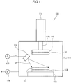
Fig. 1 is a diagram illustrating a schematic configuration of a substrate bonding apparatus used for explaining and implementing a procedure of a first embodiment of a substrate bonding method according to the present invention. -
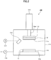
Fig. 2 is a diagram for explaining a procedure subsequent toFig. 1 . -
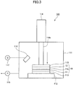
Fig. 3 is a diagram for explaining a procedure subsequent toFig. 2 . -
Fig. 4 is a diagram for explaining a procedure subsequent toFig. 3 . -
Fig. 5 is a diagram illustrating a schematic configuration of a substrate bonding apparatus used for explaining and implementing a procedure of a second embodiment of a substrate bonding method according to the present invention. -
Fig. 6 is a diagram for explaining a procedure subsequent toFig. 5 . -
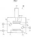
Fig. 7 is a diagram for explaining a procedure subsequent toFig. 6 . -
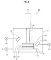
Fig. 8 is a diagram for explaining a procedure subsequent toFig. 7 . -
Fig. 9 is a diagram for explaining a procedure subsequent toFig. 8 . -
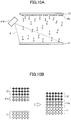
Fig. 10A is a diagram for explaining the action inFig. 1 andFig. 6 . -
Fig. 10B is a diagram for explaining the action inFig. 3 andFig. 8 . - Embodiments of substrate bonding methods according to the present invention will be described based on the drawings; however, the present invention is not limited only to the following embodiments described based on the drawings.
- A first embodiment of a substrate bonding method according to the present invention will be described based on
Figs. 1 to 4 . - As illustrated in
Fig. 1 , at a lower center portion inside achamber 111 is placed asupport base 112. On thesupport base 112, alower stage 113 is arranged so as to attachably and detachably hold afirst substrate 11 on its upper surface. To the upper center portion of the ceiling of thechamber 111 is attached the distal end of alifting cylinder 114 with its axial direction oriented in the up-down direction. The liftingcylinder 114 is configured to move the distal end of arod 114a upward and downward inside thechamber 111. To the lower surface of the distal end of therod 114a of thelifting cylinder 114 is attached anupper stage 115, which attachably and detachably holds asecond substrate 12 under its lower surface. - To the
chamber 111 is connected anexhaust pump 116 which evacuates thechamber 111 to make the inside a high vacuum environment. Inside thechamber 111 is arranged anion gun 118, such as a FAB, to be oriented with its delivery port directed to a surface (upper surface) of thefirst substrate 11 held on thelower stage 113. Theion gun 118 is connected to agas source 117 which supplies theion gun 118 withgas 1, such as argon, as feedstock gas. - The
first substrate 11 is made of at least one of a semiconductor material such as Si and Ge; a compound semiconductor material including a Ga based material such as GaN, GaAs, and GaP, and an In based material such as InP and InSb; and a metal material such as Au, Cu, and Al. On the other hand, thesecond substrate 12 is made of at least one of an amorphous oxide material such as amorphous SiO2; an amorphous nitride material such as amorphous SiN; an amorphous carbide material such as amorphous SiC, and an amorphous fluoride material such as amorphous CaF2. - Next, description will be provided for a substrate bonding method using the
substrate bonding apparatus 100 according to this embodiment described above. - First, the
first substrate 11 is attached to thelower stage 113, and thesecond substrate 12 is attached to the upper stage 115 (a substrate holding step) . Then, theexhaust pump 116 is operated to evacuate thechamber 111 to make the inside a high vacuum environment (an exhaust step). - Next, when the
gas 1 is supplied for theion gun 118 from thegas source 117 and theion gun 118 is turned on, theion gun 118 radiates abeam 2 of ion particles of thegas 1 toward the surface (upper surface) of thefirst substrate 11 on the lower stage 113 (seeFig. 1 ) . - With this operation, the surface (upper surface) of the
first substrate 11 made of a material described above is sputter-etched to be activated, and at the same time, sputtered particles Ms of a foregoing material of thefirst substrate 11 are attached to the surface (lower surface) of the second substrate 12 (seeFig. 10 A) . Thus, anactive layer 11a composed of the sputtered particles Ms of the foregoing material is formed so as to adhere to the surface (lower surface) of the second substrate 12 (seeFig. 2 ) (an activation step). - After the
active layer 11a composed of the sputtered particles Ms of the material of thefirst substrate 11 is formed so to adhere to the surface (lower surface) of thesecond substrate 12 in this way, the operation of theion gun 118 is stopped. Then, thelifting cylinder 114 is operated to extend therod 114a and lower theupper stage 115, so that thelower stage 113 and theupper stage 115 are brought relatively close to each other in the opposing direction. Theactive layer 11a of the surface (lower surface) of thesecond substrate 12 held by theupper stage 115 is pressed against the activated surface (upper surface) of thefirst substrate 11 held by thelower stage 113 with these surfaces in contact with each other (seeFig. 3 ) . Thus, thefirst substrate 11 and thesecond substrate 12 are bonded to each other via theactive layer 11a (seeFig. 10B ) (a bonding step). - After the surface (upper surface) of the
first substrate 11 is bonded to the surface (lower surface) of thesecond substrate 12 via theactive layer 11a as described above, theupper stage 115 releases the holding of thesecond substrate 12. Then, thelifting cylinder 114 is operated to shorten therod 114a to move theupper stage 115 upward, so that thelower stage 113 and theupper stage 115 relatively move apart from each other in the opposing direction. Thus, theupper stage 115 is disengaged from the second substrate 12 (seeFig. 4 ). - The operation of the
exhaust pump 116 is stopped, and the pressure inside thechamber 111 is returned to the atmospheric pressure. Then, thelower stage 113 releases the holding of thefirst substrate 11. Abonded material 10 is obtained by taking it out from the position on thelower stage 113 to the outside of thechamber 111. - In summary, as described earlier, the
beam 2 is radiated to thefirst substrate 11 made of the foregoing material to activate the surface of thefirst substrate 11 and also deposit the sputtered particles Ms of thefirst substrate 11 on the surface of thesecond substrate 12. Thus, theactive layer 11a of the sputtered particles Ms is formed on the surface of thesecond substrate 12 made of a material the activity of which tends to decrease so as to adhere to it (the activation step). The activated surface of thefirst substrate 11 and theactive layer 11a are pressed and bonded to each other (the bonding step). With these steps, thefirst substrate 11 is bonded to thesecond substrate 12 made of a material the activity of which tends to decrease in this embodiment. - As a result, in this embodiment, the
second substrate 12 made of a material the activity of which tends to decrease can be bonded to thefirst substrate 11 at room temperature with high strength. - Thus, according to this embodiment, a bonded
material 10 with a sufficient joint strength can be produced at room temperature using thesecond substrate 12 even made of a material the activity of which tends to decrease. - In addition, since radiating the
beam 2 to thefirst substrate 11 activates the surface of thefirst substrate 11 and also attaches the sputtered particles Ms that occur from thefirst substrate 11 to the surface of thesecond substrate 12 so that theactive layer 11a is formed so as to adhere to the surface of thesecond substrate 12, this eliminates the need for the dedicated material and process to form theactive layer 11a and suppresses the increase in cost and time to produce the bondedmaterial 10. - Here, Table 1 shows results of experiments conducted to confirm effects of the substrate bonding method according to this embodiment. Note that Table 1 also shows results of a conventional method which was conducted for comparison.
[Table 1] This embodiment Conventional method First substrate Si Si Second substrate Amorphous SiO2 Amorphous SiO2 Gas Ar Ar Beam radiation To only the first substrate for 2.5 minutes To both the first and second substrates for 2.5 minutes Surface energy (J/mm2) 1.3 0.3 - As can be seen from the above Table 1, the surface energy of the bonded surface between the first substrate and the second substrate by the conventional method was only 0.3 J/m2. On the other hand, it was confirmed that the surface energy in this embodiment was as much as 1.3 J/m2, which is a practical value (1.0 J/m2 or more).
- A second embodiment of a substrate bonding method according to the present invention will be described based on
Figs. 5 to 9 . Here, for the same parts as in the foregoing embodiment, the same reference signs as have been used in the description for the foregoing embodiment are used to omit explanation overlapped with the description for the foregoing embodiment. - As illustrated in
Fig. 5 , inside thechamber 111 is arranged anion gun 218, such as a FAB, to be oriented with its delivery port directed to the surface (lower surface) of thesecond substrate 12 held by theupper stage 115. Theion gun 218 is connected to agas source 217 which supplies theion gun 218 withgas 1, such as argon. - Specifically, although in the foregoing embodiment, the
ion gun 118 or other parts are arranged such that thebeam 2 can be radiated to only thefirst substrate 11 held by thelower stage 113; in this embodiment, theion gun 218 and other parts are also arranged such that thebeam 2 can be radiated to thesecond substrate 12 held by theupper stage 115. - Next, description will be provided for a substrate bonding method using the
substrate bonding apparatus 200 according to the embodiment described above. - First, as in the foregoing embodiment, a
first substrate 11 is attached to thelower stage 113, and also asecond substrate 12 is attached to the upper stage 115 (the substrate holding step). Then, theexhaust pump 116 is turned on to evacuate thechamber 111 and make the inside a high vacuum environment (the exhaust step). - Next, when the
gas 1 is supplied to theion gun 218 from thegas source 217, and theion gun 218 is turned on, theion gun 218 radiates abeam 2 of ion particles of thegas 1 toward the surface (lower surface) of thesecond substrate 12 under the upper stage 115 (seeFig. 5 ). With this operation, the surface (lower surface) of thesecond substrate 12 is sputter-etched and cleaned (a cleaning step). - After the surface (lower surface) of the
second substrate 12 is cleaned in this way, the operation of theion gun 218 is stopped. Then, as in the foregoing embodiment, thegas source 117 supplies thegas 1 to theion gun 118, and theion gun 118 is turned on, so that theion gun 118 radiates thebeam 2 of ion particles of thegas 1 toward the surface (upper surface) of thefirst substrate 11 on the lower stage 113 (seeFig. 6 ). As in the foregoing embodiment, the surface of the first substrate 11 (upper surface) is sputter-etched and activated, and at the same time, the sputtered particles Ms of thefirst substrate 11 are deposited on the surface (lower surface) of the second substrate 12 (seeFig. 10A ). With this operation, anactive layer 11a composed of the sputtered particles Ms is formed on the surface (lower surface) of thesecond substrate 12 so as to adhere to it (seeFig. 7 ) (the activation step). - Next, as in the foregoing embodiment, after the operation of the
ion gun 118 is stopped, thelifting cylinder 114 is operated so that thelower stage 113 and theupper stage 115 are brought relatively close to each other in the opposing direction. Then, theactive layer 11a of the surface (lower surface) of thesecond substrate 12 held by theupper stage 115 is pressed against the activated surface (upper surface) of thefirst substrate 11 held by thelower stage 113 with these surfaces in contact with each other (seeFig. 8 ). Thus, thefirst substrate 11 and thesecond substrate 12 are bonded to each other via theactive layer 11a (seeFig. 10B ) (the bonding step). - Next, as in the foregoing embodiment, the
upper stage 115 releases the holding of thesecond substrate 12. Then, thelifting cylinder 114 is operated to move theupper stage 115 upward, so that thelower stage 113 and theupper stage 115 relatively move apart from each other in the opposing direction (seeFig. 9 ) . After that, the operation of theexhaust pump 116 is stopped, and the pressure inside thechamber 111 is returned to the atmospheric pressure. Then, thelower stage 113 releases the holding of thefirst substrate 11. A bondedmaterial 10 is taken out from the position on thelower stage 113 to the outside of thechamber 111. - In summary, in this embodiment, the surface of the
second substrate 12 is cleaned in advance by irradiating thesecond substrate 12 with thebeam 2 and sputter-etching it, before the foregoing activation step in the foregoing embodiment is performed. - As result, in this embodiment, the adhesion of the
active layer 11a to the surface (lower surface) of thesecond substrate 12 can be further increased, compared to the case in the foregoing embodiment. - Thus, this embodiment not only provides the same effect as in the foregoing embodiment as a matter of course but also provides a bonded
material 10 with a bonding strength higher than the cases in the foregoing embodiment. - Note that in the activation step, in order to form an
active layer 11a with a necessary and sufficient thickness (about 0.5 nm) on the surface of thesecond substrate 12 with the sputtered particles Ms from thefirst substrate 11, thefirst substrate 11 is irradiated with thebeam 2 for necessary and sufficient time (for example, about 1 minute) . On the other hand, in the cleaning step, thesecond substrate 12 is irradiated with thebeam 2 for necessary and sufficient time (for example, about 30 seconds) to remove contamination such as natural oxide film formed on the surface of thesecond substrate 12. Accordingly, this cleaning step does not activate the surface of thesecond substrate 12, unlike the activation step. - In addition, it is preferable that the distance between the
first substrate 11 and thesecond substrate 12 in the opposing direction be large in the cleaning step so that the contamination such as natural oxide film removed from the surface of thesecond substrate 12 is less likely to be attached to the surface of thefirst substrate 11. In contrast, it is preferable that the distance between thefirst substrate 11 and thesecond substrate 12 in the opposing direction be small in the activation step to the extent where the radiation of thebeam 2 to thefirst substrate 11 is not hindered so that the sputtered particles Ms from thefirst substrate 11 can be deposited on the surface of thesecond substrate 12 efficiently. - Note that although in the foregoing first embodiment, the
lower stage 113 holds thefirst substrate 11, while theupper stage 115 holds thesecond substrate 12, and theion gun 118 is arranged such that the delivery port is directed to thefirst substrate 11 held by thelower stage 113; in another embodiment, the same effect as in the foregoing first embodiment can be obtained, for example, with the configuration in which theupper stage 115 holds thefirst substrate 11, while thelower stage 113 holds thesecond substrate 12, and the ion gun is arranged such that the delivery port is directed to thefirst substrate 11 held by theupper stage 115. - In addition, although the foregoing second embodiment includes two ion guns, the
ion gun 118 oriented such that the delivery port is directed to thefirst substrate 11 held by thelower stage 113 and theion gun 218 oriented such that the delivery port is directed to thesecond substrate 12 held by theupper stage 115; in another embodiment, the same effect as in the foregoing second embodiment can be obtained, for example, with the configuration including a single ion gun capable of changing the direction of the delivery port between to thefirst substrate 11 held by thelower stage 113 and to thesecond substrate 12 held by theupper stage 115. - In addition, although in the foregoing second embodiment, the
lower stage 113 holds thefirst substrate 11, while theupper stage 115 holds thesecond substrate 12; in another embodiment, the same effect as in the foregoing second embodiment can be obtained, for example, with the configuration in which theupper stage 115 holds thefirst substrate 11, and thelower stage 113 holds thesecond substrate 12. - In addition, the foregoing embodiments have the configuration in which the
lower stage 113 is arranged on the floor side of thechamber 111 via thesupport base 112, while theupper stage 115 is arranged on the ceiling side of thechamber 111 via thelifting cylinder 114, and thelower stage 113 and theupper stage 115 can be moved relatively close to or apart from each other in the opposing direction by the operation of thelifting cylinder 114. However, another embodiment can employ, for example, a configuration in which thelower stage 113 is arranged on the floor side of thechamber 111 via moving means capable of lifting up and down thelower stage 113, while theupper stage 115 is arranged on the ceiling side of thechamber 111 via a support member, and thelower stage 113 and theupper stage 115 can move relatively close to or apart from each other in the opposing direction by operating the moving means . Alternatively, another embodiment can employ, for example, a configuration in which thelower stage 113 is arranged on the floor side of thechamber 111 via first moving means capable of lifting up and down thelower stage 113, while theupper stage 115 is arranged on the ceiling side of thechamber 111 via second moving means capable of lifting up and down theupper stage 115, and thelower stage 113 and theupper stage 115 can move relatively close to or apart from each other in the opposing direction by operating the first and second moving means. - In addition, although in the foregoing embodiments, description has been provided for the cases where the
second substrate 12 is made of at least one of an amorphous oxide material such as amorphous SiO2, an amorphous nitride material such as amorphous SiN, an amorphous carbide material such as amorphous SiC, and an amorphous fluoride material such as amorphous CaF2, the present invention is not limited to these materials. For example, the second substrate can be used in the same way as in the foregoing embodiments if the second substrate is made of at least one of materials including a crystalline oxide material such as crystalline SiO2, a crystalline nitride material such as crystalline SiN, a crystalline carbide materials such as crystalline SiC, and a crystalline fluoride material such as crystalline CaF2, and further including, in the same way as for thefirst substrate 11, a semiconductor material such as Si and Ge, a compound semiconductor material including a Ga based material such as GaN, GaAs, and GaP and an In based material such as InP and InSb, and a metal material such as Au, Cu, and Al. - However, it is much preferable that the
second substrate 12 be made of at least one of an amorphous oxide material such as amorphous SiO2, an amorphous nitride material such as amorphous SiN, an amorphous carbide material such as amorphous SiC, and an amorphous fluoride material such as amorphous CaF2 as in the foregoing embodiments, because the substrate bonding method according to the present invention can utilized most effectively in these cases. - The substrate bonding method according to the present invention can be utilized very usefully from the industrial point of view because the second substrate can be bonded to the first substrate at room temperature with a high strength, for example, even if the second substrate is made of a material the activity of which tends to decrease.
-
- 1
- gas
- 2
- beam
- 10
- bonded material
- 11
- first substrate
- 11a
- active layer
- 12
- second substrate
- 100, 200
- substrate bonding apparatus
- 111
- chamber
- 112
- support base
- 113
- lower stage
- 114
- lifting cylinder
- 114a
- rod
- 115
- upper stage
- 116
- exhaust pump
- 117, 217
- gas source
- 118, 218
- ion gun
Claims (3)
- A substrate bonding method of bonding a first substrate and a second substrate by sputter-etching, characterized in that
the first substrate is made of at least one of a semiconductor material, a compound semiconductor material, and a metal material, and
the substrate bonding method comprises:an activation step of sputter-etching a surface of the first substrate by irradiating the surface of the first substrate with a beam of ion particles, to deposit sputtered particles of the first substrate on a surface of the second substrate; anda bonding step of bonding the second substrate and the first substrate by bringing the surface of the second substrate on which the sputtered particles of the first substrate have been deposited and the surface of the first substrate that have been sputter-etched into contact with each other. - The substrate bonding method according to claim 1, characterized in that
the substrate bonding method further comprises, before the activation step, a cleaning step of sputter-etching the surface of the second substrate by irradiating the surface of the second substrate with a beam of ion particles to clean the surface of the second substrate. - The substrate bonding method according to claim 1 or 2, characterized in that
the second substrate is made of at least one of an oxide material, a nitride material, a carbide material, a fluoride material, a semiconductor material, a compound semiconductor material, and a metal material.
Applications Claiming Priority (2)
| Application Number | Priority Date | Filing Date | Title |
|---|---|---|---|
| JP2016149295A JP6344622B2 (en) | 2016-07-29 | 2016-07-29 | Substrate bonding method |
| PCT/JP2017/018186 WO2018020780A1 (en) | 2016-07-29 | 2017-05-15 | Substrate joining method |
Publications (2)
| Publication Number | Publication Date |
|---|---|
| EP3493242A1 true EP3493242A1 (en) | 2019-06-05 |
| EP3493242A4 EP3493242A4 (en) | 2020-01-01 |
Family
ID=61017140
Family Applications (1)
| Application Number | Title | Priority Date | Filing Date |
|---|---|---|---|
| EP17833791.1A Withdrawn EP3493242A4 (en) | 2016-07-29 | 2017-05-15 | SUBSTRATE JOINING METHOD |
Country Status (5)
| Country | Link |
|---|---|
| US (1) | US20190172813A1 (en) |
| EP (1) | EP3493242A4 (en) |
| JP (1) | JP6344622B2 (en) |
| CN (1) | CN109690731A (en) |
| WO (1) | WO2018020780A1 (en) |
Cited By (1)
| Publication number | Priority date | Publication date | Assignee | Title |
|---|---|---|---|---|
| US11450643B2 (en) | 2019-09-05 | 2022-09-20 | Tohoku University | Chemical bonding method and joined structure |
Families Citing this family (3)
| Publication number | Priority date | Publication date | Assignee | Title |
|---|---|---|---|---|
| JP7024668B2 (en) | 2018-09-05 | 2022-02-24 | 株式会社Sumco | SOI wafer and its manufacturing method |
| JP7131778B2 (en) * | 2019-09-05 | 2022-09-06 | 国立大学法人東北大学 | Chemical bonding method and joint structure |
| JP7584721B1 (en) * | 2024-03-29 | 2024-11-15 | 日本碍子株式会社 | Composite Board |
Family Cites Families (12)
| Publication number | Priority date | Publication date | Assignee | Title |
|---|---|---|---|---|
| JP2791429B2 (en) * | 1996-09-18 | 1998-08-27 | 工業技術院長 | Room-temperature bonding of silicon wafers |
| JP2004273941A (en) * | 2003-03-11 | 2004-09-30 | Toray Eng Co Ltd | Joining method and apparatus |
| JP3970304B1 (en) * | 2006-03-27 | 2007-09-05 | 三菱重工業株式会社 | Room temperature bonding equipment |
| JP4172806B2 (en) * | 2006-09-06 | 2008-10-29 | 三菱重工業株式会社 | Room temperature bonding method and room temperature bonding apparatus |
| JP4889562B2 (en) * | 2007-05-14 | 2012-03-07 | パナソニック株式会社 | Joining apparatus and joining method |
| JP2010275423A (en) * | 2009-05-28 | 2010-12-09 | Seiko Epson Corp | Joining method and joined body |
| CN103460339B (en) * | 2011-01-31 | 2017-05-31 | 须贺唯知 | Composition surface preparation method, engagement substrate, substrate bonding method, composition surface producing device and substrate conjugant |
| JP5658135B2 (en) * | 2011-12-28 | 2015-01-21 | 住友ゴム工業株式会社 | Method for producing composite of surface-modified fluororesin film and thermoplastic resin |
| JP6205557B2 (en) * | 2012-01-13 | 2017-10-04 | ボンドテック株式会社 | Bonding apparatus, bonding method, semiconductor device manufacturing method, and MEMS device manufacturing method |
| JP6037734B2 (en) * | 2012-09-07 | 2016-12-07 | 三菱重工工作機械株式会社 | Room temperature bonding apparatus and room temperature bonding method |
| JP2014107393A (en) * | 2012-11-27 | 2014-06-09 | Mitsubishi Heavy Ind Ltd | Normal temperature bonding device, wafer having normal temperature bonding device and normal temperature bonding method |
| JP6164770B2 (en) * | 2013-05-09 | 2017-07-19 | 須賀 唯知 | Substrate surface treatment method and apparatus |
-
2016
- 2016-07-29 JP JP2016149295A patent/JP6344622B2/en active Active
-
2017
- 2017-05-15 CN CN201780045920.7A patent/CN109690731A/en active Pending
- 2017-05-15 WO PCT/JP2017/018186 patent/WO2018020780A1/en not_active Ceased
- 2017-05-15 US US16/321,282 patent/US20190172813A1/en not_active Abandoned
- 2017-05-15 EP EP17833791.1A patent/EP3493242A4/en not_active Withdrawn
Cited By (2)
| Publication number | Priority date | Publication date | Assignee | Title |
|---|---|---|---|---|
| US11450643B2 (en) | 2019-09-05 | 2022-09-20 | Tohoku University | Chemical bonding method and joined structure |
| US12451461B2 (en) | 2019-09-05 | 2025-10-21 | Tohoku University | Chemical bonding method and joined structure |
Also Published As
| Publication number | Publication date |
|---|---|
| EP3493242A4 (en) | 2020-01-01 |
| WO2018020780A1 (en) | 2018-02-01 |
| JP6344622B2 (en) | 2018-06-20 |
| US20190172813A1 (en) | 2019-06-06 |
| JP2018018996A (en) | 2018-02-01 |
| CN109690731A (en) | 2019-04-26 |
Similar Documents
| Publication | Publication Date | Title |
|---|---|---|
| US10164144B2 (en) | Bond and release layer transfer process | |
| US20190024259A1 (en) | Techniques for forming optoelectronic devices | |
| US10186630B2 (en) | Seed wafer for GaN thickening using gas- or liquid-phase epitaxy | |
| JP6396852B2 (en) | Method for manufacturing composite wafer having oxide single crystal thin film | |
| US20190172813A1 (en) | Substrate joining method | |
| JP2023054158A (en) | Joining system and joining method | |
| TW201222623A (en) | Securing mechanism and method for wafer bonder | |
| JP7512641B2 (en) | Method for manufacturing bonded substrate | |
| JP2008283086A (en) | Joining apparatus and joining method | |
| WO2022158520A1 (en) | Joining method, joining device and joining system | |
| WO2018020781A1 (en) | Substrate joining device and substrate joining method using same | |
| JP7476720B2 (en) | Substrate bonding apparatus and method for manufacturing bonded substrate | |
| CN106129220A (en) | The manufacture method of a kind of LED chip and making apparatus thereof | |
| JP7512761B2 (en) | Substrate Bonding Equipment | |
| WO2022158563A1 (en) | Joining method, joining device, and joining system | |
| JP2018532258A (en) | Epitaxial growth using a preparation process with atmospheric pressure plasma | |
| JP7540813B1 (en) | Bonding method, bonding system, irradiation device, and activation treatment device | |
| Suga et al. | Feasibility of SAB using nano-adhesion layer for low temperature GaN wafer bonding | |
| Rogers et al. | Wafer bonding tool including dual plasma capability for in-situ sputter etching prior to aligned bonding | |
| JP2013115307A (en) | Method for manufacturing group iii nitride composite substrate |
Legal Events
| Date | Code | Title | Description |
|---|---|---|---|
| STAA | Information on the status of an ep patent application or granted ep patent |
Free format text: STATUS: THE INTERNATIONAL PUBLICATION HAS BEEN MADE |
|
| PUAI | Public reference made under article 153(3) epc to a published international application that has entered the european phase |
Free format text: ORIGINAL CODE: 0009012 |
|
| STAA | Information on the status of an ep patent application or granted ep patent |
Free format text: STATUS: REQUEST FOR EXAMINATION WAS MADE |
|
| 17P | Request for examination filed |
Effective date: 20190129 |
|
| AK | Designated contracting states |
Kind code of ref document: A1 Designated state(s): AL AT BE BG CH CY CZ DE DK EE ES FI FR GB GR HR HU IE IS IT LI LT LU LV MC MK MT NL NO PL PT RO RS SE SI SK SM TR |
|
| AX | Request for extension of the european patent |
Extension state: BA ME |
|
| RAP1 | Party data changed (applicant data changed or rights of an application transferred) |
Owner name: NATIONAL INSTITUTE OF ADVANCED INDUSTRIAL SCIENCE Owner name: MITSUBISHI HEAVY INDUSTRIES MACHINE TOOL CO., LTD. |
|
| DAV | Request for validation of the european patent (deleted) | ||
| DAX | Request for extension of the european patent (deleted) | ||
| A4 | Supplementary search report drawn up and despatched |
Effective date: 20191203 |
|
| RIC1 | Information provided on ipc code assigned before grant |
Ipc: H01L 21/3065 20060101ALI20191127BHEP Ipc: H01L 21/20 20060101ALI20191127BHEP Ipc: H01L 21/02 20060101AFI20191127BHEP Ipc: H01L 21/302 20060101ALI20191127BHEP Ipc: B23K 20/24 20060101ALI20191127BHEP Ipc: B23K 20/00 20060101ALI20191127BHEP |
|
| STAA | Information on the status of an ep patent application or granted ep patent |
Free format text: STATUS: EXAMINATION IS IN PROGRESS |
|
| 17Q | First examination report despatched |
Effective date: 20211220 |
|
| STAA | Information on the status of an ep patent application or granted ep patent |
Free format text: STATUS: THE APPLICATION HAS BEEN WITHDRAWN |
|
| 18W | Application withdrawn |
Effective date: 20220421 |