EP3492940A1 - Display device capable of performing self-diagnosis in relation to partial discharge - Google Patents
Display device capable of performing self-diagnosis in relation to partial discharge Download PDFInfo
- Publication number
- EP3492940A1 EP3492940A1 EP18194136.0A EP18194136A EP3492940A1 EP 3492940 A1 EP3492940 A1 EP 3492940A1 EP 18194136 A EP18194136 A EP 18194136A EP 3492940 A1 EP3492940 A1 EP 3492940A1
- Authority
- EP
- European Patent Office
- Prior art keywords
- partial discharge
- display device
- group
- controller
- parameters
- Prior art date
- Legal status (The legal status is an assumption and is not a legal conclusion. Google has not performed a legal analysis and makes no representation as to the accuracy of the status listed.)
- Granted
Links
Images

Classifications
-
- G—PHYSICS
- G06—COMPUTING OR CALCULATING; COUNTING
- G06F—ELECTRIC DIGITAL DATA PROCESSING
- G06F11/00—Error detection; Error correction; Monitoring
- G06F11/07—Responding to the occurrence of a fault, e.g. fault tolerance
- G06F11/0703—Error or fault processing not based on redundancy, i.e. by taking additional measures to deal with the error or fault not making use of redundancy in operation, in hardware, or in data representation
-
- G—PHYSICS
- G01—MEASURING; TESTING
- G01R—MEASURING ELECTRIC VARIABLES; MEASURING MAGNETIC VARIABLES
- G01R31/00—Arrangements for testing electric properties; Arrangements for locating electric faults; Arrangements for electrical testing characterised by what is being tested not provided for elsewhere
- G01R31/12—Testing dielectric strength or breakdown voltage ; Testing or monitoring effectiveness or level of insulation, e.g. of a cable or of an apparatus, for example using partial discharge measurements; Electrostatic testing
-
- G—PHYSICS
- G01—MEASURING; TESTING
- G01R—MEASURING ELECTRIC VARIABLES; MEASURING MAGNETIC VARIABLES
- G01R31/00—Arrangements for testing electric properties; Arrangements for locating electric faults; Arrangements for electrical testing characterised by what is being tested not provided for elsewhere
- G01R31/26—Testing of individual semiconductor devices
- G01R31/2607—Circuits therefor
- G01R31/2632—Circuits therefor for testing diodes
- G01R31/2635—Testing light-emitting diodes, laser diodes or photodiodes
-
- G—PHYSICS
- G01—MEASURING; TESTING
- G01R—MEASURING ELECTRIC VARIABLES; MEASURING MAGNETIC VARIABLES
- G01R31/00—Arrangements for testing electric properties; Arrangements for locating electric faults; Arrangements for electrical testing characterised by what is being tested not provided for elsewhere
- G01R31/44—Testing lamps
-
- G—PHYSICS
- G02—OPTICS
- G02F—OPTICAL DEVICES OR ARRANGEMENTS FOR THE CONTROL OF LIGHT BY MODIFICATION OF THE OPTICAL PROPERTIES OF THE MEDIA OF THE ELEMENTS INVOLVED THEREIN; NON-LINEAR OPTICS; FREQUENCY-CHANGING OF LIGHT; OPTICAL LOGIC ELEMENTS; OPTICAL ANALOGUE/DIGITAL CONVERTERS
- G02F1/00—Devices or arrangements for the control of the intensity, colour, phase, polarisation or direction of light arriving from an independent light source, e.g. switching, gating or modulating; Non-linear optics
- G02F1/01—Devices or arrangements for the control of the intensity, colour, phase, polarisation or direction of light arriving from an independent light source, e.g. switching, gating or modulating; Non-linear optics for the control of the intensity, phase, polarisation or colour
- G02F1/13—Devices or arrangements for the control of the intensity, colour, phase, polarisation or direction of light arriving from an independent light source, e.g. switching, gating or modulating; Non-linear optics for the control of the intensity, phase, polarisation or colour based on liquid crystals, e.g. single liquid crystal display cells
- G02F1/1306—Details
- G02F1/1309—Repairing; Testing
-
- G—PHYSICS
- G06—COMPUTING OR CALCULATING; COUNTING
- G06F—ELECTRIC DIGITAL DATA PROCESSING
- G06F11/00—Error detection; Error correction; Monitoring
- G06F11/07—Responding to the occurrence of a fault, e.g. fault tolerance
- G06F11/0703—Error or fault processing not based on redundancy, i.e. by taking additional measures to deal with the error or fault not making use of redundancy in operation, in hardware, or in data representation
- G06F11/0751—Error or fault detection not based on redundancy
-
- G—PHYSICS
- G06—COMPUTING OR CALCULATING; COUNTING
- G06F—ELECTRIC DIGITAL DATA PROCESSING
- G06F11/00—Error detection; Error correction; Monitoring
- G06F11/07—Responding to the occurrence of a fault, e.g. fault tolerance
- G06F11/0703—Error or fault processing not based on redundancy, i.e. by taking additional measures to deal with the error or fault not making use of redundancy in operation, in hardware, or in data representation
- G06F11/0766—Error or fault reporting or storing
-
- G—PHYSICS
- G06—COMPUTING OR CALCULATING; COUNTING
- G06F—ELECTRIC DIGITAL DATA PROCESSING
- G06F11/00—Error detection; Error correction; Monitoring
- G06F11/07—Responding to the occurrence of a fault, e.g. fault tolerance
- G06F11/0703—Error or fault processing not based on redundancy, i.e. by taking additional measures to deal with the error or fault not making use of redundancy in operation, in hardware, or in data representation
- G06F11/079—Root cause analysis, i.e. error or fault diagnosis
-
- G—PHYSICS
- G06—COMPUTING OR CALCULATING; COUNTING
- G06F—ELECTRIC DIGITAL DATA PROCESSING
- G06F3/00—Input arrangements for transferring data to be processed into a form capable of being handled by the computer; Output arrangements for transferring data from processing unit to output unit, e.g. interface arrangements
- G06F3/14—Digital output to display device ; Cooperation and interconnection of the display device with other functional units
- G06F3/1415—Digital output to display device ; Cooperation and interconnection of the display device with other functional units with means for detecting differences between the image stored in the host and the images displayed on the displays
-
- G—PHYSICS
- G09—EDUCATION; CRYPTOGRAPHY; DISPLAY; ADVERTISING; SEALS
- G09G—ARRANGEMENTS OR CIRCUITS FOR CONTROL OF INDICATING DEVICES USING STATIC MEANS TO PRESENT VARIABLE INFORMATION
- G09G3/00—Control arrangements or circuits, of interest only in connection with visual indicators other than cathode-ray tubes
- G09G3/006—Electronic inspection or testing of displays and display drivers, e.g. of LED or LCD displays
-
- G—PHYSICS
- G09—EDUCATION; CRYPTOGRAPHY; DISPLAY; ADVERTISING; SEALS
- G09G—ARRANGEMENTS OR CIRCUITS FOR CONTROL OF INDICATING DEVICES USING STATIC MEANS TO PRESENT VARIABLE INFORMATION
- G09G2320/00—Control of display operating conditions
- G09G2320/04—Maintaining the quality of display appearance
- G09G2320/043—Preventing or counteracting the effects of ageing
-
- G—PHYSICS
- G09—EDUCATION; CRYPTOGRAPHY; DISPLAY; ADVERTISING; SEALS
- G09G—ARRANGEMENTS OR CIRCUITS FOR CONTROL OF INDICATING DEVICES USING STATIC MEANS TO PRESENT VARIABLE INFORMATION
- G09G2330/00—Aspects of power supply; Aspects of display protection and defect management
- G09G2330/04—Display protection
Definitions
- the present disclosure relates to a display device capable of performing a self-diagnosis in relation to a partial discharge.
- a partial discharge may occur in a display device. That is, when a high electric field is concentrated on a particular portion of the display device, the partial discharge may occur at the particular portion of the display device on which the high electric field is concentrated.
- the partial discharge may include at least one among a corona discharge, a surface discharge, and a void discharge.
- the display device may be deteriorated due to the partial discharge.
- a dielectric breakdown may occur in the display device.
- the dielectric breakdown may be a cause of malfunction of display device.
- the present disclosure is directed to a display device capable of performing a self-diagnosis in relation to a partial discharge and preventing a malfunction thereof.
- a display device includes an image processor configured to process an image signal, and a display unit configured to display the processed image signal.
- the image processor may include a detector configured to determine a group of parameters by detecting a waveform of a detected partial discharge and measuring each of parameters of the waveform in the form of a binary number, and a controller configured to identify the detected partial discharge by comparing the determined group with previously stored groups.
- the controller may include an arithmetic unit configured to update the previously stored groups by performing an operation on at least one among the previously stored groups.
- the arithmetic unit may be further configured to perform at least one of a selection operation of selecting at least one first group from among the previously stored groups, a crossover operation of generating a second group by combining parameters of at least two groups among the previously stored groups, a mutation operation of generating a third group by changing at least one of parameters of the first or second group, and a substitution operation of replacing one of the previously stored groups with the first group, the second group, or the third group.
- the parameters may include at least one of a phase of the partial discharge, a magnitude of the partial discharge, a frequency of occurrence of the partial discharge, a maximum magnitude of the partial discharge, an average discharge amount, a firing voltage, and an extinction voltage.
- the image processor may further include a memory in which identification information of the partial discharge is mapped to each of the previously stored groups.
- the identification information may include at least one of a cause of the partial discharge, a location at which the partial discharge has occurred, and a degree of risk of the partial discharge.
- the controller may be further configured to diagnose a state of the display device on the basis of the identification information of the detected partial discharge.
- the controller may output an alarm message or power off the display device on the basis of the identification information of the detected partial discharge.
- the detector may include a first impedance element configured to decrease an output impedance when the partial discharge occurs, a first condenser in which a dielectric breakdown occurs when the output impedance of the first impedance element decreases, a second condenser of which an output voltage increases when the dielectric breakdown occurs in the first condenser, a second impedance element to which the increased output voltage of the second condenser is applied, and a sensing element configured to sense the occurring partial discharge on the basis of a voltage input from the second impedance element.
- the image processor may further include a converter configured to output the image signal in the form of digital data to the display unit.
- the detector may detect a partial discharge occurring in the converter.
- the terms such as “include”, “may include”, “comprise”, and “may comprise” specify the presence of stated features, values, functions, and elements, e.g., components, but do not preclude the presence or addition of one or more other features, values, functions, and elements.
- first or second may be used herein to describe various elements regardless of an order and/or importance, and these elements should not be limited by these terms. These terms are only used to distinguish one element from another element.
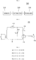
- FIG. 1 is a block diagram illustrating an internal structure of a display device 100 according to an embodiment of the present disclosure.
- the display device 100 may display an image signal received from an external device (not shown).
- the display device 100 may be connected to the external device via wire or wirelessly.
- the display device 100 may interface with the external device and receive the image signal from the external device.
- the external device may include a circuit breaker, and the display device 100 may be a liquid crystal display (LCD) device. That is, the display device 100 may include a display unit 120 and an image processor 110.
- LCD liquid crystal display
- the display unit 120 may display the image signal.
- the display unit 120 may include an LCD panel.
- the image processor 110 may control overall operations of the display device 100.
- the image processor 110 may control the display unit 120.
- the image processor 110 may output the image signal received from the external device to the display unit 120.
- the image processor 110 may process the image signal according to features and a size of the display unit 120.
- the image processor 110 may identify a partial discharge occurring therein and perform a self-diagnosis. In this case, the image processor 110 may control the display device 100 in response to the partial discharge.
- FIG. 2 is a block diagram illustrating an internal structure of the image processor 110 according to an embodiment of the present disclosure.
- FIG. 3 is a block diagram of a detector of FIG. 2 .
- FIG. 4 is a circuit diagram of a sensor of FIG. 3.
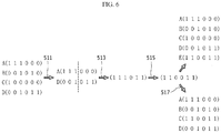
- FIGS. 5 and 6 are diagrams illustrating examples of a memory and a controller of FIG. 2 .
- an image processor 200 (or the image processor 110 of FIG. 1 according to an embodiment of the present disclosure may include a converter 210, a detector 220, a controller 230, and a memory 240.
- the converter 210 may convert an image signal according to features and a size of the display unit 120 of FIG. 1 . Furthermore, the converter 210 may output the image signal to the display unit 120. In this case, the converter 210 may output the image signal in the form of digital data. To this end, the converter 210 may be formed by mounting a plurality of components on a substrate.
- the converter 210 may include an image decoder, an analog-digital converter (ADC), a scaler, and a power supply.
- ADC analog-digital converter
- the image decoder may decode the image signal.
- the ADC may receive a synchronization signal and an RGB signal corresponding to the image signal, and convert the RGB signal from an analog signal to digital data on the basis of the synchronization signal.
- the scaler may scale the image signal and the RGB signal and output the scaled image signal and RGB signal to the display unit 120.
- the power supply may supply power to the display unit 120.
- a partial discharge may occur in the converter 210. That is, when a high electric field is concentrated at a particular portion of the converter 210, the partial discharge may occur at the particular portion of the converter 210 on which the high electric field is concentrated. In this case, the partial discharge may occur at various locations and due to various causes.
- the partial discharge may include at least one among a corona discharge, a surface discharge, and a void discharge.
- the particular portion of the converter 210 at which the partial discharge occurs may deteriorate.
- a dielectric breakdown may occur in the converter 210.
- the dielectric breakdown may be a cause of malfunction of the display device 100.
- the detector 220 may detect the partial discharge occurring in the converter 210 by detecting a waveform of the partial discharge.
- the detector 220 may measure the waveform of the partial discharge in the form of data consisting of a plurality of bits.
- a detector 300 may include a sensor 310, an extractor 320, and a measurer 330.
- the sensor 310 may sense a partial discharge occurring in the converter 210.
- the sensor 310 may sense the partial discharge in response to an input signal from the converter 210.
- the sensor 310 may include a ceramic coupler.
- a sensor 400 may include a first impedance element 410, a first condenser 420, a second condenser 430, a second impedance element 440, and a sensing element 450.
- the first impedance element 410 may respond to a partial discharge. That is, when a partial discharge occurs in the converter 210, an output impedance of the first impedance element 410 may decrease.
- the first condenser 420 may be connected in series to the first impedance element 410. When the output impedance of the first impedance element 410 decreases, a dielectric breakdown may occur in the first condenser 420.
- the second condenser 430 may be connected in series to the first impedance element 410 and connected in parallel to the first condenser 420. When a dielectric breakdown occurs in the first condenser 420, an output voltage of the second condenser 430 may increase.
- the second impedance element 440 may be connected in series to the second condenser 430. That is, the output voltage of the second condenser 430 may be applied to the second impedance element 440.
- the sensing element 450 may be connected to the second impedance element 440.
- the sensing element 450 may sense the partial discharge on the basis of a voltage input from the second impedance element 440.
- the extractor 320 may extract a waveform of the partial discharge.
- the extractor 320 may extract the waveform of the partial discharge by removing a noise signal from an input signal.
- the extractor 320 may include a finite impulse response (FIR) filter.
- the measurer 330 may measure a predetermined number of parameters, e.g., N parameters, from the waveform of the partial discharge.
- the parameters may include at least one among a phase of the partial discharge, a magnitude of the partial discharge, a frequency of occurrence of the partial discharge, a maximum intensity of the partial discharge, an average discharge amount, a firing voltage, and an extinction voltage.
- the measurer 330 may determine a group of parameters on the basis of a genetic algorithm. That is, the measurer 330 may measure each of the parameters in the form of a binary number. Here, the measurer 330 may measure each of the parameters in the form of a bit and express each of the parameters as 0 or 1. For example, the measurer 330 may determine a bit corresponding to each of the parameters according to whether each of the parameters is greater than a predetermined threshold value. Furthermore, the measurer 330 may determine the group of the parameters by consecutively arranging the bits corresponding to the parameters in a predetermined order.
- the term "detection group" to be described below may be understood as a group determined by the measurer 330. For example, the detection group maybe expressed as (0 0 1 0 1 1).
- the memory 240 may store programs for operating the display device 100.
- the memory 240 may store a program for detecting a partial discharge occurring in the converter 210.
- the memory 240 may store data generated during execution of the programs.
- the memory 240 may store a plurality of groups each representing waveforms of partial discharges which may occur in the converter 210.
- the term "reference group" to be described below may be understood as a group stored in the memory 240.
- the memory 240 may store a plurality of reference groups A, B, C and D.
- each of the reference groups A, B, C and D may be formed based on the genetic algorithm. That is, each of the reference groups A, B, C and D may consist of bits determined to correspond to a predetermined number of parameters, e.g., N parameters, from one of waveforms.
- the bits may be consecutively arranged in the predetermined order.
- Each of the parameters may correspond to one of the bits expressed in the form of a binary number, i.e., 0 or 1.
- the memory 240 may store identification information identifying a partial discharge which may occur in the converter 210 to be mapped to one of the reference groups.
- the identification information may include at least one among a cause of the partial discharge, a location at which the partial discharge has occurred, and a degree of risk of the partial discharge.
- the degree of risk of the partial discharge may vary according to at least one among the cause of the partial discharge, the location on the converter 210 at which the partial discharge has occurred, and a frequency of occurrence of the partial discharge.
- the controller 230 may control overall operations of the display device 100 of FIG. 1 . Furthermore, the controller 230 may identify a partial discharge detected in the converter 210. To this end, the controller 230 may compare a detection group with the reference groups.
- the controller 230 may determine whether the detection group is identical to one of the reference groups. When the detection group is identical to one of the reference groups, the controller 230 may check identification information of the reference group identical to the detection group. Here, the controller 230 may update the identification information of the reference group identical to the detection group. For example, when the detection group is identical to the reference group B, the controller 230 may increase a degree of risk of the reference group B.
- the controller 230 may diagnose a state of the display device 100 in response to the partial discharge.
- the controller 230 may diagnose the state of the display device 100 on the basis of the identification information of the reference group identical to the detection group.
- the controller 230 may predict a degree of deterioration of the converter 210 by analyzing the identification information of the reference group identical to the detection group. For example, the controller 230 may predict the degree of deterioration of the converter 210 on the basis of at least one among the cause of the partial discharge, the location at which the partial discharge has occurred, and the degree of risk of the partial discharge.
- the controller 230 may diagnose the degree of deterioration of the converter 210 by comparing the degree of risk of the partial discharge with at least one predetermined threshold value.
- the controller 230 may output an alarm message to repair, inspect, or replace the converter 210.
- the controller 230 may transmit the alarm message to an external device or display the alarm message via the display unit 120.
- the controller 230 may power off the display device 100.
- the controller 230 may output the alarm message when the degree of risk of the partial discharge is greater than or equal to a first threshold value and is less than a second threshold value which is greater than the first threshold value.
- the controller 230 may power off the display device 100.
- the controller 230 may output the alarm message and power off the display device 100. That is, the controller 230 may output the alarm message or power off the display device 100 on the basis of the degree of risk of the partial discharge which is identification information of the partial discharge.
- the controller 230 may update the reference groups on the basis of the genetic algorithm.
- the controller 230 may include an arithmetic unit (not shown).
- the arithmetic unit may perform an operation on at least one of the reference groups.
- the arithmetic unit may perform at least one among a selection operation 511, a crossover operation 513, a mutation operation 515, and a substitution operation 517 as illustrated in FIG. 6 .
- the arithmetic unit may perform the selection operation 511 to select at least one of the reference groups, i.e., a first group. For example, the arithmetic unit may select the reference groups A and D.
- the arithmetic unit may perform the crossover operation 513 to generate a second group by combining at least two groups from among the reference groups. For example, the arithmetic unit may divide the bits of each of the reference group A and the reference group D into two regions by a predetermined line of intersection. Here, the bits of each of the reference group A and the reference group D may be divided into a first region at one side of the line of intersection and a second region at another side of the line of intersection.
- the arithmetic unit may cross one of the regions of the reference group A, e.g., a first region, and one of the regions of the reference group D, e.g., a second region.
- the arithmetic unit may perform the mutation operation 515 to generate a third group by changing at least one of the first group and the second group. For example, the arithmetic unit may change at least one bit corresponding to a predetermined location among the bits to a predetermined value, e.g., 0 or 1.
- the arithmetic unit may add the first group, the second group, or the third group as a new reference group.
- the arithmetic unit may add a reference group E.
- the arithmetic unit may perform the substitution operation 517 to replace one of the reference groups with one of the first to third groups.
- the arithmetic unit may change the reference group C.
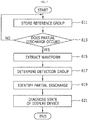
- FIG. 7 is a flowchart of a process of performing a self-diagnosis in relation to a partial discharge, the process performed by the display device 100, according to an embodiment of the present disclosure.
- the memory 240 of FIG. 2 may store a plurality of reference groups.
- the plurality of reference groups may represent waveforms of partial discharges which may occur in the converter 210 of FIG. 2 .
- each of the plurality of reference groups may be formed based on the genetic algorithm. That is, each of the plurality of reference groups may consist of bits determined to correspond to a predetermined number of parameters, e.g., N parameters, from one of the waveforms.
- the bits may be consecutively arranged in a predetermined order.
- Each of the parameters may correspond to one of the bits, expressed in the form of a binary number, i.e., 0 or 1.
- the memory 240 may store identification information to be mapped to each of the plurality of reference groups.
- the identification information may include at least one among a cause of a partial discharge, a location at which the partial discharge has occurred, and a degree of risk of the partial discharge.
- the degree of risk of the partial discharge may vary according to at least one of the cause of the partial discharge, the location at which the partial discharge has occurred, and a frequency of occurrence of the partial discharge.
- the memory 240 may store the plurality of reference groups as illustrated in FIG. 5 .
- the controller 230 of FIG. 2 may update the plurality of reference groups stored in the memory 240 on the basis of the genetic algorithm. To this end, the controller 230 may perform an operation on at least one of the plurality of reference groups. For example, the controller 230 may perform at least one among the selection operation 511, the crossover operation 513, the mutation operation 515, and the substitution operation 517 as illustrated in FIG. 6 .
- the detector 220 of FIG. 2 may detect the partial discharge.
- the detector 220 or 300 may detect the partial discharge in response to an input signal transmitted from the converter 210.
- the detector 220 or 300 may extract a waveform of the partial discharge.
- the detector 220 or 300 may extract the waveform of the partial discharge by removing a noise signal from the input signal.
- the detector 220 or 300 may determine a detection group from the waveform of the partial discharge.
- the detector 220 or 300 may measure a predetermined number of parameters, e.g., N parameters, from the waveform of the partial discharge.
- the parameters may include at least one among a phase of the partial discharge, a magnitude of the partial discharge, a frequency of occurrence of the partial discharge, a maximum magnitude of the partial discharge, an average discharge amount, a firing voltage, and an extinction voltage.
- the detector 220 or 300 may determine the detection group on the basis of the genetic algorithm. That is, the detector 220 or 300 may measure each of the parameters in the form of a binary number. Here, the detector 220 or 300 may measure each of the parameters in the form of a bit and express each of the parameters as 0 or 1. For example, the detector 220 or 300 may determine a bit corresponding to each of the parameters according to whether each of the parameters is greater than a predetermined threshold value. The detector 220 or 300 may determine the detection group by consecutively arranging the bits corresponding to the parameters in a predetermined order. For example, the detection group may be expressed as (0 0 1 0 1 1).
- the controller 230 may identify the partial discharge.
- the controller 230 may compare the detection group with the plurality of reference groups. That is, the controller 230 may determine whether the detection group is identical to one of the plurality of reference groups.
- the controller 230 may check identification information of the reference group identical to the detection group.
- the controller 230 may update the identification information of the reference group identical to the detection group. For example, when the detection group is identical to a reference group B, the controller 230 may increase a degree of risk of the reference group B.
- the controller 230 may diagnose a state of the display device 100 in response to the partial discharge.
- the controller 230 may diagnose the state of the display device 100 on the basis of the identification information of the reference group identical to the detection group.
- the controller 230 may predict a degree of deterioration of the converter 210 by analyzing the identification information of the reference group identical to the detection group. For example, the controller 230 predict the degree of deterioration of the converter 210 on the basis of at least one among the cause of the partial discharge, the location at which the partial discharge has occurred, and the degree of risk of the partial discharge.
- the controller 230 may diagnose the degree of deterioration of the converter 210 by comparing the degree of risk of the partial discharge with at least one predetermined threshold value. For example, when the degree of risk of the partial discharge is greater than or equal to the at least one predetermined threshold value, the controller 230 may output an alarm message to repair, inspect, or replace the converter 210.
- the controller 230 may power off the display device 100.
- the controller 230 may output the alarm message.
- the controller 230 may power off the display device 100.
- the controller 230 may output the alarm message and power off the display device 100.
- the display device 100 may identify the partial discharge by detecting a waveform of the partial discharge occurring in the converter 210. Thus, the display device 100 may perform a self-diagnosis in relation to the partial discharge.
- the display device 100 may output the alarm message to inform a user or a manager of the display device 100 that the converter 210 needs to be repaired, inspected, or replaced.
- the display device 100 may be powered off before it malfunctions.
- the display device 100 may be prevented from malfunctioning and thus can be used for a longer time period.
- a display device may identify a partial discharge by detecting a waveform of the partial discharge. That is, the display device may perform a self-diagnosis in relation to the partial discharge.
- the display device may output an alarm message to inform a user or a manger of the display device that the display device needs to be repaired, inspected, or replaced.
- the display device may be powered off before malfunctioning. Accordingly, the display device may be prevented from malfunctioning and thus the lifespan thereof may be improved.
Landscapes
- Engineering & Computer Science (AREA)
- Physics & Mathematics (AREA)
- General Physics & Mathematics (AREA)
- Theoretical Computer Science (AREA)
- General Engineering & Computer Science (AREA)
- Quality & Reliability (AREA)
- Optics & Photonics (AREA)
- Nonlinear Science (AREA)
- Computer Hardware Design (AREA)
- Chemical & Material Sciences (AREA)
- Crystallography & Structural Chemistry (AREA)
- Human Computer Interaction (AREA)
- Biomedical Technology (AREA)
- Health & Medical Sciences (AREA)
- Testing Relating To Insulation (AREA)
- Testing Electric Properties And Detecting Electric Faults (AREA)
Abstract
Description
- The present disclosure relates to a display device capable of performing a self-diagnosis in relation to a partial discharge.
- Generally, a partial discharge may occur in a display device. That is, when a high electric field is concentrated on a particular portion of the display device, the partial discharge may occur at the particular portion of the display device on which the high electric field is concentrated.
- For example, the partial discharge may include at least one among a corona discharge, a surface discharge, and a void discharge.
- The display device may be deteriorated due to the partial discharge. When the partial discharge repeatedly occurs, a dielectric breakdown may occur in the display device. The dielectric breakdown may be a cause of malfunction of display device.
- The present disclosure is directed to a display device capable of performing a self-diagnosis in relation to a partial discharge and preventing a malfunction thereof.
- Aspects of the present disclosure are not limited thereto, and additional aspects and advantages of the present disclosure which are not mentioned herein may be understood from the following description and will be apparent from embodiments of the present disclosure. Furthermore, it will be apparent that the aspects and advantages of the present disclosure can be implemented by means defined in the claims and a combination of the means.
- To address the above-described problems, according to an aspect of the present disclosure, a display device includes an image processor configured to process an image signal, and a display unit configured to display the processed image signal.
- The image processor may include a detector configured to determine a group of parameters by detecting a waveform of a detected partial discharge and measuring each of parameters of the waveform in the form of a binary number, and a controller configured to identify the detected partial discharge by comparing the determined group with previously stored groups.
- The controller may include an arithmetic unit configured to update the previously stored groups by performing an operation on at least one among the previously stored groups.
- The arithmetic unit may be further configured to perform at least one of a selection operation of selecting at least one first group from among the previously stored groups, a crossover operation of generating a second group by combining parameters of at least two groups among the previously stored groups, a mutation operation of generating a third group by changing at least one of parameters of the first or second group, and a substitution operation of replacing one of the previously stored groups with the first group, the second group, or the third group.
- The parameters may include at least one of a phase of the partial discharge, a magnitude of the partial discharge, a frequency of occurrence of the partial discharge, a maximum magnitude of the partial discharge, an average discharge amount, a firing voltage, and an extinction voltage.
- The image processor may further include a memory in which identification information of the partial discharge is mapped to each of the previously stored groups.
- The identification information may include at least one of a cause of the partial discharge, a location at which the partial discharge has occurred, and a degree of risk of the partial discharge.
- The controller may be further configured to diagnose a state of the display device on the basis of the identification information of the detected partial discharge.
- The controller may output an alarm message or power off the display device on the basis of the identification information of the detected partial discharge.
- The detector may include a first impedance element configured to decrease an output impedance when the partial discharge occurs, a first condenser in which a dielectric breakdown occurs when the output impedance of the first impedance element decreases, a second condenser of which an output voltage increases when the dielectric breakdown occurs in the first condenser, a second impedance element to which the increased output voltage of the second condenser is applied, and a sensing element configured to sense the occurring partial discharge on the basis of a voltage input from the second impedance element.
- The image processor may further include a converter configured to output the image signal in the form of digital data to the display unit.
- The detector may detect a partial discharge occurring in the converter.
- The above and other objects, features and advantages of the present disclosure will become more apparent to those of ordinary skill in the art by describing in detail exemplary embodiments thereof with reference to the accompanying drawings, in which:
-
FIG. 1 is a block diagram illustrating an internal structure of a display device according to an embodiment of the present disclosure; -
FIG. 2 is a block diagram illustrating an internal structure of an image processor according to an embodiment of the present disclosure; -
FIG. 3 is a block diagram of a detector ofFIG. 2 ; -
FIG. 4 is a circuit diagram of a sensor ofFIG. 3 ; -
FIGS. 5 and6 are diagrams illustrating examples of a memory and a controller ofFIG. 2 ; and -
FIG. 7 is a flowchart of a process of performing a self-diagnosis in relation to a partial discharge, the process being performed by a display device, according to an embodiment of the present disclosure. - Hereinafter, exemplary embodiments of the present disclosure will be described in detail below with reference to the accompanying drawings. However, the technology set forth herein should not be construed as being limited thereto and should be understood to cover various modifications, equivalents, and/or alternatives. In relation to describing drawings, like elements may be denoted by like reference numerals.
- As used herein, the terms such as "include", "may include", "comprise", and "may comprise" specify the presence of stated features, values, functions, and elements, e.g., components, but do not preclude the presence or addition of one or more other features, values, functions, and elements.
- The terms such as "first" or "second" may be used herein to describe various elements regardless of an order and/or importance, and these elements should not be limited by these terms. These terms are only used to distinguish one element from another element.
-
FIG. 1 is a block diagram illustrating an internal structure of adisplay device 100 according to an embodiment of the present disclosure. - Referring to
FIG. 1 , thedisplay device 100 according to an embodiment of the present disclosure may display an image signal received from an external device (not shown). To this end, thedisplay device 100 may be connected to the external device via wire or wirelessly. Thedisplay device 100 may interface with the external device and receive the image signal from the external device. For example, the external device may include a circuit breaker, and thedisplay device 100 may be a liquid crystal display (LCD) device. That is, thedisplay device 100 may include adisplay unit 120 and animage processor 110. - The
display unit 120 may display the image signal. For example, thedisplay unit 120 may include an LCD panel. - The
image processor 110 may control overall operations of thedisplay device 100. In this case, theimage processor 110 may control thedisplay unit 120. Furthermore, theimage processor 110 may output the image signal received from the external device to thedisplay unit 120. Here, theimage processor 110 may process the image signal according to features and a size of thedisplay unit 120. - In one embodiment of the present disclosure, the
image processor 110 may identify a partial discharge occurring therein and perform a self-diagnosis. In this case, theimage processor 110 may control thedisplay device 100 in response to the partial discharge. -
FIG. 2 is a block diagram illustrating an internal structure of theimage processor 110 according to an embodiment of the present disclosure.FIG. 3 is a block diagram of a detector ofFIG. 2 .FIG. 4 is a circuit diagram of a sensor ofFIG. 3. FIGS. 5 and6 are diagrams illustrating examples of a memory and a controller ofFIG. 2 . - Referring to
FIG. 2 , an image processor 200 (or theimage processor 110 ofFIG. 1 according to an embodiment of the present disclosure may include aconverter 210, adetector 220, acontroller 230, and amemory 240. - The
converter 210 may convert an image signal according to features and a size of thedisplay unit 120 ofFIG. 1 . Furthermore, theconverter 210 may output the image signal to thedisplay unit 120. In this case, theconverter 210 may output the image signal in the form of digital data. To this end, theconverter 210 may be formed by mounting a plurality of components on a substrate. - In one embodiment, the
converter 210 may include an image decoder, an analog-digital converter (ADC), a scaler, and a power supply. - The image decoder may decode the image signal.
- The ADC may receive a synchronization signal and an RGB signal corresponding to the image signal, and convert the RGB signal from an analog signal to digital data on the basis of the synchronization signal.
- The scaler may scale the image signal and the RGB signal and output the scaled image signal and RGB signal to the
display unit 120. - The power supply may supply power to the
display unit 120. - In one embodiment of the present disclosure, a partial discharge may occur in the
converter 210. That is, when a high electric field is concentrated at a particular portion of theconverter 210, the partial discharge may occur at the particular portion of theconverter 210 on which the high electric field is concentrated. In this case, the partial discharge may occur at various locations and due to various causes. - For example, the partial discharge may include at least one among a corona discharge, a surface discharge, and a void discharge. Thus, the particular portion of the
converter 210 at which the partial discharge occurs may deteriorate. As the partial discharge repeatedly occurs, a dielectric breakdown may occur in theconverter 210. The dielectric breakdown may be a cause of malfunction of thedisplay device 100. - The
detector 220 may detect the partial discharge occurring in theconverter 210 by detecting a waveform of the partial discharge. Here, thedetector 220 may measure the waveform of the partial discharge in the form of data consisting of a plurality of bits. - As illustrated in
FIG. 3 , a detector 300 (or thedetector 220 ofFIG. 2 ) may include asensor 310, anextractor 320, and ameasurer 330. - The
sensor 310 may sense a partial discharge occurring in theconverter 210. In this case, thesensor 310 may sense the partial discharge in response to an input signal from theconverter 210. For example, thesensor 310 may include a ceramic coupler. - As illustrated in
FIG. 4 , a sensor 400 (or thesensor 310 ofFIG. 3 ) may include afirst impedance element 410, afirst condenser 420, asecond condenser 430, asecond impedance element 440, and asensing element 450. - The
first impedance element 410 may respond to a partial discharge. That is, when a partial discharge occurs in theconverter 210, an output impedance of thefirst impedance element 410 may decrease. - The
first condenser 420 may be connected in series to thefirst impedance element 410. When the output impedance of thefirst impedance element 410 decreases, a dielectric breakdown may occur in thefirst condenser 420. - The
second condenser 430 may be connected in series to thefirst impedance element 410 and connected in parallel to thefirst condenser 420. When a dielectric breakdown occurs in thefirst condenser 420, an output voltage of thesecond condenser 430 may increase. - The
second impedance element 440 may be connected in series to thesecond condenser 430. That is, the output voltage of thesecond condenser 430 may be applied to thesecond impedance element 440. - The
sensing element 450 may be connected to thesecond impedance element 440. Thesensing element 450 may sense the partial discharge on the basis of a voltage input from thesecond impedance element 440. - The
extractor 320 may extract a waveform of the partial discharge. In this case, theextractor 320 may extract the waveform of the partial discharge by removing a noise signal from an input signal. For example, theextractor 320 may include a finite impulse response (FIR) filter. - The
measurer 330 may measure a predetermined number of parameters, e.g., N parameters, from the waveform of the partial discharge. For example, the parameters may include at least one among a phase of the partial discharge, a magnitude of the partial discharge, a frequency of occurrence of the partial discharge, a maximum intensity of the partial discharge, an average discharge amount, a firing voltage, and an extinction voltage. - The
measurer 330 may determine a group of parameters on the basis of a genetic algorithm. That is, themeasurer 330 may measure each of the parameters in the form of a binary number. Here, themeasurer 330 may measure each of the parameters in the form of a bit and express each of the parameters as 0 or 1. For example, themeasurer 330 may determine a bit corresponding to each of the parameters according to whether each of the parameters is greater than a predetermined threshold value. Furthermore, themeasurer 330 may determine the group of the parameters by consecutively arranging the bits corresponding to the parameters in a predetermined order. The term "detection group" to be described below may be understood as a group determined by themeasurer 330. For example, the detection group maybe expressed as (0 0 1 0 1 1). - The
memory 240 may store programs for operating thedisplay device 100. In this case, thememory 240 may store a program for detecting a partial discharge occurring in theconverter 210. - The
memory 240 may store data generated during execution of the programs. - Furthermore, the
memory 240 may store a plurality of groups each representing waveforms of partial discharges which may occur in theconverter 210. The term "reference group" to be described below may be understood as a group stored in thememory 240. - For example, as illustrated in
FIG. 5 , thememory 240 may store a plurality of reference groups A, B, C and D. Here, each of the reference groups A, B, C and D may be formed based on the genetic algorithm. That is, each of the reference groups A, B, C and D may consist of bits determined to correspond to a predetermined number of parameters, e.g., N parameters, from one of waveforms. Here, the bits may be consecutively arranged in the predetermined order. Each of the parameters may correspond to one of the bits expressed in the form of a binary number, i.e., 0 or 1. - Furthermore, the
memory 240 may store identification information identifying a partial discharge which may occur in theconverter 210 to be mapped to one of the reference groups. Here, the identification information may include at least one among a cause of the partial discharge, a location at which the partial discharge has occurred, and a degree of risk of the partial discharge. For example, the degree of risk of the partial discharge may vary according to at least one among the cause of the partial discharge, the location on theconverter 210 at which the partial discharge has occurred, and a frequency of occurrence of the partial discharge. - The
controller 230 may control overall operations of thedisplay device 100 ofFIG. 1 . Furthermore, thecontroller 230 may identify a partial discharge detected in theconverter 210. To this end, thecontroller 230 may compare a detection group with the reference groups. - That is, the
controller 230 may determine whether the detection group is identical to one of the reference groups. When the detection group is identical to one of the reference groups, thecontroller 230 may check identification information of the reference group identical to the detection group. Here, thecontroller 230 may update the identification information of the reference group identical to the detection group. For example, when the detection group is identical to the reference group B, thecontroller 230 may increase a degree of risk of the reference group B. - In addition, the
controller 230 may diagnose a state of thedisplay device 100 in response to the partial discharge. Here, thecontroller 230 may diagnose the state of thedisplay device 100 on the basis of the identification information of the reference group identical to the detection group. - To this end, the
controller 230 may predict a degree of deterioration of theconverter 210 by analyzing the identification information of the reference group identical to the detection group. For example, thecontroller 230 may predict the degree of deterioration of theconverter 210 on the basis of at least one among the cause of the partial discharge, the location at which the partial discharge has occurred, and the degree of risk of the partial discharge. - The
controller 230 may diagnose the degree of deterioration of theconverter 210 by comparing the degree of risk of the partial discharge with at least one predetermined threshold value. - For example, when the degree of risk of the partial discharge is greater than or equal to the at least one predetermined threshold value, the
controller 230 may output an alarm message to repair, inspect, or replace theconverter 210. Thecontroller 230 may transmit the alarm message to an external device or display the alarm message via thedisplay unit 120. - When the degree of risk of the partial discharge is greater than or equal to the at least one predetermined threshold value, the
controller 230 may power off thedisplay device 100. - The
controller 230 may output the alarm message when the degree of risk of the partial discharge is greater than or equal to a first threshold value and is less than a second threshold value which is greater than the first threshold value. - When the degree of risk of the partial discharge is greater than or equal to the second threshold value, the
controller 230 may power off thedisplay device 100. Alternatively, when the degree of risk of the partial discharge is greater than or equal to the second threshold value, thecontroller 230 may output the alarm message and power off thedisplay device 100. That is, thecontroller 230 may output the alarm message or power off thedisplay device 100 on the basis of the degree of risk of the partial discharge which is identification information of the partial discharge. - The
controller 230 may update the reference groups on the basis of the genetic algorithm. To this end, thecontroller 230 may include an arithmetic unit (not shown). The arithmetic unit may perform an operation on at least one of the reference groups. - In this case, the arithmetic unit may perform at least one among a
selection operation 511, acrossover operation 513, amutation operation 515, and asubstitution operation 517 as illustrated inFIG. 6 . The arithmetic unit may perform theselection operation 511 to select at least one of the reference groups, i.e., a first group. For example, the arithmetic unit may select the reference groups A and D. - The arithmetic unit may perform the
crossover operation 513 to generate a second group by combining at least two groups from among the reference groups. For example, the arithmetic unit may divide the bits of each of the reference group A and the reference group D into two regions by a predetermined line of intersection. Here, the bits of each of the reference group A and the reference group D may be divided into a first region at one side of the line of intersection and a second region at another side of the line of intersection. - Thereafter, the arithmetic unit may cross one of the regions of the reference group A, e.g., a first region, and one of the regions of the reference group D, e.g., a second region.
- The arithmetic unit may perform the
mutation operation 515 to generate a third group by changing at least one of the first group and the second group. For example, the arithmetic unit may change at least one bit corresponding to a predetermined location among the bits to a predetermined value, e.g., 0 or 1. - By changing the at least one bit, the arithmetic unit may add the first group, the second group, or the third group as a new reference group. For example, the arithmetic unit may add a reference group E. The arithmetic unit may perform the
substitution operation 517 to replace one of the reference groups with one of the first to third groups. For example, the arithmetic unit may change the reference group C. -
FIG. 7 is a flowchart of a process of performing a self-diagnosis in relation to a partial discharge, the process performed by thedisplay device 100, according to an embodiment of the present disclosure. - Referring to
FIG. 7 , in the process of performing a self-diagnosis in relation to a partial discharge, the process performed by thedisplay device 100 ofFIG. 1 , first, inoperation 611, thememory 240 ofFIG. 2 may store a plurality of reference groups. The plurality of reference groups may represent waveforms of partial discharges which may occur in theconverter 210 ofFIG. 2 . - In this case, each of the plurality of reference groups may be formed based on the genetic algorithm. That is, each of the plurality of reference groups may consist of bits determined to correspond to a predetermined number of parameters, e.g., N parameters, from one of the waveforms. Here, the bits may be consecutively arranged in a predetermined order. Each of the parameters may correspond to one of the bits, expressed in the form of a binary number, i.e., 0 or 1.
- The
memory 240 may store identification information to be mapped to each of the plurality of reference groups. Here, the identification information may include at least one among a cause of a partial discharge, a location at which the partial discharge has occurred, and a degree of risk of the partial discharge. For example, the degree of risk of the partial discharge may vary according to at least one of the cause of the partial discharge, the location at which the partial discharge has occurred, and a frequency of occurrence of the partial discharge. For example, thememory 240 may store the plurality of reference groups as illustrated inFIG. 5 . - The
controller 230 ofFIG. 2 may update the plurality of reference groups stored in thememory 240 on the basis of the genetic algorithm. To this end, thecontroller 230 may perform an operation on at least one of the plurality of reference groups. For example, thecontroller 230 may perform at least one among theselection operation 511, thecrossover operation 513, themutation operation 515, and thesubstitution operation 517 as illustrated inFIG. 6 . - Next, in
operation 613, when a partial discharge occurs in theconverter 210, thedetector 220 ofFIG. 2 (or thedetector 300 ofFIG. 3 ) may detect the partial discharge. In this case, thedetector converter 210. - Next, in
operation 615, thedetector detector - Next, in
operation 617, thedetector detector - The
detector detector detector detector detector - Next, in
operation 619, thecontroller 230 may identify the partial discharge. In this case, thecontroller 230 may compare the detection group with the plurality of reference groups. That is, thecontroller 230 may determine whether the detection group is identical to one of the plurality of reference groups. When the detection group is identical to one of the plurality of reference groups, thecontroller 230 may check identification information of the reference group identical to the detection group. Here, thecontroller 230 may update the identification information of the reference group identical to the detection group. For example, when the detection group is identical to a reference group B, thecontroller 230 may increase a degree of risk of the reference group B. - Lastly, in
operation 621, thecontroller 230 may diagnose a state of thedisplay device 100 in response to the partial discharge. In this case, thecontroller 230 may diagnose the state of thedisplay device 100 on the basis of the identification information of the reference group identical to the detection group. To this end, thecontroller 230 may predict a degree of deterioration of theconverter 210 by analyzing the identification information of the reference group identical to the detection group. For example, thecontroller 230 predict the degree of deterioration of theconverter 210 on the basis of at least one among the cause of the partial discharge, the location at which the partial discharge has occurred, and the degree of risk of the partial discharge. - The
controller 230 may diagnose the degree of deterioration of theconverter 210 by comparing the degree of risk of the partial discharge with at least one predetermined threshold value. For example, when the degree of risk of the partial discharge is greater than or equal to the at least one predetermined threshold value, thecontroller 230 may output an alarm message to repair, inspect, or replace theconverter 210. - When the degree of risk of the partial discharge is greater than or equal to the at least one predetermined threshold value, the
controller 230 may power off thedisplay device 100. - When the degree of risk of the partial discharge is greater than or equal to a first threshold value and is less than a second threshold value which is greater than the first threshold value, the
controller 230 may output the alarm message. - When the degree of risk of the partial discharge is greater than or equal to the second threshold value, the
controller 230 may power off thedisplay device 100. Alternatively, when the degree of risk of the partial discharge is greater than or equal to the second threshold value, thecontroller 230 may output the alarm message and power off thedisplay device 100. - The
display device 100 may identify the partial discharge by detecting a waveform of the partial discharge occurring in theconverter 210. Thus, thedisplay device 100 may perform a self-diagnosis in relation to the partial discharge. - In this case, the
display device 100 may output the alarm message to inform a user or a manager of thedisplay device 100 that theconverter 210 needs to be repaired, inspected, or replaced. - The
display device 100 may be powered off before it malfunctions. - Accordingly, the
display device 100 may be prevented from malfunctioning and thus can be used for a longer time period. - As described above, a display device may identify a partial discharge by detecting a waveform of the partial discharge. That is, the display device may perform a self-diagnosis in relation to the partial discharge.
- When the partial discharge is detected by performing the self-diagnosis, the display device may output an alarm message to inform a user or a manger of the display device that the display device needs to be repaired, inspected, or replaced.
- Alternatively, the display device may be powered off before malfunctioning. Accordingly, the display device may be prevented from malfunctioning and thus the lifespan thereof may be improved.
- The terminology used herein is for the purpose of describing particular embodiments only and is not intended to be limiting of the scopes of other embodiments. As used herein, the singular forms "a", "an" and "the" are intended to include the plural forms as well, unless the context clearly indicates otherwise. All terms (including technical and scientific terms) used herein have the same meaning as commonly understood by one of ordinary skill in the art set forth herein. It will be further understood that terms, such as those defined in commonly used dictionaries, should be interpreted as having a meaning that is consistent with their meaning in the context of the relevant art and will not be interpreted in an idealized or overly formal sense unless expressly so defined herein. In some cases, even terms defined herein should not be understood to exclude the embodiments set forth herein.
Claims (10)
- A display device (100) capable of performing a self-diagnosis in relation to a partial discharge, the display device comprising:an image processor (110) configured to process an image signal; anda display unit (120) configured to display the processed image signal,wherein the image processor (110)(200) comprises:a detector (220) configured to determine a group of parameters by detecting a waveform of a detected partial discharge and measuring each of parameters of the waveform in the form of a binary number; anda controller (230) configured to identify the detected partial discharge by comparing the determined group with previously stored groups.
- The display device of claim 1, wherein the controller (230) comprises an arithmetic unit configured to update the previously stored groups by performing an operation on at least one among the previously stored groups.
- The display device of claim 2, wherein the arithmetic unit is further configured to perform at least one of:a selection operation of selecting at least one first group from among the previously stored groups;a crossover operation of generating a second group by combining parameters of at least two groups among the previously stored groups;a mutation operation of generating a third group by changing at least one of parameters of the first or second group; anda substitution operation of replacing one of the previously stored groups with the first group, the second group, or the third group.
- The display device of any one of claims 1 to 3, wherein the parameters comprise at least one of:a phase of the partial discharge;a magnitude of the partial discharge;a frequency of occurrence of the partial discharge;a maximum magnitude of the partial discharge;an average discharge amount;a firing voltage; andan extinction voltage.
- The display device of any one of claims 1 to 4, wherein the image processor (200) further comprises a memory (240) in which identification information of the partial discharge is mapped to each of the previously stored groups.
- The display device of claim 5, wherein the identification information comprises at least one of:a cause of the partial discharge;a location at which the partial discharge occurs; anda degree of risk of the partial discharge.
- The display device of claim 5, wherein the controller (230) is further configured to diagnose a state of the display device on the basis of the identification information of the detected partial discharge.
- The display device of claim 7, wherein the controller (230) outputs an alarm message or powers off the display device on the basis of the identification information of the detected partial discharge.
- The display device of claim 1, wherein the detector (220) comprises:a first impedance element (410) configured to decrease an output impedance when the partial discharge occurs;a first condenser (420) in which a dielectric breakdown occurs when the output impedance of the first impedance element decreases;a second condenser (430) of which an output voltage increases when the dielectric breakdown occurs in the first condenser;a second impedance element (440) to which the increased output voltage of the second condenser is applied; anda sensing element (450) configured to sense the occurring partial discharge on the basis of a voltage input from the second impedance element.
- The display device of any one of claims 1 to 9, wherein the image processor (200) further comprises a converter (210) configured to output the image signal in the form of digital data to the display unit, and
the detector (220) detects a partial discharge occurring in the converter.
Applications Claiming Priority (1)
| Application Number | Priority Date | Filing Date | Title |
|---|---|---|---|
| KR1020170164260A KR102011459B1 (en) | 2017-12-01 | 2017-12-01 | Display device capable of self diagnosis for partial discharge |
Publications (2)
| Publication Number | Publication Date |
|---|---|
| EP3492940A1 true EP3492940A1 (en) | 2019-06-05 |
| EP3492940B1 EP3492940B1 (en) | 2022-03-02 |
Family
ID=63579116
Family Applications (1)
| Application Number | Title | Priority Date | Filing Date |
|---|---|---|---|
| EP18194136.0A Active EP3492940B1 (en) | 2017-12-01 | 2018-09-12 | Display device capable of performing self-diagnosis in relation to partial discharge |
Country Status (5)
| Country | Link |
|---|---|
| US (1) | US10853156B2 (en) |
| EP (1) | EP3492940B1 (en) |
| KR (1) | KR102011459B1 (en) |
| CN (1) | CN109872703B (en) |
| ES (1) | ES2913265T3 (en) |
Cited By (1)
| Publication number | Priority date | Publication date | Assignee | Title |
|---|---|---|---|---|
| CN118425709A (en) * | 2024-07-04 | 2024-08-02 | 中国南方电网有限责任公司超高压输电公司电力科研院 | Partial discharge detection method and device |
Citations (4)
| Publication number | Priority date | Publication date | Assignee | Title |
|---|---|---|---|---|
| US20030122749A1 (en) * | 2001-12-31 | 2003-07-03 | Booth Lawrence A. | Energy sensing light emitting diode display |
| EP1335430A1 (en) * | 2002-02-12 | 2003-08-13 | Eastman Kodak Company | A flat-panel light emitting pixel with luminance feedback |
| JP2008216334A (en) * | 2007-02-28 | 2008-09-18 | Nippon Signal Co Ltd:The | Detecting method and detecting device for screen display fault |
| US20160055778A1 (en) * | 2014-08-22 | 2016-02-25 | Lg Electronics Inc. | Self-diagnosing system and method of self-diagnosing of a display device |
Family Cites Families (19)
| Publication number | Priority date | Publication date | Assignee | Title |
|---|---|---|---|---|
| JP3092335B2 (en) * | 1992-06-26 | 2000-09-25 | 日立電線株式会社 | Identification method of partial discharge pulse |
| DE10316901A1 (en) * | 2003-04-12 | 2004-10-28 | Roche Diagnostics Gmbh | Control system and control method for checking the function of LCD displays |
| TW594655B (en) * | 2003-07-11 | 2004-06-21 | Toppoly Optoelectronics Corp | Testing circuit and method thereof for a flat panel display |
| GB0517994D0 (en) * | 2005-09-05 | 2005-10-12 | Univ Glasgow | High voltage insulation monitoring sensor |
| TWI308640B (en) * | 2006-12-27 | 2009-04-11 | Ind Tech Res Inst | Portable partial discharge detection device and method thereof |
| IT1394479B1 (en) * | 2009-05-29 | 2012-07-05 | Techimp Technologies S A Ora Techimp Technologies S R L | INSTRUMENT AND PROCEDURE FOR DETECTION OF PARTIAL ELECTRIC DISCHARGES IN AN ELECTRIC EQUIPMENT. |
| IT1396358B1 (en) * | 2009-10-30 | 2012-11-19 | Techimp Technologies S A Ora Techimp Technologies S R L | DEVICE AND PROCEDURE TO DETECT AND PROCESS SIGNALS RELATED TO PARTIAL ELECTRICAL DISCHARGE. |
| KR20110083823A (en) * | 2010-01-15 | 2011-07-21 | 삼성전자주식회사 | Arc noise detection circuit, light source driving apparatus including same and light source driving method using same |
| CN101907665A (en) * | 2010-07-16 | 2010-12-08 | 西安交通大学 | Fault Diagnosis Method of Oil-immersed Power Equipment Combined with Fuzzy Theory and Improved Genetic Algorithm |
| CN102163186B (en) * | 2011-04-18 | 2013-04-17 | 广东电网公司电力科学研究院 | Method and device for detecting generated file of local discharging signal of high-voltage power equipment |
| CN102353877B (en) * | 2011-06-10 | 2013-12-18 | 河南电力试验研究院 | Partial discharge detection method for realizing phase resolved partial discharge (PRPD) pattern and time resolved partial discharge (TRPD) pattern |
| JP2015040763A (en) * | 2013-08-22 | 2015-03-02 | 株式会社日立製作所 | Partial discharge measuring apparatus and method |
| KR101635861B1 (en) | 2014-10-07 | 2016-07-05 | 주식회사 코리아나화장품 | Oral composition containing fermentative extract of galla rhoids as active ingredient |
| KR102244716B1 (en) * | 2014-10-17 | 2021-04-28 | 한국전력공사 | Apparatus for analyzing pattern of partial discharge and detecting location of partial discharge |
| CN107110909B (en) | 2014-12-01 | 2019-11-15 | 住友电气工业株式会社 | Partial discharge determination device and partial discharge determination method |
| CN104965158B (en) * | 2015-05-21 | 2018-02-09 | 武汉大学 | A kind of improved high-frequency local discharging electric power detection harvester and method |
| CN104865511A (en) * | 2015-06-23 | 2015-08-26 | 国家电网公司 | Partial discharge detection device |
| KR102472783B1 (en) * | 2016-02-29 | 2022-12-02 | 삼성디스플레이 주식회사 | Display device and method of compensating degradation |
| US10460638B2 (en) * | 2017-04-26 | 2019-10-29 | Honeywell International Inc. | Intermittent display issue monitoring system |
-
2017
- 2017-12-01 KR KR1020170164260A patent/KR102011459B1/en active Active
-
2018
- 2018-09-11 CN CN201811055615.9A patent/CN109872703B/en active Active
- 2018-09-12 ES ES18194136T patent/ES2913265T3/en active Active
- 2018-09-12 EP EP18194136.0A patent/EP3492940B1/en active Active
- 2018-09-13 US US16/130,318 patent/US10853156B2/en active Active
Patent Citations (4)
| Publication number | Priority date | Publication date | Assignee | Title |
|---|---|---|---|---|
| US20030122749A1 (en) * | 2001-12-31 | 2003-07-03 | Booth Lawrence A. | Energy sensing light emitting diode display |
| EP1335430A1 (en) * | 2002-02-12 | 2003-08-13 | Eastman Kodak Company | A flat-panel light emitting pixel with luminance feedback |
| JP2008216334A (en) * | 2007-02-28 | 2008-09-18 | Nippon Signal Co Ltd:The | Detecting method and detecting device for screen display fault |
| US20160055778A1 (en) * | 2014-08-22 | 2016-02-25 | Lg Electronics Inc. | Self-diagnosing system and method of self-diagnosing of a display device |
Cited By (1)
| Publication number | Priority date | Publication date | Assignee | Title |
|---|---|---|---|---|
| CN118425709A (en) * | 2024-07-04 | 2024-08-02 | 中国南方电网有限责任公司超高压输电公司电力科研院 | Partial discharge detection method and device |
Also Published As
| Publication number | Publication date |
|---|---|
| CN109872703A (en) | 2019-06-11 |
| US10853156B2 (en) | 2020-12-01 |
| KR20190064924A (en) | 2019-06-11 |
| EP3492940B1 (en) | 2022-03-02 |
| KR102011459B1 (en) | 2019-08-19 |
| CN109872703B (en) | 2022-04-15 |
| ES2913265T3 (en) | 2022-06-01 |
| US20190170806A1 (en) | 2019-06-06 |
Similar Documents
| Publication | Publication Date | Title |
|---|---|---|
| US10571504B2 (en) | Diagnostic system for electric power equipment | |
| JP7370693B2 (en) | Partial discharge detection system, learning system, partial discharge detection method, computer program and electrical equipment | |
| US20120075755A1 (en) | Electric device, electric device system, method to detect arc fault in the same | |
| KR101930593B1 (en) | Display apparatus with testing functions and driving circuit and driving method thereof | |
| CN103048613A (en) | Systems and methods for monitoring electrical contacts | |
| KR102368180B1 (en) | Arc detection method and apparatus using variation of magnitude by frequency | |
| CN104348253A (en) | Methods and systems for monitoring devices in a power distribution system | |
| US20170032654A1 (en) | Power failure monitoring device of digital protection relay | |
| JP2010281673A (en) | Partial discharge voltage measurement system and partial discharge voltage measurement method | |
| JP5511639B2 (en) | Partial discharge analyzer | |
| US10853156B2 (en) | Display device capable of performing self diagnosis in relation to partial discharge | |
| CN101614758B (en) | Electronic type indicator | |
| JP6878057B2 (en) | Insulation diagnostic equipment and insulation diagnostic method | |
| JP4817819B2 (en) | Waveform display device | |
| JP7398634B2 (en) | Deterioration detection method, program and deterioration detection system | |
| JP2012150110A (en) | Method and system including monitor operation of circuit connectivity | |
| TWI664822B (en) | Signal processing apparatus and testing method | |
| KR101474848B1 (en) | Lifetime estimating and management device of surge protector | |
| KR101715778B1 (en) | Method for measuring power dissitation in electric power grid | |
| WO2020059384A1 (en) | Seismic sensor and sensor control method | |
| JP2010044013A (en) | Method of testing semiconductor device | |
| US20220230530A1 (en) | Fire alarm system | |
| JP7189853B2 (en) | vehicle control system | |
| JP2014016171A (en) | Inspection system and signal generation device | |
| JP6608801B2 (en) | High voltage power supply device and notification method |
Legal Events
| Date | Code | Title | Description |
|---|---|---|---|
| PUAI | Public reference made under article 153(3) epc to a published international application that has entered the european phase |
Free format text: ORIGINAL CODE: 0009012 |
|
| STAA | Information on the status of an ep patent application or granted ep patent |
Free format text: STATUS: THE APPLICATION HAS BEEN PUBLISHED |
|
| AK | Designated contracting states |
Kind code of ref document: A1 Designated state(s): AL AT BE BG CH CY CZ DE DK EE ES FI FR GB GR HR HU IE IS IT LI LT LU LV MC MK MT NL NO PL PT RO RS SE SI SK SM TR |
|
| AX | Request for extension of the european patent |
Extension state: BA ME |
|
| STAA | Information on the status of an ep patent application or granted ep patent |
Free format text: STATUS: REQUEST FOR EXAMINATION WAS MADE |
|
| 17P | Request for examination filed |
Effective date: 20191205 |
|
| RBV | Designated contracting states (corrected) |
Designated state(s): AL AT BE BG CH CY CZ DE DK EE ES FI FR GB GR HR HU IE IS IT LI LT LU LV MC MK MT NL NO PL PT RO RS SE SI SK SM TR |
|
| STAA | Information on the status of an ep patent application or granted ep patent |
Free format text: STATUS: EXAMINATION IS IN PROGRESS |
|
| 17Q | First examination report despatched |
Effective date: 20210326 |
|
| GRAP | Despatch of communication of intention to grant a patent |
Free format text: ORIGINAL CODE: EPIDOSNIGR1 |
|
| STAA | Information on the status of an ep patent application or granted ep patent |
Free format text: STATUS: GRANT OF PATENT IS INTENDED |
|
| INTG | Intention to grant announced |
Effective date: 20211019 |
|
| GRAS | Grant fee paid |
Free format text: ORIGINAL CODE: EPIDOSNIGR3 |
|
| GRAA | (expected) grant |
Free format text: ORIGINAL CODE: 0009210 |
|
| STAA | Information on the status of an ep patent application or granted ep patent |
Free format text: STATUS: THE PATENT HAS BEEN GRANTED |
|
| AK | Designated contracting states |
Kind code of ref document: B1 Designated state(s): AL AT BE BG CH CY CZ DE DK EE ES FI FR GB GR HR HU IE IS IT LI LT LU LV MC MK MT NL NO PL PT RO RS SE SI SK SM TR |
|
| REG | Reference to a national code |
Ref country code: GB Ref legal event code: FG4D |
|
| REG | Reference to a national code |
Ref country code: CH Ref legal event code: EP Ref country code: AT Ref legal event code: REF Ref document number: 1472693 Country of ref document: AT Kind code of ref document: T Effective date: 20220315 |
|
| REG | Reference to a national code |
Ref country code: DE Ref legal event code: R096 Ref document number: 602018031501 Country of ref document: DE |
|
| REG | Reference to a national code |
Ref country code: IE Ref legal event code: FG4D |
|
| REG | Reference to a national code |
Ref country code: ES Ref legal event code: FG2A Ref document number: 2913265 Country of ref document: ES Kind code of ref document: T3 Effective date: 20220601 |
|
| REG | Reference to a national code |
Ref country code: LT Ref legal event code: MG9D |
|
| REG | Reference to a national code |
Ref country code: NL Ref legal event code: MP Effective date: 20220302 |
|
| PG25 | Lapsed in a contracting state [announced via postgrant information from national office to epo] |
Ref country code: SE Free format text: LAPSE BECAUSE OF FAILURE TO SUBMIT A TRANSLATION OF THE DESCRIPTION OR TO PAY THE FEE WITHIN THE PRESCRIBED TIME-LIMIT Effective date: 20220302 Ref country code: RS Free format text: LAPSE BECAUSE OF FAILURE TO SUBMIT A TRANSLATION OF THE DESCRIPTION OR TO PAY THE FEE WITHIN THE PRESCRIBED TIME-LIMIT Effective date: 20220302 Ref country code: NO Free format text: LAPSE BECAUSE OF FAILURE TO SUBMIT A TRANSLATION OF THE DESCRIPTION OR TO PAY THE FEE WITHIN THE PRESCRIBED TIME-LIMIT Effective date: 20220602 Ref country code: LT Free format text: LAPSE BECAUSE OF FAILURE TO SUBMIT A TRANSLATION OF THE DESCRIPTION OR TO PAY THE FEE WITHIN THE PRESCRIBED TIME-LIMIT Effective date: 20220302 Ref country code: HR Free format text: LAPSE BECAUSE OF FAILURE TO SUBMIT A TRANSLATION OF THE DESCRIPTION OR TO PAY THE FEE WITHIN THE PRESCRIBED TIME-LIMIT Effective date: 20220302 Ref country code: BG Free format text: LAPSE BECAUSE OF FAILURE TO SUBMIT A TRANSLATION OF THE DESCRIPTION OR TO PAY THE FEE WITHIN THE PRESCRIBED TIME-LIMIT Effective date: 20220602 |
|
| REG | Reference to a national code |
Ref country code: AT Ref legal event code: MK05 Ref document number: 1472693 Country of ref document: AT Kind code of ref document: T Effective date: 20220302 |
|
| PG25 | Lapsed in a contracting state [announced via postgrant information from national office to epo] |
Ref country code: PL Free format text: LAPSE BECAUSE OF FAILURE TO SUBMIT A TRANSLATION OF THE DESCRIPTION OR TO PAY THE FEE WITHIN THE PRESCRIBED TIME-LIMIT Effective date: 20220302 Ref country code: LV Free format text: LAPSE BECAUSE OF FAILURE TO SUBMIT A TRANSLATION OF THE DESCRIPTION OR TO PAY THE FEE WITHIN THE PRESCRIBED TIME-LIMIT Effective date: 20220302 Ref country code: GR Free format text: LAPSE BECAUSE OF FAILURE TO SUBMIT A TRANSLATION OF THE DESCRIPTION OR TO PAY THE FEE WITHIN THE PRESCRIBED TIME-LIMIT Effective date: 20220603 Ref country code: FI Free format text: LAPSE BECAUSE OF FAILURE TO SUBMIT A TRANSLATION OF THE DESCRIPTION OR TO PAY THE FEE WITHIN THE PRESCRIBED TIME-LIMIT Effective date: 20220302 |
|
| PG25 | Lapsed in a contracting state [announced via postgrant information from national office to epo] |
Ref country code: NL Free format text: LAPSE BECAUSE OF FAILURE TO SUBMIT A TRANSLATION OF THE DESCRIPTION OR TO PAY THE FEE WITHIN THE PRESCRIBED TIME-LIMIT Effective date: 20220302 |
|
| PG25 | Lapsed in a contracting state [announced via postgrant information from national office to epo] |
Ref country code: SM Free format text: LAPSE BECAUSE OF FAILURE TO SUBMIT A TRANSLATION OF THE DESCRIPTION OR TO PAY THE FEE WITHIN THE PRESCRIBED TIME-LIMIT Effective date: 20220302 Ref country code: SK Free format text: LAPSE BECAUSE OF FAILURE TO SUBMIT A TRANSLATION OF THE DESCRIPTION OR TO PAY THE FEE WITHIN THE PRESCRIBED TIME-LIMIT Effective date: 20220302 Ref country code: RO Free format text: LAPSE BECAUSE OF FAILURE TO SUBMIT A TRANSLATION OF THE DESCRIPTION OR TO PAY THE FEE WITHIN THE PRESCRIBED TIME-LIMIT Effective date: 20220302 Ref country code: PT Free format text: LAPSE BECAUSE OF FAILURE TO SUBMIT A TRANSLATION OF THE DESCRIPTION OR TO PAY THE FEE WITHIN THE PRESCRIBED TIME-LIMIT Effective date: 20220704 Ref country code: EE Free format text: LAPSE BECAUSE OF FAILURE TO SUBMIT A TRANSLATION OF THE DESCRIPTION OR TO PAY THE FEE WITHIN THE PRESCRIBED TIME-LIMIT Effective date: 20220302 Ref country code: CZ Free format text: LAPSE BECAUSE OF FAILURE TO SUBMIT A TRANSLATION OF THE DESCRIPTION OR TO PAY THE FEE WITHIN THE PRESCRIBED TIME-LIMIT Effective date: 20220302 Ref country code: AT Free format text: LAPSE BECAUSE OF FAILURE TO SUBMIT A TRANSLATION OF THE DESCRIPTION OR TO PAY THE FEE WITHIN THE PRESCRIBED TIME-LIMIT Effective date: 20220302 |
|
| PG25 | Lapsed in a contracting state [announced via postgrant information from national office to epo] |
Ref country code: IS Free format text: LAPSE BECAUSE OF FAILURE TO SUBMIT A TRANSLATION OF THE DESCRIPTION OR TO PAY THE FEE WITHIN THE PRESCRIBED TIME-LIMIT Effective date: 20220702 Ref country code: AL Free format text: LAPSE BECAUSE OF FAILURE TO SUBMIT A TRANSLATION OF THE DESCRIPTION OR TO PAY THE FEE WITHIN THE PRESCRIBED TIME-LIMIT Effective date: 20220302 |
|
| REG | Reference to a national code |
Ref country code: DE Ref legal event code: R097 Ref document number: 602018031501 Country of ref document: DE |
|
| PLBE | No opposition filed within time limit |
Free format text: ORIGINAL CODE: 0009261 |
|
| STAA | Information on the status of an ep patent application or granted ep patent |
Free format text: STATUS: NO OPPOSITION FILED WITHIN TIME LIMIT |
|
| PG25 | Lapsed in a contracting state [announced via postgrant information from national office to epo] |
Ref country code: DK Free format text: LAPSE BECAUSE OF FAILURE TO SUBMIT A TRANSLATION OF THE DESCRIPTION OR TO PAY THE FEE WITHIN THE PRESCRIBED TIME-LIMIT Effective date: 20220302 |
|
| 26N | No opposition filed |
Effective date: 20221205 |
|
| PG25 | Lapsed in a contracting state [announced via postgrant information from national office to epo] |
Ref country code: SI Free format text: LAPSE BECAUSE OF FAILURE TO SUBMIT A TRANSLATION OF THE DESCRIPTION OR TO PAY THE FEE WITHIN THE PRESCRIBED TIME-LIMIT Effective date: 20220302 |
|
| PG25 | Lapsed in a contracting state [announced via postgrant information from national office to epo] |
Ref country code: MC Free format text: LAPSE BECAUSE OF FAILURE TO SUBMIT A TRANSLATION OF THE DESCRIPTION OR TO PAY THE FEE WITHIN THE PRESCRIBED TIME-LIMIT Effective date: 20220302 |
|
| REG | Reference to a national code |
Ref country code: CH Ref legal event code: PL |
|
| GBPC | Gb: european patent ceased through non-payment of renewal fee |
Effective date: 20220912 |
|
| REG | Reference to a national code |
Ref country code: BE Ref legal event code: MM Effective date: 20220930 |
|
| PG25 | Lapsed in a contracting state [announced via postgrant information from national office to epo] |
Ref country code: LU Free format text: LAPSE BECAUSE OF NON-PAYMENT OF DUE FEES Effective date: 20220912 |
|
| PG25 | Lapsed in a contracting state [announced via postgrant information from national office to epo] |
Ref country code: LI Free format text: LAPSE BECAUSE OF NON-PAYMENT OF DUE FEES Effective date: 20220930 Ref country code: IE Free format text: LAPSE BECAUSE OF NON-PAYMENT OF DUE FEES Effective date: 20220912 Ref country code: CH Free format text: LAPSE BECAUSE OF NON-PAYMENT OF DUE FEES Effective date: 20220930 |
|
| P01 | Opt-out of the competence of the unified patent court (upc) registered |
Effective date: 20230625 |
|
| PG25 | Lapsed in a contracting state [announced via postgrant information from national office to epo] |
Ref country code: BE Free format text: LAPSE BECAUSE OF NON-PAYMENT OF DUE FEES Effective date: 20220930 |
|
| PG25 | Lapsed in a contracting state [announced via postgrant information from national office to epo] |
Ref country code: GB Free format text: LAPSE BECAUSE OF NON-PAYMENT OF DUE FEES Effective date: 20220912 |
|
| PG25 | Lapsed in a contracting state [announced via postgrant information from national office to epo] |
Ref country code: HU Free format text: LAPSE BECAUSE OF FAILURE TO SUBMIT A TRANSLATION OF THE DESCRIPTION OR TO PAY THE FEE WITHIN THE PRESCRIBED TIME-LIMIT; INVALID AB INITIO Effective date: 20180912 |
|
| PG25 | Lapsed in a contracting state [announced via postgrant information from national office to epo] |
Ref country code: CY Free format text: LAPSE BECAUSE OF FAILURE TO SUBMIT A TRANSLATION OF THE DESCRIPTION OR TO PAY THE FEE WITHIN THE PRESCRIBED TIME-LIMIT Effective date: 20220302 |
|
| PG25 | Lapsed in a contracting state [announced via postgrant information from national office to epo] |
Ref country code: MK Free format text: LAPSE BECAUSE OF FAILURE TO SUBMIT A TRANSLATION OF THE DESCRIPTION OR TO PAY THE FEE WITHIN THE PRESCRIBED TIME-LIMIT Effective date: 20220302 |
|
| PG25 | Lapsed in a contracting state [announced via postgrant information from national office to epo] |
Ref country code: MT Free format text: LAPSE BECAUSE OF FAILURE TO SUBMIT A TRANSLATION OF THE DESCRIPTION OR TO PAY THE FEE WITHIN THE PRESCRIBED TIME-LIMIT Effective date: 20220302 |
|
| PGFP | Annual fee paid to national office [announced via postgrant information from national office to epo] |
Ref country code: FR Payment date: 20250611 Year of fee payment: 8 |
|
| PGFP | Annual fee paid to national office [announced via postgrant information from national office to epo] |
Ref country code: DE Payment date: 20250609 Year of fee payment: 8 |
|
| PGFP | Annual fee paid to national office [announced via postgrant information from national office to epo] |
Ref country code: IT Payment date: 20250610 Year of fee payment: 8 |
|
| PG25 | Lapsed in a contracting state [announced via postgrant information from national office to epo] |
Ref country code: TR Free format text: LAPSE BECAUSE OF FAILURE TO SUBMIT A TRANSLATION OF THE DESCRIPTION OR TO PAY THE FEE WITHIN THE PRESCRIBED TIME-LIMIT Effective date: 20220302 |
|
| PGFP | Annual fee paid to national office [announced via postgrant information from national office to epo] |
Ref country code: ES Payment date: 20251008 Year of fee payment: 8 |