EP3492423A1 - Method for forming hermetic seals in mems devices - Google Patents
Method for forming hermetic seals in mems devices Download PDFInfo
- Publication number
- EP3492423A1 EP3492423A1 EP18207750.3A EP18207750A EP3492423A1 EP 3492423 A1 EP3492423 A1 EP 3492423A1 EP 18207750 A EP18207750 A EP 18207750A EP 3492423 A1 EP3492423 A1 EP 3492423A1
- Authority
- EP
- European Patent Office
- Prior art keywords
- wafer
- depressions
- indium
- resist
- adhesion
- Prior art date
- Legal status (The legal status is an assumption and is not a legal conclusion. Google has not performed a legal analysis and makes no representation as to the accuracy of the status listed.)
- Granted
Links
Images



Classifications
-
- B—PERFORMING OPERATIONS; TRANSPORTING
- B81—MICROSTRUCTURAL TECHNOLOGY
- B81C—PROCESSES OR APPARATUS SPECIALLY ADAPTED FOR THE MANUFACTURE OR TREATMENT OF MICROSTRUCTURAL DEVICES OR SYSTEMS
- B81C1/00—Manufacture or treatment of devices or systems in or on a substrate
- B81C1/00015—Manufacture or treatment of devices or systems in or on a substrate for manufacturing microsystems
- B81C1/00261—Processes for packaging MEMS devices
- B81C1/00269—Bonding of solid lids or wafers to the substrate
-
- B—PERFORMING OPERATIONS; TRANSPORTING
- B32—LAYERED PRODUCTS
- B32B—LAYERED PRODUCTS, i.e. PRODUCTS BUILT-UP OF STRATA OF FLAT OR NON-FLAT, e.g. CELLULAR OR HONEYCOMB, FORM
- B32B17/00—Layered products essentially comprising sheet glass, or glass, slag, or like fibres
- B32B17/06—Layered products essentially comprising sheet glass, or glass, slag, or like fibres comprising glass as the main or only constituent of a layer, next to another layer of a specific material
-
- B—PERFORMING OPERATIONS; TRANSPORTING
- B32—LAYERED PRODUCTS
- B32B—LAYERED PRODUCTS, i.e. PRODUCTS BUILT-UP OF STRATA OF FLAT OR NON-FLAT, e.g. CELLULAR OR HONEYCOMB, FORM
- B32B3/00—Layered products comprising a layer with external or internal discontinuities or unevennesses, or a layer of non-planar shape; Layered products comprising a layer having particular features of form
- B32B3/26—Layered products comprising a layer with external or internal discontinuities or unevennesses, or a layer of non-planar shape; Layered products comprising a layer having particular features of form characterised by a particular shape of the outline of the cross-section of a continuous layer; characterised by a layer with cavities or internal voids ; characterised by an apertured layer
- B32B3/30—Layered products comprising a layer with external or internal discontinuities or unevennesses, or a layer of non-planar shape; Layered products comprising a layer having particular features of form characterised by a particular shape of the outline of the cross-section of a continuous layer; characterised by a layer with cavities or internal voids ; characterised by an apertured layer characterised by a layer formed with recesses or projections, e.g. hollows, grooves, protuberances, ribs
-
- B—PERFORMING OPERATIONS; TRANSPORTING
- B32—LAYERED PRODUCTS
- B32B—LAYERED PRODUCTS, i.e. PRODUCTS BUILT-UP OF STRATA OF FLAT OR NON-FLAT, e.g. CELLULAR OR HONEYCOMB, FORM
- B32B37/00—Methods or apparatus for laminating, e.g. by curing or by ultrasonic bonding
- B32B37/12—Methods or apparatus for laminating, e.g. by curing or by ultrasonic bonding characterised by using adhesives
-
- B—PERFORMING OPERATIONS; TRANSPORTING
- B32—LAYERED PRODUCTS
- B32B—LAYERED PRODUCTS, i.e. PRODUCTS BUILT-UP OF STRATA OF FLAT OR NON-FLAT, e.g. CELLULAR OR HONEYCOMB, FORM
- B32B37/00—Methods or apparatus for laminating, e.g. by curing or by ultrasonic bonding
- B32B37/14—Methods or apparatus for laminating, e.g. by curing or by ultrasonic bonding characterised by the properties of the layers
- B32B37/16—Methods or apparatus for laminating, e.g. by curing or by ultrasonic bonding characterised by the properties of the layers with all layers existing as coherent layers before laminating
- B32B37/18—Methods or apparatus for laminating, e.g. by curing or by ultrasonic bonding characterised by the properties of the layers with all layers existing as coherent layers before laminating involving the assembly of discrete sheets or panels only
-
- B—PERFORMING OPERATIONS; TRANSPORTING
- B32—LAYERED PRODUCTS
- B32B—LAYERED PRODUCTS, i.e. PRODUCTS BUILT-UP OF STRATA OF FLAT OR NON-FLAT, e.g. CELLULAR OR HONEYCOMB, FORM
- B32B7/00—Layered products characterised by the relation between layers; Layered products characterised by the relative orientation of features between layers, or by the relative values of a measurable parameter between layers, i.e. products comprising layers having different physical, chemical or physicochemical properties; Layered products characterised by the interconnection of layers
- B32B7/04—Interconnection of layers
- B32B7/12—Interconnection of layers using interposed adhesives or interposed materials with bonding properties
-
- B—PERFORMING OPERATIONS; TRANSPORTING
- B32—LAYERED PRODUCTS
- B32B—LAYERED PRODUCTS, i.e. PRODUCTS BUILT-UP OF STRATA OF FLAT OR NON-FLAT, e.g. CELLULAR OR HONEYCOMB, FORM
- B32B9/00—Layered products comprising a layer of a particular substance not covered by groups B32B11/00 - B32B29/00
- B32B9/04—Layered products comprising a layer of a particular substance not covered by groups B32B11/00 - B32B29/00 comprising such particular substance as the main or only constituent of a layer, which is next to another layer of the same or of a different material
-
- B—PERFORMING OPERATIONS; TRANSPORTING
- B81—MICROSTRUCTURAL TECHNOLOGY
- B81B—MICROSTRUCTURAL DEVICES OR SYSTEMS, e.g. MICROMECHANICAL DEVICES
- B81B7/00—Microstructural systems ; Auxiliary parts of microstructural devices or systems
- B81B7/0032—Packages or encapsulation
- B81B7/0035—Packages or encapsulation for maintaining a controlled atmosphere inside of the chamber containing the MEMS
- B81B7/0041—Packages or encapsulation for maintaining a controlled atmosphere inside of the chamber containing the MEMS maintaining a controlled atmosphere with techniques not provided for in B81B7/0038
-
- B—PERFORMING OPERATIONS; TRANSPORTING
- B81—MICROSTRUCTURAL TECHNOLOGY
- B81C—PROCESSES OR APPARATUS SPECIALLY ADAPTED FOR THE MANUFACTURE OR TREATMENT OF MICROSTRUCTURAL DEVICES OR SYSTEMS
- B81C3/00—Assembling of devices or systems from individually processed components
- B81C3/001—Bonding of two components
-
- C—CHEMISTRY; METALLURGY
- C03—GLASS; MINERAL OR SLAG WOOL
- C03C—CHEMICAL COMPOSITION OF GLASSES, GLAZES OR VITREOUS ENAMELS; SURFACE TREATMENT OF GLASS; SURFACE TREATMENT OF FIBRES OR FILAMENTS MADE FROM GLASS, MINERALS OR SLAGS; JOINING GLASS TO GLASS OR OTHER MATERIALS
- C03C27/00—Joining pieces of glass to pieces of other inorganic material; Joining glass to glass other than by fusing
- C03C27/04—Joining glass to metal by means of an interlayer
- C03C27/042—Joining glass to metal by means of an interlayer consisting of a combination of materials selected from glass, glass-ceramic or ceramic material with metals, metal oxides or metal salts
- C03C27/046—Joining glass to metal by means of an interlayer consisting of a combination of materials selected from glass, glass-ceramic or ceramic material with metals, metal oxides or metal salts of metals, metal oxides or metal salts only
-
- G—PHYSICS
- G02—OPTICS
- G02B—OPTICAL ELEMENTS, SYSTEMS OR APPARATUS
- G02B23/00—Telescopes, e.g. binoculars; Periscopes; Instruments for viewing the inside of hollow bodies; Viewfinders; Optical aiming or sighting devices
- G02B23/12—Telescopes, e.g. binoculars; Periscopes; Instruments for viewing the inside of hollow bodies; Viewfinders; Optical aiming or sighting devices with means for image conversion or intensification
-
- B—PERFORMING OPERATIONS; TRANSPORTING
- B32—LAYERED PRODUCTS
- B32B—LAYERED PRODUCTS, i.e. PRODUCTS BUILT-UP OF STRATA OF FLAT OR NON-FLAT, e.g. CELLULAR OR HONEYCOMB, FORM
- B32B2313/00—Elements other than metals
-
- B—PERFORMING OPERATIONS; TRANSPORTING
- B32—LAYERED PRODUCTS
- B32B—LAYERED PRODUCTS, i.e. PRODUCTS BUILT-UP OF STRATA OF FLAT OR NON-FLAT, e.g. CELLULAR OR HONEYCOMB, FORM
- B32B2315/00—Other materials containing non-metallic inorganic compounds not provided for in groups B32B2311/00 - B32B2313/04
- B32B2315/08—Glass
-
- B—PERFORMING OPERATIONS; TRANSPORTING
- B32—LAYERED PRODUCTS
- B32B—LAYERED PRODUCTS, i.e. PRODUCTS BUILT-UP OF STRATA OF FLAT OR NON-FLAT, e.g. CELLULAR OR HONEYCOMB, FORM
- B32B2457/00—Electrical equipment
-
- B—PERFORMING OPERATIONS; TRANSPORTING
- B81—MICROSTRUCTURAL TECHNOLOGY
- B81B—MICROSTRUCTURAL DEVICES OR SYSTEMS, e.g. MICROMECHANICAL DEVICES
- B81B2201/00—Specific applications of microelectromechanical systems
- B81B2201/04—Optical MEMS
- B81B2201/047—Optical MEMS not provided for in B81B2201/042 - B81B2201/045
-
- B—PERFORMING OPERATIONS; TRANSPORTING
- B81—MICROSTRUCTURAL TECHNOLOGY
- B81B—MICROSTRUCTURAL DEVICES OR SYSTEMS, e.g. MICROMECHANICAL DEVICES
- B81B2203/00—Basic microelectromechanical structures
- B81B2203/03—Static structures
- B81B2203/0315—Cavities
-
- B—PERFORMING OPERATIONS; TRANSPORTING
- B81—MICROSTRUCTURAL TECHNOLOGY
- B81C—PROCESSES OR APPARATUS SPECIALLY ADAPTED FOR THE MANUFACTURE OR TREATMENT OF MICROSTRUCTURAL DEVICES OR SYSTEMS
- B81C2201/00—Manufacture or treatment of microstructural devices or systems
- B81C2201/01—Manufacture or treatment of microstructural devices or systems in or on a substrate
- B81C2201/0101—Shaping material; Structuring the bulk substrate or layers on the substrate; Film patterning
- B81C2201/0128—Processes for removing material
- B81C2201/013—Etching
-
- B—PERFORMING OPERATIONS; TRANSPORTING
- B81—MICROSTRUCTURAL TECHNOLOGY
- B81C—PROCESSES OR APPARATUS SPECIALLY ADAPTED FOR THE MANUFACTURE OR TREATMENT OF MICROSTRUCTURAL DEVICES OR SYSTEMS
- B81C2201/00—Manufacture or treatment of microstructural devices or systems
- B81C2201/01—Manufacture or treatment of microstructural devices or systems in or on a substrate
- B81C2201/0174—Manufacture or treatment of microstructural devices or systems in or on a substrate for making multi-layered devices, film deposition or growing
- B81C2201/019—Bonding or gluing multiple substrate layers
-
- B—PERFORMING OPERATIONS; TRANSPORTING
- B81—MICROSTRUCTURAL TECHNOLOGY
- B81C—PROCESSES OR APPARATUS SPECIALLY ADAPTED FOR THE MANUFACTURE OR TREATMENT OF MICROSTRUCTURAL DEVICES OR SYSTEMS
- B81C2203/00—Forming microstructural systems
- B81C2203/03—Bonding two components
- B81C2203/033—Thermal bonding
- B81C2203/035—Soldering
-
- B—PERFORMING OPERATIONS; TRANSPORTING
- B81—MICROSTRUCTURAL TECHNOLOGY
- B81C—PROCESSES OR APPARATUS SPECIALLY ADAPTED FOR THE MANUFACTURE OR TREATMENT OF MICROSTRUCTURAL DEVICES OR SYSTEMS
- B81C2203/00—Forming microstructural systems
- B81C2203/03—Bonding two components
- B81C2203/033—Thermal bonding
- B81C2203/037—Thermal bonding techniques not provided for in B81C2203/035 - B81C2203/036
-
- B—PERFORMING OPERATIONS; TRANSPORTING
- B81—MICROSTRUCTURAL TECHNOLOGY
- B81C—PROCESSES OR APPARATUS SPECIALLY ADAPTED FOR THE MANUFACTURE OR TREATMENT OF MICROSTRUCTURAL DEVICES OR SYSTEMS
- B81C2203/00—Forming microstructural systems
- B81C2203/03—Bonding two components
- B81C2203/038—Bonding techniques not provided for in B81C2203/031 - B81C2203/037
Definitions
- the present invention relates to hermetically sealing microelectromechanical systems (MEMS). More specifically, the present invention relates to a method for low temperature bonding multiple wafers together in a MEMS device requiring a hermetically sealed cavity.
- MEMS microelectromechanical systems
- Image intensifier devices may be utilized in night vision goggles to amplify a low light scene to the user. Utilizing a MEMS image intensifier may enable the reduction of the size and weight of the night vision goggles.
- the MEMS image intensifier device may be constructed from a plurality of different wafers that are hermetically sealed to one another.
- a first wafer requires double sided processing, where a one of the sides of the first wafer may be required to utilize a low temperature hermetic seal to bond a second wafer to the first wafer. This low temperature hermetic seal often utilizes indium and one or more adhesion metals that underlies the indium.
- indium and adhesion metals are placed on a planar surface of the wafer substrate in order to achieve a low temperature hermetic seal.
- Indium is a very soft and tacky metal and can be easily damaged or stick to tooling.
- Double sided wafers are repeatedly handled and placed in and out semiconductor equipment (e.g., chucks, etc.) during the wafer construction process. This often results in the adhesion metals becoming scratched or damaged during the wafer construction process.
- a hermetic seal is prevented from forming due to gaps or scratches in the adhesion metals because the indium does not wet across the damaged area. Furthermore, once indium oxidizes, fresh indium must be exposed in order to provide the bonding and hermetic seal. Thus, as is often the case in conventional wafer constructions, a bonding surface of the second wafer must have protrusions in order to penetrate and expose the fresh indium disposed on the adhesion metals of the planar surface of the other wafer.
- a method of processing a double sided wafer of a microelectromechanical device includes spinning a resist onto a first side of a first wafer.
- the method further includes forming one or more pathways within the resist to expose portions of the first side of the first wafer.
- the one or more pathways may be formed as concentric patterns, be it circles, ovals or rounded rectangles.
- the method also includes etching one or more depressions in the first side of the first wafer through the one or more pathways, where each of the one or more depressions contain a planar surface and set of edges.
- the method includes depositing one or more adhesion metals over the resist such that the one or more adhesion metals are deposited within the one or more depressions, and then removing the resist from the first wafer.
- the method finally includes depositing indium onto the adhesion metals deposited within the depressions and then bonding a second wafer to the first wafer by compressing the indium between the second wafer and the first wafer.
- a microelectromechanical system in another embodiment, includes a first wafer, one or more adhesive metals, one or more deposits of indium, and a second wafer.
- the first wafer includes a first side and a second side, the first side having a peripheral region that surrounds a central region.
- the first wafer further includes one or more depressions formed in the peripheral region of the first side of the first wafer. Each of the one or more depressions includes a set of edges.
- the one or more adhesive metals are disposed within the one or more depressions such that the one or more adhesive metals do not extend beyond the one or more depressions.
- the second wafer is bonded to the first side of the first wafer by compressing the indium that is disposed on the one or more adhesive metals. When compressed, the edges of each of the one or more depressions form shear points for the indium, enabling a low temperature bond.
- FIGS. 1 , 2A , 2B , 3A , 3B , and 4-9 An exemplary method of wafer processing of a MEMS device utilized as image intensifiers of night vision goggles in accordance with the present invention are illustrated in FIGS. 1 , 2A , 2B , 3A , 3B , and 4-9 .
- the method 100 disclosed herein enables double sided wafer processing without damaging the adhesion metals to enable the formation of a low temperature hermetic seal with a reduced seal area.
- the first step 105 of method 100 is to dispose a resist onto a region of a first side of a first wafer. Illustrated in FIGS. 2A and 2B is a region of a first wafer 200 with a resist 210 being disposed or spun onto the first wafer 200 around the periphery of the region.
- the first wafer 200 may be any type of wafer, including, but not limited to, a glass wafer, a silicon wafer, etc.
- the first wafer 200 includes a first or top side 202 and a second or bottom side 204.
- the region of the first wafer 200 is substantially rectangular in shape, but the first wafer may be of any other shape, including but not limited to, circular, pentagonal, octagonal, etc.
- the resist 210 may be a photoresist that is disposed on the surface of the first side 202 of the first wafer 200 by spin coating (e.g., a viscous, liquid solution of photoresist is dispensed onto the first wafer 200, and the first wafer 200 is spun rapidly to produce a uniformly thick layer).
- the resist 210 may be disposed on the surface of the first side 202 of the first wafer 200 such that the resist 210 is disposed around the periphery of the region of first wafer 200 proximate to the edges 206 of the region of the first wafer 200.
- the resist 210 leaves a central portion 208 of the first side 202 of the first wafer 200 exposed, which will later form a portion of a vacuum cavity when another wafer is bonded to the first wafer 200.
- the resist 210 when disposed on the surface of the first side 202 of the first wafer 200, may include a first or top side 212 and a second or bottom side 214.
- the second side 214 of the resist 210 is in abutment with the first side 202 of the first wafer 200.
- the proportions of the area of the first side 202 of the first wafer that is occupied by the resist 210 compared with the central portion 208, as illustrated in FIG. 2A is for illustrative purposes only.
- the central portion 208 may occupy a larger area of the first wafer 200 than the resist 210.
- the second step 110 of method 100 is to remove portions of the resist 210 to open pathways through the resist 210, where the pathways are the desired width of adhesion metals to later be deposited. Illustrated in FIGS. 3A and 3B a series of pathways 300, 310, 320 are created in the resist 210 such that each of the pathways 300, 310, 320 extend through the resist 210 from the first surface 212 to the second surface 214 to expose previously covered portions of the surface of the first side 202 of the first wafer 200. Moreover, the pathways 300, 310, 320 are concentric to one another, and may also be concentric to the first wafer 200 and the central portion 208 of the first wafer 200.
- the first pathways 300 is the outermost pathway
- the third pathways 320 is the innermost pathway
- the second pathways 310 is disposed between the first and third pathways 300, 320. Additionally, each of the pathways 300, 310, 320 extends continuously through the resist 210 around the periphery of the region of the first wafer 200.
- the pathways 300, 310, 320 may be formed in the resist 210 by exposing the resist 210 to a pattern of light that chemically changes the resist 220 and the enables the exposed portion of the resist 210 to be removed by a special solution. In some embodiments, depending on the type of resist 210 used, the resulting wafer may be baked to solidify the remaining resist 210. Furthermore, any number of pathways 300, 310, 320 may be formed within the resist 210, while these pathways 300, 310, 320 may be of any width.
- the third step 115 of method 100 is to etch depressions into the surface of the first side 202 of the first wafer 200 through the pathways 300, 310, 320 of the resist 210 to form recessed cavities or depressions in the surface of the first side 202 of the first wafer 200.
- a series of depressions 400, 410, 420 are formed in the surface of the first side 202 of the first wafer 200 such that each of the depressions 400, 410, 420 are aligned with the pathways 300, 310, 320.
- the first depression 400 is aligned with the first pathways 300
- the second depression 410 is aligned with the second pathway 310
- the third depression 420 is aligned with the third pathway 320.
- the depressions 400, 410, 420 are concentric to one another, and are also concentric to the first wafer 200 and the central portion 208 of the first wafer 200.
- the first depression 400 is the outermost depression
- the third depression 420 is the innermost depression
- the second depression 410 is disposed between the first and third depression 400, 420.
- each of the depressions 400, 410, 420 extends continuously around the periphery of the region of the first side 202 of the first wafer 200 such that the depressions 400, 410, 420 are concentric to the central portion 208 of the first wafer 200.
- each of the depressions 400, 410, 420 may be formed to contain a planar portion 402, 412, 422, respectively. Furthermore, the depressions 400, 410, 420 together form edges 404, 414, 424, respectively, with the surface of the first side 202 of the first wafer 200. In some embodiments, the depressions 400, 410, 420 may be etched into the surface of the first side 202 of the first wafer 200 such that each depression 400, 410, 420 contains a plurality of stepped edges 404, 414, 424 between the surface of the first side 202 of the first wafer 200 and the planar portion 402, 412, 422, respectively. As illustrated in FIG.
- the depressions 400, 410, 420 are etched into the first side 202 of the first wafer 200 such that the edges 404, 414, 424 of the depressions 400, 410, 420, respectively, are disposed under the remaining portions of the resist 210 (i.e., the depressions are over etched such that the edges 404, 414, 424 are disposed outside of the pathways 300, 310, 320, respectively).
- the depressions 400, 410, 420 are etched into the first side 202 of the first wafer 200 such that the depressions 400, 410, 420 undercut the resist 210.
- the surface of the first side 202 of the first wafer 200 may be etched through the pathways 300, 310, 320 to form the depressions 400, 410, 420.
- the etching may be completed through liquid or "wet” etching (i.e., isotropic etching).
- the etching may be completed through plasma or "dry” etching. As illustrated in FIG. 4 , the etching may result in undercutting the pathways 300, 310, 320 formed in the resist 210.
- the fourth step 120 of method 100 is to deposit adhesion metals to the first side 202 of the first wafer 200 outside of the central region 208.
- the adhesion metals are deposited over the resist 210, the pathways 300, 310, 320, and the depressions 400, 410, 420.
- the adhesion metals are not disposed in the central region 208 of the first wafer 200.
- two adhesion metals 500, 510 are deposited.
- the adhesion metals 500, 510 are disposed on both the resist 210 and within the depressions 400, 410, 420.
- the first adhesion metal 500 was first deposited such that the first adhesion metal 500 sits or rests on the first side 212 of the resist 210 and sits or rests directly on the planar surfaces 402, 412, 422 of the depressions 400, 410, 420, respectively.
- the second adhesion metal 510 is then deposited atop the first adhesion metal 500 such that the second adhesion metal 510 sits or rests on the deposits of the first adhesion metal 500 disposed on the resist 210 and the deposits of the first adhesion metal 500 disposed within the depressions 400, 410, 420.
- the first and second adhesion metals 500, 510 may be deposited along the entire planar surface 402, 412, 422 of the depressions 400, 410, 420, respectively.
- the depressions 400, 410, 420 are of a depth that, when deposited within the depressions 400, 410, 420, the deposits of the adhesion metals 500, 510 do not extend beyond the top side 202 of the first wafer 200.
- the resist 210 not only can be used to enable the formation of the depressions 400, 410, 420, but also prevents the adhesion metals 500, 510 from being deposited on the surface of the first side 202 of the first wafer 200 outside of the depressions 400, 410, 420.
- first adhesion metal 500 may be titanium and the second adhesion metal 510 may be gold.
- the fifth step 125 of method 100 is to remove the resist 210 from the first side 202 of the first wafer 200.
- the deposits of the adhesion metals 500, 510 that were disposed on the first side 212 of the resist 210 are also removed.
- portions of the first side 202 of the first wafer 200 that were previously covered by the resist 210 are exposed.
- the only deposits of the adhesion metals 500, 510 that remain disposed on the first wafer 200 are the deposits of the adhesion metals 500, 510 that are disposed within the depressions 400, 410, 420 on the planar surface 402, 412, 422, respectively.
- the resist 210 both enables the formation of the depressions 400, 410, 420 and prevents the adhesion metals 500, 510 from being deposited on the surface of the first side 202 of the first wafer 200 outside of the depressions 400, 410, 420.
- the sixth step 130 of method 100 is to bond a second wafer onto the second side 204 of the first wafer 200.
- a second wafer 700 is bonded to the second side 204 of the first wafer 200.
- the second wafer 700 may be any type of wafer, include, but not limited to, silicon, glass, etc. In the embodiment illustrated in FIG. 7 , however, the second wafer 700 is a silicon wafer.
- the second wafer 700 may include a first side 702 and a second side 704. The surface of the first side 702 of the second wafer 700, as illustrated, is bonded, either directly or indirectly, to the surface of the second side 204 of the first wafer 200.
- the bonding of the second wafer 700 to the first wafer 200 may be any type of high temperature bond, which requires force to be applied to the first side 202 of the first wafer 200 and the second side 704 of the second wafer 700 during the bonding process.
- a tool is required to contact and apply force to the first side 202 of the first wafer 200 while simultaneously contacting and applying force to the second side 704 of the second wafer 700.
- the adhesion metals 500, 510 are disposed within the depressions 400, 410, 420, when a tool applies the bonding force to the first side 202 of the first wafer 200, and because the adhesion metals 500, 510 do not extend beyond the first side 202 of the first wafer 200, the adhesion metals 500, 510 are not contacted by the tool during the high temperature bonding of the second wafer 700 to the first wafer 200. Accordingly, application of the tool to the first side 202 of the first wafer 200 does not damage the adhesion metals 500, 510 during the high temperature bonding process.
- the seventh step 135 of method 100 is to deposit indium onto the adhesion metals 500, 510 disposed within the depressions 400, 410, 420.
- the indium 800, 810, 820 is disposed on the adhesion metals 500, 510 in the depression 400, 410, 420, respectively, the deposited indium 800, 810, 820 is taller than it is wider. This enables the deposited indium 800, 810, 820 to extend out of the depressions 400, 410, 420, respectively, and beyond the first side 202 of the first wafer 200.
- the deposited indium 800, 810, 820 is deposited throughout the depressions 400, 410, 420, respectively, such that the deposited indium 800, 810, 820 forms concentric rectangles around the periphery of the region of the first side 202 of the first wafer 200 like that of the depressions 400, 410, 420. Similar to the depressions 400, 410, 420, the deposited indium 800, 810, 820 may also be concentric to the first wafer 200 and the central portion 208 of the first wafer 200.
- the first indium deposit 800 is the outermost indium deposit
- the third indium deposit 820 is the innermost indium deposit
- the second indium deposit 810 is disposed between the first and third indium deposits 800, 820.
- each of the indium deposits 800, 810, 820 extend continuously through the depressions 400, 410, 420, respectively.
- the indium 800, 810, 820 may be deposited within the depressions 400, 410, 420, and onto the adhesive metals 500, 510 in a plurality of ways.
- the indium 800, 810, 820 may be preformed onto a substrate such as paper.
- the paper with the preformed indium 800, 810, 820 is then placed over the depressions 400, 410, 420, respectively, such that the preformed indium 800, 810, 820 is disposed within their respective depression 400, 410, 420.
- the indium 800, 810, 820 is then release from the paper and the paper is then removed, leaving the indium 800, 810, 820 atop the adhesion metals 500, 510 within the depressions 400, 410, 420 as illustrated in FIG. 8 .
- the indium 800, 810, 820 may be three dimensionally printed by a three dimensional printer into the depressions 400, 410, 420, respectively, such that the indium 800, 810, 820 sits atop the adhesion metals 500, 510 as illustrated in FIG. 8 .
- the indium 800, 810, 820 may be deposited into the depression 400, 410, 420, respectively, using a lithography process similar to that described above for forming the depression 400, 410, 420 and depositing the adhesion metals 500, 510. Regardless of the method of depositing the indium 800, 810, 820 into the depressions 400, 410, 420, respectively, the deposited indium 800, 810, 820 may be oxidized when exposed to atmosphere after removal from the deposition tool.
- the eighth and final step 140 of method 100 may be performed, which is to form a low temperature bond between a third wafer and the first side 202 of the first wafer 200.
- the third wafer 900 may be any type of wafer, including, but not limited to, silicon, glass, etc.
- the third wafer 900 is a silicon wafer like that of the second wafer 700.
- the third wafer 900 may include a first side 902 and a second side 904.
- the third wafer 900 is pressed against the first wafer 200 such that the second side 904 of the third wafer 900 is propelled or urged toward the first side 202 of the first wafer 200.
- the second side 904 of the third wafer 900 comes into contact with the deposited indium 800, 810, 820.
- the force used to propel the third wafer 900 toward the first wafer 200 causes the indium 800, 810, 820 to be compressed between the first wafer 200 and the third wafer 900. As illustrated in FIG.
- the indium 800, 810, 820 spreads throughout their respective depressions 400, 410, 420, over the respective edges 404, 414, 424 of the depressions 400, 410, 420, and at least partially along the surface of the first side 202 of the first wafer 200. As further illustrated in FIG.
- the indium deposits 800, 810, 820 are sized and shaped such that, when compressed, gaps 910, 920 are formed (i.e., the compressed indium deposits 800, 810, 820 do not run together when compressed).
- the edges 404, 414, 424 of the depressions 400, 410, 420 provide shear points for the compressed indium 800, 810, 820 and expose non-oxidized indium that form the contact points to form a low temperature bond between the third wafer 900 and the first wafer 200.
- the depressions 400, 410, 420 are formed with more edges 404, 414, 424 (i.e., the plurality of stepped edge structure described above), more shear points are provided to expose the non-oxidized portions of the indium deposits 800, 810, 820 when compressed, thus forming a stronger low temperature bond between the wafers 200, 900.
- the method and structure described and illustrated provides a self-aligned method of making depressions and lithography mask for depositing adhesion metals onto a wafer such that the wafer can be processed without damaging the adhesion metals. This enables a first wafer to form a better and more guaranteed hermetic seal with a second wafer when using low temperature bonding processes.
- the described method also provides a structure that may cause multiple shear points in the flowing indium in order to provide a maximum bond surface for hermeticity. Multiple shear points may lead to the reduction in the number of bond lines (i.e., depressions), which thereby reduce the overall seal line width enabling more die per wafer.
Landscapes
- Engineering & Computer Science (AREA)
- Microelectronics & Electronic Packaging (AREA)
- Chemical & Material Sciences (AREA)
- Ceramic Engineering (AREA)
- Physics & Mathematics (AREA)
- Manufacturing & Machinery (AREA)
- General Chemical & Material Sciences (AREA)
- Computer Hardware Design (AREA)
- Life Sciences & Earth Sciences (AREA)
- Chemical Kinetics & Catalysis (AREA)
- Geochemistry & Mineralogy (AREA)
- Materials Engineering (AREA)
- Organic Chemistry (AREA)
- Optics & Photonics (AREA)
- General Physics & Mathematics (AREA)
- Astronomy & Astrophysics (AREA)
- Micromachines (AREA)
Abstract
Description
- The present invention relates to hermetically sealing microelectromechanical systems (MEMS). More specifically, the present invention relates to a method for low temperature bonding multiple wafers together in a MEMS device requiring a hermetically sealed cavity.
- Image intensifier devices may be utilized in night vision goggles to amplify a low light scene to the user. Utilizing a MEMS image intensifier may enable the reduction of the size and weight of the night vision goggles. The MEMS image intensifier device may be constructed from a plurality of different wafers that are hermetically sealed to one another. In a conventional wafer construction process for a MEMS image intensifier device, a first wafer requires double sided processing, where a one of the sides of the first wafer may be required to utilize a low temperature hermetic seal to bond a second wafer to the first wafer. This low temperature hermetic seal often utilizes indium and one or more adhesion metals that underlies the indium. In conventional wafer construction processes, indium and adhesion metals are placed on a planar surface of the wafer substrate in order to achieve a low temperature hermetic seal. Indium is a very soft and tacky metal and can be easily damaged or stick to tooling. To avoid handling indium throughout the wafer production process the material is deposited late in the process onto adhesion metals on the wafer surface. Double sided wafers, however, are repeatedly handled and placed in and out semiconductor equipment (e.g., chucks, etc.) during the wafer construction process. This often results in the adhesion metals becoming scratched or damaged during the wafer construction process. Once the adhesion metals become damaged, a hermetic seal is prevented from forming due to gaps or scratches in the adhesion metals because the indium does not wet across the damaged area. Furthermore, once indium oxidizes, fresh indium must be exposed in order to provide the bonding and hermetic seal. Thus, as is often the case in conventional wafer constructions, a bonding surface of the second wafer must have protrusions in order to penetrate and expose the fresh indium disposed on the adhesion metals of the planar surface of the other wafer.
- Therefore, what is needed is a process of low temperature combining/bonding of multiple wafers of a MEMS device that does not damage the adhesion metals allowing continuous patterns of Indium to form a proper hermetic seal between wafers. Furthermore, what is also needed is a process that enables double sided processing of bonded wafer pairs with low temperature bonding. What is also needed a process that hermetically seals the wafers together with a low temperature bond having a reduced seal area.
- A method of processing a double sided wafer of a microelectromechanical device includes spinning a resist onto a first side of a first wafer. The method further includes forming one or more pathways within the resist to expose portions of the first side of the first wafer. The one or more pathways may be formed as concentric patterns, be it circles, ovals or rounded rectangles. The method also includes etching one or more depressions in the first side of the first wafer through the one or more pathways, where each of the one or more depressions contain a planar surface and set of edges. Furthermore, the method includes depositing one or more adhesion metals over the resist such that the one or more adhesion metals are deposited within the one or more depressions, and then removing the resist from the first wafer. The method finally includes depositing indium onto the adhesion metals deposited within the depressions and then bonding a second wafer to the first wafer by compressing the indium between the second wafer and the first wafer.
- In another embodiment, a microelectromechanical system includes a first wafer, one or more adhesive metals, one or more deposits of indium, and a second wafer. The first wafer includes a first side and a second side, the first side having a peripheral region that surrounds a central region. The first wafer further includes one or more depressions formed in the peripheral region of the first side of the first wafer. Each of the one or more depressions includes a set of edges. The one or more adhesive metals are disposed within the one or more depressions such that the one or more adhesive metals do not extend beyond the one or more depressions. The second wafer is bonded to the first side of the first wafer by compressing the indium that is disposed on the one or more adhesive metals. When compressed, the edges of each of the one or more depressions form shear points for the indium, enabling a low temperature bond.
-
-
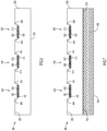
FIG. 1 illustrates a flowchart of a method for bonding multiple wafers together in accordance with the present invention. -
Fig. 2A illustrates a top view of a first wafer with a resist spun around a peripheral region of a top surface of the first wafer in accordance with the method illustrated inFIG. 1 . -
Fig. 2B illustrates a cross-sectional view of the first wafer illustrated inFIG. 2A , the cross-sectional view taken along line A-A inFIG. 2A . -
Fig. 3A illustrates a top view of the first wafer with pathways disposed in the resist in accordance with the method illustrated inFIG. 1 . -
Fig. 3B illustrates a cross-sectional view of the first wafer illustrated inFIG. 3A , the cross-sectional view taken along line B-B inFIG. 3A . -
FIG. 4 illustrates a cross-sectional view of the first wafer illustrated inFIGS. 2A, 2B ,3A, and 3B , where depressions are etched into the top surface of the first wafer through the pathways in accordance with the method illustrated inFIG. 1 . -
FIG. 5 illustrates a cross-sectional view of the first wafer illustrated inFIGS. 2A, 2B ,3A, and 3B , where adhesion metals are deposited onto the first wafer in accordance with the method illustrated inFIG. 1 . -
FIG. 6 illustrates a cross-sectional view of the first wafer illustrated inFIGS. 2A, 2B ,3A, and 3B , where the resist is removed from the first wafer in accordance with the method illustrated inFIG. 1 . -
FIG. 7 illustrates a cross-sectional view of the first wafer illustrated inFIGS. 2A, 2B ,3A, and 3B , where a second wafer is coupled to the bottom of the first wafer in accordance with the method illustrated inFIG. 1 . -
FIG. 8 illustrates a cross-sectional view of the first wafer illustrated inFIGS. 2A, 2B ,3A, and 3B , where indium is deposited on the first wafer in accordance with the method illustrated inFIG. 1 . -
FIG. 9 illustrates a cross-sectional view of the first wafer illustrated inFIGS. 2A, 2B ,3A, and 3B , where a third wafer is coupled to the top surface of the first wafer via the indium in accordance with the method illustrated inFIG. 1 . - Like reference numerals have been used to identify like elements throughout this disclosure.
- An exemplary method of wafer processing of a MEMS device utilized as image intensifiers of night vision goggles in accordance with the present invention are illustrated in
FIGS. 1 ,2A ,2B ,3A ,3B , and4-9 . Themethod 100 disclosed herein enables double sided wafer processing without damaging the adhesion metals to enable the formation of a low temperature hermetic seal with a reduced seal area. - As illustrated in
FIG. 1 , thefirst step 105 ofmethod 100 is to dispose a resist onto a region of a first side of a first wafer. Illustrated inFIGS. 2A and 2B is a region of afirst wafer 200 with a resist 210 being disposed or spun onto thefirst wafer 200 around the periphery of the region. Thefirst wafer 200 may be any type of wafer, including, but not limited to, a glass wafer, a silicon wafer, etc. Thefirst wafer 200 includes a first ortop side 202 and a second orbottom side 204. As illustrated inFIG. 2A , the region of thefirst wafer 200 is substantially rectangular in shape, but the first wafer may be of any other shape, including but not limited to, circular, pentagonal, octagonal, etc. - The resist 210 may be a photoresist that is disposed on the surface of the
first side 202 of thefirst wafer 200 by spin coating (e.g., a viscous, liquid solution of photoresist is dispensed onto thefirst wafer 200, and thefirst wafer 200 is spun rapidly to produce a uniformly thick layer). As best illustrated inFIG. 2A , the resist 210 may be disposed on the surface of thefirst side 202 of thefirst wafer 200 such that the resist 210 is disposed around the periphery of the region offirst wafer 200 proximate to theedges 206 of the region of thefirst wafer 200. Moreover, the resist 210 leaves acentral portion 208 of thefirst side 202 of thefirst wafer 200 exposed, which will later form a portion of a vacuum cavity when another wafer is bonded to thefirst wafer 200. The resist 210, when disposed on the surface of thefirst side 202 of thefirst wafer 200, may include a first ortop side 212 and a second orbottom side 214. Thesecond side 214 of the resist 210 is in abutment with thefirst side 202 of thefirst wafer 200. The proportions of the area of thefirst side 202 of the first wafer that is occupied by the resist 210 compared with thecentral portion 208, as illustrated inFIG. 2A , is for illustrative purposes only. Thus, thecentral portion 208 may occupy a larger area of thefirst wafer 200 than the resist 210. - Returning to
FIG. 1 , thesecond step 110 ofmethod 100 is to remove portions of the resist 210 to open pathways through the resist 210, where the pathways are the desired width of adhesion metals to later be deposited. Illustrated inFIGS. 3A and 3B a series ofpathways pathways first surface 212 to thesecond surface 214 to expose previously covered portions of the surface of thefirst side 202 of thefirst wafer 200. Moreover, thepathways first wafer 200 and thecentral portion 208 of thefirst wafer 200. Thefirst pathways 300 is the outermost pathway, thethird pathways 320 is the innermost pathway, and thesecond pathways 310 is disposed between the first andthird pathways pathways first wafer 200. - The
pathways pathways pathways - Turning back to
FIG. 1 , thethird step 115 ofmethod 100 is to etch depressions into the surface of thefirst side 202 of thefirst wafer 200 through thepathways first side 202 of thefirst wafer 200. As illustrated inFIG. 4 , a series ofdepressions first side 202 of thefirst wafer 200 such that each of thedepressions pathways first depression 400 is aligned with thefirst pathways 300, thesecond depression 410 is aligned with thesecond pathway 310, and thethird depression 420 is aligned with thethird pathway 320. Similar to thepathways depressions first wafer 200 and thecentral portion 208 of thefirst wafer 200. Thus, thefirst depression 400 is the outermost depression, thethird depression 420 is the innermost depression, and thesecond depression 410 is disposed between the first andthird depression depressions first side 202 of thefirst wafer 200 such that thedepressions central portion 208 of thefirst wafer 200. - As further illustrated in
FIG. 4 , each of thedepressions planar portion depressions first side 202 of thefirst wafer 200. In some embodiments, thedepressions first side 202 of thefirst wafer 200 such that eachdepression edges first side 202 of thefirst wafer 200 and theplanar portion FIG. 4 , thedepressions first side 202 of thefirst wafer 200 such that theedges depressions edges pathways depressions first side 202 of thefirst wafer 200 such that thedepressions - The surface of the
first side 202 of thefirst wafer 200 may be etched through thepathways depressions FIG. 4 , the etching may result in undercutting thepathways - Returning to
FIG. 1 , thefourth step 120 ofmethod 100 is to deposit adhesion metals to thefirst side 202 of thefirst wafer 200 outside of thecentral region 208. Thus, the adhesion metals are deposited over the resist 210, thepathways depressions central region 208 of thefirst wafer 200. In the embodiment illustrated inFIG. 5 , twoadhesion metals pathways adhesion metals depressions - As further illustrated in
FIG. 5 , thefirst adhesion metal 500 was first deposited such that thefirst adhesion metal 500 sits or rests on thefirst side 212 of the resist 210 and sits or rests directly on theplanar surfaces depressions second adhesion metal 510 is then deposited atop thefirst adhesion metal 500 such that thesecond adhesion metal 510 sits or rests on the deposits of thefirst adhesion metal 500 disposed on the resist 210 and the deposits of thefirst adhesion metal 500 disposed within thedepressions second adhesion metals planar surface depressions depressions depressions adhesion metals top side 202 of thefirst wafer 200. As illustrated, the resist 210 not only can be used to enable the formation of thedepressions adhesion metals first side 202 of thefirst wafer 200 outside of thedepressions - As previously explained, in the embodiment illustrated in
FIG. 5 , two adhesion metals are deposited onto thefirst wafer 200. In other embodiments, any number of adhesion metals may be deposited. Furthermore, any type of adhesion metal may be deposited, including, but not limited to, chromium, gold, nickel, titanium, etc. In the embodiment illustrated, thefirst adhesion metal 500 may be titanium and thesecond adhesion metal 510 may be gold. - Returning to
FIG. 1 , thefifth step 125 ofmethod 100 is to remove the resist 210 from thefirst side 202 of thefirst wafer 200. As illustrated inFIG. 6 , when the resist 210 is removed, the deposits of theadhesion metals first side 212 of the resist 210 are also removed. Thus, portions of thefirst side 202 of thefirst wafer 200 that were previously covered by the resist 210 are exposed. Furthermore, the only deposits of theadhesion metals first wafer 200 are the deposits of theadhesion metals depressions planar surface depressions adhesion metals first side 202 of thefirst wafer 200 outside of thedepressions - The
sixth step 130 ofmethod 100, as illustrated inFIG. 1 , is to bond a second wafer onto thesecond side 204 of thefirst wafer 200. As illustrated inFIG. 7 , asecond wafer 700 is bonded to thesecond side 204 of thefirst wafer 200. Thesecond wafer 700 may be any type of wafer, include, but not limited to, silicon, glass, etc. In the embodiment illustrated inFIG. 7 , however, thesecond wafer 700 is a silicon wafer. Thesecond wafer 700 may include afirst side 702 and asecond side 704. The surface of thefirst side 702 of thesecond wafer 700, as illustrated, is bonded, either directly or indirectly, to the surface of thesecond side 204 of thefirst wafer 200. The bonding of thesecond wafer 700 to thefirst wafer 200 may be any type of high temperature bond, which requires force to be applied to thefirst side 202 of thefirst wafer 200 and thesecond side 704 of thesecond wafer 700 during the bonding process. Thus, a tool is required to contact and apply force to thefirst side 202 of thefirst wafer 200 while simultaneously contacting and applying force to thesecond side 704 of thesecond wafer 700. Because theadhesion metals depressions first side 202 of thefirst wafer 200, and because theadhesion metals first side 202 of thefirst wafer 200, theadhesion metals second wafer 700 to thefirst wafer 200. Accordingly, application of the tool to thefirst side 202 of thefirst wafer 200 does not damage theadhesion metals - Turning back to
FIG. 1 , theseventh step 135 ofmethod 100 is to deposit indium onto theadhesion metals depressions FIG. 8 , when theindium adhesion metals depression indium indium depressions first side 202 of thefirst wafer 200. Moreover, each of theindium deposits FIG. 8 , are spaced from theedges depressions indium depressions indium first side 202 of thefirst wafer 200 like that of thedepressions depressions indium first wafer 200 and thecentral portion 208 of thefirst wafer 200. Thus, thefirst indium deposit 800 is the outermost indium deposit, thethird indium deposit 820 is the innermost indium deposit, and thesecond indium deposit 810 is disposed between the first andthird indium deposits indium deposits depressions - The
indium depressions adhesive metals indium indium depressions indium respective depression indium indium adhesion metals depressions FIG. 8 . In another embodiment, theindium depressions indium adhesion metals FIG. 8 . In yet another embodiment, theindium depression depression adhesion metals indium depressions indium - Returning to
FIG. 1 , once theindium final step 140 ofmethod 100 may be performed, which is to form a low temperature bond between a third wafer and thefirst side 202 of thefirst wafer 200. As illustrated inFIG. 9 , thethird wafer 900 may be any type of wafer, including, but not limited to, silicon, glass, etc. Furthermore, in the embodiment illustrated inFIG. 9 , thethird wafer 900 is a silicon wafer like that of thesecond wafer 700. Thethird wafer 900 may include afirst side 902 and asecond side 904. During the low temperature bonding process, thethird wafer 900 is pressed against thefirst wafer 200 such that thesecond side 904 of thethird wafer 900 is propelled or urged toward thefirst side 202 of thefirst wafer 200. As thethird wafer 900 is propelled toward thefirst wafer 200, thesecond side 904 of thethird wafer 900 comes into contact with the depositedindium third wafer 900 toward thefirst wafer 200 causes theindium first wafer 200 and thethird wafer 900. As illustrated inFIG. 9 , because of the shape of theindium deposits indium deposits indium deposits indium respective depressions respective edges depressions first side 202 of thefirst wafer 200. As further illustrated inFIG. 9 , theindium deposits gaps compressed indium deposits edges depressions compressed indium third wafer 900 and thefirst wafer 200. When thedepressions more edges indium deposits wafers - The method and structure described and illustrated provides a self-aligned method of making depressions and lithography mask for depositing adhesion metals onto a wafer such that the wafer can be processed without damaging the adhesion metals. This enables a first wafer to form a better and more guaranteed hermetic seal with a second wafer when using low temperature bonding processes. The described method also provides a structure that may cause multiple shear points in the flowing indium in order to provide a maximum bond surface for hermeticity. Multiple shear points may lead to the reduction in the number of bond lines (i.e., depressions), which thereby reduce the overall seal line width enabling more die per wafer.
- It is to be understood that terms such as "left," "right," "top," "bottom," "front," "rear," "side," "height," "length," "width," "upper," "lower," "interior," "exterior," "inner," "outer" and the like as may be used herein, merely describe points or portions of reference and do not limit the present invention to any particular orientation or configuration. Further, the term "exemplary" is used herein to describe an example or illustration. Any embodiment described herein as exemplary is not to be construed as a preferred or advantageous embodiment, but rather as one example or illustration of a possible embodiment of the invention.
- Although the disclosed inventions are illustrated and described herein as embodied in one or more specific examples, it is nevertheless not intended to be limited to the details shown, since various modifications and structural changes may be made therein without departing from the scope of the inventions and within the scope and range of equivalents of the claims. In addition, various features from one of the embodiments may be incorporated into another of the embodiments. Accordingly, it is appropriate that the appended claims be construed broadly and in a manner consistent with the scope of the disclosure as set forth in the following claims.
Claims (10)
- A method for forming a low temperature bond between wafers, the method comprising:spinning a resist onto a first side of a first wafer;forming one or more pathways within the resist to expose portions of the first side of the first wafer;etching the first side of the first wafer through the one or more pathways to form one or more depressions that align with the pathways, each of the one or more depressions having a planar surface and edges;depositing one or more adhesion metals over the resist such that the one or more adhesion metals is deposited within each of the one or more depressions;removing the resist;depositing indium onto the one or more adhesion metals deposited within the one or more depressions;compressing the indium between a second wafer and the first side of the first wafer to form a low temperature bond between the second wafer and the first wafer.
- The method of claim 1, wherein the one or more depressions are concentric to the first wafer.
- The method of claim 1, wherein each of the one or more depressions extend continuously around a peripheral region of the first side of the first wafer.
- The method of claim 1, wherein the one or more adhesion metals comprise:a first adhesion metal of titanium; anda second adhesion metal of gold.
- The method of claim 1, wherein the edges of the one or more depressions form shear points for the indium when the indium is compressed.
- The method of claim 1, further comprising, prior to depositing the indium:bonding a third wafer to a second surface of the first wafer.
- The method of claim 6, wherein the bond between the second wafer and the first side of the first wafer is a hermetic bond, and the bonding of the third wafer of the first wafer is a high temperature bond.
- The method of claim 6, wherein the second and third wafers are silicon wafers.
- The method of claim 1, wherein the first wafer is a glass wafer.
- The method of claim 1, wherein the one or more depressions are etched into the first side of the first wafer via isotropic etching.
Applications Claiming Priority (1)
| Application Number | Priority Date | Filing Date | Title |
|---|---|---|---|
| US15/829,314 US10584027B2 (en) | 2017-12-01 | 2017-12-01 | Method for forming hermetic seals in MEMS devices |
Publications (2)
| Publication Number | Publication Date |
|---|---|
| EP3492423A1 true EP3492423A1 (en) | 2019-06-05 |
| EP3492423B1 EP3492423B1 (en) | 2026-06-03 |
Family
ID=64456761
Family Applications (1)
| Application Number | Title | Priority Date | Filing Date |
|---|---|---|---|
| EP18207750.3A Active EP3492423B1 (en) | 2017-12-01 | 2018-11-22 | Method for forming hermetic seals in mems devices |
Country Status (3)
| Country | Link |
|---|---|
| US (2) | US10584027B2 (en) |
| EP (1) | EP3492423B1 (en) |
| JP (1) | JP7281894B2 (en) |
Cited By (1)
| Publication number | Priority date | Publication date | Assignee | Title |
|---|---|---|---|---|
| US11174151B2 (en) | 2019-11-19 | 2021-11-16 | Invensense, Inc. | Integrated MEMS cavity seal |
Families Citing this family (1)
| Publication number | Priority date | Publication date | Assignee | Title |
|---|---|---|---|---|
| US20210340007A1 (en) * | 2020-04-29 | 2021-11-04 | Elbit Systems Of America, Llc | Mems hermetic seal apparatus and methods |
Citations (4)
| Publication number | Priority date | Publication date | Assignee | Title |
|---|---|---|---|---|
| US5723945A (en) * | 1996-04-09 | 1998-03-03 | Electro Plasma, Inc. | Flat-panel display |
| WO1999003122A1 (en) * | 1997-07-11 | 1999-01-21 | Fed Corporation | Anhydrous method of packaging organic light emitting displays |
| US20050082480A1 (en) * | 2003-08-26 | 2005-04-21 | Aegis Semiconductor, Inc. | Infrared camera system |
| US20130175084A1 (en) * | 2012-01-09 | 2013-07-11 | Sri Hermetics Inc. | Electronic device including indium gasket and related methods |
Family Cites Families (25)
| Publication number | Priority date | Publication date | Assignee | Title |
|---|---|---|---|---|
| US5197653A (en) | 1992-03-27 | 1993-03-30 | Honeywell Inc. | Method of sealing two articles together with an indium preform seal |
| US5940694A (en) * | 1996-07-22 | 1999-08-17 | Bozada; Christopher A. | Field effect transistor process with semiconductor mask, single layer integrated metal, and dual etch stops |
| US6507147B1 (en) | 2000-08-31 | 2003-01-14 | Intevac, Inc. | Unitary vacuum tube incorporating high voltage isolation |
| US6605519B2 (en) * | 2001-05-02 | 2003-08-12 | Unaxis Usa, Inc. | Method for thin film lift-off processes using lateral extended etching masks and device |
| US7253091B2 (en) * | 2001-09-28 | 2007-08-07 | Hrl Laboratories, Llc | Process for assembling three-dimensional systems on a chip and structure thus obtained |
| US6962835B2 (en) * | 2003-02-07 | 2005-11-08 | Ziptronix, Inc. | Method for room temperature metal direct bonding |
| JP3823981B2 (en) * | 2003-05-12 | 2006-09-20 | セイコーエプソン株式会社 | PATTERN AND WIRING PATTERN FORMING METHOD, DEVICE AND ITS MANUFACTURING METHOD, ELECTRO-OPTICAL DEVICE, ELECTRONIC DEVICE, AND ACTIVE MATRIX SUBSTRATE MANUFACTURING METHOD |
| JP4489393B2 (en) | 2003-08-21 | 2010-06-23 | オリンパス株式会社 | Semiconductor device |
| US7607560B2 (en) | 2004-05-14 | 2009-10-27 | Intevac, Inc. | Semiconductor die attachment for high vacuum tubes |
| US20090115042A1 (en) * | 2004-06-04 | 2009-05-07 | Zycube Co., Ltd. | Semiconductor device having three-dimensional stacked structure and method of fabricating the same |
| SG191562A1 (en) | 2004-11-04 | 2013-07-31 | Microchips Inc | Compression cold welding process for forming vias |
| US7442570B2 (en) * | 2005-03-18 | 2008-10-28 | Invensence Inc. | Method of fabrication of a AL/GE bonding in a wafer packaging environment and a product produced therefrom |
| JP4551255B2 (en) * | 2005-03-31 | 2010-09-22 | ルネサスエレクトロニクス株式会社 | Semiconductor device |
| DK1962344T3 (en) * | 2007-02-25 | 2012-07-02 | Samsung Electronics Co Ltd | Packaging for electronic devices and manufacturing processes |
| JP5159273B2 (en) * | 2007-11-28 | 2013-03-06 | ルネサスエレクトロニクス株式会社 | Manufacturing method of electronic device |
| JP5592072B2 (en) | 2009-01-22 | 2014-09-17 | 曙ブレーキ工業株式会社 | Processing equipment |
| US11134598B2 (en) | 2009-07-20 | 2021-09-28 | Set North America, Llc | 3D packaging with low-force thermocompression bonding of oxidizable materials |
| US8486744B2 (en) | 2010-09-28 | 2013-07-16 | Taiwan Semiconductor Manufacturing Company, Ltd. | Multiple bonding in wafer level packaging |
| US8912017B2 (en) * | 2011-05-10 | 2014-12-16 | Ostendo Technologies, Inc. | Semiconductor wafer bonding incorporating electrical and optical interconnects |
| SG11201402261SA (en) * | 2011-12-07 | 2014-08-28 | Georgia Tech Res Inst | Packaging compatible wafer level capping of mems devices |
| US8686571B2 (en) * | 2012-08-09 | 2014-04-01 | Taiwan Semiconductor Manufacturing Company, Ltd. | Bonding layer structure and method for wafer to wafer bonding |
| CN102786026B (en) | 2012-08-23 | 2015-04-22 | 江苏物联网研究发展中心 | Film sealing cap packaging structure for MEMS optical device and manufacturing method thereof |
| KR20150101875A (en) * | 2014-02-27 | 2015-09-04 | 삼성전자주식회사 | Method of forming fine pattern using block copolymers |
| US10266395B2 (en) | 2015-08-21 | 2019-04-23 | Taiwan Semiconductor Manufacturing Company Ltd. | Semiconductive structure and manufacturing method thereof |
| US9852988B2 (en) * | 2015-12-18 | 2017-12-26 | Invensas Bonding Technologies, Inc. | Increased contact alignment tolerance for direct bonding |
-
2017
- 2017-12-01 US US15/829,314 patent/US10584027B2/en active Active
-
2018
- 2018-11-22 EP EP18207750.3A patent/EP3492423B1/en active Active
- 2018-11-30 JP JP2018224625A patent/JP7281894B2/en active Active
-
2020
- 2020-01-27 US US16/773,042 patent/US11161737B2/en active Active
Patent Citations (4)
| Publication number | Priority date | Publication date | Assignee | Title |
|---|---|---|---|---|
| US5723945A (en) * | 1996-04-09 | 1998-03-03 | Electro Plasma, Inc. | Flat-panel display |
| WO1999003122A1 (en) * | 1997-07-11 | 1999-01-21 | Fed Corporation | Anhydrous method of packaging organic light emitting displays |
| US20050082480A1 (en) * | 2003-08-26 | 2005-04-21 | Aegis Semiconductor, Inc. | Infrared camera system |
| US20130175084A1 (en) * | 2012-01-09 | 2013-07-11 | Sri Hermetics Inc. | Electronic device including indium gasket and related methods |
Cited By (1)
| Publication number | Priority date | Publication date | Assignee | Title |
|---|---|---|---|---|
| US11174151B2 (en) | 2019-11-19 | 2021-11-16 | Invensense, Inc. | Integrated MEMS cavity seal |
Also Published As
| Publication number | Publication date |
|---|---|
| US20190169023A1 (en) | 2019-06-06 |
| US10584027B2 (en) | 2020-03-10 |
| US11161737B2 (en) | 2021-11-02 |
| US20200156932A1 (en) | 2020-05-21 |
| EP3492423B1 (en) | 2026-06-03 |
| JP2019098516A (en) | 2019-06-24 |
| JP7281894B2 (en) | 2023-05-26 |
Similar Documents
| Publication | Publication Date | Title |
|---|---|---|
| US20180277763A1 (en) | Method for producing vapor deposition mask, and method for producing organic semiconductor element | |
| JP4083841B2 (en) | Semiconductor device packaging method | |
| US11414320B2 (en) | Methods for producing thin-film layers and microsystems having thin-film layers | |
| JPH04129267A (en) | Semiconductor substrate and manufacture thereof | |
| US20100002894A1 (en) | MEMS device and method of making the same | |
| CN102786026B (en) | Film sealing cap packaging structure for MEMS optical device and manufacturing method thereof | |
| US11161737B2 (en) | Method for forming hermetic seals in MEMS devices | |
| JP6301565B1 (en) | Method and apparatus for separating a microchip from a wafer and mounting the microchip on a substrate | |
| US20060237810A1 (en) | Bonding interface for micro-device packaging | |
| EP3041784A1 (en) | Method of forming deposited patterns on a surface | |
| JPH10128633A (en) | Vacuum suction device | |
| TWI772485B (en) | Micromechanical device and corresponding production method | |
| CN117219580A (en) | Chip separation method | |
| US7652384B2 (en) | Fabricating tall micro structures | |
| US20070090479A1 (en) | Controlling bond fronts in wafer-scale packaging | |
| US8926848B2 (en) | Through hole forming method | |
| JP2025521952A (en) | METHOD OF MANUFACTURING METAL MICROSTRUCTURES AND SEMICONDUCTOR DEVICES | |
| KR20040058085A (en) | Stencil mask and manufacturing method thereof | |
| CN111099555B (en) | A glass cavity manufacturing method suitable for wafer-level vacuum packaging | |
| CN110161809B (en) | Structure and method for improving adhesiveness of photoresist | |
| US20250218847A1 (en) | Configurable carrier for transfer and self-assembly of multiple integrated circuit devices | |
| CN102082070B (en) | Method for protecting metal layer in process of thinning wafer | |
| RU2848152C1 (en) | Method for manufacturing a sensitive element of an accelerometer | |
| CN112624034A (en) | Wafer-level packaging method and packaging structure of MEMS (micro-electromechanical systems) device | |
| US20250132158A1 (en) | Use of tin thin film for bonding and as masking film |
Legal Events
| Date | Code | Title | Description |
|---|---|---|---|
| PUAI | Public reference made under article 153(3) epc to a published international application that has entered the european phase |
Free format text: ORIGINAL CODE: 0009012 |
|
| STAA | Information on the status of an ep patent application or granted ep patent |
Free format text: STATUS: REQUEST FOR EXAMINATION WAS MADE |
|
| 17P | Request for examination filed |
Effective date: 20181122 |
|
| AK | Designated contracting states |
Kind code of ref document: A1 Designated state(s): AL AT BE BG CH CY CZ DE DK EE ES FI FR GB GR HR HU IE IS IT LI LT LU LV MC MK MT NL NO PL PT RO RS SE SI SK SM TR |
|
| AX | Request for extension of the european patent |
Extension state: BA ME |
|
| STAA | Information on the status of an ep patent application or granted ep patent |
Free format text: STATUS: EXAMINATION IS IN PROGRESS |
|
| 17Q | First examination report despatched |
Effective date: 20210903 |
|
| 17Q | First examination report despatched |
Effective date: 20211006 |
|
| RAP1 | Party data changed (applicant data changed or rights of an application transferred) |
Owner name: ELBIT SYSTEMS OF AMERICA, LLC |
|
| GRAP | Despatch of communication of intention to grant a patent |
Free format text: ORIGINAL CODE: EPIDOSNIGR1 |
|
| STAA | Information on the status of an ep patent application or granted ep patent |
Free format text: STATUS: GRANT OF PATENT IS INTENDED |
|
| INTG | Intention to grant announced |
Effective date: 20230511 |
|
| P01 | Opt-out of the competence of the unified patent court (upc) registered |
Effective date: 20230602 |
|
| GRAJ | Information related to disapproval of communication of intention to grant by the applicant or resumption of examination proceedings by the epo deleted |
Free format text: ORIGINAL CODE: EPIDOSDIGR1 |
|
| STAA | Information on the status of an ep patent application or granted ep patent |
Free format text: STATUS: EXAMINATION IS IN PROGRESS |
|
| INTC | Intention to grant announced (deleted) | ||
| GRAP | Despatch of communication of intention to grant a patent |
Free format text: ORIGINAL CODE: EPIDOSNIGR1 |
|
| STAA | Information on the status of an ep patent application or granted ep patent |
Free format text: STATUS: GRANT OF PATENT IS INTENDED |
|
| INTG | Intention to grant announced |
Effective date: 20251120 |
|
| GRAJ | Information related to disapproval of communication of intention to grant by the applicant or resumption of examination proceedings by the epo deleted |
Free format text: ORIGINAL CODE: EPIDOSDIGR1 |
|
| STAA | Information on the status of an ep patent application or granted ep patent |
Free format text: STATUS: EXAMINATION IS IN PROGRESS |
|
| INTC | Intention to grant announced (deleted) | ||
| GRAP | Despatch of communication of intention to grant a patent |
Free format text: ORIGINAL CODE: EPIDOSNIGR1 |
|
| STAA | Information on the status of an ep patent application or granted ep patent |
Free format text: STATUS: GRANT OF PATENT IS INTENDED |
|
| INTG | Intention to grant announced |
Effective date: 20260324 |
|
| GRAS | Grant fee paid |
Free format text: ORIGINAL CODE: EPIDOSNIGR3 |
|
| GRAA | (expected) grant |
Free format text: ORIGINAL CODE: 0009210 |
|
| STAA | Information on the status of an ep patent application or granted ep patent |
Free format text: STATUS: THE PATENT HAS BEEN GRANTED |
|
| AK | Designated contracting states |
Kind code of ref document: B1 Designated state(s): AL AT BE BG CH CY CZ DE DK EE ES FI FR GB GR HR HU IE IS IT LI LT LU LV MC MK MT NL NO PL PT RO RS SE SI SK SM TR |
|
| REG | Reference to a national code |
Ref country code: CH Ref legal event code: F10 Free format text: ST27 STATUS EVENT CODE: U-0-0-F10-F00 (AS PROVIDED BY THE NATIONAL OFFICE) Effective date: 20260603 Ref country code: GB Ref legal event code: FG4D |
|
| REG | Reference to a national code |
Ref country code: DE Ref legal event code: R096 Ref document number: 602018091621 Country of ref document: DE |
|
| REG | Reference to a national code |
Ref country code: IE Ref legal event code: FG4D |