EP3492211A1 - Laser treatment method, bonding method, copper member, method for manufacturing multilayer print wiring substrate, and multilayer print wiring substrate - Google Patents
Laser treatment method, bonding method, copper member, method for manufacturing multilayer print wiring substrate, and multilayer print wiring substrate Download PDFInfo
- Publication number
- EP3492211A1 EP3492211A1 EP17834394.3A EP17834394A EP3492211A1 EP 3492211 A1 EP3492211 A1 EP 3492211A1 EP 17834394 A EP17834394 A EP 17834394A EP 3492211 A1 EP3492211 A1 EP 3492211A1
- Authority
- EP
- European Patent Office
- Prior art keywords
- copper
- laser
- periodic structure
- pulse
- pulse width
- Prior art date
- Legal status (The legal status is an assumption and is not a legal conclusion. Google has not performed a legal analysis and makes no representation as to the accuracy of the status listed.)
- Withdrawn
Links
Images


Classifications
-
- B—PERFORMING OPERATIONS; TRANSPORTING
- B23—MACHINE TOOLS; METAL-WORKING NOT OTHERWISE PROVIDED FOR
- B23K—SOLDERING OR UNSOLDERING; WELDING; CLADDING OR PLATING BY SOLDERING OR WELDING; CUTTING BY APPLYING HEAT LOCALLY, e.g. FLAME CUTTING; WORKING BY LASER BEAM
- B23K26/00—Working by laser beam, e.g. welding, cutting or boring
- B23K26/02—Positioning or observing the workpiece, e.g. with respect to the point of impact; Aligning, aiming or focusing the laser beam
- B23K26/06—Shaping the laser beam, e.g. by masks or multi-focusing
- B23K26/062—Shaping the laser beam, e.g. by masks or multi-focusing by direct control of the laser beam
- B23K26/0626—Energy control of the laser beam
-
- H—ELECTRICITY
- H05—ELECTRIC TECHNIQUES NOT OTHERWISE PROVIDED FOR
- H05K—PRINTED CIRCUITS; CASINGS OR CONSTRUCTIONAL DETAILS OF ELECTRIC APPARATUS; MANUFACTURE OF ASSEMBLAGES OF ELECTRICAL COMPONENTS
- H05K3/00—Apparatus or processes for manufacturing printed circuits
- H05K3/46—Manufacturing multilayer circuits
- H05K3/4644—Manufacturing multilayer circuits by building the multilayer layer by layer, i.e. build-up multilayer circuits
- H05K3/4652—Adding a circuit layer by laminating a metal foil or a preformed metal foil pattern
-
- B—PERFORMING OPERATIONS; TRANSPORTING
- B23—MACHINE TOOLS; METAL-WORKING NOT OTHERWISE PROVIDED FOR
- B23K—SOLDERING OR UNSOLDERING; WELDING; CLADDING OR PLATING BY SOLDERING OR WELDING; CUTTING BY APPLYING HEAT LOCALLY, e.g. FLAME CUTTING; WORKING BY LASER BEAM
- B23K26/00—Working by laser beam, e.g. welding, cutting or boring
- B23K26/352—Working by laser beam, e.g. welding, cutting or boring for surface treatment
- B23K26/354—Working by laser beam, e.g. welding, cutting or boring for surface treatment by melting
-
- B—PERFORMING OPERATIONS; TRANSPORTING
- B23—MACHINE TOOLS; METAL-WORKING NOT OTHERWISE PROVIDED FOR
- B23K—SOLDERING OR UNSOLDERING; WELDING; CLADDING OR PLATING BY SOLDERING OR WELDING; CUTTING BY APPLYING HEAT LOCALLY, e.g. FLAME CUTTING; WORKING BY LASER BEAM
- B23K26/00—Working by laser beam, e.g. welding, cutting or boring
- B23K26/36—Removing material
- B23K26/362—Laser etching
- B23K26/364—Laser etching for making a groove or trench, e.g. for scribing a break initiation groove
-
- C—CHEMISTRY; METALLURGY
- C23—COATING METALLIC MATERIAL; COATING MATERIAL WITH METALLIC MATERIAL; CHEMICAL SURFACE TREATMENT; DIFFUSION TREATMENT OF METALLIC MATERIAL; COATING BY VACUUM EVAPORATION, BY SPUTTERING, BY ION IMPLANTATION OR BY CHEMICAL VAPOUR DEPOSITION, IN GENERAL; INHIBITING CORROSION OF METALLIC MATERIAL OR INCRUSTATION IN GENERAL
- C23C—COATING METALLIC MATERIAL; COATING MATERIAL WITH METALLIC MATERIAL; SURFACE TREATMENT OF METALLIC MATERIAL BY DIFFUSION INTO THE SURFACE, BY CHEMICAL CONVERSION OR SUBSTITUTION; COATING BY VACUUM EVAPORATION, BY SPUTTERING, BY ION IMPLANTATION OR BY CHEMICAL VAPOUR DEPOSITION, IN GENERAL
- C23C26/00—Coating not provided for in groups C23C2/00 - C23C24/00
-
- H—ELECTRICITY
- H05—ELECTRIC TECHNIQUES NOT OTHERWISE PROVIDED FOR
- H05K—PRINTED CIRCUITS; CASINGS OR CONSTRUCTIONAL DETAILS OF ELECTRIC APPARATUS; MANUFACTURE OF ASSEMBLAGES OF ELECTRICAL COMPONENTS
- H05K3/00—Apparatus or processes for manufacturing printed circuits
-
- H—ELECTRICITY
- H05—ELECTRIC TECHNIQUES NOT OTHERWISE PROVIDED FOR
- H05K—PRINTED CIRCUITS; CASINGS OR CONSTRUCTIONAL DETAILS OF ELECTRIC APPARATUS; MANUFACTURE OF ASSEMBLAGES OF ELECTRICAL COMPONENTS
- H05K3/00—Apparatus or processes for manufacturing printed circuits
- H05K3/38—Improvement of the adhesion between the insulating substrate and the metal
-
- B—PERFORMING OPERATIONS; TRANSPORTING
- B23—MACHINE TOOLS; METAL-WORKING NOT OTHERWISE PROVIDED FOR
- B23K—SOLDERING OR UNSOLDERING; WELDING; CLADDING OR PLATING BY SOLDERING OR WELDING; CUTTING BY APPLYING HEAT LOCALLY, e.g. FLAME CUTTING; WORKING BY LASER BEAM
- B23K2101/00—Articles made by soldering, welding or cutting
- B23K2101/36—Electric or electronic devices
- B23K2101/42—Printed circuits
-
- B—PERFORMING OPERATIONS; TRANSPORTING
- B23—MACHINE TOOLS; METAL-WORKING NOT OTHERWISE PROVIDED FOR
- B23K—SOLDERING OR UNSOLDERING; WELDING; CLADDING OR PLATING BY SOLDERING OR WELDING; CUTTING BY APPLYING HEAT LOCALLY, e.g. FLAME CUTTING; WORKING BY LASER BEAM
- B23K2103/00—Materials to be soldered, welded or cut
- B23K2103/08—Non-ferrous metals or alloys
- B23K2103/12—Copper or alloys thereof
-
- B—PERFORMING OPERATIONS; TRANSPORTING
- B23—MACHINE TOOLS; METAL-WORKING NOT OTHERWISE PROVIDED FOR
- B23K—SOLDERING OR UNSOLDERING; WELDING; CLADDING OR PLATING BY SOLDERING OR WELDING; CUTTING BY APPLYING HEAT LOCALLY, e.g. FLAME CUTTING; WORKING BY LASER BEAM
- B23K2103/00—Materials to be soldered, welded or cut
- B23K2103/16—Composite materials
- B23K2103/166—Multilayered materials
Definitions
- the present invention relates to a laser processing method of processing a copper surface by using laser, a joint method of joining copper foil to a resin material, and a copper member provided with surface processing.
- Patent Literatures 1 to 3 disclose technologies of roughing the surface of a metal member to form irregularity at a joint with a dissimilar material, in particular, thereby increasing adhesion at the joint.
- the surface of a metal member is roughed to form irregularity at a joint with a dissimilar material.
- finer irregularity is desired to be formed on the copper surface to increase adhesion with a resin material while reducing a transmission loss due to the skin effect.
- Patent Literatures 1 to 3 it is difficult to apply the inventions according to Patent Literatures 1 to 3 to form fine irregularity on the surface of metal such as copper having significantly high thermal conductivity and low light absorptivity. Specifically, it needs to use ultrashort pulse laser of picoseconds or femtoseconds to form fine irregularity on the surface, but such ultrashort pulse laser has low processing efficiency due to the short duration of mutual interaction between light and metal, and laser itself is also expensive.
- an object of the present invention is to provide a laser processing method capable of processing a copper surface to have a favorable electric characteristic and desirable adhesion with a resin material, a joint method of joining copper foil to a resin material, a copper member provided with surface processing, a method of manufacturing a multi-layer printed circuit board, and a multi-layer printed circuit board.
- a laser processing method is a laser processing method of performing surface processing on a copper surface by using laser.
- the method is characterized by forming a periodic structure on the order of laser wavelength on the copper surface by irradiating the copper surface with pulse laser having a laser power close to a threshold beyond which copper processing is possible and having a pulse width on the order of nanoseconds.
- the method manages the pulse width on the order of nanoseconds in a high fluence region, which has not been conventionally discussed, and forms a periodic structure on the order of laser wavelength on the copper surface.
- the fluence is a value obtained by dividing the peak power of the pulse laser by the beam area.
- a periodic structure on the order of laser wavelength can be formed on a copper surface by irradiating the copper surface with pulse laser having a laser power close to a threshold beyond which copper processing is possible and having a pulse width on the order of nanoseconds.
- a periodic structure on the order of laser wavelength a high-frequency signal can be transmitted at low loss, and the periodic structure functions as an anchor when joined with another member to have favorable adhesion with the member.
- fast and inexpensively processing can be achieved as compared to, for example, a case of using ultrashort pulse laser of picoseconds or femtoseconds.
- the laser processing method according to a preferable aspect of the present invention is characterized by forming a coating on the copper surface together with forming the periodic structure on the order of laser wavelength on the copper surface.
- the laser processing method is characterized by forming a dendrite structure having a period shorter than a period of the periodic structure on the order of laser wavelength by accumulating or depositing copper at a protruding part of the periodic structure on the order of laser wavelength.
- the laser processing method is characterized in that the copper surface is irradiated with pulse laser having a wavelength of 1000 nm to 1600 nm, a pulse width of 0.8 ns to 5.0 ns, and a fluence of 1.0 ⁇ 10 8 W/cm 2 to 4.0 ⁇ 10 9 W/cm 2 under air or atmosphere of oxygen, water, or active gas.
- the laser processing method is characterized in that the periodic structure is formed in a predetermined direction on the copper surface by irradiating the copper surface with the pulse laser while controlling the polarization direction of the pulse laser.
- anisotropic adhesion control to obtain strong adhesion in the predetermined direction and weak adhesion in a direction orthogonal to the predetermined direction can be achieved.
- the laser processing method is characterized in that the copper surface is irradiated with the pulse laser having an energy profile set in a top hat shape.
- the laser processing method is characterized in that an identical irradiation position on the copper surface is irradiated with the pulse laser while the fluence of the pulse laser is gradually reduced.
- a joint method is a joint method of joining copper foil to a resin material.
- the method is characterized by forming a roughed part having a periodic structure on the order of laser wavelength on a surface of the copper foil by irradiating the surface of the copper foil with pulse laser having a laser power close to a threshold beyond which copper processing is possible and having a pulse width on the order of nanoseconds, and performs laser welding or heat press bonding of the roughed part formed on the surface of the copper foil to the resin material.
- a periodic structure having a period of 0.35 ⁇ m to 2 ⁇ m in a planar direction and a height of less than 1.5 ⁇ m is formed on at least one surface.
- the copper member according to a preferable aspect of the present invention is characterized in that the ratio of the height of the periodic structure relative to the thickness of the copper member is 0.15% to 30% inclusive.
- the copper member according to a preferable aspect of the present invention is characterized in that a coating is formed on the periodic structure, and an irregular structure having a period shorter than a period of the periodic structure is formed on a surface of the coating.
- the copper member according to a preferable aspect of the present invention is characterized in that the surface area of the coating on which the irregular structure is formed is at least ten times larger than the surface area of the surface on which the periodic structure is formed.
- the copper member according to a preferable aspect of the present invention is characterized in that the irregular structure is made of a dendrite structure.
- the copper member according to a preferable aspect of the present invention is characterized in that the copper member is copper foil.
- a method of manufacturing a printed circuit board according to one aspect of the present invention is a printed circuit board manufacturing method of manufacturing a multi-layer printed circuit board.
- the method is characterized by forming a periodic structure on the order of laser wavelength at the inner-layer wiring part by selectively irradiating an inner-layer wiring part of the multi-layer printed circuit board with pulse laser having a laser power close to a threshold beyond which copper processing is possible and having a pulse width on the order of nanoseconds.
- the method of manufacturing a printed circuit board according to a preferable aspect of the present invention provides a multi-layer printed circuit board on which an inner-layer wiring part is formed, characterized in that a periodic structure having a period of 0.35 ⁇ m to 2 ⁇ m in a planar direction and a height of less than 1.5 ⁇ m is formed in parallel to a current conduction direction at the inner-layer wiring part.
- the present invention can provide a laser processing method capable of processing a copper surface to have a favorable electric characteristic and desirable adhesion with a resin material, a joint method of joining copper foil to a resin material, a copper member provided with surface processing, a method of manufacturing a multi-layer printed circuit board, and a multi-layer printed circuit board.
- the present embodiment relates to a laser processing method of performing surface processing on a copper surface by using laser.
- Fig. 1 is a diagram schematically illustrating a laser processing process of performing surface processing on a copper surface by using laser.
- a copper surface 11 of a copper member 10 is irradiated with pulse laser having a pulse width managed on the order of nanoseconds in a high fluence region, which has not been conventionally discussed.
- the copper surface 11 of the copper member 10 is irradiated with pulse laser 2 having a laser power close to a threshold beyond which copper processing is possible and having a pulse width on the order of nanoseconds.
- the order of nanoseconds indicates, for example, the range of 0.8 ns to 5.0 ns.
- the fluence is a value obtained by dividing the peak power of the pulse laser by the beam area.
- the copper member 10 is made of a metallic material containing copper (Cu) as a primary component, and is, for example, a copper plate. In the present embodiment, such a copper plate having a thickness of 500 ⁇ m or lessis referred to as copper foil. In the present embodiment, as an example, the copper member 10 is copper foil, and referred to as "copper foil 10" below.
- Fig. 2 is a diagram illustrating evaluation of surface processing in which laser processing is performed under a plurality of kinds of conditions into four items of "processing", “mixed processing and coating removal”, “coating removal”, and “blackening” where the horizontal axis represents the pulse width [ns] and the vertical axis represents fluence [W/cm 2 ].
- the “processing” refers to a processing in which copper is removed through melting and evaporation due to ablation or heat input to form a groove in a size equivalent to the diameter of a processing beam
- the “coating removal” refers to processing in which only a copper compound coating such as rust on the copper foil surface is removed
- the “mixed processing and coating removal” refers to processing in which the processing and the coating removal are simultaneously performed
- the “blackening” refers to processing in a middle region between the “processing” and the “coating removal”, in which a coating of oxide or the like on the copper foil surface and a fine periodic structure on the order of laser wavelength are simultaneously formed.
- the beam diameter refers to the spot size of a Gaussian beam.
- the processing beam When the processing is performed with the Gaussian beam, a copper surface layer is removed at a central part of the beam, at which the fluence is high, in the blackening in some cases.
- the processing beam has an energy profile in a top hat shape than a Gaussian shape. Accordingly, it is preferable to set the energy profile of the pulse laser in a top hat shape.
- the evaluation illustrated in Fig. 2 indicates it is preferable to perform processing at a fluence and a pulse width between the "processing" and the "coating removal". Specifically, a laser processing condition of a pulse width (first pulse width) and a fluence (first fluence) with which formation of a groove in a size equivalent to the processing beam diameter on the copper surface 11 is possible, and a laser processing condition of a pulse width (second pulse) and a fluence (second fluence) that have values smaller than the values of the first pulse width and the first fluence, respectively and with which removal of only a copper compound coating from the copper surface 11 is possible are acquired and stored as profile data in advance in, for example, a storage provided to a laser processing apparatus.
- the laser processing apparatus forms a periodic structure on the order of laser wavelength by referring to the profile data and irradiating the copper surface 11 with pulse laser having a pulse width set to be between the first pulse width and the second pulse width and a fluence set to be between the first fluence and the second fluence.
- pulse laser set to have a pulse width of 0.8 ns to 5.0 ns and a fluence of 1.0 ⁇ 10 8 W/cm 2 to 4.0 ⁇ 10 9 W/cm 2 , which are specific numerical values obtained from the result illustrated in Fig. 2 , is used
- pulse energy is close to a processing threshold of the copper foil, and a periodic structure 12 and a coating 13 can be formed on the copper surface 11 of the copper foil 10 as illustrated in Fig. 1 .
- pulse laser having a laser power close to a threshold beyond which copper processing is possible and having a pulse width on the order of nanoseconds satisfy conditions as follows.
- the pulse width on the order of nanoseconds has a range of 0.8 ns to 999 ns.
- pulse laser having a wavelength of 1000 nm to 1600 nm, a pulse width of 0.8 ns to 999 ns, and a fluence of 1.0 ⁇ 10 8 W/cm 2 to 4.0 ⁇ 10 9 W/cm 2 in air under atmosphere of oxygen, water, or active gas.
- the copper surface 11 be irradiated with pulse laser having a wavelength of 1000 nm to 1600 nm, a pulse width of 0.8 ns to 5.0 ns, and a fluence of 1.0 ⁇ 10 8 W/cm 2 to 4.0 ⁇ 10 9 W/cm 2 under air or atmosphere of oxygen, water, or active gas.
- the copper surface 11 be irradiated with pulse laser having a wavelength of 1000 nm to 1600 nm, a pulse width of 1.0 ns to 5.0 ns, and a fluence of 1.0 ⁇ 10 8 W/cm 2 to 4.0 ⁇ 10 9 W/cm 2 under air or atmosphere of oxygen, water, or active gas.
- Copper causes improvement of light absorptivity and decrease of thermal conductivity when an oxide coating is formed on the surface thereof, and laser processing is promoted accordingly.
- the processing be performed while the fluence is gradually reduced.
- the periodic structure is formed orthogonal to the polarization direction of a processing beam.
- a structure having periodicity in an optional direction can be formed by irradiating the copper surface 11 with pulse laser while controlling the polarization direction of the pulse laser through a wave plate or the like.
- Anisotropic adhesion control to obtain strong adhesion in the predetermined direction and weak adhesion in a direction orthogonal to the predetermined direction can be achieved by forming the periodic structure in the predetermined direction in this manner.
- the periodic structure 12 and the coating 13 on the order of wavelength can be formed on the copper surface 11 of the copper foil 10 by appropriately controlling the fluence so that the laser power becomes close to the threshold beyond which copper processing is possible as described above.
- the order of wavelength has, for example, a range of 1000 nm to 1600 nm.
- a periodic structure of 1000 nm or less may be formed by shortening the laser wavelength.
- pulse laser having at least one of parameters of frequency, laser intensity, scanning speed, spot size, wavelength, and atmosphere adjusted in accordance with the height and shape of the periodic structure 12 to be formed on the copper surface 11.
- the laser processing process forms the periodic structure 12 on the order of the laser wavelength by irradiating the copper surface 11 with pulse laser having a pulse width managed on the order of nanoseconds in a high fluence region, which has not been conventionally discussed.
- the periodic structure 12 on the order of the laser wavelength can be formed on the copper surface 11 by irradiating the copper surface 11 with pulse laser having a laser power close to the threshold beyond which copper processing is possible and having a pulse width on the order of nanoseconds.
- fast and inexpensively processing can be achieved as compared to, for example, a case of using ultrashort pulse laser of picoseconds or femtoseconds.
- Fig. 9 is a diagram schematically illustrating the copper foil 10 on which the periodic structure 12 is formed through the laser processing process according to the present embodiment.
- L1 represents the thickness of the copper foil 10
- L2 represents the height of the periodic structure 12
- the ratio of the height L2 of the periodic structure 12 relative to the thickness L1 of the copper foil 10 is 0.15% to 30% inclusive.
- Fig. 3 illustrates an image of the copper surface 11 provided with surface processing through the above-described laser processing process, which is obtained through magnification of 2000 times by an electron microscope. As understood from Fig. 3 , an uniform periodic structure 200 of 1200 nm approximately is formed on the surface of the copper foil.
- Fig. 4 is an image illustrating a sectional structure of the copper foil 10 provided with surface processing by using pulse laser.
- Fig. 4(A) is an image obtained through magnification at 10000 times by an electron microscope
- Fig. 4(B) is an image obtained through magnification at 50000 times by an electron microscope.
- a periodic structure 400 having a height of 400 nm approximately is formed in about eight periods per 10000 nm (10 ⁇ m), in other words, in the period of 1250 nm.
- a coating 450 in a dendrite structure as an irregular structure having a shorter period and a height of 400 nm approximately is formed on the periodic structure 400.
- Fig. 5 illustrates a result of analysis of the copper surface 11 of the copper foil 10 after the laser processing by X-ray photoelectron spectroscopy. Specifically, Fig. 5 illustrates a result of analysis of the copper foil after the laser processing with a solid line, and illustrates, as a comparative example, a result of analysis of the copper foil before the laser processing with a dashed line.
- binding energy E1 corresponds to a measured value of organic C-O bond
- binding energy E3 corresponds to a measured value of Cu 2 O
- binding energy E4 corresponds to a measured value of CuO.
- the oxide coating 450 can be removed through cleaning with dilute sulfuric acid. In such a case, too, the periodic structure 400 may remain.
- the periodic structure 12 (1200 nm approximately) and the coating 13 on the order of wavelength are formed on the copper surface 11 of the copper foil 10.
- the periodic structure 12 and the coating 13 With the periodic structure 12 and the coating 13, a high-frequency signal can be transmitted at low loss, and the periodic structure 12 and the coating 13 function as an anchor when joined with another member to have favorable adhesion with the member for the following reason.
- Fig. 6(A) is a diagram illustrating a sectional structure of a composite material 61 obtained by performing laser welding or heat press bonding of a surface 611 of copper foil 610 not provided with laser processing to a resin material 620 as a comparative example.
- the surface 611 of the copper foil 610 according to the comparative example as illustrated in Fig. 6(A) has a shape more irregular in the height (thickness) direction than that of the copper surface 11 of the copper foil 10 according to the present embodiment described above due to, for example, a manufacturing process.
- the signal flows up and down along the irregularity of the surface 611 due to the skin effect, which leads to an increased resistance.
- Fig. 6(B) is a diagram illustrating a sectional structure of a composite material 100 obtained by performing laser welding or heat press bonding of the copper surface 11 of the copper foil 10 provided with laser processing to a resin material 20.
- the irregularity of the copper surface 11 of the copper foil 10 in the height (thickness) direction is smaller than that of the surface 611 of the copper foil 610 according to the comparative example due to the periodic structure and the coating described above.
- the periodic structure formed on the copper surface 11 exerts an anchor effect, thereby improving adhesion to the resin material 20.
- the oxide coating formed on the copper surface 11 promotes formation of chemical bond to the resin material 20, and contributes improvement of chemical adhesion between the copper foil 10 and the resin material 20.
- the copper foil 10 is preferable because a periodic structure having a period of 0.35 ⁇ m to 2 ⁇ m in a planar direction and a height of less than 1.5 ⁇ m is formed on the copper surface 11 so that the resistance can be reduced particularly when a high-frequency signal of 1 GHz band or higher is transmitted.
- the frequency of an electric signal is 1 GHz or higher, the influence of the skin effect that current flows only through the surface of a conductor is significant so that the influence of increase of a conductor loss caused by change of a current transmission path due to the irregularity of the surface cannot be ignored.
- the following describes numerical examples of the surface area of the copper surface 11 on which the periodic structure 12 is formed and the surface area of the coating 13 (coating 450) on which a dendrite structure 450A is formed.
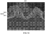
- Fig. 10 is a diagram for description of a method of calculating the surface area of the coating 450.
- the dendrite structure 450A included in the irregular structure of the coating 450 is dendritically formed.
- the dendrite structure 450A is divided into a primary structure 451 formed on the copper surface 11, and a secondary structure 452 formed as a branch from the primary structure 451, and the surface area of the coating 13 is considered.
- the average height of the primary structure 451 is 0.25 ⁇ m, and the average diameter of the primary structure 451 is 0.06 ⁇ m.
- 15 primary structures 451 are formed per 1 ⁇ m on the copper surface 11
- a large number of primary structures 451 are mainly formed at, among a protruding part 121 and a recessed part 120 included in the periodic structure 12, the protruding part 121 as illustrated in Fig. 10 . Accordingly, when the protruding part 121 and the recessed part 120 have an area ratio of 3:1, the number of primary structures 451 formed at the protruding part 121 is 168.
- the number of primary structures 451 formed per 1 ⁇ m 2 on the copper surface 11 is set to be 160.
- the average height of the secondary structure 452 is 0.012 ⁇ m, and the average diameter of the secondary structure 452 is 0.025 ⁇ m so that 50 secondary structures 452 are formed for each primary structure 451.
- the surface area of the primary structure 451 can be estimated to be 7.992 ⁇ m 2 for each 1 ⁇ m 2 of the surface area of the copper surface 11 with the upper and side areas of the primary structure 451 taken into account.
- the surface area of the secondary structure 452 can be estimated to be 7.540 ⁇ m 2 for each 1 ⁇ m 2 of the surface area of the copper surface 11 with the side area of the secondary structure 452 taken into account.
- the surface area of the copper surface 11 increases to 1.2 ⁇ m 2 for each 1 ⁇ m 2 .
- the surface area of the surface of the coating 13 on which the dendrite structure 450A as an irregular structure is formed is set to be at least 10 times larger than the surface area of the copper surface 11, the area of adhesion with the resin material 20 can be reliably increased as compared to a case in which the resin material 20 is directly adhered to the copper surface 11, thereby reliably improving adhesion between the copper foil 10 and the resin material 20.
- a first peeling test two kinds of composite materials each produced by bonding the M surface of the copper foil to a resin substrate made of FR4 R-1766, which is manufactured by Panasonic Corporation, with or without laser processing were prepared.
- the copper foil was joined to R-1766, which is manufactured by Panasonic Corporation, at a curing temperature of 170°C for a curing time of one hour.
- the tensile strength (peel strength) when these prepared composite materials were each cut and peeled off was measured.
- the resin side of each produced measurement sample was fixed by a support clasp, and the copper foil was peeled off in the direction at 90° to the measurement sample at the speed of 50 mm/minute to measure the peeling strength.
- the peel width was 10 mm ⁇ 0.1 mm.
- the peeling strength was measured by using TENSILON UMT-4-100 manufactured by Toyo Baldwin Ltd.
- a bar graph on the left side represents the tensile strength of the composite material (comparative example) obtained by bonding copper foil not provided with laser processing to a resin material
- a bar graph on the right side represents the tensile strength of the composite material (example) obtained by bonding copper foil provided with laser processing to a resin material.
- the tensile strength was improved by 16% approximately by performing laser processing on the copper foil.
- the tensile strength (peel strength) when these prepared composite materials were each cut and peeled off was measured.
- the resin side of each produced measurement sample was fixed by a support clasp, and the copper foil was peeled off in the direction at 90° to the measurement sample at the speed of 50 mm/minute to measure the peeling strength.
- the peel width was 10 mm ⁇ 0.1 mm.
- the peeling strength was measured by using TENSILON UMT-4-100 manufactured by Toyo Baldwin Ltd.
- a bar graph on the left side represents the tensile strength of the composite material (comparative example) obtained by bonding copper foil not provided with laser processing to a resin material
- a bar graph on the right side represents the tensile strength of the composite material (example) obtained by bonding copper foil provided with laser processing to a resin material.
- the tensile strength was improved by 86% approximately by performing laser processing on the copper foil.
- the tensile strength (peel strength) when these prepared composite materials were each cut and peeled off was measured.
- the resin side of each produced measurement sample was fixed by a support clasp, and the copper foil was peeled off in the direction at 90° to the measurement sample at the speed of 50 mm/minute to measure the peeling strength.
- the peel width was 10 mm ⁇ 0.1 mm.
- the peeling strength was measured by using TENSILON UMT-4-100 manufactured by Toyo Baldwin Ltd.
- a bar graph on the left side represents the tensile strength of the composite material (comparative example) obtained by bonding copper foil not provided with laser processing to a resin material
- a bar graph on the right side represents the tensile strength of the composite material (example) obtained by bonding copper foil provided with laser processing to a resin material.
- the tensile strength was improved by 128% approximately by performing laser processing on the copper foil.
- the periodic structure and the coating function as an anchor when joined with a resin material, thereby improving adhesion with the resin material.
- a periodic structure on the order of the laser wavelength is formed on the copper surface 11 of the copper foil 10
- a high-frequency signal can be transmitted at low loss
- the periodic structure functions as an anchor when joined with another member to have favorable adhesion with the member.
- the laser processing method according to the present embodiment is not limited the example described above but is applicable to, for example, a method of manufacturing a multi-layer printed circuit board as described below. Specifically, in the process of stacking press of a multi-layer printed circuit board, the upper surface of an inner-layer wire formed by etching is adhered to resin stacked above. Thus, the upper surface of the wire is required to be roughed.
- the laser processing according to the present embodiment described above has high position selectivity, and thus is preferable for roughing of the upper surface of a wire in such a multi-layer board manufacturing process.
- the processing beam diameter can be reduced up to 10 ⁇ m, and thus a fine wire having a width of 10 ⁇ m can be selectively roughed.
- the direction of a periodic structure can be changed in accordance with a wire by controlling polarization.
- a periodic structure having a period of 0.35 ⁇ m to 2 ⁇ m in a planar direction and a height of less than 1.5 ⁇ m can be formed parallel to a current conduction direction by controlling polarization.
- a fine periodic structure can be formed parallel to the direction of current flow by changing the direction of the periodic structure in this manner. Then, when such a fine periodic structure is formed parallel to the direction of current flow, it is possible to increase adhesion to resin while reducing degradation of a transmission loss as compared to a case in which the fine periodic structure is formed, for example, orthogonal to the direction of current flow.
- a dendrite structure is exemplarily described as an irregular structure formed on the coating 13, but the irregular structure may be another structure other than a dendrite structure as long as the surface area of the coating 13 is larger than the surface area of the copper surface 11.
Landscapes
- Engineering & Computer Science (AREA)
- Optics & Photonics (AREA)
- Physics & Mathematics (AREA)
- Chemical & Material Sciences (AREA)
- Mechanical Engineering (AREA)
- Microelectronics & Electronic Packaging (AREA)
- Manufacturing & Machinery (AREA)
- Plasma & Fusion (AREA)
- Organic Chemistry (AREA)
- Metallurgy (AREA)
- Materials Engineering (AREA)
- Chemical Kinetics & Catalysis (AREA)
- Laser Beam Processing (AREA)
- ing And Chemical Polishing (AREA)
- Manufacturing Of Printed Wiring (AREA)
- Lining Or Joining Of Plastics Or The Like (AREA)
Abstract
Description
- The present invention relates to a laser processing method of processing a copper surface by using laser, a joint method of joining copper foil to a resin material, and a copper member provided with surface processing.
- In the progress of diversification and high functionalities of materials along with rapid development of industries such as electronics and automobile, demand for members obtained by efficiently combining dissimilar materials of resin and metal, in particular, has been increasing for reduction of component weight, improvement of designing freedom, cost reduction, and the like.
- Typically, it is difficult to improve adhesion at a joint of a member obtained by combining dissimilar materials. For example, in a semiconductor package structure in which a substrate is molded by resin, particularly at high temperature, problems such as resin crack and chip flake occur due to insufficient adhesion between resin and metal, difference in thermal expansion rate between resin and a lead frame (metal), and expansion of water in the package.
- To solve the problems as described above, Patent Literatures 1 to 3 disclose technologies of roughing the surface of a metal member to form irregularity at a joint with a dissimilar material, in particular, thereby increasing adhesion at the joint.
-
- Patent Literature 1: Japanese Patent Application Laid-Open No.
1998-294024 - Patent Literature 2: Japanese Patent Application Laid-Open No.
2010-167475 - Patent Literature 3: Japanese Patent Application Laid-Open No.
2013-111881 - As described above, in the inventions according to Patent Literatures 1 to 3, the surface of a metal member is roughed to form irregularity at a joint with a dissimilar material. When a high-frequency signal is transmitted through copper foil, finer irregularity is desired to be formed on the copper surface to increase adhesion with a resin material while reducing a transmission loss due to the skin effect.
- However, it is difficult to apply the inventions according to Patent Literatures 1 to 3 to form fine irregularity on the surface of metal such as copper having significantly high thermal conductivity and low light absorptivity. Specifically, it needs to use ultrashort pulse laser of picoseconds or femtoseconds to form fine irregularity on the surface, but such ultrashort pulse laser has low processing efficiency due to the short duration of mutual interaction between light and metal, and laser itself is also expensive.
- In view of the the above-described problem, an object of the present invention is to provide a laser processing method capable of processing a copper surface to have a favorable electric characteristic and desirable adhesion with a resin material, a joint method of joining copper foil to a resin material, a copper member provided with surface processing, a method of manufacturing a multi-layer printed circuit board, and a multi-layer printed circuit board.
- A laser processing method according to one aspect of the present invention is a laser processing method of performing surface processing on a copper surface by using laser. The method is characterized by forming a periodic structure on the order of laser wavelength on the copper surface by irradiating the copper surface with pulse laser having a laser power close to a threshold beyond which copper processing is possible and having a pulse width on the order of nanoseconds. Specifically, the method manages the pulse width on the order of nanoseconds in a high fluence region, which has not been conventionally discussed, and forms a periodic structure on the order of laser wavelength on the copper surface. The fluence is a value obtained by dividing the peak power of the pulse laser by the beam area.
- With the above-described configuration, a periodic structure on the order of laser wavelength can be formed on a copper surface by irradiating the copper surface with pulse laser having a laser power close to a threshold beyond which copper processing is possible and having a pulse width on the order of nanoseconds. With such a periodic structure on the order of laser wavelength, a high-frequency signal can be transmitted at low loss, and the periodic structure functions as an anchor when joined with another member to have favorable adhesion with the member. In addition, when laser on the order of nanoseconds is used, fast and inexpensively processing can be achieved as compared to, for example, a case of using ultrashort pulse laser of picoseconds or femtoseconds.
- The laser processing method according to a preferable aspect of the present invention is characterized by forming a coating on the copper surface together with forming the periodic structure on the order of laser wavelength on the copper surface.
- The laser processing method according to a preferable aspect of the present invention is characterized by forming a dendrite structure having a period shorter than a period of the periodic structure on the order of laser wavelength by accumulating or depositing copper at a protruding part of the periodic structure on the order of laser wavelength.
- The laser processing method according to a preferable aspect of the present invention is characterized in that the copper surface is irradiated with pulse laser having a wavelength of 1000 nm to 1600 nm, a pulse width of 0.8 ns to 5.0 ns, and a fluence of 1.0×10⁸ W/cm2 to 4.0×10⁹ W/cm2 under air or atmosphere of oxygen, water, or active gas.
- The laser processing method according to a preferable aspect of the present invention is characterized in that the periodic structure is formed in a predetermined direction on the copper surface by irradiating the copper surface with the pulse laser while controlling the polarization direction of the pulse laser. According to the present aspect, anisotropic adhesion control to obtain strong adhesion in the predetermined direction and weak adhesion in a direction orthogonal to the predetermined direction can be achieved.
- The laser processing method according to a preferable aspect of the present invention is characterized in that the copper surface is irradiated with the pulse laser having an energy profile set in a top hat shape.
- The laser processing method according to a preferable aspect of the present invention is characterized in that an identical irradiation position on the copper surface is irradiated with the pulse laser while the fluence of the pulse laser is gradually reduced.
- A joint method according to one aspect of the present invention is a joint method of joining copper foil to a resin material. The method is characterized by forming a roughed part having a periodic structure on the order of laser wavelength on a surface of the copper foil by irradiating the surface of the copper foil with pulse laser having a laser power close to a threshold beyond which copper processing is possible and having a pulse width on the order of nanoseconds, and performs laser welding or heat press bonding of the roughed part formed on the surface of the copper foil to the resin material.
- In a copper member according to one aspect of the present invention, a periodic structure having a period of 0.35 µm to 2 µm in a planar direction and a height of less than 1.5 µm is formed on at least one surface.
- The copper member according to a preferable aspect of the present invention is characterized in that the ratio of the height of the periodic structure relative to the thickness of the copper member is 0.15% to 30% inclusive.
- The copper member according to a preferable aspect of the present invention is characterized in that a coating is formed on the periodic structure, and an irregular structure having a period shorter than a period of the periodic structure is formed on a surface of the coating.
- The copper member according to a preferable aspect of the present invention is characterized in that the surface area of the coating on which the irregular structure is formed is at least ten times larger than the surface area of the surface on which the periodic structure is formed.
- The copper member according to a preferable aspect of the present invention is characterized in that the irregular structure is made of a dendrite structure.
- The copper member according to a preferable aspect of the present invention is characterized in that the copper member is copper foil.
- A method of manufacturing a printed circuit board according to one aspect of the present invention is a printed circuit board manufacturing method of manufacturing a multi-layer printed circuit board. The method is characterized by forming a periodic structure on the order of laser wavelength at the inner-layer wiring part by selectively irradiating an inner-layer wiring part of the multi-layer printed circuit board with pulse laser having a laser power close to a threshold beyond which copper processing is possible and having a pulse width on the order of nanoseconds.
- The method of manufacturing a printed circuit board according to a preferable aspect of the present invention provides a multi-layer printed circuit board on which an inner-layer wiring part is formed, characterized in that a periodic structure having a period of 0.35 µm to 2 µm in a planar direction and a height of less than 1.5 µm is formed in parallel to a current conduction direction at the inner-layer wiring part.
- The present invention can provide a laser processing method capable of processing a copper surface to have a favorable electric characteristic and desirable adhesion with a resin material, a joint method of joining copper foil to a resin material, a copper member provided with surface processing, a method of manufacturing a multi-layer printed circuit board, and a multi-layer printed circuit board.
-
- [
Fig. 1 ] A diagram schematically illustrating a laser processing process of performing surface processing on a copper surface by using laser. - [
Fig. 2 ] A diagram illustrating evaluation of surface processing in which laser processing is performed under a plurality of kinds of conditions into four items of "processing", "mixed processing and coating removal", "coating removal", and "blackening" where the horizontal axis represents the pulse width [ns] and the vertical axis represents the fluence [W/cm2]. - [
Fig. 3 ] A diagram illustrating an image of acopper surface 11 provided with surface processing through the laser processing process, which is obtained through magnification of 2000 times by an electron microscope. - [
Fig. 4] Fig. 4(A) is an image of a sectional structure ofcopper foil 10 provided with surface processing by using pulse laser, which is obtained through magnification of 10000 times by an electron microscope; andFig. 4(B) is an image of a sectional structure of thecopper foil 10 provided with surface processing by using pulse laser, which is obtained through magnification of 50000 times by an electron microscope. - [
Fig. 5 ] A diagram illustrating a result of analysis of thecopper surface 11 of thecopper foil 10 after laser processing by X-ray photoelectron spectroscopy. - [
Fig. 6] Fig. 6(A) is a diagram illustrating a sectional structure of acomposite material 61 as a comparative example obtained by performing laser welding or heat press bonding of asurface 611 ofcopper foil 610 not provided with laser processing to aresin material 620; andFig. 6(B) is a diagram illustrating a sectional structure of acomposite material 100 obtained by performing laser welding or heat press bonding of thecopper surface 11 of thecopper foil 10 provided with laser processing to aresin material 20. - [
Fig. 7 ] A diagram for description of the method of performing a peeling test. - [
Fig. 8] Fig. 8(A) is a diagram illustrating peel strength obtained by preparing two kinds of composite materials each produced by bonding the M surface of copper foil to a resin substrate made of FR4 with or without laser processing, and performing the peeling test on each composite material;Fig. 8(B) is a diagram illustrating peel strength obtained by preparing two kinds of composite materials each produced by bonding the S surface of copper foil to a resin substrate made of FR4 with or without laser processing, and performing the peeling test on each composite material; andFig. 8(C) is a diagram illustrating peel strength obtained by preparing two kinds of composite materials each produced by bonding the S surface of copper foil to a resin substrate made of Megtron6 with or without laser processing, and performing the peeling test on each composite material. - [
Fig. 9 ] A diagram schematically illustrating thecopper foil 10 on which aperiodic structure 12 is formed by the laser processing process according to the present embodiment. - [
Fig. 10 ] A diagram for description of the method of calculating the surface area of acoating 450. - The following describes an embodiment for achieving the present invention (hereinafter referred to as the present embodiment) with specific examples. The present embodiment relates to a laser processing method of performing surface processing on a copper surface by using laser.
-
Fig. 1 is a diagram schematically illustrating a laser processing process of performing surface processing on a copper surface by using laser. In the laser processing process according to the present embodiment, acopper surface 11 of acopper member 10 is irradiated with pulse laser having a pulse width managed on the order of nanoseconds in a high fluence region, which has not been conventionally discussed. Specifically, as illustrated inFig. 1 , thecopper surface 11 of thecopper member 10 is irradiated withpulse laser 2 having a laser power close to a threshold beyond which copper processing is possible and having a pulse width on the order of nanoseconds. The order of nanoseconds indicates, for example, the range of 0.8 ns to 5.0 ns. The fluence is a value obtained by dividing the peak power of the pulse laser by the beam area. - The
copper member 10 is made of a metallic material containing copper (Cu) as a primary component, and is, for example, a copper plate. In the present embodiment, such a copper plate having a thickness of 500 µm or lessis referred to as copper foil. In the present embodiment, as an example, thecopper member 10 is copper foil, and referred to as "copper foil 10" below. - The following describes characteristics of a copper foil surface processed by laser having different values of the fluence [W/cm2] and the pulse width [ns] as laser power.
Fig. 2 is a diagram illustrating evaluation of surface processing in which laser processing is performed under a plurality of kinds of conditions into four items of "processing", "mixed processing and coating removal", "coating removal", and "blackening" where the horizontal axis represents the pulse width [ns] and the vertical axis represents fluence [W/cm2]. - The "processing" refers to a processing in which copper is removed through melting and evaporation due to ablation or heat input to form a groove in a size equivalent to the diameter of a processing beam, the "coating removal" refers to processing in which only a copper compound coating such as rust on the copper foil surface is removed, the "mixed processing and coating removal" refers to processing in which the processing and the coating removal are simultaneously performed, and the "blackening" refers to processing in a middle region between the "processing" and the "coating removal", in which a coating of oxide or the like on the copper foil surface and a fine periodic structure on the order of laser wavelength are simultaneously formed. The beam diameter refers to the spot size of a Gaussian beam. When the processing is performed with the Gaussian beam, a copper surface layer is removed at a central part of the beam, at which the fluence is high, in the blackening in some cases. Thus, it is more preferable that the processing beam has an energy profile in a top hat shape than a Gaussian shape. Accordingly, it is preferable to set the energy profile of the pulse laser in a top hat shape.
- The evaluation illustrated in
Fig. 2 indicates it is preferable to perform processing at a fluence and a pulse width between the "processing" and the "coating removal". Specifically, a laser processing condition of a pulse width (first pulse width) and a fluence (first fluence) with which formation of a groove in a size equivalent to the processing beam diameter on thecopper surface 11 is possible, and a laser processing condition of a pulse width (second pulse) and a fluence (second fluence) that have values smaller than the values of the first pulse width and the first fluence, respectively and with which removal of only a copper compound coating from thecopper surface 11 is possible are acquired and stored as profile data in advance in, for example, a storage provided to a laser processing apparatus. Then, the laser processing apparatus forms a periodic structure on the order of laser wavelength by referring to the profile data and irradiating thecopper surface 11 with pulse laser having a pulse width set to be between the first pulse width and the second pulse width and a fluence set to be between the first fluence and the second fluence. When pulse laser set to have a pulse width of 0.8 ns to 5.0 ns and a fluence of 1.0×10⁸ W/cm2 to 4.0×10⁹ W/cm2, which are specific numerical values obtained from the result illustrated inFig. 2 , is used, pulse energy is close to a processing threshold of the copper foil, and aperiodic structure 12 and acoating 13 can be formed on thecopper surface 11 of thecopper foil 10 as illustrated inFig. 1 . - In particular, it is preferable that such pulse laser having a laser power close to a threshold beyond which copper processing is possible and having a pulse width on the order of nanoseconds satisfy conditions as follows.
- The pulse width on the order of nanoseconds has a range of 0.8 ns to 999 ns.
- Specifically, it is preferable to irradiate the
copper surface 11 with pulse laser having a wavelength of 1000 nm to 1600 nm, a pulse width of 0.8 ns to 999 ns, and a fluence of 1.0×10⁸ W/cm2 to 4.0×10⁹ W/cm2 in air under atmosphere of oxygen, water, or active gas. - It is more preferable that the
copper surface 11 be irradiated with pulse laser having a wavelength of 1000 nm to 1600 nm, a pulse width of 0.8 ns to 5.0 ns, and a fluence of 1.0×10⁸ W/cm2 to 4.0×10⁹ W/cm2 under air or atmosphere of oxygen, water, or active gas. - It is still more preferable that the
copper surface 11 be irradiated with pulse laser having a wavelength of 1000 nm to 1600 nm, a pulse width of 1.0 ns to 5.0 ns, and a fluence of 1.0×10⁸ W/cm2 to 4.0×10⁹ W/cm2 under air or atmosphere of oxygen, water, or active gas. - Copper causes improvement of light absorptivity and decrease of thermal conductivity when an oxide coating is formed on the surface thereof, and laser processing is promoted accordingly. Thus, it is preferable that, when an identical place is processed by laser several times, the processing be performed while the fluence is gradually reduced.
- The periodic structure is formed orthogonal to the polarization direction of a processing beam. Thus, a structure having periodicity in an optional direction (predetermined direction) can be formed by irradiating the
copper surface 11 with pulse laser while controlling the polarization direction of the pulse laser through a wave plate or the like. Anisotropic adhesion control to obtain strong adhesion in the predetermined direction and weak adhesion in a direction orthogonal to the predetermined direction can be achieved by forming the periodic structure in the predetermined direction in this manner. - The
periodic structure 12 and thecoating 13 on the order of wavelength can be formed on thecopper surface 11 of thecopper foil 10 by appropriately controlling the fluence so that the laser power becomes close to the threshold beyond which copper processing is possible as described above. The order of wavelength has, for example, a range of 1000 nm to 1600 nm. A periodic structure of 1000 nm or less may be formed by shortening the laser wavelength. - In particular, it is preferable to repeatedly irradiate the
copper surface 11 with pulse laser having at least one of parameters of frequency, laser intensity, scanning speed, spot size, wavelength, and atmosphere adjusted in accordance with the height and shape of theperiodic structure 12 to be formed on thecopper surface 11. - As described above, the laser processing process according to the present embodiment forms the
periodic structure 12 on the order of the laser wavelength by irradiating thecopper surface 11 with pulse laser having a pulse width managed on the order of nanoseconds in a high fluence region, which has not been conventionally discussed. Specifically, theperiodic structure 12 on the order of the laser wavelength can be formed on thecopper surface 11 by irradiating thecopper surface 11 with pulse laser having a laser power close to the threshold beyond which copper processing is possible and having a pulse width on the order of nanoseconds. In addition, when laser on the order of nanoseconds is used, fast and inexpensively processing can be achieved as compared to, for example, a case of using ultrashort pulse laser of picoseconds or femtoseconds. -
Fig. 9 is a diagram schematically illustrating thecopper foil 10 on which theperiodic structure 12 is formed through the laser processing process according to the present embodiment. - As illustrated in
Fig. 9 , when L1 represents the thickness of thecopper foil 10, in other words, the distance between thecopper surface 11 and a back surface 14 facing to thecopper surface 11, and L2 represents the height of theperiodic structure 12, in other words, the distance between thecopper surface 11 and the bottom surface of a recessed part (groove) 120 forming theperiodic structure 12, the ratio of the height L2 of theperiodic structure 12 relative to the thickness L1 of thecopper foil 10 is 0.15% to 30% inclusive. - The following describes the
periodic structure 12 and thecoating 13 in detail. -
Fig. 3 illustrates an image of thecopper surface 11 provided with surface processing through the above-described laser processing process, which is obtained through magnification of 2000 times by an electron microscope. As understood fromFig. 3 , an uniformperiodic structure 200 of 1200 nm approximately is formed on the surface of the copper foil. -
Fig. 4 is an image illustrating a sectional structure of thecopper foil 10 provided with surface processing by using pulse laser. Specifically,Fig. 4(A) is an image obtained through magnification at 10000 times by an electron microscope, andFig. 4(B) is an image obtained through magnification at 50000 times by an electron microscope. As understood fromFig. 4(A) , aperiodic structure 400 having a height of 400 nm approximately is formed in about eight periods per 10000 nm (10 µm), in other words, in the period of 1250 nm. As illustrated inFig. 4(B) in an enlarged view of theperiodic structure 400, acoating 450 in a dendrite structure as an irregular structure having a shorter period and a height of 400 nm approximately is formed on theperiodic structure 400. -
Fig. 5 illustrates a result of analysis of thecopper surface 11 of thecopper foil 10 after the laser processing by X-ray photoelectron spectroscopy. Specifically,Fig. 5 illustrates a result of analysis of the copper foil after the laser processing with a solid line, and illustrates, as a comparative example, a result of analysis of the copper foil before the laser processing with a dashed line. InFig. 5 , binding energy E1 corresponds to a measured value of organic C-O bond, binding energy E2 corresponds to a measured value of organic C=O bond of Cu hydroxide, binding energy E3 corresponds to a measured value of Cu2O, and binding energy E4 corresponds to a measured value of CuO. Increase of Cu hydroxide and CuO in the copper foil after the laser processing as compared to the unprocessed copper foil is observed in a result of comparison between the solid line and the dashed line inFig. 5 , which clearly indicates that an oxide coating is formed on the copper surface. - For example, when the copper foil is used for usage on a printed circuit board or the like and it is not preferable that the
oxide coating 450 remain, theoxide coating 450 can be removed through cleaning with dilute sulfuric acid. In such a case, too, theperiodic structure 400 may remain. - As understood from
Fig. 3 to Fig. 5 described above, the periodic structure 12 (1200 nm approximately) and thecoating 13 on the order of wavelength are formed on thecopper surface 11 of thecopper foil 10. With theperiodic structure 12 and thecoating 13, a high-frequency signal can be transmitted at low loss, and theperiodic structure 12 and thecoating 13 function as an anchor when joined with another member to have favorable adhesion with the member for the following reason. -
Fig. 6(A) is a diagram illustrating a sectional structure of acomposite material 61 obtained by performing laser welding or heat press bonding of asurface 611 ofcopper foil 610 not provided with laser processing to aresin material 620 as a comparative example. Thesurface 611 of thecopper foil 610 according to the comparative example as illustrated inFig. 6(A) has a shape more irregular in the height (thickness) direction than that of thecopper surface 11 of thecopper foil 10 according to the present embodiment described above due to, for example, a manufacturing process. Thus, when a high-frequency signal is caused to flow through thecopper foil 610, the signal flows up and down along the irregularity of thesurface 611 due to the skin effect, which leads to an increased resistance. -
Fig. 6(B) is a diagram illustrating a sectional structure of acomposite material 100 obtained by performing laser welding or heat press bonding of thecopper surface 11 of thecopper foil 10 provided with laser processing to aresin material 20. As illustrated in the cross-sectional view inFig. 6(B) , the irregularity of thecopper surface 11 of thecopper foil 10 in the height (thickness) direction is smaller than that of thesurface 611 of thecopper foil 610 according to the comparative example due to the periodic structure and the coating described above. Thus, when a high-frequency signal is caused to flow through thecopper foil 10, the signal flows up and down along the irregularity of thecopper surface 11 due to the skin effect, but the height of the irregularity is smaller than that of thesurface 611 described above, which leads to a decreased resistance. - In addition, the periodic structure formed on the
copper surface 11 exerts an anchor effect, thereby improving adhesion to theresin material 20. The oxide coating formed on thecopper surface 11 promotes formation of chemical bond to theresin material 20, and contributes improvement of chemical adhesion between thecopper foil 10 and theresin material 20. - In particular, the
copper foil 10 is preferable because a periodic structure having a period of 0.35 µm to 2 µm in a planar direction and a height of less than 1.5 µm is formed on thecopper surface 11 so that the resistance can be reduced particularly when a high-frequency signal of 1 GHz band or higher is transmitted. As a specific reason, when the frequency of an electric signal is 1 GHz or higher, the influence of the skin effect that current flows only through the surface of a conductor is significant so that the influence of increase of a conductor loss caused by change of a current transmission path due to the irregularity of the surface cannot be ignored. - It is possible to reliably improve adhesion between the
copper foil 10 and theresin material 20 by setting the surface area of the surface of thecoating 13, on which an irregular structure is formed, to be at least 10 times larger than the surface area of thecopper surface 11, on which theperiodic structure 12 is formed. - The following describes numerical examples of the surface area of the
copper surface 11 on which theperiodic structure 12 is formed and the surface area of the coating 13 (coating 450) on which adendrite structure 450A is formed. -
Fig. 10 is a diagram for description of a method of calculating the surface area of thecoating 450. - As illustrated in
Fig. 10 , thedendrite structure 450A included in the irregular structure of thecoating 450 is dendritically formed. Thus, thedendrite structure 450A is divided into aprimary structure 451 formed on thecopper surface 11, and asecondary structure 452 formed as a branch from theprimary structure 451, and the surface area of thecoating 13 is considered. - Assume that the average height of the
primary structure 451 is 0.25 µm, and the average diameter of theprimary structure 451 is 0.06 µm. When 15primary structures 451 are formed per 1µm on thecopper surface 11, 225 (= 15x15)primary structures 451 are formed per 1µm2 on thecopper surface 11. A large number ofprimary structures 451 are mainly formed at, among a protruding part 121 and a recessedpart 120 included in theperiodic structure 12, the protruding part 121 as illustrated inFig. 10 . Accordingly, when the protruding part 121 and the recessedpart 120 have an area ratio of 3:1, the number ofprimary structures 451 formed at the protruding part 121 is 168. Thus, the number ofprimary structures 451 formed per 1µm2 on thecopper surface 11 is set to be 160. - Assume that the average height of the
secondary structure 452 is 0.012 µm, and the average diameter of thesecondary structure 452 is 0.025 µm so that 50secondary structures 452 are formed for eachprimary structure 451. - In this case, the surface area of the
primary structure 451 can be estimated to be 7.992 µm2 for each 1 µm2 of the surface area of thecopper surface 11 with the upper and side areas of theprimary structure 451 taken into account. The surface area of thesecondary structure 452 can be estimated to be 7.540 µm2 for each 1 µm2 of the surface area of thecopper surface 11 with the side area of thesecondary structure 452 taken into account. Thus, the surface area of thecoating 450 on which thedendrite structure 450A is formed can be estimated to be 15.53 (= 7.992 + 7.540) µm2. - When the area improvement rate of the
copper surface 11 due to formation of theperiodic structure 12 is 20%, the surface area of thecopper surface 11 increases to 1.2 µm2 for each 1 µm2. - Accordingly, in the case illustrated in
Fig. 10 , the surface area of the surface of thecoating 450 is about 12.94 (= 15.53/1.2) times larger than the surface area of thecopper surface 11. - In this manner, when the surface area of the surface of the
coating 13 on which thedendrite structure 450A as an irregular structure is formed is set to be at least 10 times larger than the surface area of thecopper surface 11, the area of adhesion with theresin material 20 can be reliably increased as compared to a case in which theresin material 20 is directly adhered to thecopper surface 11, thereby reliably improving adhesion between thecopper foil 10 and theresin material 20. - Subsequently, as a peeling test to evaluate adhesion performance of copper foil having a surface provided with laser processing and copper foil having a surface not provided with laser processing, force (tensile strength) necessary for peeling off the
copper foil 71 in the direction of arrow Y was measured for ajoint material 70 obtained by joiningcopper foil 71 to aresin material 72 as illustrated inFig. 7 . - Specifically, in a first peeling test, two kinds of composite materials each produced by bonding the M surface of the copper foil to a resin substrate made of FR4 R-1766, which is manufactured by Panasonic Corporation, with or without laser processing were prepared. The copper foil was joined to R-1766, which is manufactured by Panasonic Corporation, at a curing temperature of 170°C for a curing time of one hour.
- Then, the tensile strength (peel strength) when these prepared composite materials were each cut and peeled off was measured. Specifically, the resin side of each produced measurement sample was fixed by a support clasp, and the copper foil was peeled off in the direction at 90° to the measurement sample at the speed of 50 mm/minute to measure the peeling strength. The peel width was 10 mm ± 0.1 mm. The peeling strength was measured by using TENSILON UMT-4-100 manufactured by Toyo Baldwin Ltd.
- In
Fig. 8(A) , a bar graph on the left side represents the tensile strength of the composite material (comparative example) obtained by bonding copper foil not provided with laser processing to a resin material, and a bar graph on the right side represents the tensile strength of the composite material (example) obtained by bonding copper foil provided with laser processing to a resin material. As understood fromFig. 8(A) , the tensile strength was improved by 16% approximately by performing laser processing on the copper foil. - In a second peeling experiment, two kinds of composite materials each produced by bonding the S surface of copper foil to a resin substrate made of FR4 R-1766, which is manufactured by Panasonic Corporation, with or without laser processing were prepared. The copper foil was joined to R-1766, which is manufactured by Panasonic Corporation, at a curing temperature of 170°C for a curing time of one hour.
- Then, the tensile strength (peel strength) when these prepared composite materials were each cut and peeled off was measured. Specifically, the resin side of each produced measurement sample was fixed by a support clasp, and the copper foil was peeled off in the direction at 90° to the measurement sample at the speed of 50 mm/minute to measure the peeling strength. The peel width was 10 mm ± 0.1 mm. The peeling strength was measured by using TENSILON UMT-4-100 manufactured by Toyo Baldwin Ltd.
- In
Fig. 8(B) , a bar graph on the left side represents the tensile strength of the composite material (comparative example) obtained by bonding copper foil not provided with laser processing to a resin material, and a bar graph on the right side represents the tensile strength of the composite material (example) obtained by bonding copper foil provided with laser processing to a resin material. As understood fromFig. 8(B) , the tensile strength was improved by 86% approximately by performing laser processing on the copper foil. - In a third peeling experiment, two kinds of composite materials each produced by bonding the S surface of copper foil to a resin substrate made of MEGTRON6 R-5670 with or without laser processing were prepared. The copper foil was joined to MEGTRON6 R-5670 at a curing temperature of 200°C for a curing time of two hours.
- Then, the tensile strength (peel strength) when these prepared composite materials were each cut and peeled off was measured. Specifically, the resin side of each produced measurement sample was fixed by a support clasp, and the copper foil was peeled off in the direction at 90° to the measurement sample at the speed of 50 mm/minute to measure the peeling strength. The peel width was 10 mm ± 0.1 mm. The peeling strength was measured by using TENSILON UMT-4-100 manufactured by Toyo Baldwin Ltd.
- In
Fig. 8(C) , a bar graph on the left side represents the tensile strength of the composite material (comparative example) obtained by bonding copper foil not provided with laser processing to a resin material, and a bar graph on the right side represents the tensile strength of the composite material (example) obtained by bonding copper foil provided with laser processing to a resin material. As understood fromFig. 8(C) , the tensile strength was improved by 128% approximately by performing laser processing on the copper foil. - As understood from the measurement results of the tensile strength illustrated in
Fig. 8 described above, when laser processing is performed on copper foil to form a periodic structure and a coating, the periodic structure and the coating function as an anchor when joined with a resin material, thereby improving adhesion with the resin material. - As described above with reference to
Figs. 6 to 8 , when a periodic structure on the order of the laser wavelength is formed on thecopper surface 11 of thecopper foil 10, a high-frequency signal can be transmitted at low loss, and the periodic structure functions as an anchor when joined with another member to have favorable adhesion with the member. - The laser processing method according to the present embodiment is not limited the example described above but is applicable to, for example, a method of manufacturing a multi-layer printed circuit board as described below. Specifically, in the process of stacking press of a multi-layer printed circuit board, the upper surface of an inner-layer wire formed by etching is adhered to resin stacked above. Thus, the upper surface of the wire is required to be roughed. The laser processing according to the present embodiment described above has high position selectivity, and thus is preferable for roughing of the upper surface of a wire in such a multi-layer board manufacturing process. For this reason, it is preferable to form a periodic structure on the order of the laser wavelength at an inner-layer wiring part of the multi-layer printed circuit board by selectively irradiating the inner-layer wiring part with pulse laser having a laser power close to a threshold beyond which copper processing is possible and having a pulse width on the order of nanoseconds. In particular, for example, the processing beam diameter can be reduced up to 10 µm, and thus a fine wire having a width of 10 µm can be selectively roughed.
- In addition, the direction of a periodic structure can be changed in accordance with a wire by controlling polarization. Specifically, a periodic structure having a period of 0.35 µm to 2 µm in a planar direction and a height of less than 1.5 µm can be formed parallel to a current conduction direction by controlling polarization. Thus, a fine periodic structure can be formed parallel to the direction of current flow by changing the direction of the periodic structure in this manner. Then, when such a fine periodic structure is formed parallel to the direction of current flow, it is possible to increase adhesion to resin while reducing degradation of a transmission loss as compared to a case in which the fine periodic structure is formed, for example, orthogonal to the direction of current flow.
- In the above-described embodiment, a dendrite structure is exemplarily described as an irregular structure formed on the
coating 13, but the irregular structure may be another structure other than a dendrite structure as long as the surface area of thecoating 13 is larger than the surface area of thecopper surface 11. -
- 10
- copper foil
- 11
- copper surface
- 12
- periodic structure
- 13
- coating
- 2
- pulse laser
- 450A
- dendrite structure
Claims (18)
- A laser processing method of performing surface processing on a copper surface by using laser,
the method being characterized by forming a periodic structure on an order of laser wavelength on the copper surface by irradiating the copper surface with pulse laser having a laser power close to a threshold beyond which copper processing is possible and having a pulse width on an order of nanoseconds. - The laser processing method according to claim 1, characterized by forming a coating on the copper surface together with forming the periodic structure on the order of laser wavelength on the copper surface.
- The laser processing method according to claim 1 or 2, characterized by forming a dendrite structure having a period shorter than a period of the periodic structure on the order of laser wavelength by accumulating or depositing copper at a protruding part of the periodic structure on the order of laser wavelength.
- The laser processing method according to any one of claims 1 to 3, characterized in that the periodic structure on the order of laser wavelength is formed by:referring to a laser processing condition of a first pulse width and a first fluence with which formation of a groove in a size equivalent to a processing beam diameter on the copper surface is possible, and a laser processing condition of a second pulse width and a second fluence that have values smaller than values of the first pulse width and the first fluence, respectively, and with which removal of only a copper compound coating from the copper surface is possible, andirradiating the copper surface with pulse laser having a pulse width set to be between the first pulse width and the second pulse width and a fluence set to be between the first fluence and the second fluence.
- The laser processing method according to any one of claims 1 to 4, characterized in that the copper surface is irradiated with pulse laser having a wavelength of 1000 nm to 1600 nm, a pulse width of 0.8 ns to 5.0 ns, and a fluence of 1.0×10⁸ W/cm2 to 4.0×10⁹ W/cm2 under air or atmosphere of oxygen, water, or active gas.
- The laser processing method according to any one of claims 1 to 5, characterized in that the copper surface is repeatedly irradiated with pulse laser having at least one of parameters of frequency, laser intensity, scanning speed, spot size, wavelength, and atmosphere adjusted in accordance with a height and shape of a periodic structure to be formed on the copper surface.
- The laser processing method according to any one of claims 1 to 6, characterized in that the periodic structure is formed in a predetermined direction on the copper surface by irradiating the copper surface with the pulse laser while controlling a polarization direction of the pulse laser.
- The laser processing method according to any one of claims 1 to 7, characterized in that the copper surface is irradiated with the pulse laser having an energy profile set in a top hat shape.
- The laser processing method according to any one of claims 1 to 8, characterized in that an identical irradiation position on the copper surface is irradiated with the pulse laser while the fluence of the pulse laser is gradually reduced.
- A joint method of joining copper foil to a resin material, the method being characterized by comprising:forming a roughed part having a periodic structure on an order of laser wavelength on a surface of the copper foil by irradiating the surface of the copper foil with pulse laser having a laser power close to a threshold beyond which copper processing is possible and having a pulse width on an order of nanoseconds; andperforming laser welding or heat press bonding of the roughed part formed on the surface of the copper foil to the resin material.
- A copper member characterized in that, on at least one surface of the copper member, a periodic structure having a period of 0.35 µm to 2 µm in a planar direction and a height of less than 1.5 µm is formed.
- The copper member according to claim 11, characterized in that the ratio of the height of the periodic structure relative to a thickness of the copper member is 0.15% to 30% inclusive.
- The copper member according to claim 11 or 12, characterized in that
a coating is formed on the periodic structure, and
an irregular structure having a period shorter than a period of the periodic structure is formed on a surface of the coating. - The copper member according to claim 13, characterized in that a surface area of the coating on which the irregular structure is formed is at least ten times larger than a surface area of the surface on which the periodic structure is formed.
- The copper member according to claim 13 or 14, characterized in that the irregular structure is made of a dendrite structure.
- The copper member according to claim 12 or 13, characterized in that the copper member is copper foil.
- A printed circuit board manufacturing method of manufacturing a multi-layer printed circuit board, the method being characterized by forming a periodic structure on an order of laser wavelength at an inner-layer wiring part of the multi-layer printed circuit board by selectively irradiating the inner-layer wiring part with pulse laser having a laser power close to a threshold beyond which copper processing is possible and having a pulse width on an order of nanoseconds.
- A multi-layer printed circuit board on which an inner-layer wiring part is formed, characterized in that a periodic structure having a period of 0.35 µm to 2 µm in a planar direction and a height of less than 1.5 µm is formed in parallel to a current conduction direction at the inner-layer wiring part.
Applications Claiming Priority (2)
| Application Number | Priority Date | Filing Date | Title |
|---|---|---|---|
| JP2016147575 | 2016-07-27 | ||
| PCT/JP2017/026996 WO2018021392A1 (en) | 2016-07-27 | 2017-07-26 | Laser treatment method, bonding method, copper member, method for manufacturing multilayer print wiring substrate, and multilayer print wiring substrate |
Publications (2)
| Publication Number | Publication Date |
|---|---|
| EP3492211A1 true EP3492211A1 (en) | 2019-06-05 |
| EP3492211A4 EP3492211A4 (en) | 2020-09-02 |
Family
ID=61017561
Family Applications (1)
| Application Number | Title | Priority Date | Filing Date |
|---|---|---|---|
| EP17834394.3A Withdrawn EP3492211A4 (en) | 2016-07-27 | 2017-07-26 | Laser treatment method, bonding method, copper member, method for manufacturing multilayer print wiring substrate, and multilayer print wiring substrate |
Country Status (5)
| Country | Link |
|---|---|
| US (1) | US20190166701A1 (en) |
| EP (1) | EP3492211A4 (en) |
| JP (1) | JP6887210B2 (en) |
| CN (1) | CN109496172A (en) |
| WO (1) | WO2018021392A1 (en) |
Cited By (1)
| Publication number | Priority date | Publication date | Assignee | Title |
|---|---|---|---|---|
| EP4245522A4 (en) * | 2022-01-27 | 2024-05-01 | Mutsuki Electric Co., Ltd. | METAL ELEMENT, METAL-RESIN BONDED BODY AND METHOD FOR MANUFACTURING A METAL-RESIN BONDED BODY |
Families Citing this family (6)
| Publication number | Priority date | Publication date | Assignee | Title |
|---|---|---|---|---|
| JP7188572B2 (en) * | 2019-05-10 | 2022-12-13 | 昭和電工マテリアルズ株式会社 | Joining metal member and joined body |
| WO2020230198A1 (en) * | 2019-05-10 | 2020-11-19 | 昭和電工マテリアルズ株式会社 | Joining metal member and joining body |
| CN110996557A (en) * | 2020-01-15 | 2020-04-10 | 深圳市聚永能科技有限公司 | Method and apparatus for laser roughening copper foil surface of printed circuit board |
| EP4219063A4 (en) * | 2020-09-25 | 2024-11-06 | Furukawa Electric Co., Ltd. | LASER TREATMENT METHOD AND DEVICE |
| CN112928280B (en) * | 2021-03-10 | 2022-06-07 | 中国科学院金属研究所 | Patterning method of copper foil for lithium metal negative electrode |
| CN119450951B (en) * | 2024-11-18 | 2026-07-17 | 陕西西部新材科技有限公司 | Laser reflectivity-based copper-chromium alloy copper foil, method, circuit board and device |
Family Cites Families (13)
| Publication number | Priority date | Publication date | Assignee | Title |
|---|---|---|---|---|
| JPH06212451A (en) * | 1993-01-11 | 1994-08-02 | Osaka Prefecture | Metal surface decoration processing method |
| US5473138A (en) * | 1993-07-13 | 1995-12-05 | Singh; Rajiv K. | Method for increasing the surface area of ceramics, metals and composites |
| WO2004035255A1 (en) * | 2002-09-27 | 2004-04-29 | Nec Machinery Corporation | Cyclic structure formation method and surface treatment method |
| JP4644797B2 (en) * | 2004-01-28 | 2011-03-02 | 国立大学法人京都大学 | Laser irradiation method and apparatus, fine processing method and apparatus, and thin film forming method and apparatus |
| JP4791745B2 (en) * | 2005-03-28 | 2011-10-12 | パナソニック電工株式会社 | Method of processing light incident / exit part of optical medium |
| JP5242710B2 (en) * | 2010-01-22 | 2013-07-24 | 古河電気工業株式会社 | Roughening copper foil, copper clad laminate and printed wiring board |
| JP2013242475A (en) * | 2012-05-22 | 2013-12-05 | Panasonic Corp | Optoelectric substrate, optical module and method of manufacturing optoelectric substrate |
| DE102012112550A1 (en) * | 2012-12-18 | 2014-06-18 | Lpkf Laser & Electronics Ag | Method for metallizing a workpiece and a layer structure of a workpiece and a metal layer |
| JP2015124426A (en) * | 2013-12-27 | 2015-07-06 | 株式会社Shカッパープロダクツ | Surface-treated copper foil and laminate |
| CN104439699B (en) * | 2014-10-27 | 2016-06-29 | 中国科学院理化技术研究所 | A system and method for laser preparation of micro-nano array structure |
| CN104439956B (en) * | 2014-11-18 | 2017-04-19 | 清华大学 | Method for connecting materials difficult to connect through ultrafast lasers |
| CN104439708B (en) * | 2014-11-18 | 2016-09-21 | 清华大学 | A kind of ultra-hydrophobic high sticking metal surface and preparation method thereof |
| CN104649233B (en) * | 2015-01-19 | 2017-01-11 | 清华大学 | Controllable patterning ultrafast laser composite preparation method for metal oxide nano wires |
-
2017
- 2017-07-26 EP EP17834394.3A patent/EP3492211A4/en not_active Withdrawn
- 2017-07-26 WO PCT/JP2017/026996 patent/WO2018021392A1/en not_active Ceased
- 2017-07-26 JP JP2018530344A patent/JP6887210B2/en active Active
- 2017-07-26 CN CN201780046832.9A patent/CN109496172A/en active Pending
-
2019
- 2019-01-25 US US16/258,447 patent/US20190166701A1/en not_active Abandoned
Cited By (1)
| Publication number | Priority date | Publication date | Assignee | Title |
|---|---|---|---|---|
| EP4245522A4 (en) * | 2022-01-27 | 2024-05-01 | Mutsuki Electric Co., Ltd. | METAL ELEMENT, METAL-RESIN BONDED BODY AND METHOD FOR MANUFACTURING A METAL-RESIN BONDED BODY |
Also Published As
| Publication number | Publication date |
|---|---|
| US20190166701A1 (en) | 2019-05-30 |
| WO2018021392A1 (en) | 2018-02-01 |
| EP3492211A4 (en) | 2020-09-02 |
| JPWO2018021392A1 (en) | 2019-05-23 |
| CN109496172A (en) | 2019-03-19 |
| JP6887210B2 (en) | 2021-06-16 |
Similar Documents
| Publication | Publication Date | Title |
|---|---|---|
| US20190166701A1 (en) | Laser processing method, joint method, copper member, method of manufacturing multi-layer printed circuit board, and multi-layer printed circuit board | |
| US10988418B2 (en) | Copper-ceramic substrate, copper precursor for producing a copper-ceramic substrate and process for producing a copper-ceramic substrate | |
| JP2014510408A (en) | Sheet assembly with aluminum-based electrode | |
| US20160207287A1 (en) | Copper-resin composite body and method for producing the same | |
| DE102007052972A1 (en) | Method and means for joining thin metal layers | |
| US20130256848A1 (en) | Electronic component module and method of manufacturing the same | |
| EP3361840A1 (en) | Laser patterning of photovoltaic backsheet | |
| EP2721646A1 (en) | Method for electrically connecting several solar cells and photovoltaic module | |
| CN103747636A (en) | Gold-plated circuit-board lead etch-back method | |
| DE102012214254A1 (en) | Laser-based method and processing table for local contacting of a semiconductor device | |
| KR20200093035A (en) | Clad material and method for manufacturing the same | |
| JP6860111B1 (en) | Manufacturing method of electromagnetic wave shield film | |
| JP2010043346A (en) | Method of forming conductive pattern and method of manufacturing plated terminal | |
| US20170290169A1 (en) | Multi-level metalization on a ceramic substrate | |
| DE3931551C2 (en) | Method of making a substrate | |
| CN104737631B (en) | The manufacture method and printed wiring board of printed wiring board | |
| DE102013207721A1 (en) | Bond connection and bonding method | |
| KR20040108817A (en) | Laser beam machining method | |
| JP2007053134A (en) | Method of manufacturing circuit board, printed circuit board and method of manufacturing the same | |
| TW200537532A (en) | Chip resistor | |
| EP4319512A1 (en) | Wiring board manufacturing method and wiring board | |
| DE102009040176B4 (en) | Semiconductor component and method for manufacturing a semiconductor component | |
| EP4037865B1 (en) | Method for machining and fixing a metal-ceramic substrate, | |
| DE102024102542A1 (en) | Method for dividing a metal-ceramic substrate, system and metal-ceramic single substrate produced by such a method | |
| JP2002347016A (en) | Processing method and processing apparatus for ceramic green sheet |
Legal Events
| Date | Code | Title | Description |
|---|---|---|---|
| STAA | Information on the status of an ep patent application or granted ep patent |
Free format text: STATUS: THE INTERNATIONAL PUBLICATION HAS BEEN MADE |
|
| PUAI | Public reference made under article 153(3) epc to a published international application that has entered the european phase |
Free format text: ORIGINAL CODE: 0009012 |
|
| STAA | Information on the status of an ep patent application or granted ep patent |
Free format text: STATUS: REQUEST FOR EXAMINATION WAS MADE |
|
| 17P | Request for examination filed |
Effective date: 20190212 |
|
| AK | Designated contracting states |
Kind code of ref document: A1 Designated state(s): AL AT BE BG CH CY CZ DE DK EE ES FI FR GB GR HR HU IE IS IT LI LT LU LV MC MK MT NL NO PL PT RO RS SE SI SK SM TR |
|
| AX | Request for extension of the european patent |
Extension state: BA ME |
|
| DAV | Request for validation of the european patent (deleted) | ||
| DAX | Request for extension of the european patent (deleted) | ||
| A4 | Supplementary search report drawn up and despatched |
Effective date: 20200731 |
|
| RIC1 | Information provided on ipc code assigned before grant |
Ipc: C23C 26/00 20060101ALI20200727BHEP Ipc: H05K 3/38 20060101ALI20200727BHEP Ipc: B23K 103/16 20060101ALN20200727BHEP Ipc: B23K 26/06 20140101ALI20200727BHEP Ipc: H05K 3/00 20060101ALI20200727BHEP Ipc: B23K 103/12 20060101ALN20200727BHEP Ipc: B23K 26/354 20140101AFI20200727BHEP Ipc: B23K 101/42 20060101ALN20200727BHEP |
|
| STAA | Information on the status of an ep patent application or granted ep patent |
Free format text: STATUS: EXAMINATION IS IN PROGRESS |
|
| 17Q | First examination report despatched |
Effective date: 20230705 |
|
| STAA | Information on the status of an ep patent application or granted ep patent |
Free format text: STATUS: THE APPLICATION IS DEEMED TO BE WITHDRAWN |
|
| 18D | Application deemed to be withdrawn |
Effective date: 20231116 |