EP3490018A1 - Micro-electro-mechanic actuator device of piezoelectric type and apparatus integrating the micro-electro-mechanic actuator device - Google Patents
Micro-electro-mechanic actuator device of piezoelectric type and apparatus integrating the micro-electro-mechanic actuator device Download PDFInfo
- Publication number
- EP3490018A1 EP3490018A1 EP18208711.4A EP18208711A EP3490018A1 EP 3490018 A1 EP3490018 A1 EP 3490018A1 EP 18208711 A EP18208711 A EP 18208711A EP 3490018 A1 EP3490018 A1 EP 3490018A1
- Authority
- EP
- European Patent Office
- Prior art keywords
- deformable
- actuator device
- deformable band
- band
- bands
- Prior art date
- Legal status (The legal status is an assumption and is not a legal conclusion. Google has not performed a legal analysis and makes no representation as to the accuracy of the status listed.)
- Granted
Links
Images




Classifications
-
- B—PERFORMING OPERATIONS; TRANSPORTING
- B81—MICROSTRUCTURAL TECHNOLOGY
- B81B—MICROSTRUCTURAL DEVICES OR SYSTEMS, e.g. MICROMECHANICAL DEVICES
- B81B7/00—Microstructural systems ; Auxiliary parts of microstructural devices or systems
- B81B7/02—Microstructural systems ; Auxiliary parts of microstructural devices or systems containing distinct electrical or optical devices of particular relevance for their function, e.g. microelectro-mechanical systems [MEMS]
-
- B—PERFORMING OPERATIONS; TRANSPORTING
- B81—MICROSTRUCTURAL TECHNOLOGY
- B81B—MICROSTRUCTURAL DEVICES OR SYSTEMS, e.g. MICROMECHANICAL DEVICES
- B81B3/00—Devices comprising flexible or deformable elements, e.g. comprising elastic tongues or membranes
- B81B3/0035—Constitution or structural means for controlling the movement of the flexible or deformable elements
- B81B3/0037—For increasing stroke, i.e. achieve large displacement of actuated parts
-
- B—PERFORMING OPERATIONS; TRANSPORTING
- B81—MICROSTRUCTURAL TECHNOLOGY
- B81C—PROCESSES OR APPARATUS SPECIALLY ADAPTED FOR THE MANUFACTURE OR TREATMENT OF MICROSTRUCTURAL DEVICES OR SYSTEMS
- B81C1/00—Manufacture or treatment of devices or systems in or on a substrate
- B81C1/00015—Manufacture or treatment of devices or systems in or on a substrate for manufacturing microsystems
- B81C1/00134—Manufacture or treatment of devices or systems in or on a substrate for manufacturing microsystems comprising flexible or deformable structures
-
- H—ELECTRICITY
- H04—ELECTRIC COMMUNICATION TECHNIQUE
- H04R—LOUDSPEAKERS, MICROPHONES, GRAMOPHONE PICK-UPS OR LIKE ACOUSTIC ELECTROMECHANICAL TRANSDUCERS; ELECTRIC HEARING AIDS; PUBLIC ADDRESS SYSTEMS
- H04R17/00—Piezoelectric transducers; Electrostrictive transducers
-
- H—ELECTRICITY
- H10—SEMICONDUCTOR DEVICES; ELECTRIC SOLID-STATE DEVICES NOT OTHERWISE PROVIDED FOR
- H10N—ELECTRIC SOLID-STATE DEVICES NOT OTHERWISE PROVIDED FOR
- H10N30/00—Piezoelectric or electrostrictive devices
- H10N30/20—Piezoelectric or electrostrictive devices with electrical input and mechanical output, e.g. functioning as actuators or vibrators
- H10N30/204—Piezoelectric or electrostrictive devices with electrical input and mechanical output, e.g. functioning as actuators or vibrators using bending displacement, e.g. unimorph, bimorph or multimorph cantilever or membrane benders
- H10N30/2041—Beam type
-
- H—ELECTRICITY
- H10—SEMICONDUCTOR DEVICES; ELECTRIC SOLID-STATE DEVICES NOT OTHERWISE PROVIDED FOR
- H10N—ELECTRIC SOLID-STATE DEVICES NOT OTHERWISE PROVIDED FOR
- H10N30/00—Piezoelectric or electrostrictive devices
- H10N30/20—Piezoelectric or electrostrictive devices with electrical input and mechanical output, e.g. functioning as actuators or vibrators
- H10N30/204—Piezoelectric or electrostrictive devices with electrical input and mechanical output, e.g. functioning as actuators or vibrators using bending displacement, e.g. unimorph, bimorph or multimorph cantilever or membrane benders
- H10N30/2041—Beam type
- H10N30/2042—Cantilevers, i.e. having one fixed end
- H10N30/2044—Cantilevers, i.e. having one fixed end having multiple segments mechanically connected in series, e.g. zig-zag type
-
- B—PERFORMING OPERATIONS; TRANSPORTING
- B81—MICROSTRUCTURAL TECHNOLOGY
- B81B—MICROSTRUCTURAL DEVICES OR SYSTEMS, e.g. MICROMECHANICAL DEVICES
- B81B2201/00—Specific applications of microelectromechanical systems
- B81B2201/02—Sensors
- B81B2201/0257—Microphones or microspeakers
-
- B—PERFORMING OPERATIONS; TRANSPORTING
- B81—MICROSTRUCTURAL TECHNOLOGY
- B81B—MICROSTRUCTURAL DEVICES OR SYSTEMS, e.g. MICROMECHANICAL DEVICES
- B81B2201/00—Specific applications of microelectromechanical systems
- B81B2201/03—Microengines and actuators
- B81B2201/032—Bimorph and unimorph actuators, e.g. piezo and thermo
-
- B—PERFORMING OPERATIONS; TRANSPORTING
- B81—MICROSTRUCTURAL TECHNOLOGY
- B81B—MICROSTRUCTURAL DEVICES OR SYSTEMS, e.g. MICROMECHANICAL DEVICES
- B81B2203/00—Basic microelectromechanical structures
- B81B2203/01—Suspended structures, i.e. structures allowing a movement
- B81B2203/0127—Diaphragms, i.e. structures separating two media that can control the passage from one medium to another; Membranes, i.e. diaphragms with filtering function
-
- H—ELECTRICITY
- H04—ELECTRIC COMMUNICATION TECHNIQUE
- H04R—LOUDSPEAKERS, MICROPHONES, GRAMOPHONE PICK-UPS OR LIKE ACOUSTIC ELECTROMECHANICAL TRANSDUCERS; ELECTRIC HEARING AIDS; PUBLIC ADDRESS SYSTEMS
- H04R2201/00—Details of transducers, loudspeakers or microphones covered by H04R1/00 but not provided for in any of its subgroups
- H04R2201/003—Mems transducers or their use
-
- H—ELECTRICITY
- H04—ELECTRIC COMMUNICATION TECHNIQUE
- H04R—LOUDSPEAKERS, MICROPHONES, GRAMOPHONE PICK-UPS OR LIKE ACOUSTIC ELECTROMECHANICAL TRANSDUCERS; ELECTRIC HEARING AIDS; PUBLIC ADDRESS SYSTEMS
- H04R2217/00—Details of magnetostrictive, piezoelectric, or electrostrictive transducers covered by H04R15/00 or H04R17/00 but not provided for in any of their subgroups
Definitions
- the present invention relates to an actuator device based upon piezoelectric technology and to an apparatus, in particular a speaker, that comprises the actuator device.
- an actuator device based upon piezoelectric technology and to an apparatus, in particular a speaker, that comprises the actuator device.
- MEMS Micro-Electro-Mechanical System
- Micromechanical actuators having a membrane structure, which is obtained with the technology of semiconductor materials.
- the membrane provided with one or more piezoelectric elements, is made to deflect in a driving direction by appropriately controlling the piezoelectric elements.
- the mechanical deformation of the membrane has a specific utility according to the application in which it is used. For instance, in fluidic applications, the membrane may form part of a micropump or a printhead, and its deflection may be used to cause displacement of a mass of fluid.
- Piezoeletrically actuated membranes are, for example, used in miniaturized speakers that are integrated, for example, in portable apparatuses, such as portable computers, laptops, notebooks (including the ultra-thin notebooks), PDAs, tablets, and smartphones.
- said devices make it possible to respect stringent requirements as regards occupation of space, in terms of area and thickness.
- the deflection required of membranes of actuators of a known type is of several hundreds of micrometres (500-2000 ⁇ m) in a direction orthogonal to the plane of lie of the membrane itself (out-of-plane deflection). This performance may be obtained by increasing the area of the membrane, at the expense of occupation of space.
- the aim of the present invention is to provide a micro-electro-mechanical device with actuation of piezoelectric type that will overcome the drawbacks of the prior art.
- an actuator device and an apparatus that comprises the micro-electro-mechanic actuator device are provided, as defined in the annexed claims.
- Figure 1 illustrates a portion of an actuator 1, of a micro-electro-mechanical type, in a triaxial reference system, with mutually orthogonal axes X, Y, Z.
- Figure 1 illustrates the actuator 1 in top view in the plane XY, according to an embodiment of the present invention.
- the actuator 1 is provided with a deformable structure 2, designed to bend in the direction of the axis Z, orthogonal to the plane XY.
- the deformable structure 2 is supported by a frame 4, of a fixed type, which surrounds the deformable structure 2 completely. In a different embodiment, not illustrated, the frame 4 may surround the deformable structure 2 only partially.
- the deformable structure 2 is suspended over a cavity 6 obtained, for example, by digging a substrate 8 using micromachining techniques of a per se known type.
- the deformable structure 2 extends, in this embodiment, on a front side 8a of the substrate 8.
- the substrate 8 is a monolithic block or else is formed by a plurality of regions or layers arranged on top of one another (e.g., layers grown epitaxially).
- the substrate 8 may include one or more semiconductor and/or insulating materials.
- the frame 4 may be integrated in the substrate 8, or else be formed by the substrate 8 itself.
- the frame 4 is mechanically coupled to the deformable structure 2 by a first supporting element, or constraint, 12 and a second supporting element, or constraint, 14, which have a shape and size substantially the same as one another and are aligned to one another in a direction parallel to the axis X.
- first supporting element 12 and the second supporting element 14 lie, both in a resting condition and in an operating condition (the latter being illustrated more fully in what follows), in one and the same plane parallel to the plane XY.
- the first and second supporting elements 12, 14 are, for example, formed as a local prolongation of the frame 4.
- the frame 4 has a quadrangular shape, with extension along the axis X of approximately 2 mm and extension along the axis Y of approximately 2 mm.
- the first and second supporting elements 12, 14 have, by way of example, a quadrangular shape, with extension along the axis X of approximately 20 ⁇ m and extension along the axis Y of approximately 85 ⁇ m.
- the thickness, along the axis Z, of the first and second supporting elements 12, 14 is approximately 4 ⁇ m.
- the frame 4 includes, for example, a layer of (monocrystalline or polycrystalline) silicon, deposited or grown on the front side 8a of the substrate 8; it is evident that other materials may be used, in addition to or instead of silicon.
- the thickness, measured along the axis Z, of the base supporting layer 2' is, for example, between 0.5 ⁇ m and 20 ⁇ m.
- the frame 4, the first and second supporting elements 12, 14, and the deformable structure 2 are made of a single piece and, in the resting condition, lie in one and the same plane (here, the plane XY).
- the deformable structure 2 and the supporting frame 4 may be obtained starting from a wafer of semiconductor material, for example silicon, using known semiconductor-machining techniques, such as digging, growth, deposition, and/or selective removal, in a per se known manner.
- the deformable structure 2 here has a quadrangular shape, in particular rectangular with a major side Ly along the axis Y and a minor side L x along the axis X.
- the major side Ly is 2.5 mm
- the minor side L x is 2 mm.
- the deformable structure 2 is further symmetrical both with respect to an axis of symmetry A, parallel to the axis X and passing through a geometrical centre O of a rectangle of sides L Y and L X that defines the outer edges of the deformable structure 2, and with respect to an axis of symmetry B, parallel to the axis Y and passing through the geometrical centre O.
- the first and second supporting elements 12, 14 are aligned with respect to one another along the axis of symmetry A and symmetrical with respect to the axis of symmetry A; they are further symmetrical to one another with respect to the axis of symmetry B.
- the deformable structure 2 comprises a first functional sub-structure 18, a second functional sub-structure 20, and a third functional sub-structure 22.
- the first, second, and third functional sub-structures 18, 20, and 22 also have a quadrangular shape, in particular rectangular.
- the first, second, and third functional sub-structures 18, 20, and 22 have respective outer edges that define respective mutually concentric rectangles, i.e., ones having one and the same geometrical centre, corresponding to the geometrical centre O of the rectangle of sides Ly and L x mentioned above.
- the first, second, and third functional sub-structures 18, 20, and 22 are mechanically coupled together by coupling or constraint elements 23, 24 and 26, 27.
- the coupling elements 23 and 24 couple the first functional sub-structure 18 to the second functional sub-structure 20 and extend symmetrically with respect to the axis of symmetry B and are aligned along the first axis of symmetry A (along the axis X).
- the coupling elements 23 and 24 are likewise aligned, along the axis A, to the first and second supporting elements 12 and 14.
- the coupling elements 26 and 27 constrain the second functional sub-structure 20 to the third functional sub-structure 22 and extend symmetrically to one another with respect to the axis of symmetry B, and are aligned, along the first axis of symmetry A, to the first and second supporting elements 12, 14 and to the coupling elements 23 and 24.
- the frame 4 and the first, second, and third functional sub-structures 18, 20, and 22 are mutually coplanar, lie, in the resting condition, in the plane XY, and extend so that: the frame 4 surrounds completely, in view in the plane XY, the first functional sub-structure 18; the first functional sub-structure 18 surrounds completely, in view in the plane XY, the second functional sub-structure 20; and the second functional sub-structure 20 surrounds completely, in view in the plane XY, the third functional sub-structure 22.
- the first, second, and third functional sub-structures 18, 20, and 22 are held in position above the cavity 6 by the first and second supporting elements 12, 14 and by the coupling elements 23, 24, 26, and 27.
- the frame 4 is separated from the first functional sub-structure 18 by a first through trench 30, which extends along the axis Z throughout the thickness of the deformable structure 2 and extends, in the plane XY, between the frame 4 and the first functional sub-structure 18 except for the constraint regions provided by the first and second supporting elements 12, 14.
- the second functional sub-structure 20 is separated from the first functional sub-structure 18 by a second through trench 32, which extends between the first and second functional sub-structures 18, 20 except for the constraint regions provided by the coupling elements 23, 24.
- the third functional sub-structure 22 is separated from the second functional sub-structure 20 by a third through trench 34, which extends between the second and third functional sub-structures 20, 22 except for the constraint regions provided by the coupling elements 26, 27.
- the first, second, and third functional sub-structures 18, 20, and 22 each include a plurality of actuation arms, designated, respectively, by the reference numbers 18a, 18b; 20a, 20b; and 22a.
- the actuation arms are mutually parallel and have a direction of main extension along the axis Y.
- the actuation arm 18a is symmetrical, with respect to the axis of symmetry B, to the actuation arm 18b;
- the actuation arm 20a is symmetrical, with respect to the axis of symmetry B, to the actuation arm 20b;
- the actuation arm 22a extends along the axis of symmetry B and comprises the geometrical centre O of the deformable structure 2.
- the actuation arm 22a is symmetrical.
- Each of the first, second, and third functional sub-structures 18, 20, and 22 further comprises a plurality of connection arms, designated, respectively, by the reference numbers 18a', 18b'; 20a', 20b', which extend in a direction transverse to the actuation arms 18a, 18b; and 20a', 20b', respectively.
- the connection arms 18a', 18b', 20a', 20b' are mutually parallel and have a direction of main extension along the axis X.
- the connection arms 18a' and 18b' are mechanically coupled to the actuation arms 18a, 18b, at opposite ends of the actuation arms 18a, 18b.
- connection arm 18a' mechanically connects one end of the actuation arm 18a to a respective end of the actuation arm 18b
- connection arm 18b' mechanically connects the other end of the actuation arm 18a to another respective end of the actuation arm 18b.
- connection arms 20a' and 20b' are mechanically coupled to the actuation arms 20a, 20b in a way similar to what has been described previously, i.e., at opposite ends of the arms 20a, 20b.
- connection arms 18a' and 20a' are symmetrical to the connection arms 18b', 20b', respectively, when they are considered with respect to the axis of symmetry A.
- connection arms extend as a prolongation of the ends of the actuation arms to which they are coupled without any discontinuity (i.e., without any solution of continuity); for example, they are formed in a common layer of material and by manufacturing steps that are at least in part in common.
- the actuation arm 18a has a through trench 36, which extends along the axis Z throughout the thickness of the actuation arm 18a, and has a direction of main extension parallel to the axis Y; the through trench 36 divides the arm 18a into two sub-portions 38a, 38b, in part uncoupling them.
- the sub-portions 38a, 38b are, in fact, designed to bend, in use, in the direction of the axis Z, but with versors opposite to one another (e.g., the sub-portion 38a may bend in the negative direction of the axis Z, and at the same time the sub-portion 38b may bend in the positive direction of the axis Z).
- the actuation arm 18b is similar to the actuation arm 18a, and has a respective through trench 37 that extends along the axis Z throughout the thickness of the actuation arm 18b, and has a direction of main extension parallel to the direction of the axis Y; the through trench 37 divides the arm 18b into two sub-portions 39a, 39b uncoupling them in part so that they will be able to bend independently of one another with opposite versors in the direction Z (e.g., the sub-portion 39a may bend in the negative direction of the axis Z, and at the same time the sub-portion 39b may bend in the positive direction of the axis Z).
- the actuation arm 20a has a through trench 42 that extends along the axis Z throughout the thickness of the actuation arm 20a, and has a direction of main extension parallel to the direction of the axis Y; the through trench 42 divides the arm 20a into two sub-portions 40a, 40b designed to bend independently of one another with opposite versors in the direction Z (e.g., the sub-portion 40a may bend in the negative direction of the axis Z, and at the same time the sub-portion 40b may bend in the positive direction of the axis Z).
- the arm 20b is similar to the arm 20a, and has a respective through trench 43 that extends along the axis Z throughout the thickness of the actuation arm 20b and has a direction of main extension parallel to the direction of the axis Y; the through trench 43 divides the arm 20b into two sub-portions 41a, 41b designed to bend independently of one another with opposite versors in the direction Z (e.g., the sub-portion 41a may bend in the negative direction of the axis Z, and at the same time the sub-portion 41b may bend in the positive direction of the axis Z).
- the actuation arm 22 has two through trenches 45, 46, which extend along the axis Z throughout the thickness of the actuation arm 22 and have a direction of main extension parallel to the direction of the axis Y; the through trenches 45, 46 are symmetrical to one another with respect to the axis of symmetry B, and divide the arm 22 into three sub-portions 47a, 47b, 47c, uncoupling them in part and rendering them able to bend independently of one another with opposite versors in the direction Z (e.g., the sub-portions 47a and 47b may bend in the negative direction of the axis Z, and at the same time the sub-portion 47c may bend in the positive direction of the axis Z).
- each of the sub-portions 38a, 38b, 39a, 39b, 40a, 40b, 41a, 41b, 47a-47c carries a respective actuation band 50a-50k, of piezoelectric material (in what follows, also referred to as "piezoelectric band").
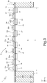
- Figure 3 illustrates the actuator 1 of Figure 2 in lateral cross-sectional view, in the plane XZ, taken along the line of section III-III of Figure 2 .
- each piezoelectric band 50a-50k comprises, in one embodiment, a stack formed by a first electrode 51 (made, for example, of Pt), a layer of piezoelectric material 52 (made, for example, of PZT), and a second electrode 53 (made, for example, of TiW).
- An insulating layer 56 e.g., SiO 2 ) extends underneath the respective stack 51-53.
- Each piezoelectric band 50a-50k may thus be represented electrically as a capacitor, the first electrode 51 of which is connected to ground and the second electrode 52 of which is biased in the way described hereinafter.
- Figure 4A represents, in particular, the piezoelectric bands 50a, 50c, 50e, 50g, 50i, 50j.
- the stack 51-53 extends over the insulating layer 56, which, in turn, extends over the base supporting layer 2'; on an opposite face of the base supporting layer 2', extending in a region corresponding to the stack 51-53 is a thickness-increase layer 57, made, for example, of polysilicon.
- the thickness, measured along the axis Z, of the thickness-increase layer 57, in the case where it is made of polysilicon, is, for example, 4 ⁇ m. Other materials, different from polysilicon, may be used.
- the thickness is chosen according to the desired stiffness, the latter being a function of the ratio between Young's modulus and the thickness of the material used.
- the desired stiffness for the thickness-increase layer 57 is between 100 kPa ⁇ m and 1600 kPa ⁇ m.
- Figure 4B represents, instead, the piezoelectric bands 50b, 50d, 50f, 50h, 50k.
- the respective stack 51-53 extends over the base supporting layer 2' and the insulating layer 56 and is covered by a thickness-increase layer 58, made, for example, of silicon nitride.
- the thickness, measured along the axis Z, of the thickness-increase layer 58, in the case where it is made of silicon nitride, is, for example, 3 ⁇ m. Other materials, different from silicon nitride, may be used.
- the thickness is chosen according to the desired stiffness for the thickness-increase layer 58. In general, the desired stiffness for the thickness-increase layer 58 is between 100 kPa ⁇ m and 1600 kPa ⁇ m.
- a respective sub-portion 38b, 39b, 40b, 41b, and 47c carries a respective piezoelectric band 50b, 50d, 50f, 50h, 50k of the type illustrated in Figure 4A that is provided with the silicon-nitride structural layer 58 but without the polysilicon structural layer 57.
- a respective sub-portion 38a, 39a, 40a, 41a, and 47a-47b carries a respective piezoelectric band 50a, 50c, 50e, 50g, 50i-50j of the type illustrated in Figure 4B that is without the silicon-nitride structural layer 58 but is provided with the polysilicon structural layer 57.
- the piezoelectric bands 50a, 50b, 50c, and 50d have a main extension L P1 , along the axis Y, equal to approximately one half of the extension, along the axis Y, of the corresponding sub-portion 38a, 38b, 39a, 39b to which they are coupled (i.e., equal to L Y /2).
- Each piezoelectric band 50a, 50b, 50c and 50d is symmetrical with respect to the axis of symmetry A.
- the value of L P1 is 1300 ⁇ m.
- the piezoelectric bands 50e, 50f, 50h, and 50g have a main extension L P2 , along the axis Y, equal to approximately one half of the extension, along the axis Y, of the corresponding sub-portion 40a, 40b, 41a, 41b to which they are coupled.
- Each piezoelectric band 50e, 50f, 50h, and 50g is symmetrical with respect to the axis of symmetry A.
- the value of L P2 is 1000 ⁇ m.
- the piezoelectric bands 50i, 50k, and 50j have a main extension L P3 , along the axis Y, equal to approximately one half of the extension, along the axis Y, of the corresponding sub-portion 47a, 4cb, 47b to which they are coupled.
- Each piezoelectric band 50i, 50k, and 50j is symmetrical with respect to the axis of symmetry A.
- the value of L P3 is 800 ⁇ m.
- the piezoelectric bands 50a, 50c, 50e, 50g, 50i, 50j are electrically connected to a first voltage generator 76, and the piezoelectric bands 50b, 50d, 50f, 50h, 50k are electrically connected to a second voltage generator 77 via metal connections illustrated only schematically in Figures 4A and 4B in so far as they are in themselves of a known type.
- the voltage generators 76 and 77 may, in one embodiment, coincide with one another.
- the voltage generators 76 and 77 are configured to bias the piezoelectric bands at a working voltage, for example comprised between 0 V and 80 V.
- the working voltage is, in particular, of a unipolar or unidirectional type (i.e., the working voltage is always comprised between zero and the maximum positive or negative voltage; in other words, the supply signal assumes, in time, only negative voltage values or, alternatively, only positive voltage values).
- Figure 5A shows schematically, in perspective view, the actuator 1 during an operating condition
- Figure 5B is an enlarged view of the portion represented circled in Figure 5A .
- the stress induced by the electrical field in the PZT generates a concave or convex deflection in the sub-portions 38a-47c that is a function of the presence/absence of the thickness-increase layers 57 and 58.
- the piezoelectric bands 50b, 50d, 50f, 50h, 50k generate, in the silicon-nitride layer 58, a tensile stress that, transmitted by the thickness-increase layer 58 to the insulating layer 56 and to the base support 2', causes a downward bending, also conventionally referred to as "positive bending", of the respective sub-portions 38b, 39b, 40b, 41b, and 47c.
- the piezoelectric bands 50a, 50c, 50e, 50g, 50i-50j generate, in the thickness-increase layer 57, a compressive stress that causes an upward bending, also conventionally referred to as "negative bending", of the respective sub-portions 38a, 39a, 40a, 41a, and 47a-47b.
- the positive bending of the sub-portions 38a and 39a causes a displacement, or translation, of the connection arms 18a' and 18b' in the positive direction of the axis Z (i.e., away from the cavity 6). Since the sub-portions 38b, 39b are constrained to the connection arms 18a' and 18b', they will undergo a similar displacement in the positive direction of the axis Z.
- the sub-portions 38b, 39b undergo a negative bending that causes a further displacement, or translation, in the positive direction of the axis Z (i.e., away from the cavity 6), of their portions comprised between the connection arms 18a' and 18b'.
- the maximum displacement is obtained at the centroid of the sub-portions 38b, 39b, i.e., in a position corresponding to the axis of symmetry A.
- sub-portions 40a-40b and 41a-41b are subjected to a bending similar to the one described for the sub-portions 38a-38b and 39a-39b, respectively.
- the coupling elements 26, 27 constrain the sub-portions 40b, 41b to the arm 22, the latter is subjected to a displacement, in the positive direction of the axis Z, equal to the sum of the displacements of the sub-portion 38a, of the sub-portion 38b, of the sub-portion 40a, and of the sub-portion 40b (corresponding to the sum of the displacements of the sub-portion 39a, of the sub-portion 39b, of the sub-portion 41a, and of the sub-portion 41b).
- sub-portions 47a and 47b are subjected to a bending similar to the one described for the sub-portions 38a, 39a, 40a, and 41a
- sub-portion 47c is subjected to a bending similar to the one described for the sub-portions 38b, 40b, 39b, and 41b.
- the voltage generators 76, 77 are phase-controlled.
- an actuation voltage is applied, in particular of a unipolar type, to the piezoelectric bands 50a-50k comprised between 0 V (deformable structure 2 in the resting condition) and 40 V (deformable structure 2 in a condition of maximum extension along the axis Z).
- the actuation arms undergo deformation and bend, and the bending is all the more accentuated, the higher the voltage applied to the piezoelectric bands 50a-50k.
- each sub-portion 38a, 39a40a, 41a, 47c increases as the latter move away from the supporting and coupling/anchorage elements 12, 14, 23-27, up to a maximum of 10° at the connection arms 18a', 18b', 20a', 20b'.
- the actuator 1 finds application, for example, in a speaker 101 for use in a portable electronic apparatus 100, as illustrated in Figure 8 .
- the speaker 101 integrates the actuator 1, which, when actuated, has the function of displacing a diaphragm in order to generate an acoustic wave.
- a driving circuit 102 is configured to supply the operating voltage necessary for biasing the piezoelectrics, for actuation of the actuator 1 according to what has been described previously.
- actuator device for a telescopic type, or miniature elevators
- height micro-positioners mechanical micro-elevators or nano-elevators (of a telescopic type, or miniature elevators)
- micro-contactors between two contacts with a certain gap along the axis Z and the like.
- the actuator device 1 described herein presents numerous advantages.
- the present invention makes it possible to obtain, in use, a marked displacement of an actuation portion (here, the sub-portion 47c) with respect to a resting condition thereof.
- the total displacement is given by a sum of local displacements.
- the present invention enables reduction of the consumption of area as compared to a membrane actuator of a known type.
- the first functional sub-structure 18 is not present.
- the second functional sub-structure 20 is mechanically coupled to the frame 4 by supporting elements 80, 81 similar to the supporting elements 12, 14.
- the through trench 30 extends, in this case, between the frame 4 and the second functional sub-structure 20 except for the regions in which the supporting elements 80, 81 are present.
- the second functional sub-structure 20 is thus constrained to the frame 4 exclusively in a position corresponding to the supporting elements 80, 81, and is otherwise free to move with respect to the frame 4.
- the third functional sub-structure 22 is mechanically coupled to the frame 4 by supporting elements 82, 84 similar to the supporting elements 12, 14.
- the through trench 30 extends, in this case, between the frame 4 and the third functional sub-structure 22 except for the regions in which the supporting elements 82, 84 are present.
- the third functional sub-structure 22 is thus constrained to the frame 4 exclusively at the supporting elements 82, 84, and is otherwise free to move with respect to the frame 4.
- further functional sub-structures may be present similar to the functional sub-structure 18 or 20 (i.e., having a similar shape and comprising the same mechanical elements and the actuation piezoelectrics), said further functional sub-structures extending between the frame 4 and the functional sub-structure 18 and/or between the functional sub-structure 18 and the functional sub-structure 20 and/or between the functional sub-structure 20 and the functional sub-structure 22.
Landscapes
- Engineering & Computer Science (AREA)
- Microelectronics & Electronic Packaging (AREA)
- Computer Hardware Design (AREA)
- Physics & Mathematics (AREA)
- Acoustics & Sound (AREA)
- Signal Processing (AREA)
- Manufacturing & Machinery (AREA)
- Micromachines (AREA)
Abstract
Description
- The present invention relates to an actuator device based upon piezoelectric technology and to an apparatus, in particular a speaker, that comprises the actuator device. In particular, reference will be made hereinafter to an actuator obtained in MEMS (Micro-Electro-Mechanical System) technology.
- Micromechanical actuators are known having a membrane structure, which is obtained with the technology of semiconductor materials. The membrane, provided with one or more piezoelectric elements, is made to deflect in a driving direction by appropriately controlling the piezoelectric elements. The mechanical deformation of the membrane has a specific utility according to the application in which it is used. For instance, in fluidic applications, the membrane may form part of a micropump or a printhead, and its deflection may be used to cause displacement of a mass of fluid.
- Other applications of micromechanical actuators include, for example, the acoustic field. Piezoeletrically actuated membranes are, for example, used in miniaturized speakers that are integrated, for example, in portable apparatuses, such as portable computers, laptops, notebooks (including the ultra-thin notebooks), PDAs, tablets, and smartphones.
- Thanks to the small dimensions, said devices make it possible to respect stringent requirements as regards occupation of space, in terms of area and thickness.
- The present applicant has found that, frequently, the deflection required of membranes of actuators of a known type is of several hundreds of micrometres (500-2000 µm) in a direction orthogonal to the plane of lie of the membrane itself (out-of-plane deflection). This performance may be obtained by increasing the area of the membrane, at the expense of occupation of space.
- The aim of the present invention is to provide a micro-electro-mechanical device with actuation of piezoelectric type that will overcome the drawbacks of the prior art.
- According to the present invention, an actuator device and an apparatus that comprises the micro-electro-mechanic actuator device are provided, as defined in the annexed claims.
- For a better understanding of the present invention, a preferred embodiment thereof is now described, purely by way of non-limiting example, with reference to the attached drawings, wherein:
-
Figure 1 illustrates, in top plan view, a MEMS actuator according to an aspect of the present invention; -
Figure 2 illustrates, in top plan view, the MEMS actuator ofFigure 1 according to a further aspect of the present invention; -
Figure 3 illustrates, in lateral cross-sectional view, the MEMS actuator ofFigure 2 ; -
Figures 4A and 4B illustrate, with a higher degree of detail, portions of the MEMS actuator ofFigure 3 ; -
Figure 5A illustrates, in perspective view, the MEMS actuator according to the present invention, in use; -
Figure 5B illustrates an enlarged detail of the MEMS actuator ofFigure 5A ; -
Figure 6 illustrates a MEMS actuator according to a further embodiment of the present invention; -
Figure 7 illustrates a MEMS actuator according to a further embodiment of the present invention; and -
Figure 8 illustrates an apparatus that comprises a MEMS actuator according to any embodiment of the present invention. -
Figure 1 illustrates a portion of anactuator 1, of a micro-electro-mechanical type, in a triaxial reference system, with mutually orthogonal axes X, Y, Z. In particular,Figure 1 illustrates theactuator 1 in top view in the plane XY, according to an embodiment of the present invention. - The
actuator 1 is provided with adeformable structure 2, designed to bend in the direction of the axis Z, orthogonal to the plane XY. Thedeformable structure 2 is supported by aframe 4, of a fixed type, which surrounds thedeformable structure 2 completely. In a different embodiment, not illustrated, theframe 4 may surround thedeformable structure 2 only partially. - As may be seen in
Figure 3 , described more fully in what follows, thedeformable structure 2 is suspended over acavity 6 obtained, for example, by digging asubstrate 8 using micromachining techniques of a per se known type. Thedeformable structure 2 extends, in this embodiment, on afront side 8a of thesubstrate 8. - In the context of the present invention, it is irrelevant whether the
substrate 8 is a monolithic block or else is formed by a plurality of regions or layers arranged on top of one another (e.g., layers grown epitaxially). Thesubstrate 8 may include one or more semiconductor and/or insulating materials. Theframe 4 may be integrated in thesubstrate 8, or else be formed by thesubstrate 8 itself. - The
frame 4 is mechanically coupled to thedeformable structure 2 by a first supporting element, or constraint, 12 and a second supporting element, or constraint, 14, which have a shape and size substantially the same as one another and are aligned to one another in a direction parallel to the axis X. In one embodiment, the first supportingelement 12 and the second supportingelement 14 lie, both in a resting condition and in an operating condition (the latter being illustrated more fully in what follows), in one and the same plane parallel to the plane XY. - The first and second supporting
elements frame 4. - By way of example, the
frame 4 has a quadrangular shape, with extension along the axis X of approximately 2 mm and extension along the axis Y of approximately 2 mm. The first and second supportingelements - The thickness, along the axis Z, of the first and second supporting
elements - In one embodiment, the
frame 4 includes, for example, a layer of (monocrystalline or polycrystalline) silicon, deposited or grown on thefront side 8a of thesubstrate 8; it is evident that other materials may be used, in addition to or instead of silicon. - The above layer of (monocrystalline or polycrystalline) silicon, deposited or grown on the
front side 8a of thesubstrate 8 likewise forms, according to an embodiment, a base supporting layer 2' that defines the shape of the deformable structure 2 (see, for example,Figure 3 ). - The thickness, measured along the axis Z, of the base supporting layer 2' is, for example, between 0.5 µm and 20 µm.
- In one embodiment, the
frame 4, the first and second supportingelements deformable structure 2 are made of a single piece and, in the resting condition, lie in one and the same plane (here, the plane XY). - The
deformable structure 2 and the supportingframe 4 may be obtained starting from a wafer of semiconductor material, for example silicon, using known semiconductor-machining techniques, such as digging, growth, deposition, and/or selective removal, in a per se known manner. - The
deformable structure 2 here has a quadrangular shape, in particular rectangular with a major side Ly along the axis Y and a minor side Lx along the axis X. For instance, the major side Ly is 2.5 mm, and the minor side Lx is 2 mm. - The
deformable structure 2 is further symmetrical both with respect to an axis of symmetry A, parallel to the axis X and passing through a geometrical centre O of a rectangle of sides LY and LX that defines the outer edges of thedeformable structure 2, and with respect to an axis of symmetry B, parallel to the axis Y and passing through the geometrical centre O. The first and second supportingelements - The
deformable structure 2 comprises a firstfunctional sub-structure 18, a secondfunctional sub-structure 20, and a thirdfunctional sub-structure 22. The first, second, and thirdfunctional sub-structures functional sub-structures - The first, second, and third
functional sub-structures constraint elements coupling elements functional sub-structure 18 to the secondfunctional sub-structure 20 and extend symmetrically with respect to the axis of symmetry B and are aligned along the first axis of symmetry A (along the axis X). Thecoupling elements elements coupling elements functional sub-structure 20 to the thirdfunctional sub-structure 22 and extend symmetrically to one another with respect to the axis of symmetry B, and are aligned, along the first axis of symmetry A, to the first and second supportingelements coupling elements - In other words, the
frame 4 and the first, second, and thirdfunctional sub-structures frame 4 surrounds completely, in view in the plane XY, the firstfunctional sub-structure 18; the firstfunctional sub-structure 18 surrounds completely, in view in the plane XY, the secondfunctional sub-structure 20; and the secondfunctional sub-structure 20 surrounds completely, in view in the plane XY, the thirdfunctional sub-structure 22. The first, second, and thirdfunctional sub-structures cavity 6 by the first and second supportingelements coupling elements - It may further be noted that the
frame 4 is separated from the firstfunctional sub-structure 18 by a first throughtrench 30, which extends along the axis Z throughout the thickness of thedeformable structure 2 and extends, in the plane XY, between theframe 4 and the firstfunctional sub-structure 18 except for the constraint regions provided by the first and second supportingelements - The second
functional sub-structure 20 is separated from the firstfunctional sub-structure 18 by a second throughtrench 32, which extends between the first and secondfunctional sub-structures coupling elements - The third
functional sub-structure 22 is separated from the secondfunctional sub-structure 20 by a third throughtrench 34, which extends between the second and thirdfunctional sub-structures coupling elements - In detail, the first, second, and third
functional sub-structures reference numbers actuation arm 18a is symmetrical, with respect to the axis of symmetry B, to theactuation arm 18b; theactuation arm 20a is symmetrical, with respect to the axis of symmetry B, to theactuation arm 20b; finally, theactuation arm 22a extends along the axis of symmetry B and comprises the geometrical centre O of thedeformable structure 2. Observed with respect to the axis of symmetry B, also theactuation arm 22a is symmetrical. - Each of the first, second, and third
functional sub-structures reference numbers 18a', 18b'; 20a', 20b', which extend in a direction transverse to theactuation arms connection arms 18a', 18b', 20a', 20b' are mutually parallel and have a direction of main extension along the axis X. Theconnection arms 18a' and 18b' are mechanically coupled to theactuation arms actuation arms connection arm 18a' mechanically connects one end of theactuation arm 18a to a respective end of theactuation arm 18b, while theconnection arm 18b' mechanically connects the other end of theactuation arm 18a to another respective end of theactuation arm 18b. - The
connection arms 20a' and 20b' are mechanically coupled to theactuation arms arms - The
connection arms 18a' and 20a' are symmetrical to theconnection arms 18b', 20b', respectively, when they are considered with respect to the axis of symmetry A. - It is evident that, in one embodiment, the connection arms extend as a prolongation of the ends of the actuation arms to which they are coupled without any discontinuity (i.e., without any solution of continuity); for example, they are formed in a common layer of material and by manufacturing steps that are at least in part in common.
- According to a further aspect of the present invention, the
actuation arm 18a has a throughtrench 36, which extends along the axis Z throughout the thickness of theactuation arm 18a, and has a direction of main extension parallel to the axis Y; the throughtrench 36 divides thearm 18a into twosub-portions sub-portion 38a may bend in the negative direction of the axis Z, and at the same time the sub-portion 38b may bend in the positive direction of the axis Z). - The
actuation arm 18b is similar to theactuation arm 18a, and has a respective throughtrench 37 that extends along the axis Z throughout the thickness of theactuation arm 18b, and has a direction of main extension parallel to the direction of the axis Y; the throughtrench 37 divides thearm 18b into twosub-portions sub-portion 39a may bend in the negative direction of the axis Z, and at the same time the sub-portion 39b may bend in the positive direction of the axis Z). - As described above, the
actuation arm 20a has a throughtrench 42 that extends along the axis Z throughout the thickness of theactuation arm 20a, and has a direction of main extension parallel to the direction of the axis Y; the throughtrench 42 divides thearm 20a into twosub-portions sub-portion 40a may bend in the negative direction of the axis Z, and at the same time the sub-portion 40b may bend in the positive direction of the axis Z). - The
arm 20b is similar to thearm 20a, and has a respective throughtrench 43 that extends along the axis Z throughout the thickness of theactuation arm 20b and has a direction of main extension parallel to the direction of the axis Y; the throughtrench 43 divides thearm 20b into twosub-portions sub-portion 41a may bend in the negative direction of the axis Z, and at the same time the sub-portion 41b may bend in the positive direction of the axis Z). - The
actuation arm 22 has two throughtrenches actuation arm 22 and have a direction of main extension parallel to the direction of the axis Y; the throughtrenches arm 22 into threesub-portions sub-portion 47c may bend in the positive direction of the axis Z). - As illustrated in
Figure 2 , each of the sub-portions 38a, 38b, 39a, 39b, 40a, 40b, 41a, 41b, 47a-47c carries arespective actuation band 50a-50k, of piezoelectric material (in what follows, also referred to as "piezoelectric band"). -
Figure 3 illustrates theactuator 1 ofFigure 2 in lateral cross-sectional view, in the plane XZ, taken along the line of section III-III ofFigure 2 . - As illustrated in
Figures 4A and 4B , eachpiezoelectric band 50a-50k comprises, in one embodiment, a stack formed by a first electrode 51 (made, for example, of Pt), a layer of piezoelectric material 52 (made, for example, of PZT), and a second electrode 53 (made, for example, of TiW). An insulating layer 56 (e.g., SiO2) extends underneath the respective stack 51-53. Eachpiezoelectric band 50a-50k may thus be represented electrically as a capacitor, thefirst electrode 51 of which is connected to ground and thesecond electrode 52 of which is biased in the way described hereinafter. -
Figure 4A represents, in particular, thepiezoelectric bands layer 56, which, in turn, extends over the base supporting layer 2'; on an opposite face of the base supporting layer 2', extending in a region corresponding to the stack 51-53 is a thickness-increase layer 57, made, for example, of polysilicon. The thickness, measured along the axis Z, of the thickness-increase layer 57, in the case where it is made of polysilicon, is, for example, 4 µm. Other materials, different from polysilicon, may be used. In this case, the thickness is chosen according to the desired stiffness, the latter being a function of the ratio between Young's modulus and the thickness of the material used. In general, the desired stiffness for the thickness-increase layer 57 is between 100 kPa·m and 1600 kPa·m. -
Figure 4B represents, instead, thepiezoelectric bands layer 56 and is covered by a thickness-increase layer 58, made, for example, of silicon nitride. The thickness, measured along the axis Z, of the thickness-increase layer 58, in the case where it is made of silicon nitride, is, for example, 3 µm. Other materials, different from silicon nitride, may be used. In this case, the thickness is chosen according to the desired stiffness for the thickness-increase layer 58. In general, the desired stiffness for the thickness-increase layer 58 is between 100 kPa·m and 1600 kPa·m. - From what has been described above, it follows that for each
arm respective sub-portion piezoelectric band Figure 4A that is provided with the silicon-nitridestructural layer 58 but without the polysiliconstructural layer 57. Further, for eacharm respective sub-portion piezoelectric band Figure 4B that is without the silicon-nitridestructural layer 58 but is provided with the polysiliconstructural layer 57. - The
piezoelectric bands corresponding sub-portion piezoelectric band - The
piezoelectric bands corresponding sub-portion piezoelectric band - The
piezoelectric bands corresponding sub-portion 47a, 4cb, 47b to which they are coupled. Eachpiezoelectric band - The
piezoelectric bands first voltage generator 76, and thepiezoelectric bands second voltage generator 77 via metal connections illustrated only schematically inFigures 4A and 4B in so far as they are in themselves of a known type. Thevoltage generators voltage generators -
Figure 5A shows schematically, in perspective view, theactuator 1 during an operating condition;Figure 5B is an enlarged view of the portion represented circled inFigure 5A . - As may be noted from
Figures 5A and 5B , when thepiezoelectric bands 50a-50k are biased at the working voltage, they induce a stress in the sub-portions 38a-47c of thearms 18a-22a to which they are coupled, which consequently generates bending of the sub-portions 38a-47c themselves. - The stress induced by the electrical field in the PZT generates a concave or convex deflection in the sub-portions 38a-47c that is a function of the presence/absence of the thickness-
increase layers piezoelectric bands nitride layer 58, a tensile stress that, transmitted by the thickness-increase layer 58 to the insulatinglayer 56 and to the base support 2', causes a downward bending, also conventionally referred to as "positive bending", of therespective sub-portions piezoelectric bands increase layer 57, a compressive stress that causes an upward bending, also conventionally referred to as "negative bending", of therespective sub-portions - As a result of the fact that the
deformable structure 2 is constrained to theframe 4 exclusively by the first and second supportingelements connection arms 18a' and 18b' in the positive direction of the axis Z (i.e., away from the cavity 6). Since the sub-portions 38b, 39b are constrained to theconnection arms 18a' and 18b', they will undergo a similar displacement in the positive direction of the axis Z. Further, as a result of the biasing of thepiezoelectric bands connection arms 18a' and 18b'. The maximum displacement is obtained at the centroid of the sub-portions 38b, 39b, i.e., in a position corresponding to the axis of symmetry A. - Since the
coupling elements actuation arms sub-portion 38a (respectively 39a) and of the sub-portion 38b (respectively 39b). - In turn, the sub-portions 40a-40b and 41a-41b, are subjected to a bending similar to the one described for the sub-portions 38a-38b and 39a-39b, respectively.
- Since the
coupling elements arm 22, the latter is subjected to a displacement, in the positive direction of the axis Z, equal to the sum of the displacements of thesub-portion 38a, of the sub-portion 38b, of thesub-portion 40a, and of the sub-portion 40b (corresponding to the sum of the displacements of thesub-portion 39a, of the sub-portion 39b, of thesub-portion 41a, and of the sub-portion 41b). - In turn, the sub-portions 47a and 47b are subjected to a bending similar to the one described for the sub-portions 38a, 39a, 40a, and 41a, while the sub-portion 47c is subjected to a bending similar to the one described for the sub-portions 38b, 40b, 39b, and 41b.
- There is thus obtained an effective displacement of the sub-portion 47c in the positive direction of the axis Z equal to the sum of the displacements of the sub-portions 38a, 38b, 40a, 40b, and 47a (equivalent to the sum of the displacements of the sub-portions 39a, 39b, 41a, 41b, and 47b) with respect to a resting condition of lie in the plane XY.
- In use, the
voltage generators piezoelectric bands 50a-50k comprised between 0 V (deformable structure 2 in the resting condition) and 40 V (deformable structure 2 in a condition of maximum extension along the axis Z). As indicated above, in these conditions, the actuation arms undergo deformation and bend, and the bending is all the more accentuated, the higher the voltage applied to thepiezoelectric bands 50a-50k. - As illustrated in
Figures 5A and 5B , the angle of deflection (measured with respect to the plane XY) of each sub-portion 38a, 39a40a, 41a, 47c increases as the latter move away from the supporting and coupling/anchorage elements connection arms 18a', 18b', 20a', 20b'. - The
actuator 1 according to the present invention finds application, for example, in aspeaker 101 for use in a portableelectronic apparatus 100, as illustrated inFigure 8 . Thespeaker 101 integrates theactuator 1, which, when actuated, has the function of displacing a diaphragm in order to generate an acoustic wave. A drivingcircuit 102 is configured to supply the operating voltage necessary for biasing the piezoelectrics, for actuation of theactuator 1 according to what has been described previously. - Other applications of the actuator device according to the present invention regard height micro-positioners, mechanical micro-elevators or nano-elevators (of a telescopic type, or miniature elevators), micro-contactors between two contacts with a certain gap along the axis Z, and the like.
- The
actuator device 1 described herein presents numerous advantages. In particular, the present invention makes it possible to obtain, in use, a marked displacement of an actuation portion (here, the sub-portion 47c) with respect to a resting condition thereof. The total displacement is given by a sum of local displacements. Given the same maximum height reached by the actuation portion, the present invention enables reduction of the consumption of area as compared to a membrane actuator of a known type. - Finally, it is clear that modifications and variations may be made to the microelectronic device described and illustrated herein, without thereby departing from the scopeof the present invention, as defined in the annexed claims.
- For instance, as illustrated in
Figure 6 , in anactuator 85 according to a further embodiment of the present invention, the firstfunctional sub-structure 18 is not present. In this case, the secondfunctional sub-structure 20 is mechanically coupled to theframe 4 by supportingelements elements trench 30 extends, in this case, between theframe 4 and the secondfunctional sub-structure 20 except for the regions in which the supportingelements functional sub-structure 20 is thus constrained to theframe 4 exclusively in a position corresponding to the supportingelements frame 4. The remaining technical characteristics, as likewise the operating principle, are in accordance with the ones already described with reference to the foregoing figures and the respective embodiments, and are thus not described any further herein for reasons of brevity. - In an
actuator 95 according to a further embodiment of the present invention (illustrated inFigure 7 ), neither the firstfunctional sub-structure 18 nor the secondfunctional sub-structure 20 are present. In this case, the thirdfunctional sub-structure 22 is mechanically coupled to theframe 4 by supportingelements elements trench 30 extends, in this case, between theframe 4 and the thirdfunctional sub-structure 22 except for the regions in which the supportingelements functional sub-structure 22 is thus constrained to theframe 4 exclusively at the supportingelements frame 4. The remaining technical characteristics, as likewise the operating principle, are in accordance with the ones already described with reference to the foregoing figures and the respective embodiments, and thus are not described any further herein for reasons of brevity. - In a further embodiment (not illustrated in the figures), further functional sub-structures may be present similar to the
functional sub-structure 18 or 20 (i.e., having a similar shape and comprising the same mechanical elements and the actuation piezoelectrics), said further functional sub-structures extending between theframe 4 and thefunctional sub-structure 18 and/or between thefunctional sub-structure 18 and thefunctional sub-structure 20 and/or between thefunctional sub-structure 20 and thefunctional sub-structure 22. - Further, the examples indicated previously with reference to the dimensions, materials, and voltages for controlling the piezoelectrics are to be deemed as purely indicative of a possible non-limiting embodiment of the present invention. Variations in shape, materials, dimensions, and control voltages are possible and within the reach of the person skilled in the art on the basis of the teachings of the present disclosure.
Claims (21)
- A micro-electro-mechanic actuator device (1; 85; 95) comprising:- a fixed structure (4); and- a mobile structure (2) configured to move along a driving direction (Z) and includes a first deformable band (47c), a second deformable band (47a) and a third deformable band (47b) which lie, in a first operating condition, in a resting plane (XY) and have a respective main extension along a first direction (Y) orthogonal to the driving direction (Z), the first deformable band (47c) being arranged between the second and third deformable bands (47a, 47b) and being mechanically uncoupled, along said first direction (Y), from the second and third deformable bands (47a, 47b) by respective first and second through trenches,the first, second, and third deformable bands (47c, 47a, 47b) each having respective ends and being joined together at said ends,
and wherein the second deformable band (47a) is further coupled to the fixed structure (4) by a first supporting element (12; 80; 82), and the third deformable band (47b) is coupled to the fixed structure (4) by a second supporting element (14; 81; 84), the first and second supporting elements being aligned to one another, at least in the first operating condition, along one and a same first axis of symmetry (A) orthogonal to said first direction (Y),
the first, second, and third deformable bands (47c, 47a, 47b) housing first, second, and third piezoelectrics (50k, 50i, 50j), respectively,
wherein the second and third deformable bands (47a, 47b) and the respective second and third piezoelectrics (50i, 50j) are arranged with respect to one another and configured so that, in a second operating condition where the second and third piezoelectrics are biased by a working voltage, the second and third deformable bands (47a, 47b) are subjected to a negative bending that causes a translation of said ends and of the first deformable band (47c) in said driving direction (Z);
the first deformable band (47c) and the respective first piezoelectric being arranged with respect to one another and configured so that, when the first piezoelectric is biased at the working voltage, the first deformable band (47c) is subjected to a positive bending that causes a further translation in said driving direction (Z) of at least one portion of the first deformable band (47c), which extends between said ends of the first deformable band. - The actuator device according to claim 1, wherein the translation of said ends and of the first deformable band (47c) and said further translation of at least one portion of the first deformable band (47c) are directed with the same orientation as that of said driving direction (Z), adding to one another.
- The actuator device according to claim 1 or claim 2, wherein the first, second, and third piezoelectrics (50i, 50j) extend at respective first sides of the first, second, and third deformable bands,
said mobile structure (2) further comprising: a first thickness-increase region (58) at the first side of the first deformable band (47c) above the first piezoelectric (50k); a second thickness-increase region (57) at a second side, opposite to the first side in the driving direction (Z), of the second deformable band (47a); and a third thickness-increase region (57) at a respective second side, opposite to the respective first side in the driving direction (Z), of the third deformable band (47a). - The actuator device according to claim 3, wherein the first thickness-increase region (58) has a thickness, in the driving direction (Z), comprised between 0.2 µm and 20 µm.
- The actuator device according to claim 3 or claim 4, wherein the second and third thickness-increase regions (58) have a same thickness, in the driving direction (Z), comprised between 0.2 µm and 20 µm.
- The actuator device according to any one of claims 3-5, wherein the first, second, and third thickness-increase regions (57) have an extension, in the first direction (Y), equal to or greater than the respective extension of the first, second, and third piezoelectrics.
- The actuator device according to any one of claims 3-6, wherein the first thickness-increase region (58) is made of silicon nitride.
- The actuator device according to any one of claims 3-7, wherein the second and third thickness-increase regions (57) are both of polysilicon.
- The actuator device according to any one of the preceding claims, wherein said fixed structure (4) extends alongside said mobile structure (2) and at a distance from the mobile structure (2) so that the fixed structure (4) and the mobile structure (2) are mechanically uncoupled from one another except for the regions connected to said first and second supporting elements (12, 14; 82, 84).
- The actuator device according to any one of the preceding claims, wherein said mobile structure (2) is a suspended platform carried by said fixed structure (4), said first and second supporting elements (12, 14; 82, 84) forming a rigid suspension structure lying, both in the first operating condition and in the second operating condition, in the resting plane (XY).
- The actuator device according to any one of the preceding claims, wherein the mobile structure (2) is suspended over a cavity (6) formed in a body (8) of semiconductor material forming, at least in part, said fixed structure (4).
- The actuator device according to any one of the preceding claims, wherein the first, second, and third deformable bands (47a-47c) have, in view in the resting plane (XY), a rectangular shape with a major side along the first direction (Y) and a minor side along a second direction (X) orthogonal to the first direction (Y) and to the driving direction (Z),
and wherein the first, second, and third piezoelectrics have, in view in the resting plane (XY), a rectangular shape with a major side along the first direction (Y) of a length equal to half of the major side than the first, second, and third deformable bands,
and wherein the geometrical centres of the first, second, and third deformable bands coincide with the respective geometrical centres of the first, second, and third piezoelectrics. - The actuator device according to claim 12, wherein the geometrical centres of the first, second, and third deformable bands and of the first, second, and third piezoelectrics are aligned with respect to one another along said first axis of symmetry (A).
- The actuator device according to claim 12 or claim 13, wherein said mobile structure (2) is further symmetrical both with respect to the first axis of symmetry (A) and with respect to a second axis of symmetry (B) parallel to said first direction (Y) and passing through the geometrical centre of the first deformable band (47c).
- The actuator device according to any one of the preceding claims, wherein the mobile structure (2) further comprises: a fourth deformable band (40a) and a fifth deformable band (40b), which lie in the resting plane (XY) and have a respective main extension in the first direction (Y), and are arranged between the second deformable band (47a) and the first supporting element (12; 80), mechanically uncoupled from one another, in said first direction (Y), by a third through trench; and a sixth deformable band (41a) and a seventh deformable band (41b), which lie in the resting plane (XY) and have a respective main extension in the first direction (Y), and are arranged between the third deformable band (47b) and the second supporting element (14; 81), mechanically uncoupled from one another, in said first direction (Y), by a fourth through trench,
wherein the fourth, fifth, sixth, and seventh deformable bands (40a, 40b, 41a, 41b) are mechanically coupled together, at respective first ends, by a first connection arm (20a') and, at respective second ends, by a second connection arm (20b'),
wherein the fifth deformable band (40b) extends at a distance from, and directly faces, the second deformable band (47a), and is mechanically coupled to the second deformable band by a coupling element (26), while the fourth deformable band (40b) is mechanically coupled to the fixed structure (4) by the first supporting element (12; 80),
and wherein the seventh deformable band (41b) extends at a distance from, and directly faces, the third deformable band (47b) and is mechanically coupled to the third deformable band by a coupling element (227), while the sixth (41a) deformable band is mechanically coupled to the fixed structure (4) by the second supporting element (14; 81),
and wherein the fourth, fifth, sixth, and seventh deformable bands (40a, 40b, 41a, 41b) house a fourth piezoelectric (50e), a fifth piezoelectric (50f), a piezoelectric (50g) sixth, and a seventh piezoelectric (50h), respectively. - The actuator device according to claim 15, wherein the fourth and sixth deformable bands (40a, 41a) and the respective fourth and sixth piezoelectrics (50e, 50g) are aranged with respect to one another and configured so that, in the second operating condition where the fourth and sixth piezoelectrics are biased at the working voltage, the fourth and sixth deformable bands (40a, 41a) are subjected to a negative bending that causes translation of the first and second connection arms (20a', 20b') and of the fifth and seventh deformable bands (40b, 41b) in said driving direction (Z),
and wherein the fifth and seventh deformable bands (40b, 41b) and the respective fifth and seventh piezoelectrics (50f, 50h) are arranged with respect to one another and configured so that, in the second operating condition where the fifth and seventh piezoelectrics are biased at the working voltage, the fifth and seventh deformable bands (40b, 41b) are subjected to a positive bending that causes a further translation in said driving direction (Z) of portions of the fifth and seventh deformable bands (40b, 41b) that extend between the first and second connection arms (20a', 20b'). - The actuator device according to claim 15 or claim 16, wherein the first and second connection arms (20a', 20b') are mutually parallel and symmetrical with respect to said first axis of symmetry (A).
- The actuator device according to any one of the preceding claims, wherein the first, second, and third piezoelectrics (50k, 50i, 50j) are electrically coupled to a voltage generator (76, 77).
- The actuator device according to claim 18, wherein the voltage generator (76, 77) is configured to bias the first, second, and third piezoelectrics (50k, 50i, 50j) to a zero operating voltage in the first operating condition and to an operating voltage comprised between 0 V and 50 V in the second operating condition.
- An apparatus (101) for use in a portable electronic device (100), comprising the actuator device (1; 85; 95) according to any one of claims 1-19; and
a driving circuit (102) configured to supply said operating voltage to the first, second, and third piezoelectrics. - The apparatus according to claim 20, chosen in the group comprising: a speaker, a micro-positioner, a micro-elevator or nano-elevator, or a micro-contactor.
Applications Claiming Priority (1)
| Application Number | Priority Date | Filing Date | Title |
|---|---|---|---|
| IT201700135836 | 2017-11-27 |
Publications (2)
| Publication Number | Publication Date |
|---|---|
| EP3490018A1 true EP3490018A1 (en) | 2019-05-29 |
| EP3490018B1 EP3490018B1 (en) | 2021-09-29 |
Family
ID=61527436
Family Applications (1)
| Application Number | Title | Priority Date | Filing Date |
|---|---|---|---|
| EP18208711.4A Active EP3490018B1 (en) | 2017-11-27 | 2018-11-27 | Micro-electro-mechanic actuator device of piezoelectric type and apparatus integrating the micro-electro-mechanic actuator device |
Country Status (3)
| Country | Link |
|---|---|
| US (2) | US10532922B2 (en) |
| EP (1) | EP3490018B1 (en) |
| CN (3) | CN116854022A (en) |
Cited By (3)
| Publication number | Priority date | Publication date | Assignee | Title |
|---|---|---|---|---|
| IT202000010261A1 (en) * | 2020-05-07 | 2021-11-07 | St Microelectronics Srl | PIEZOELECTRIC ACTUATOR EQUIPPED WITH A DEFORMABLE STRUCTURE HAVING IMPROVED MECHANICAL PROPERTIES AND RELATED MANUFACTURING PROCEDURE |
| CN113620232A (en) * | 2020-05-07 | 2021-11-09 | 意法半导体股份有限公司 | Piezoelectric actuator with deformable structure having improved mechanical properties and method for manufacturing same |
| US11600765B2 (en) | 2020-05-07 | 2023-03-07 | Stmicroelectronics S.R.L. | Piezoelectric actuator having a deformation sensor and fabrication method thereof |
Families Citing this family (6)
| Publication number | Priority date | Publication date | Assignee | Title |
|---|---|---|---|---|
| US10532922B2 (en) * | 2017-11-27 | 2020-01-14 | Stmicroelectronics S.R.L. | Micro-electro-mechanical actuator device of piezoelectric type and apparatus integrating the micro-electro-mechanical actuator device |
| CN111885469B (en) * | 2020-07-09 | 2022-09-13 | 诺思(天津)微系统有限责任公司 | MEMS speaker and method of making the same |
| DE102021211857A1 (en) | 2021-10-21 | 2023-04-27 | Robert Bosch Gesellschaft mit beschränkter Haftung | Micromechanical element for a microelectromechanical converter, method for producing a micromechanical element, method for operating a micromechanical element, device and microelectromechanical converter |
| CN116624612A (en) * | 2022-02-18 | 2023-08-22 | 苹果公司 | Piezoelectric MEMS Valves for Electronic Devices |
| DE102022212004A1 (en) * | 2022-11-11 | 2024-05-16 | Robert Bosch Gesellschaft mit beschränkter Haftung | Microelectromechanical loudspeaker |
| CN119729312B (en) * | 2024-12-19 | 2025-12-26 | 瑞声开泰科技(武汉)有限公司 | loudspeaker structure |
Citations (4)
| Publication number | Priority date | Publication date | Assignee | Title |
|---|---|---|---|---|
| JPS59177979A (en) * | 1983-03-29 | 1984-10-08 | Toshiba Corp | Piezoelectric actuator |
| US20080074006A1 (en) * | 2006-09-22 | 2008-03-27 | Kabushiki Kaisha Toshiba | Micro-electromechanical device |
| US20120250130A1 (en) * | 2011-03-30 | 2012-10-04 | Takayuki Naono | Piezoelectric actuator, variable capacitor, and optical deflection device |
| US20130334928A1 (en) * | 2012-06-13 | 2013-12-19 | Purdue Research Foundation | Large-deflection microactuators |
Family Cites Families (14)
| Publication number | Priority date | Publication date | Assignee | Title |
|---|---|---|---|---|
| JP4037394B2 (en) * | 2004-09-16 | 2008-01-23 | 株式会社東芝 | Micro mechanical devices |
| KR100785084B1 (en) * | 2006-03-30 | 2007-12-12 | 삼성전자주식회사 | Piezoelectric MEMS Switch and Manufacturing Method Thereof |
| JP5123532B2 (en) * | 2007-01-30 | 2013-01-23 | 太陽誘電株式会社 | Micro cantilever |
| JP4209465B2 (en) * | 2007-02-21 | 2009-01-14 | パナソニック株式会社 | Drive device |
| JP5184811B2 (en) * | 2007-05-07 | 2013-04-17 | パナソニック株式会社 | Vibration type actuator |
| JP5446122B2 (en) * | 2008-04-25 | 2014-03-19 | パナソニック株式会社 | Meander type vibrator and optical reflection element using the same |
| JP5842467B2 (en) * | 2010-11-16 | 2016-01-13 | 株式会社リコー | Actuator device, protective cover for the actuator device, method for manufacturing the actuator, light deflection device using the actuator device, two-dimensional optical scanning device, and image projection device using the same |
| JP5264954B2 (en) * | 2011-03-30 | 2013-08-14 | 富士フイルム株式会社 | Mirror drive apparatus and method |
| JP5323155B2 (en) * | 2011-09-08 | 2013-10-23 | 富士フイルム株式会社 | Mirror drive device, drive method and manufacturing method thereof |
| JP6055701B2 (en) * | 2013-03-18 | 2016-12-27 | スタンレー電気株式会社 | Optical deflector |
| JP6189137B2 (en) * | 2013-08-23 | 2017-08-30 | スタンレー電気株式会社 | Optical scanner |
| JP2015184592A (en) * | 2014-03-25 | 2015-10-22 | スタンレー電気株式会社 | Optical deflector |
| ITUB20156807A1 (en) * | 2015-12-07 | 2017-06-07 | St Microelectronics Srl | MICROMECHANICAL DEVICE EQUIPPED WITH AN ADJUSTABLE STRUCTURE THROUGH QUASI-STATIC PIEZOELECTRIC IMPLEMENTATION |
| US10532922B2 (en) * | 2017-11-27 | 2020-01-14 | Stmicroelectronics S.R.L. | Micro-electro-mechanical actuator device of piezoelectric type and apparatus integrating the micro-electro-mechanical actuator device |
-
2018
- 2018-11-21 US US16/197,810 patent/US10532922B2/en active Active
- 2018-11-27 EP EP18208711.4A patent/EP3490018B1/en active Active
- 2018-11-27 CN CN202311029811.XA patent/CN116854022A/en active Pending
- 2018-11-27 CN CN201811430201.XA patent/CN109987574B/en active Active
- 2018-11-27 CN CN201821966376.8U patent/CN209890247U/en not_active Withdrawn - After Issue
-
2019
- 2019-12-06 US US16/705,522 patent/US11066294B2/en active Active
Patent Citations (4)
| Publication number | Priority date | Publication date | Assignee | Title |
|---|---|---|---|---|
| JPS59177979A (en) * | 1983-03-29 | 1984-10-08 | Toshiba Corp | Piezoelectric actuator |
| US20080074006A1 (en) * | 2006-09-22 | 2008-03-27 | Kabushiki Kaisha Toshiba | Micro-electromechanical device |
| US20120250130A1 (en) * | 2011-03-30 | 2012-10-04 | Takayuki Naono | Piezoelectric actuator, variable capacitor, and optical deflection device |
| US20130334928A1 (en) * | 2012-06-13 | 2013-12-19 | Purdue Research Foundation | Large-deflection microactuators |
Non-Patent Citations (1)
| Title |
|---|
| JAMES D ERVIN ET AL: "Recurve Piezoelectric-Strain-Amplifying Actuator Architecture", IEEE / ASME TRANSACTIONS ON MECHATRONICS, IEEE SERVICE CENTER, PISCATAWAY, NJ, US, vol. 3, no. 4, 1 December 1998 (1998-12-01), XP011034486, ISSN: 1083-4435 * |
Cited By (6)
| Publication number | Priority date | Publication date | Assignee | Title |
|---|---|---|---|---|
| IT202000010261A1 (en) * | 2020-05-07 | 2021-11-07 | St Microelectronics Srl | PIEZOELECTRIC ACTUATOR EQUIPPED WITH A DEFORMABLE STRUCTURE HAVING IMPROVED MECHANICAL PROPERTIES AND RELATED MANUFACTURING PROCEDURE |
| CN113620232A (en) * | 2020-05-07 | 2021-11-09 | 意法半导体股份有限公司 | Piezoelectric actuator with deformable structure having improved mechanical properties and method for manufacturing same |
| EP3907177A1 (en) | 2020-05-07 | 2021-11-10 | STMicroelectronics S.r.l. | Piezoelectric actuator provided with a deformable structure having improved mechanical properties and fabrication method thereof |
| US11600765B2 (en) | 2020-05-07 | 2023-03-07 | Stmicroelectronics S.R.L. | Piezoelectric actuator having a deformation sensor and fabrication method thereof |
| US11981558B2 (en) | 2020-05-07 | 2024-05-14 | Stmicroelectronics S.R.L. | Piezoelectric actuator provided with a deformable structure having improved mechanical properties and fabrication method thereof |
| CN113620232B (en) * | 2020-05-07 | 2026-01-06 | 意法半导体股份有限公司 | Piezoelectric actuator with deformable structure that improves mechanical properties and its manufacturing method |
Also Published As
| Publication number | Publication date |
|---|---|
| US11066294B2 (en) | 2021-07-20 |
| CN209890247U (en) | 2020-01-03 |
| CN116854022A (en) | 2023-10-10 |
| CN109987574B (en) | 2023-08-29 |
| US20200115218A1 (en) | 2020-04-16 |
| US10532922B2 (en) | 2020-01-14 |
| US20190161338A1 (en) | 2019-05-30 |
| CN109987574A (en) | 2019-07-09 |
| EP3490018B1 (en) | 2021-09-29 |
Similar Documents
| Publication | Publication Date | Title |
|---|---|---|
| EP3490018B1 (en) | Micro-electro-mechanic actuator device of piezoelectric type and apparatus integrating the micro-electro-mechanic actuator device | |
| US10349182B2 (en) | Micromechanical piezoelectric actuators for implementing large forces and deflections | |
| JP7674367B2 (en) | MEMS transducer with improved performance - Patents.com | |
| TWI785318B (en) | Mems having a large fluidically effective surface | |
| US9728653B2 (en) | MEMS device | |
| US11614634B2 (en) | Piezoelectric MEMS actuator for compensating unwanted movements and manufacturing process thereof | |
| KR101740115B1 (en) | A support structure and method of forming a support structure | |
| CN116668926A (en) | micromechanical sound transducer | |
| US11159893B1 (en) | MEMS sound transducer | |
| US20090302716A1 (en) | Piezoelectric device | |
| EP2566039A1 (en) | Vibration power generation device | |
| CN209367796U (en) | MEMS device and electronic device | |
| CN104902412B (en) | Single Diaphragm Transducer Structure | |
| CN110113702B (en) | A kind of manufacturing method of MEMS structure | |
| US10770643B2 (en) | Piezoelectric micro-electro-mechanical actuator device, movable in the plane | |
| CN114697841A (en) | MEMS microphone and vibrating diaphragm structure thereof | |
| CN210183543U (en) | MEMS structure | |
| WO2022266783A1 (en) | Piezoelectric mems actuator, forming method therefor and operating method therefor | |
| US20250314875A1 (en) | Microelectromechanical systems device and method for forming the same | |
| CN117730050A (en) | MEMS devices and preparation methods thereof, electronic equipment | |
| TW202537299A (en) | Directional microphone | |
| CN119729312B (en) | loudspeaker structure | |
| CN113709642A (en) | Piezoelectric MEMS actuator and method for forming and operating same | |
| CN117985648A (en) | Piezoelectric MEMS transducer, processing method thereof, packaging structure and electronic equipment |
Legal Events
| Date | Code | Title | Description |
|---|---|---|---|
| PUAI | Public reference made under article 153(3) epc to a published international application that has entered the european phase |
Free format text: ORIGINAL CODE: 0009012 |
|
| STAA | Information on the status of an ep patent application or granted ep patent |
Free format text: STATUS: THE APPLICATION HAS BEEN PUBLISHED |
|
| AK | Designated contracting states |
Kind code of ref document: A1 Designated state(s): AL AT BE BG CH CY CZ DE DK EE ES FI FR GB GR HR HU IE IS IT LI LT LU LV MC MK MT NL NO PL PT RO RS SE SI SK SM TR |
|
| AX | Request for extension of the european patent |
Extension state: BA ME |
|
| STAA | Information on the status of an ep patent application or granted ep patent |
Free format text: STATUS: REQUEST FOR EXAMINATION WAS MADE |
|
| 17P | Request for examination filed |
Effective date: 20191126 |
|
| RBV | Designated contracting states (corrected) |
Designated state(s): AL AT BE BG CH CY CZ DE DK EE ES FI FR GB GR HR HU IE IS IT LI LT LU LV MC MK MT NL NO PL PT RO RS SE SI SK SM TR |
|
| GRAP | Despatch of communication of intention to grant a patent |
Free format text: ORIGINAL CODE: EPIDOSNIGR1 |
|
| STAA | Information on the status of an ep patent application or granted ep patent |
Free format text: STATUS: GRANT OF PATENT IS INTENDED |
|
| INTG | Intention to grant announced |
Effective date: 20210421 |
|
| GRAS | Grant fee paid |
Free format text: ORIGINAL CODE: EPIDOSNIGR3 |
|
| GRAA | (expected) grant |
Free format text: ORIGINAL CODE: 0009210 |
|
| STAA | Information on the status of an ep patent application or granted ep patent |
Free format text: STATUS: THE PATENT HAS BEEN GRANTED |
|
| AK | Designated contracting states |
Kind code of ref document: B1 Designated state(s): AL AT BE BG CH CY CZ DE DK EE ES FI FR GB GR HR HU IE IS IT LI LT LU LV MC MK MT NL NO PL PT RO RS SE SI SK SM TR |
|
| REG | Reference to a national code |
Ref country code: GB Ref legal event code: FG4D |
|
| REG | Reference to a national code |
Ref country code: DE Ref legal event code: R096 Ref document number: 602018024209 Country of ref document: DE |
|
| REG | Reference to a national code |
Ref country code: CH Ref legal event code: EP Ref country code: AT Ref legal event code: REF Ref document number: 1434982 Country of ref document: AT Kind code of ref document: T Effective date: 20211015 |
|
| REG | Reference to a national code |
Ref country code: IE Ref legal event code: FG4D |
|
| REG | Reference to a national code |
Ref country code: LT Ref legal event code: MG9D |
|
| PG25 | Lapsed in a contracting state [announced via postgrant information from national office to epo] |
Ref country code: FI Free format text: LAPSE BECAUSE OF FAILURE TO SUBMIT A TRANSLATION OF THE DESCRIPTION OR TO PAY THE FEE WITHIN THE PRESCRIBED TIME-LIMIT Effective date: 20210929 Ref country code: HR Free format text: LAPSE BECAUSE OF FAILURE TO SUBMIT A TRANSLATION OF THE DESCRIPTION OR TO PAY THE FEE WITHIN THE PRESCRIBED TIME-LIMIT Effective date: 20210929 Ref country code: RS Free format text: LAPSE BECAUSE OF FAILURE TO SUBMIT A TRANSLATION OF THE DESCRIPTION OR TO PAY THE FEE WITHIN THE PRESCRIBED TIME-LIMIT Effective date: 20210929 Ref country code: SE Free format text: LAPSE BECAUSE OF FAILURE TO SUBMIT A TRANSLATION OF THE DESCRIPTION OR TO PAY THE FEE WITHIN THE PRESCRIBED TIME-LIMIT Effective date: 20210929 Ref country code: BG Free format text: LAPSE BECAUSE OF FAILURE TO SUBMIT A TRANSLATION OF THE DESCRIPTION OR TO PAY THE FEE WITHIN THE PRESCRIBED TIME-LIMIT Effective date: 20211229 Ref country code: LT Free format text: LAPSE BECAUSE OF FAILURE TO SUBMIT A TRANSLATION OF THE DESCRIPTION OR TO PAY THE FEE WITHIN THE PRESCRIBED TIME-LIMIT Effective date: 20210929 Ref country code: NO Free format text: LAPSE BECAUSE OF FAILURE TO SUBMIT A TRANSLATION OF THE DESCRIPTION OR TO PAY THE FEE WITHIN THE PRESCRIBED TIME-LIMIT Effective date: 20211229 |
|
| REG | Reference to a national code |
Ref country code: NL Ref legal event code: MP Effective date: 20210929 |
|
| REG | Reference to a national code |
Ref country code: AT Ref legal event code: MK05 Ref document number: 1434982 Country of ref document: AT Kind code of ref document: T Effective date: 20210929 |
|
| PG25 | Lapsed in a contracting state [announced via postgrant information from national office to epo] |
Ref country code: LV Free format text: LAPSE BECAUSE OF FAILURE TO SUBMIT A TRANSLATION OF THE DESCRIPTION OR TO PAY THE FEE WITHIN THE PRESCRIBED TIME-LIMIT Effective date: 20210929 Ref country code: GR Free format text: LAPSE BECAUSE OF FAILURE TO SUBMIT A TRANSLATION OF THE DESCRIPTION OR TO PAY THE FEE WITHIN THE PRESCRIBED TIME-LIMIT Effective date: 20211230 |
|
| PG25 | Lapsed in a contracting state [announced via postgrant information from national office to epo] |
Ref country code: AT Free format text: LAPSE BECAUSE OF FAILURE TO SUBMIT A TRANSLATION OF THE DESCRIPTION OR TO PAY THE FEE WITHIN THE PRESCRIBED TIME-LIMIT Effective date: 20210929 |
|
| PG25 | Lapsed in a contracting state [announced via postgrant information from national office to epo] |
Ref country code: IS Free format text: LAPSE BECAUSE OF FAILURE TO SUBMIT A TRANSLATION OF THE DESCRIPTION OR TO PAY THE FEE WITHIN THE PRESCRIBED TIME-LIMIT Effective date: 20220129 Ref country code: SK Free format text: LAPSE BECAUSE OF FAILURE TO SUBMIT A TRANSLATION OF THE DESCRIPTION OR TO PAY THE FEE WITHIN THE PRESCRIBED TIME-LIMIT Effective date: 20210929 Ref country code: RO Free format text: LAPSE BECAUSE OF FAILURE TO SUBMIT A TRANSLATION OF THE DESCRIPTION OR TO PAY THE FEE WITHIN THE PRESCRIBED TIME-LIMIT Effective date: 20210929 Ref country code: PT Free format text: LAPSE BECAUSE OF FAILURE TO SUBMIT A TRANSLATION OF THE DESCRIPTION OR TO PAY THE FEE WITHIN THE PRESCRIBED TIME-LIMIT Effective date: 20220131 Ref country code: PL Free format text: LAPSE BECAUSE OF FAILURE TO SUBMIT A TRANSLATION OF THE DESCRIPTION OR TO PAY THE FEE WITHIN THE PRESCRIBED TIME-LIMIT Effective date: 20210929 Ref country code: NL Free format text: LAPSE BECAUSE OF FAILURE TO SUBMIT A TRANSLATION OF THE DESCRIPTION OR TO PAY THE FEE WITHIN THE PRESCRIBED TIME-LIMIT Effective date: 20210929 Ref country code: ES Free format text: LAPSE BECAUSE OF FAILURE TO SUBMIT A TRANSLATION OF THE DESCRIPTION OR TO PAY THE FEE WITHIN THE PRESCRIBED TIME-LIMIT Effective date: 20210929 Ref country code: EE Free format text: LAPSE BECAUSE OF FAILURE TO SUBMIT A TRANSLATION OF THE DESCRIPTION OR TO PAY THE FEE WITHIN THE PRESCRIBED TIME-LIMIT Effective date: 20210929 Ref country code: CZ Free format text: LAPSE BECAUSE OF FAILURE TO SUBMIT A TRANSLATION OF THE DESCRIPTION OR TO PAY THE FEE WITHIN THE PRESCRIBED TIME-LIMIT Effective date: 20210929 Ref country code: AL Free format text: LAPSE BECAUSE OF FAILURE TO SUBMIT A TRANSLATION OF THE DESCRIPTION OR TO PAY THE FEE WITHIN THE PRESCRIBED TIME-LIMIT Effective date: 20210929 |
|
| PG25 | Lapsed in a contracting state [announced via postgrant information from national office to epo] |
Ref country code: MC Free format text: LAPSE BECAUSE OF FAILURE TO SUBMIT A TRANSLATION OF THE DESCRIPTION OR TO PAY THE FEE WITHIN THE PRESCRIBED TIME-LIMIT Effective date: 20210929 |
|
| REG | Reference to a national code |
Ref country code: DE Ref legal event code: R097 Ref document number: 602018024209 Country of ref document: DE Ref country code: CH Ref legal event code: PL |
|
| PG25 | Lapsed in a contracting state [announced via postgrant information from national office to epo] |
Ref country code: LU Free format text: LAPSE BECAUSE OF NON-PAYMENT OF DUE FEES Effective date: 20211127 Ref country code: DK Free format text: LAPSE BECAUSE OF FAILURE TO SUBMIT A TRANSLATION OF THE DESCRIPTION OR TO PAY THE FEE WITHIN THE PRESCRIBED TIME-LIMIT Effective date: 20210929 Ref country code: BE Free format text: LAPSE BECAUSE OF NON-PAYMENT OF DUE FEES Effective date: 20211130 |
|
| REG | Reference to a national code |
Ref country code: BE Ref legal event code: MM Effective date: 20211130 |
|
| PLBE | No opposition filed within time limit |
Free format text: ORIGINAL CODE: 0009261 |
|
| STAA | Information on the status of an ep patent application or granted ep patent |
Free format text: STATUS: NO OPPOSITION FILED WITHIN TIME LIMIT |
|
| 26N | No opposition filed |
Effective date: 20220630 |
|
| PG25 | Lapsed in a contracting state [announced via postgrant information from national office to epo] |
Ref country code: IE Free format text: LAPSE BECAUSE OF NON-PAYMENT OF DUE FEES Effective date: 20211127 |
|
| REG | Reference to a national code |
Ref country code: DE Ref legal event code: R079 Ref document number: 602018024209 Country of ref document: DE Free format text: PREVIOUS MAIN CLASS: H01L0041090000 Ipc: H10N0030200000 |
|
| PG25 | Lapsed in a contracting state [announced via postgrant information from national office to epo] |
Ref country code: SI Free format text: LAPSE BECAUSE OF FAILURE TO SUBMIT A TRANSLATION OF THE DESCRIPTION OR TO PAY THE FEE WITHIN THE PRESCRIBED TIME-LIMIT Effective date: 20210929 Ref country code: FR Free format text: LAPSE BECAUSE OF NON-PAYMENT OF DUE FEES Effective date: 20211129 |
|
| PG25 | Lapsed in a contracting state [announced via postgrant information from national office to epo] |
Ref country code: IT Free format text: LAPSE BECAUSE OF FAILURE TO SUBMIT A TRANSLATION OF THE DESCRIPTION OR TO PAY THE FEE WITHIN THE PRESCRIBED TIME-LIMIT Effective date: 20210929 |
|
| PG25 | Lapsed in a contracting state [announced via postgrant information from national office to epo] |
Ref country code: CY Free format text: LAPSE BECAUSE OF FAILURE TO SUBMIT A TRANSLATION OF THE DESCRIPTION OR TO PAY THE FEE WITHIN THE PRESCRIBED TIME-LIMIT Effective date: 20210929 |
|
| GBPC | Gb: european patent ceased through non-payment of renewal fee |
Effective date: 20221127 |
|
| PG25 | Lapsed in a contracting state [announced via postgrant information from national office to epo] |
Ref country code: SM Free format text: LAPSE BECAUSE OF FAILURE TO SUBMIT A TRANSLATION OF THE DESCRIPTION OR TO PAY THE FEE WITHIN THE PRESCRIBED TIME-LIMIT Effective date: 20210929 Ref country code: LI Free format text: LAPSE BECAUSE OF NON-PAYMENT OF DUE FEES Effective date: 20220630 Ref country code: HU Free format text: LAPSE BECAUSE OF FAILURE TO SUBMIT A TRANSLATION OF THE DESCRIPTION OR TO PAY THE FEE WITHIN THE PRESCRIBED TIME-LIMIT; INVALID AB INITIO Effective date: 20181127 Ref country code: CH Free format text: LAPSE BECAUSE OF NON-PAYMENT OF DUE FEES Effective date: 20220630 |
|
| PG25 | Lapsed in a contracting state [announced via postgrant information from national office to epo] |
Ref country code: GB Free format text: LAPSE BECAUSE OF NON-PAYMENT OF DUE FEES Effective date: 20221127 |
|
| PG25 | Lapsed in a contracting state [announced via postgrant information from national office to epo] |
Ref country code: MK Free format text: LAPSE BECAUSE OF FAILURE TO SUBMIT A TRANSLATION OF THE DESCRIPTION OR TO PAY THE FEE WITHIN THE PRESCRIBED TIME-LIMIT Effective date: 20210929 |
|
| PG25 | Lapsed in a contracting state [announced via postgrant information from national office to epo] |
Ref country code: MT Free format text: LAPSE BECAUSE OF FAILURE TO SUBMIT A TRANSLATION OF THE DESCRIPTION OR TO PAY THE FEE WITHIN THE PRESCRIBED TIME-LIMIT Effective date: 20210929 |
|
| PG25 | Lapsed in a contracting state [announced via postgrant information from national office to epo] |
Ref country code: TR Free format text: LAPSE BECAUSE OF FAILURE TO SUBMIT A TRANSLATION OF THE DESCRIPTION OR TO PAY THE FEE WITHIN THE PRESCRIBED TIME-LIMIT Effective date: 20210929 |
|
| PGFP | Annual fee paid to national office [announced via postgrant information from national office to epo] |
Ref country code: DE Payment date: 20251022 Year of fee payment: 8 |