EP3489833B1 - Verfahren zur erstellung eines programms, das für die ausführung durch eine elektronische vorrichtung bestimmt ist, wie beispielsweise eine chip-karte, die einen nicht-flüchtigen speicher umfasst - Google Patents
Verfahren zur erstellung eines programms, das für die ausführung durch eine elektronische vorrichtung bestimmt ist, wie beispielsweise eine chip-karte, die einen nicht-flüchtigen speicher umfasst Download PDFInfo
- Publication number
- EP3489833B1 EP3489833B1 EP18306569.7A EP18306569A EP3489833B1 EP 3489833 B1 EP3489833 B1 EP 3489833B1 EP 18306569 A EP18306569 A EP 18306569A EP 3489833 B1 EP3489833 B1 EP 3489833B1
- Authority
- EP
- European Patent Office
- Prior art keywords
- volatile memory
- block
- source code
- program
- code instructions
- Prior art date
- Legal status (The legal status is an assumption and is not a legal conclusion. Google has not performed a legal analysis and makes no representation as to the accuracy of the status listed.)
- Active
Links
Images


Classifications
-
- G—PHYSICS
- G06—COMPUTING OR CALCULATING; COUNTING
- G06F—ELECTRIC DIGITAL DATA PROCESSING
- G06F8/00—Arrangements for software engineering
- G06F8/40—Transformation of program code
- G06F8/41—Compilation
- G06F8/44—Encoding
- G06F8/447—Target code generation
-
- G—PHYSICS
- G06—COMPUTING OR CALCULATING; COUNTING
- G06F—ELECTRIC DIGITAL DATA PROCESSING
- G06F3/00—Input arrangements for transferring data to be processed into a form capable of being handled by the computer; Output arrangements for transferring data from processing unit to output unit, e.g. interface arrangements
- G06F3/06—Digital input from, or digital output to, record carriers, e.g. RAID, emulated record carriers or networked record carriers
- G06F3/0601—Interfaces specially adapted for storage systems
- G06F3/0602—Interfaces specially adapted for storage systems specifically adapted to achieve a particular effect
- G06F3/061—Improving I/O performance
-
- G—PHYSICS
- G06—COMPUTING OR CALCULATING; COUNTING
- G06F—ELECTRIC DIGITAL DATA PROCESSING
- G06F12/00—Accessing, addressing or allocating within memory systems or architectures
- G06F12/02—Addressing or allocation; Relocation
- G06F12/0223—User address space allocation, e.g. contiguous or non contiguous base addressing
- G06F12/023—Free address space management
- G06F12/0238—Memory management in non-volatile memory, e.g. resistive RAM or ferroelectric memory
- G06F12/0246—Memory management in non-volatile memory, e.g. resistive RAM or ferroelectric memory in block erasable memory, e.g. flash memory
-
- G—PHYSICS
- G06—COMPUTING OR CALCULATING; COUNTING
- G06F—ELECTRIC DIGITAL DATA PROCESSING
- G06F3/00—Input arrangements for transferring data to be processed into a form capable of being handled by the computer; Output arrangements for transferring data from processing unit to output unit, e.g. interface arrangements
- G06F3/06—Digital input from, or digital output to, record carriers, e.g. RAID, emulated record carriers or networked record carriers
- G06F3/0601—Interfaces specially adapted for storage systems
- G06F3/0602—Interfaces specially adapted for storage systems specifically adapted to achieve a particular effect
- G06F3/0614—Improving the reliability of storage systems
- G06F3/0616—Improving the reliability of storage systems in relation to life time, e.g. increasing Mean Time Between Failures [MTBF]
-
- G—PHYSICS
- G06—COMPUTING OR CALCULATING; COUNTING
- G06F—ELECTRIC DIGITAL DATA PROCESSING
- G06F3/00—Input arrangements for transferring data to be processed into a form capable of being handled by the computer; Output arrangements for transferring data from processing unit to output unit, e.g. interface arrangements
- G06F3/06—Digital input from, or digital output to, record carriers, e.g. RAID, emulated record carriers or networked record carriers
- G06F3/0601—Interfaces specially adapted for storage systems
- G06F3/0628—Interfaces specially adapted for storage systems making use of a particular technique
- G06F3/0629—Configuration or reconfiguration of storage systems
- G06F3/0634—Configuration or reconfiguration of storage systems by changing the state or mode of one or more devices
-
- G—PHYSICS
- G06—COMPUTING OR CALCULATING; COUNTING
- G06F—ELECTRIC DIGITAL DATA PROCESSING
- G06F3/00—Input arrangements for transferring data to be processed into a form capable of being handled by the computer; Output arrangements for transferring data from processing unit to output unit, e.g. interface arrangements
- G06F3/06—Digital input from, or digital output to, record carriers, e.g. RAID, emulated record carriers or networked record carriers
- G06F3/0601—Interfaces specially adapted for storage systems
- G06F3/0628—Interfaces specially adapted for storage systems making use of a particular technique
- G06F3/0646—Horizontal data movement in storage systems, i.e. moving data in between storage devices or systems
- G06F3/0647—Migration mechanisms
-
- G—PHYSICS
- G06—COMPUTING OR CALCULATING; COUNTING
- G06F—ELECTRIC DIGITAL DATA PROCESSING
- G06F3/00—Input arrangements for transferring data to be processed into a form capable of being handled by the computer; Output arrangements for transferring data from processing unit to output unit, e.g. interface arrangements
- G06F3/06—Digital input from, or digital output to, record carriers, e.g. RAID, emulated record carriers or networked record carriers
- G06F3/0601—Interfaces specially adapted for storage systems
- G06F3/0668—Interfaces specially adapted for storage systems adopting a particular infrastructure
- G06F3/0671—In-line storage system
- G06F3/0673—Single storage device
- G06F3/0679—Non-volatile semiconductor memory device, e.g. flash memory, one time programmable memory [OTP]
-
- G—PHYSICS
- G06—COMPUTING OR CALCULATING; COUNTING
- G06F—ELECTRIC DIGITAL DATA PROCESSING
- G06F2212/00—Indexing scheme relating to accessing, addressing or allocation within memory systems or architectures
- G06F2212/72—Details relating to flash memory management
- G06F2212/7203—Temporary buffering, e.g. using volatile buffer or dedicated buffer blocks
-
- G—PHYSICS
- G06—COMPUTING OR CALCULATING; COUNTING
- G06F—ELECTRIC DIGITAL DATA PROCESSING
- G06F2212/00—Indexing scheme relating to accessing, addressing or allocation within memory systems or architectures
- G06F2212/72—Details relating to flash memory management
- G06F2212/7206—Reconfiguration of flash memory system
-
- G—PHYSICS
- G06—COMPUTING OR CALCULATING; COUNTING
- G06F—ELECTRIC DIGITAL DATA PROCESSING
- G06F2212/00—Indexing scheme relating to accessing, addressing or allocation within memory systems or architectures
- G06F2212/72—Details relating to flash memory management
- G06F2212/7211—Wear leveling
-
- G—PHYSICS
- G06—COMPUTING OR CALCULATING; COUNTING
- G06F—ELECTRIC DIGITAL DATA PROCESSING
- G06F8/00—Arrangements for software engineering
- G06F8/70—Software maintenance or management
Definitions
- the present invention relates to a method of writing in a non-volatile flash memory.
- An electronic device such as a SIM card, eSIM ("Embedded SIM” or eUICC), or an embedded secure element (“Embedded Secure Element ”) conventionally uses a non-volatile "flash” memory in which are, in particular, stored applications as well as data useful to these applications.
- Flash type memories are partitioned into several pages (or sectors), each page comprising a predefined number of bytes.
- the page is the basic unit of writing in flash memory (this means that the bytes of a page must be modified simultaneously - you cannot update a single byte of a page without affecting the other bytes of this page, except if this byte is "empty". So normally, the page must be erased, then all the data must be rewritten. On the other hand, it is possible to modify the "empty" bytes, without affecting the other bytes of the page.
- a non-volatile memory is subjected to many erase and write cycles, which creates wear and tear on the flash memory.
- a memory page can sustain up to 100,000 erase/write cycles.
- wear distribution or wear leveling techniques have been developed. These techniques are aimed at extending the life of flash memory and are usually implemented at the flash memory controller.
- the decision whether or not to use this wear reduction mechanism is made by a hardware controller.
- An object of the invention is to be able to adjust, within a device comprising a non-volatile memory, a compromise between reduction of wear of this memory and performance of the device.
- the method according to the first aspect of the invention can also comprise the following characteristics, taken alone or in combination when this is technically possible.
- the program includes a block of target code instructions generated from the source code instruction block, and the source code instruction block is determined based on a potential execution frequency of the block. target code instructions, during the execution of the program by the electronic device.
- the program includes a block of target code instructions generated from the block of source code instructions, and the block of source code instructions is determined based on a number of read accesses in the non-volatile memory, during an execution of the target code instruction block by the electronic device.
- the program includes a target code instruction block generated from the source code instruction block, the wear reduction mechanism uses a buffer to access data in non-volatile memory, and the source code instruction block is determined in such a way that execution of the target code instruction block by the electronic device does not lead to manipulation of data present in the buffer memory.
- the program includes a target code instruction block generated from the source code instruction block, and the source code instruction block is determined based on an amount of data likely to be written into the non-volatile memory during an execution of the target code instruction block by the electronic device.
- the amount of data is greater than or equal to the size of the buffer memory.
- the wear reduction mechanism uses a buffer memory to access data in the nonvolatile memory, and disabling the mechanism by the first function or reactivating the mechanism by the second function includes flushing the buffer memory .
- an electronic device such as a smart card, comprising a non-volatile memory, a wear reduction mechanism of the non-volatile memory, and at least one processor configured to execute the computer program product according to the preceding claim.
- an electronic device 1 comprises at least one processor 2, at least one non-volatile memory 3 and at least one volatile memory 4.
- the non-volatile memory 3 persistently stores programs and data intended to be manipulated by the programs.
- This memory 3 is for example of the flash type.
- the non-volatile memory 3 can be internal or external.
- the non-volatile memory 3 comprises a plurality of physical sectors. Each physical sector has a physical address, and is likely to host data.
- the non-volatile memory 3 notably stores several programs: an operating system, at least one application capable of being executed by the operating system.
- Processor 2 is configured to run either of these programs.
- the non-volatile memory 3 is also intended to store data manipulated by these programs. These data are either present in the memory 3 before the first commissioning of the electronic device, or written in the memory 3 by one or other of these programs after such commissioning.
- the operating system occupies a plurality of physical sectors of the non-volatile memory 3.
- the volatile memory 4 is intended to store data temporarily, until the electronic device 1 is turned off.
- the memory 4 is for example of the RAM ( Random Access Memory) type.
- the electronic device 1 also includes a communication interface 5 with another device 6.
- the communication interface 5 comprises for example at least one electrical contact intended to be brought into electrical contact with a contact of the other device 6, so that electrical signals carrying data can be communicated between the two devices.
- the communication interface comprises a radio antenna, for example to establish a communication of the “near field” type (in English “Near Field Communication”, (NFC)).
- the electronic device 1 is for example an embedded or integrated secure element (“Embedded / Integrated Secure Element ”) (for example in UICC format).
- Embedded / Integrated Secure Element for example in UICC format.
- a method implemented by a program stored in the non-volatile memory during its execution comprises the following steps.
- the non-volatile memory is accessed according to a first access mode or a second access mode.
- a nonvolatile memory wear reduction mechanism is implemented, while according to the second access mode, this nonvolatile memory wear reduction mechanism is not implemented.
- Such a wear reduction mechanism is of the wear leveling or wear leveling or write buffer type.
- wear leveling reference can be made to the document Mittal / Vetter, A Survey of Software Techniques for Using Non-Volatile Memories for Storage and Main Memory Systems, IEEE, 2015.
- a memory management mechanism implements one or more specific function(s) using specific resources of the secure element which consume non-volatile memory and duration and have a non-negligible impact on program performance.
- the non-volatile memory wear reduction mechanism can be temporarily disabled during program execution by processor 2.
- the deactivation of the non-volatile memory wear reduction mechanism depends solely on the place where the execution pointer of the processor 2 is located in the program.
- the implementation of the first mode or of the second and therefore the stopping or pausing of the memory management mechanism is carried out during the execution of the program
- the data are manipulated without implementing any mechanism for reducing wear of the non-volatile memory.
- the modifications (object creation or update of an object) of the contents of the nonvolatile memory are made in the volatile memory 4. Also when a modification must be carried out, the contents of the nonvolatile memory is completely copied into volatile memory, and modifications are made to this copy in volatile memory.
- the non-volatile memory is erased and the content from the volatile memory is copied into the non-volatile memory.
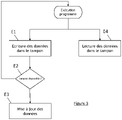
- the first access mode comprises the implementation of a write buffer wear reduction mechanism described in relation to the picture 3 .
- a first portion 31 of the non-volatile memory 3 is reserved for the execution of the program as well as for the storage of the programmer's code as well as data (persistent between two restarts) while a second portion 32 of non-volatile memory 3 is allocated to a write buffer (see picture 2 ).
- a small portion of volatile memory is reserved for the write buffer. The rest is used to store code as well as data.
- step E1 when data must be written (created or updated), the latter are written (step E1) one after the other in the write buffer.
- step E2 of the buffer is checked after each write in the buffer so that it can contain new data.
- the data is written in the buffer at the level of “empty” bytes, which avoids having to go through erase/write cycles, and therefore does not cause wear.
- step E3 the data is updated in the first portion 31 of the memory 3 not volatile (the portion allocated to program execution).
- This update (step E3) is executed page by page. It includes the following steps.
- the content of the page to be updated is copied from the first portion 31 of the non-volatile memory 3 into the content of the volatile memory 4.
- the write buffer 32 is scanned in order to recover the data in their last version (modification or creation). These changes are consolidated to the copied content in volatile memory.
- the content of the volatile memory is copied into the page of the first portion of the non-volatile memory (after erasing the latter).
- the buffer is reset, its content is erased.
- the erase/write procedure in the non-volatile memory is only carried out in cases where the buffer is full or at the capacity limit.
- step E4 when data must be read (step E4), while the write buffer mechanism is active, it is necessary to consolidate the data between those which have just been modified and/or created in the buffer of writing 32 with those present in the non-volatile memory 31. To do this, again, the buffer is scanned in order to check whether the data read is in the write buffer or in the first portion of the non-volatile memory only.
- Deactivation of the wear reduction mechanism can be a stop or a pause of this mechanism.
- the wear reduction mechanism uses a buffer (such as the write buffer 32)
- the shutdown consists of completely emptying the write buffer 32 by updating all the modified pages in the nonvolatile memory 31. Therefore, frequent stops of the write buffer mechanism affect performance by causing writes, and induce non-volatile memory wear.
- pausing the write-buffered mechanism only disables the process of reading data with consolidation.
- the contents of the write buffer are maintained, and negative effects on performance are avoided.
- the wear reduction mechanism of the non-volatile memory implements a counter. If the memory management mechanism is stopped, the counter is set to zero, while if the counter is paused, it is simply interrupted. Again, pausing has less effect on performance than stopping.
- the active or inactive character of the wear reduction mechanism depends solely on the part of the program being executed, that is to say on the location of the execution pointer of the processor 2 during of the execution of the program by this processor 2. It is the programmer of the program who determines in advance, during the coding of the program, whether such and such code instructions of the program must benefit from the wear reduction mechanism or nope.
- the program executed by the electronic device 1 is obtained by a method comprising the following steps, on the basis of a source code.
- the source code includes a plurality of source code instructions written in a predetermined programming language.
- a programmer identifies in the source code a block of source code instructions comprising one or more instructions (step E10).
- the block of source code instructions thus begins with an initial instruction and ends with a final instruction.
- the programmer identifies the block of source code instructions during step E10 using certain specific criteria which will be discussed later.
- the programmer inserts in the source code a deactivation function at the beginning of the block of source code instructions (step E12). In other words, the programmer makes sure that the disable function can be executed just before the initial statement of the block.
- the disable function is configured to disable the previously described non-volatile memory wear reduction mechanism. This deactivation is either a pause or a stop as described above.
- the programmer inserts at the beginning of the identified source code instruction block a call to the disable function.
- the deactivation function is part of the source code, or else is part of a library, for example precompiled. This makes it possible to be able to factorize the source code and simply reuse the deactivation function in several places of the source code.
- the disable function instructions are written directly just before the block.
- the programmer moreover inserts in the source code a reactivation function at the end of the block of source code instructions (step E14). That is, the programmer arranges for the wake-up function to be executed right after the block's final code statement.
- the reactivation function is configured to reactivate the wear reduction mechanism of the nonvolatile memory.
- the programmer inserts a call to the wake-up function at the end of the source code instruction block.
- the deactivation function is part of the source code, or else is part of a library, for example precompiled. This makes it possible to be able to factorize the source code and simply reuse the reactivation function in several places of the source code.
- the instructions of the reactivation function are written directly just before the block.
- identification E10 and insertion E12, 14 are repeated for example for several blocks of source code instructions different from the source code.
- the programmer has the possibility of making a choice between the two modes of deactivation of the mechanism of reduction of wear described previously (stop or pause).
- a generic Disable_WL() function can take as a parameter a value making it possible to select one or the other of these modes for disabling the nonvolatile memory wear reduction mechanism.
- the program has at its disposal not two generic functions but four functions.
- the programmer can surround a block with a Pause_WL() pause function and a Resume_WL() pause output function.
- the programmer can surround such a block with a stop function Stop_WL() and a restart function Start_WL().
- the program intended to be executed by the electronic device 1 is generated from the source code enriched with the calls to the deactivation/reactivation functions (step E16).
- the generation step E16 can for example comprise a compilation of the source code. Such a compilation converts source code instructions into target code instructions, interpretable by the processor 2 of the electronic device 1.
- the invention proposes to determine from the program design stage the sections of code which will benefit from the wear reduction mechanism, and the sections of code where it is acceptable to afford to temporarily deactivate this mechanism in order to save resources. material. It is in this way that it is possible to find an ideal compromise between reduction of wear and saving of material resources.
- the pause function has the advantage of being fast to execute since it does not induce any emptying of a buffer.
- the programmer will therefore place these two functions around a block of instructions adapted to respect this basic condition. If this basic condition is not verified, program execution may be unstable.
- Another criterion for identifying a source code instruction block that the programmer can use is the potential execution frequency of the corresponding target code instruction block after compilation, by the electronic device.
- the programmer can use profiling tools known to those skilled in the art.
- Yet another useful source code instruction block identification criterion is the number of read accesses that will occur in the nonvolatile memory, during an execution of the target code instruction block corresponding to the block. of source code instructions by the electronic device.
- the stop function has the advantage for the programmer of being insertable anywhere in the source code. Since the disable function flushes the buffer, there is no need to ensure that the statement block following a call to the stop function refrains from modifying the contents of this buffer. In other words, the programmer can freely surround any block of source code instructions with the stop and restart functions, without the subsequent risk of instability. On the other hand, the execution of the stop function takes longer than the execution of the pause function, since the buffer must be emptied.
- stop and restart functions is particularly advantageous for surrounding a block that ultimately writes such an amount of data that is greater than or equal to the buffer size. Indeed, in such a case where the buffer is saturated, the wear reduction mechanism using this buffer becomes less effective; the consumption of additional material resources induced by the use of this mechanism then becomes an unprofitable investment. You might as well temporarily deactivate this mechanism to also save hardware resources.
Landscapes
- Engineering & Computer Science (AREA)
- Theoretical Computer Science (AREA)
- General Engineering & Computer Science (AREA)
- Physics & Mathematics (AREA)
- General Physics & Mathematics (AREA)
- Human Computer Interaction (AREA)
- Software Systems (AREA)
- Techniques For Improving Reliability Of Storages (AREA)
Claims (6)
- Verfahren zum Erhalten eines Programms, das dazu bestimmt ist, von einer elektronischen Vorrichtung (1), wie einer Chipkarte, ausgeführt zu werden, umfassend einen nichtflüchtigen Speicher, wobei das Verfahren die Schritte umfasst zum- Einfügen (E12), in einen Quellcode, einer ersten Funktion am Anfang eines Blocks von Quellcodeanweisungen, und Einfügen (E14) einer zweiten Funktion am Ende des Blocks von Quellcodeanweisungen,- nach den Einfügungen, Generieren (E16) des ausführbaren Programms ausgehend von dem Quellcode,wobei- die erste Funktion konfiguriert ist, um einen Mechanismus zur Verringerung des Verschleißes des nichtflüchtigen Speichers zu deaktivieren, wenn das Programm durch die elektronische Vorrichtung ausgeführt wird,- die zweite Funktion konfiguriert ist, um den Mechanismus zur Verringerung des Verschleißes des nichtflüchtigen Speichers zu reaktivieren, wenn das Programm durch die elektronische Vorrichtung ausgeführt wird.
- Verfahren nach dem vorstehenden Anspruch, wobei das Programm einen Block von Zielcodeanweisungen umfasst, der ausgehend von dem Block von Quellcodeanweisungen generiert wird, und wobei der Block von Quellcodeanweisungen in Abhängigkeit von einer potenziellen Ausführungsfrequenz des Blocks von Zielcodeanweisungen während der Ausführung des Programms durch die elektronische Vorrichtung bestimmt wird.
- Verfahren nach einem der vorstehenden Ansprüche, wobei das Programm einen Block von Zielcodeanweisungen umfasst, der ausgehend von dem Block von Quellcodeanweisungen generiert wird, und wobei der Block von Quellcodeanweisungen in Abhängigkeit von einer Anzahl von Lesezugriffen auf den nichtflüchtigen Speicher während einer Ausführung des Blocks von Zielcodeanweisungen durch die elektronische Vorrichtung bestimmt wird.
- Verfahren nach einem der vorstehenden Ansprüche, wobei das Programm einen Block von Zielcodeanweisungen umfasst, der ausgehend von dem Block von Quellcodeanweisungen generiert wird, und wobei der Block von Quellcodeanweisungen in Abhängigkeit von einer Menge von Daten bestimmt wird, die während einer Ausführung des Blocks von Zielcodeanweisungen wahrscheinlich durch die elektronische Vorrichtung in den nichtflüchtigen Speicher geschrieben werden.
- Computerprogrammprodukt, das Anweisungen umfasst, die, wenn das Programm von einem Computer ausgeführt wird, diesen dazu veranlassen, das Verfahren nach einem der vorstehenden Ansprüche zu implementieren.
- Elektronische Vorrichtung (1), wie eine Chipkarte, umfassend einen nichtflüchtigen Speicher (3), einen Mechanismus zur Verringerung des Verschleißes des nichtflüchtigen Speichers und mindestens einen Prozessor (4), konfiguriert, um das Computerprogrammprodukt nach dem vorstehenden Anspruch auszuführen.
Applications Claiming Priority (1)
| Application Number | Priority Date | Filing Date | Title |
|---|---|---|---|
| FR1761223A FR3074317B1 (fr) | 2017-11-27 | 2017-11-27 | Procede d'acces a une zone memoire non volatile de type flash d'un element securise, tel qu'une carte a puce |
Publications (2)
| Publication Number | Publication Date |
|---|---|
| EP3489833A1 EP3489833A1 (de) | 2019-05-29 |
| EP3489833B1 true EP3489833B1 (de) | 2022-05-25 |
Family
ID=61802038
Family Applications (1)
| Application Number | Title | Priority Date | Filing Date |
|---|---|---|---|
| EP18306569.7A Active EP3489833B1 (de) | 2017-11-27 | 2018-11-26 | Verfahren zur erstellung eines programms, das für die ausführung durch eine elektronische vorrichtung bestimmt ist, wie beispielsweise eine chip-karte, die einen nicht-flüchtigen speicher umfasst |
Country Status (3)
| Country | Link |
|---|---|
| US (1) | US10776092B2 (de) |
| EP (1) | EP3489833B1 (de) |
| FR (1) | FR3074317B1 (de) |
Families Citing this family (1)
| Publication number | Priority date | Publication date | Assignee | Title |
|---|---|---|---|---|
| CN118210509A (zh) * | 2022-12-16 | 2024-06-18 | 澜起科技股份有限公司 | 执行代码的方法、数据处理装置及系统 |
Citations (1)
| Publication number | Priority date | Publication date | Assignee | Title |
|---|---|---|---|---|
| US20140379971A1 (en) * | 2012-03-15 | 2014-12-25 | Kabushiki Kaisha Toshiba | Video distribution server and ssd control method |
Family Cites Families (18)
| Publication number | Priority date | Publication date | Assignee | Title |
|---|---|---|---|---|
| CA2267477C (en) * | 1999-03-30 | 2003-10-14 | Object Technology International Inc. | Packaging memory image files |
| US7970983B2 (en) * | 2007-10-14 | 2011-06-28 | Sandisk Il Ltd. | Identity-based flash management |
| KR101464338B1 (ko) * | 2007-10-25 | 2014-11-25 | 삼성전자주식회사 | 불휘발성 메모리 장치를 이용한 데이터 저장장치, 메모리시스템, 그리고 컴퓨터 시스템 |
| US7917689B2 (en) * | 2007-12-28 | 2011-03-29 | Intel Corporation | Methods and apparatuses for nonvolatile memory wear leveling |
| JP4745356B2 (ja) * | 2008-03-01 | 2011-08-10 | 株式会社東芝 | メモリシステム |
| US8001318B1 (en) * | 2008-10-28 | 2011-08-16 | Netapp, Inc. | Wear leveling for low-wear areas of low-latency random read memory |
| US8495281B2 (en) * | 2009-12-04 | 2013-07-23 | International Business Machines Corporation | Intra-block memory wear leveling |
| US8521948B2 (en) * | 2011-01-03 | 2013-08-27 | Apple Inc. | Handling dynamic and static data for a system having non-volatile memory |
| KR102003930B1 (ko) * | 2012-07-31 | 2019-07-25 | 삼성전자주식회사 | 불휘발성 메모리 장치의 데이터 라이팅 제어방법 및 웨어레벨링 제어 기능을 가지는 메모리 콘트롤러 |
| JP2015204073A (ja) * | 2014-04-16 | 2015-11-16 | キヤノン株式会社 | 情報処理装置、情報処理端末、情報処理方法およびプログラム |
| WO2015162758A1 (ja) * | 2014-04-24 | 2015-10-29 | 株式会社日立製作所 | ストレージシステム |
| US20160210044A1 (en) * | 2015-01-15 | 2016-07-21 | Commvault Systems, Inc. | Intelligent hybrid drive caching |
| KR102507743B1 (ko) * | 2016-02-04 | 2023-03-09 | 삼성전자주식회사 | 메모리 관리 방법 및 그 전자 장치 |
| KR102438988B1 (ko) * | 2016-04-07 | 2022-09-02 | 삼성전자주식회사 | 랜덤화 연산을 수행하는 불휘발성 메모리 장치 |
| US10528462B2 (en) * | 2016-09-26 | 2020-01-07 | Intel Corporation | Storage device having improved write uniformity stability |
| US10542089B2 (en) * | 2017-03-10 | 2020-01-21 | Toshiba Memory Corporation | Large scale implementation of a plurality of open channel solid state drives |
| US20180349287A1 (en) * | 2017-06-02 | 2018-12-06 | Dell Products L.P. | Persistent Storage Device Information Cache |
| US10388351B2 (en) * | 2017-08-30 | 2019-08-20 | Micron Technology, Inc. | Wear leveling for random access and ferroelectric memory |
-
2017
- 2017-11-27 FR FR1761223A patent/FR3074317B1/fr active Active
-
2018
- 2018-11-26 US US16/200,457 patent/US10776092B2/en active Active
- 2018-11-26 EP EP18306569.7A patent/EP3489833B1/de active Active
Patent Citations (1)
| Publication number | Priority date | Publication date | Assignee | Title |
|---|---|---|---|---|
| US20140379971A1 (en) * | 2012-03-15 | 2014-12-25 | Kabushiki Kaisha Toshiba | Video distribution server and ssd control method |
Also Published As
| Publication number | Publication date |
|---|---|
| US20190163454A1 (en) | 2019-05-30 |
| EP3489833A1 (de) | 2019-05-29 |
| FR3074317A1 (fr) | 2019-05-31 |
| FR3074317B1 (fr) | 2019-11-22 |
| US10776092B2 (en) | 2020-09-15 |
Similar Documents
| Publication | Publication Date | Title |
|---|---|---|
| CN111796856B (zh) | 差分升级方法及装置、存储介质、计算机设备 | |
| US8463826B2 (en) | Incremental garbage collection for non-volatile memories | |
| KR100584338B1 (ko) | 소프트웨어 업데이트 방법 및 시스템 | |
| US20100174853A1 (en) | User device including flash and random write cache and method writing data | |
| US20130219106A1 (en) | Trim token journaling | |
| KR101583002B1 (ko) | 컴퓨팅 시스템, 그것의 부팅 방법, 및 코드 데이터 피닝 방법 | |
| KR102127284B1 (ko) | 불휘발성 메모리 장치 및 그것의 관리 방법 | |
| EP2310941A1 (de) | Verfahren und einrichtung zum aktualisieren einer computeranwendung | |
| US20140304497A1 (en) | Electronic device having function of booting operating system by bootloader, method of performing the same function, and storage medium | |
| US20090037648A1 (en) | Input/output control method and apparatus optimized for flash memory | |
| CN112162773B (zh) | 差分升级方法及装置、存储介质、终端 | |
| US20170269870A1 (en) | Memory controller, nonvolatile storage device, nonvolatile storage system, and memory control method | |
| CN106775490A (zh) | 一种基于非易失内存的内核日志存储方法及装置 | |
| EP3489833B1 (de) | Verfahren zur erstellung eines programms, das für die ausführung durch eine elektronische vorrichtung bestimmt ist, wie beispielsweise eine chip-karte, die einen nicht-flüchtigen speicher umfasst | |
| CN104951376A (zh) | 参数优化方法及参数优化装置 | |
| US20160321057A1 (en) | Electronic apparatus | |
| CN111176686B (zh) | 一种bios升级方法、系统、电子设备及存储介质 | |
| WO2012107189A2 (fr) | Procede de reprogrammation d'un calculateur, support de memorisation de donnees et calculateur de vehicule automobile | |
| US20130093778A1 (en) | Display apparatus and method for controlling the same | |
| CN101908009B (zh) | 文件备份与使用方法 | |
| EP3392791B1 (de) | Verfahren zur ausführung eines programms, das zur interpretation durch eine virtuelle maschine bestimmt ist, die gegen angriffe durch fehler-injektion geschützt ist | |
| CN111813708B (zh) | 用于存储装置的块映射系统和方法 | |
| US20070198788A1 (en) | Memory access methods | |
| EP4312128A1 (de) | Verfahren zur verwaltung eines speichers eines sicheren elements | |
| CN103559140A (zh) | 一种用于flash存储数据的方法及装置 |
Legal Events
| Date | Code | Title | Description |
|---|---|---|---|
| PUAI | Public reference made under article 153(3) epc to a published international application that has entered the european phase |
Free format text: ORIGINAL CODE: 0009012 |
|
| STAA | Information on the status of an ep patent application or granted ep patent |
Free format text: STATUS: THE APPLICATION HAS BEEN PUBLISHED |
|
| AK | Designated contracting states |
Kind code of ref document: A1 Designated state(s): AL AT BE BG CH CY CZ DE DK EE ES FI FR GB GR HR HU IE IS IT LI LT LU LV MC MK MT NL NO PL PT RO RS SE SI SK SM TR |
|
| AX | Request for extension of the european patent |
Extension state: BA ME |
|
| STAA | Information on the status of an ep patent application or granted ep patent |
Free format text: STATUS: REQUEST FOR EXAMINATION WAS MADE |
|
| 17P | Request for examination filed |
Effective date: 20190731 |
|
| RBV | Designated contracting states (corrected) |
Designated state(s): AL AT BE BG CH CY CZ DE DK EE ES FI FR GB GR HR HU IE IS IT LI LT LU LV MC MK MT NL NO PL PT RO RS SE SI SK SM TR |
|
| STAA | Information on the status of an ep patent application or granted ep patent |
Free format text: STATUS: EXAMINATION IS IN PROGRESS |
|
| 17Q | First examination report despatched |
Effective date: 20201013 |
|
| RIC1 | Information provided on ipc code assigned before grant |
Ipc: G06F 8/70 20180101ALN20211223BHEP Ipc: G06F 3/06 20060101ALI20211223BHEP Ipc: G06F 12/02 20060101AFI20211223BHEP |
|
| GRAP | Despatch of communication of intention to grant a patent |
Free format text: ORIGINAL CODE: EPIDOSNIGR1 |
|
| STAA | Information on the status of an ep patent application or granted ep patent |
Free format text: STATUS: GRANT OF PATENT IS INTENDED |
|
| INTG | Intention to grant announced |
Effective date: 20220201 |
|
| GRAS | Grant fee paid |
Free format text: ORIGINAL CODE: EPIDOSNIGR3 |
|
| GRAA | (expected) grant |
Free format text: ORIGINAL CODE: 0009210 |
|
| STAA | Information on the status of an ep patent application or granted ep patent |
Free format text: STATUS: THE PATENT HAS BEEN GRANTED |
|
| AK | Designated contracting states |
Kind code of ref document: B1 Designated state(s): AL AT BE BG CH CY CZ DE DK EE ES FI FR GB GR HR HU IE IS IT LI LT LU LV MC MK MT NL NO PL PT RO RS SE SI SK SM TR |
|
| REG | Reference to a national code |
Ref country code: GB Ref legal event code: FG4D Free format text: NOT ENGLISH |
|
| REG | Reference to a national code |
Ref country code: CH Ref legal event code: EP |
|
| REG | Reference to a national code |
Ref country code: AT Ref legal event code: REF Ref document number: 1494543 Country of ref document: AT Kind code of ref document: T Effective date: 20220615 Ref country code: DE Ref legal event code: R096 Ref document number: 602018035953 Country of ref document: DE |
|
| REG | Reference to a national code |
Ref country code: IE Ref legal event code: FG4D Free format text: LANGUAGE OF EP DOCUMENT: FRENCH |
|
| REG | Reference to a national code |
Ref country code: LT Ref legal event code: MG9D |
|
| REG | Reference to a national code |
Ref country code: NL Ref legal event code: MP Effective date: 20220525 |
|
| REG | Reference to a national code |
Ref country code: AT Ref legal event code: MK05 Ref document number: 1494543 Country of ref document: AT Kind code of ref document: T Effective date: 20220525 |
|
| PG25 | Lapsed in a contracting state [announced via postgrant information from national office to epo] |
Ref country code: SE Free format text: LAPSE BECAUSE OF FAILURE TO SUBMIT A TRANSLATION OF THE DESCRIPTION OR TO PAY THE FEE WITHIN THE PRESCRIBED TIME-LIMIT Effective date: 20220525 Ref country code: PT Free format text: LAPSE BECAUSE OF FAILURE TO SUBMIT A TRANSLATION OF THE DESCRIPTION OR TO PAY THE FEE WITHIN THE PRESCRIBED TIME-LIMIT Effective date: 20220926 Ref country code: NO Free format text: LAPSE BECAUSE OF FAILURE TO SUBMIT A TRANSLATION OF THE DESCRIPTION OR TO PAY THE FEE WITHIN THE PRESCRIBED TIME-LIMIT Effective date: 20220825 Ref country code: NL Free format text: LAPSE BECAUSE OF FAILURE TO SUBMIT A TRANSLATION OF THE DESCRIPTION OR TO PAY THE FEE WITHIN THE PRESCRIBED TIME-LIMIT Effective date: 20220525 Ref country code: LT Free format text: LAPSE BECAUSE OF FAILURE TO SUBMIT A TRANSLATION OF THE DESCRIPTION OR TO PAY THE FEE WITHIN THE PRESCRIBED TIME-LIMIT Effective date: 20220525 Ref country code: HR Free format text: LAPSE BECAUSE OF FAILURE TO SUBMIT A TRANSLATION OF THE DESCRIPTION OR TO PAY THE FEE WITHIN THE PRESCRIBED TIME-LIMIT Effective date: 20220525 Ref country code: GR Free format text: LAPSE BECAUSE OF FAILURE TO SUBMIT A TRANSLATION OF THE DESCRIPTION OR TO PAY THE FEE WITHIN THE PRESCRIBED TIME-LIMIT Effective date: 20220826 Ref country code: FI Free format text: LAPSE BECAUSE OF FAILURE TO SUBMIT A TRANSLATION OF THE DESCRIPTION OR TO PAY THE FEE WITHIN THE PRESCRIBED TIME-LIMIT Effective date: 20220525 Ref country code: ES Free format text: LAPSE BECAUSE OF FAILURE TO SUBMIT A TRANSLATION OF THE DESCRIPTION OR TO PAY THE FEE WITHIN THE PRESCRIBED TIME-LIMIT Effective date: 20220525 Ref country code: BG Free format text: LAPSE BECAUSE OF FAILURE TO SUBMIT A TRANSLATION OF THE DESCRIPTION OR TO PAY THE FEE WITHIN THE PRESCRIBED TIME-LIMIT Effective date: 20220825 Ref country code: AT Free format text: LAPSE BECAUSE OF FAILURE TO SUBMIT A TRANSLATION OF THE DESCRIPTION OR TO PAY THE FEE WITHIN THE PRESCRIBED TIME-LIMIT Effective date: 20220525 |
|
| PG25 | Lapsed in a contracting state [announced via postgrant information from national office to epo] |
Ref country code: RS Free format text: LAPSE BECAUSE OF FAILURE TO SUBMIT A TRANSLATION OF THE DESCRIPTION OR TO PAY THE FEE WITHIN THE PRESCRIBED TIME-LIMIT Effective date: 20220525 Ref country code: PL Free format text: LAPSE BECAUSE OF FAILURE TO SUBMIT A TRANSLATION OF THE DESCRIPTION OR TO PAY THE FEE WITHIN THE PRESCRIBED TIME-LIMIT Effective date: 20220525 Ref country code: LV Free format text: LAPSE BECAUSE OF FAILURE TO SUBMIT A TRANSLATION OF THE DESCRIPTION OR TO PAY THE FEE WITHIN THE PRESCRIBED TIME-LIMIT Effective date: 20220525 Ref country code: IS Free format text: LAPSE BECAUSE OF FAILURE TO SUBMIT A TRANSLATION OF THE DESCRIPTION OR TO PAY THE FEE WITHIN THE PRESCRIBED TIME-LIMIT Effective date: 20220925 |
|
| PG25 | Lapsed in a contracting state [announced via postgrant information from national office to epo] |
Ref country code: SM Free format text: LAPSE BECAUSE OF FAILURE TO SUBMIT A TRANSLATION OF THE DESCRIPTION OR TO PAY THE FEE WITHIN THE PRESCRIBED TIME-LIMIT Effective date: 20220525 Ref country code: SK Free format text: LAPSE BECAUSE OF FAILURE TO SUBMIT A TRANSLATION OF THE DESCRIPTION OR TO PAY THE FEE WITHIN THE PRESCRIBED TIME-LIMIT Effective date: 20220525 Ref country code: RO Free format text: LAPSE BECAUSE OF FAILURE TO SUBMIT A TRANSLATION OF THE DESCRIPTION OR TO PAY THE FEE WITHIN THE PRESCRIBED TIME-LIMIT Effective date: 20220525 Ref country code: EE Free format text: LAPSE BECAUSE OF FAILURE TO SUBMIT A TRANSLATION OF THE DESCRIPTION OR TO PAY THE FEE WITHIN THE PRESCRIBED TIME-LIMIT Effective date: 20220525 Ref country code: DK Free format text: LAPSE BECAUSE OF FAILURE TO SUBMIT A TRANSLATION OF THE DESCRIPTION OR TO PAY THE FEE WITHIN THE PRESCRIBED TIME-LIMIT Effective date: 20220525 Ref country code: CZ Free format text: LAPSE BECAUSE OF FAILURE TO SUBMIT A TRANSLATION OF THE DESCRIPTION OR TO PAY THE FEE WITHIN THE PRESCRIBED TIME-LIMIT Effective date: 20220525 |
|
| REG | Reference to a national code |
Ref country code: DE Ref legal event code: R097 Ref document number: 602018035953 Country of ref document: DE |
|
| PG25 | Lapsed in a contracting state [announced via postgrant information from national office to epo] |
Ref country code: AL Free format text: LAPSE BECAUSE OF FAILURE TO SUBMIT A TRANSLATION OF THE DESCRIPTION OR TO PAY THE FEE WITHIN THE PRESCRIBED TIME-LIMIT Effective date: 20220525 |
|
| PLBE | No opposition filed within time limit |
Free format text: ORIGINAL CODE: 0009261 |
|
| STAA | Information on the status of an ep patent application or granted ep patent |
Free format text: STATUS: NO OPPOSITION FILED WITHIN TIME LIMIT |
|
| 26N | No opposition filed |
Effective date: 20230228 |
|
| PG25 | Lapsed in a contracting state [announced via postgrant information from national office to epo] |
Ref country code: SI Free format text: LAPSE BECAUSE OF FAILURE TO SUBMIT A TRANSLATION OF THE DESCRIPTION OR TO PAY THE FEE WITHIN THE PRESCRIBED TIME-LIMIT Effective date: 20220525 |
|
| P01 | Opt-out of the competence of the unified patent court (upc) registered |
Effective date: 20230428 |
|
| PG25 | Lapsed in a contracting state [announced via postgrant information from national office to epo] |
Ref country code: MC Free format text: LAPSE BECAUSE OF FAILURE TO SUBMIT A TRANSLATION OF THE DESCRIPTION OR TO PAY THE FEE WITHIN THE PRESCRIBED TIME-LIMIT Effective date: 20220525 |
|
| REG | Reference to a national code |
Ref country code: CH Ref legal event code: PL |
|
| GBPC | Gb: european patent ceased through non-payment of renewal fee |
Effective date: 20221126 |
|
| REG | Reference to a national code |
Ref country code: BE Ref legal event code: MM Effective date: 20221130 |
|
| PG25 | Lapsed in a contracting state [announced via postgrant information from national office to epo] |
Ref country code: LI Free format text: LAPSE BECAUSE OF NON-PAYMENT OF DUE FEES Effective date: 20221130 Ref country code: CH Free format text: LAPSE BECAUSE OF NON-PAYMENT OF DUE FEES Effective date: 20221130 |
|
| PG25 | Lapsed in a contracting state [announced via postgrant information from national office to epo] |
Ref country code: LU Free format text: LAPSE BECAUSE OF NON-PAYMENT OF DUE FEES Effective date: 20221126 |
|
| PG25 | Lapsed in a contracting state [announced via postgrant information from national office to epo] |
Ref country code: IE Free format text: LAPSE BECAUSE OF NON-PAYMENT OF DUE FEES Effective date: 20221126 Ref country code: GB Free format text: LAPSE BECAUSE OF NON-PAYMENT OF DUE FEES Effective date: 20221126 |
|
| PG25 | Lapsed in a contracting state [announced via postgrant information from national office to epo] |
Ref country code: BE Free format text: LAPSE BECAUSE OF NON-PAYMENT OF DUE FEES Effective date: 20221130 |
|
| PG25 | Lapsed in a contracting state [announced via postgrant information from national office to epo] |
Ref country code: IT Free format text: LAPSE BECAUSE OF FAILURE TO SUBMIT A TRANSLATION OF THE DESCRIPTION OR TO PAY THE FEE WITHIN THE PRESCRIBED TIME-LIMIT Effective date: 20220525 |
|
| PG25 | Lapsed in a contracting state [announced via postgrant information from national office to epo] |
Ref country code: HU Free format text: LAPSE BECAUSE OF FAILURE TO SUBMIT A TRANSLATION OF THE DESCRIPTION OR TO PAY THE FEE WITHIN THE PRESCRIBED TIME-LIMIT; INVALID AB INITIO Effective date: 20181126 |
|
| PG25 | Lapsed in a contracting state [announced via postgrant information from national office to epo] |
Ref country code: CY Free format text: LAPSE BECAUSE OF FAILURE TO SUBMIT A TRANSLATION OF THE DESCRIPTION OR TO PAY THE FEE WITHIN THE PRESCRIBED TIME-LIMIT Effective date: 20220525 |
|
| PG25 | Lapsed in a contracting state [announced via postgrant information from national office to epo] |
Ref country code: MK Free format text: LAPSE BECAUSE OF FAILURE TO SUBMIT A TRANSLATION OF THE DESCRIPTION OR TO PAY THE FEE WITHIN THE PRESCRIBED TIME-LIMIT Effective date: 20220525 |
|
| PG25 | Lapsed in a contracting state [announced via postgrant information from national office to epo] |
Ref country code: TR Free format text: LAPSE BECAUSE OF FAILURE TO SUBMIT A TRANSLATION OF THE DESCRIPTION OR TO PAY THE FEE WITHIN THE PRESCRIBED TIME-LIMIT Effective date: 20220525 |
|
| PG25 | Lapsed in a contracting state [announced via postgrant information from national office to epo] |
Ref country code: MT Free format text: LAPSE BECAUSE OF FAILURE TO SUBMIT A TRANSLATION OF THE DESCRIPTION OR TO PAY THE FEE WITHIN THE PRESCRIBED TIME-LIMIT Effective date: 20220525 |
|
| PG25 | Lapsed in a contracting state [announced via postgrant information from national office to epo] |
Ref country code: BG Free format text: LAPSE BECAUSE OF FAILURE TO SUBMIT A TRANSLATION OF THE DESCRIPTION OR TO PAY THE FEE WITHIN THE PRESCRIBED TIME-LIMIT Effective date: 20220525 |
|
| PG25 | Lapsed in a contracting state [announced via postgrant information from national office to epo] |
Ref country code: BG Free format text: LAPSE BECAUSE OF FAILURE TO SUBMIT A TRANSLATION OF THE DESCRIPTION OR TO PAY THE FEE WITHIN THE PRESCRIBED TIME-LIMIT Effective date: 20220525 |
|
| REG | Reference to a national code |
Ref country code: DE Ref legal event code: R081 Ref document number: 602018035953 Country of ref document: DE Owner name: IDEMIA FRANCE, FR Free format text: FORMER OWNER: IDEMIA IDENTITY & SECURITY FRANCE, COURBEVOIE, FR |
|
| PGFP | Annual fee paid to national office [announced via postgrant information from national office to epo] |
Ref country code: DE Payment date: 20251022 Year of fee payment: 8 |
|
| PGFP | Annual fee paid to national office [announced via postgrant information from national office to epo] |
Ref country code: FR Payment date: 20251022 Year of fee payment: 8 |