EP3487059B1 - Bereitstellung von positionsinformationen und steigerung der stromqualität von parallel geschalteten wechselrichtern - Google Patents
Bereitstellung von positionsinformationen und steigerung der stromqualität von parallel geschalteten wechselrichtern Download PDFInfo
- Publication number
- EP3487059B1 EP3487059B1 EP18207048.2A EP18207048A EP3487059B1 EP 3487059 B1 EP3487059 B1 EP 3487059B1 EP 18207048 A EP18207048 A EP 18207048A EP 3487059 B1 EP3487059 B1 EP 3487059B1
- Authority
- EP
- European Patent Office
- Prior art keywords
- phase
- power
- power device
- inverter
- output terminal
- Prior art date
- Legal status (The legal status is an assumption and is not a legal conclusion. Google has not performed a legal analysis and makes no representation as to the accuracy of the status listed.)
- Active
Links
Images








Classifications
-
- H—ELECTRICITY
- H02—GENERATION; CONVERSION OR DISTRIBUTION OF ELECTRIC POWER
- H02J—ELECTRIC POWER NETWORKS; CIRCUIT ARRANGEMENTS OR SYSTEMS FOR SUPPLYING OR DISTRIBUTING ELECTRIC POWER; SYSTEMS FOR STORING ELECTRIC ENERGY
- H02J13/00—Circuit arrangements for providing remote monitoring or remote control of equipment in a power distribution network
- H02J13/13—Circuit arrangements for providing remote monitoring or remote control of equipment in a power distribution network characterised by the transmission of data to equipment in the power network
- H02J13/1321—Circuit arrangements for providing remote monitoring or remote control of equipment in a power distribution network characterised by the transmission of data to equipment in the power network using a wired telecommunication network or a data transmission bus
- H02J13/1323—Circuit arrangements for providing remote monitoring or remote control of equipment in a power distribution network characterised by the transmission of data to equipment in the power network using a wired telecommunication network or a data transmission bus using optical fibres
-
- H—ELECTRICITY
- H02—GENERATION; CONVERSION OR DISTRIBUTION OF ELECTRIC POWER
- H02J—ELECTRIC POWER NETWORKS; CIRCUIT ARRANGEMENTS OR SYSTEMS FOR SUPPLYING OR DISTRIBUTING ELECTRIC POWER; SYSTEMS FOR STORING ELECTRIC ENERGY
- H02J13/00—Circuit arrangements for providing remote monitoring or remote control of equipment in a power distribution network
- H02J13/12—Monitoring network conditions, e.g. electrical magnitudes or operational status
-
- H—ELECTRICITY
- H02—GENERATION; CONVERSION OR DISTRIBUTION OF ELECTRIC POWER
- H02J—ELECTRIC POWER NETWORKS; CIRCUIT ARRANGEMENTS OR SYSTEMS FOR SUPPLYING OR DISTRIBUTING ELECTRIC POWER; SYSTEMS FOR STORING ELECTRIC ENERGY
- H02J3/00—Circuit arrangements for AC mains or AC distribution networks
- H02J3/38—Arrangements for feeding a single network from two or more generators or sources in parallel; Arrangements for feeding already energised networks from additional generators or sources in parallel
-
- H—ELECTRICITY
- H02—GENERATION; CONVERSION OR DISTRIBUTION OF ELECTRIC POWER
- H02J—ELECTRIC POWER NETWORKS; CIRCUIT ARRANGEMENTS OR SYSTEMS FOR SUPPLYING OR DISTRIBUTING ELECTRIC POWER; SYSTEMS FOR STORING ELECTRIC ENERGY
- H02J3/00—Circuit arrangements for AC mains or AC distribution networks
- H02J3/38—Arrangements for feeding a single network from two or more generators or sources in parallel; Arrangements for feeding already energised networks from additional generators or sources in parallel
- H02J3/46—Controlling the sharing of generated power between the generators, sources or networks
- H02J3/48—Controlling the sharing of active power
-
- H—ELECTRICITY
- H02—GENERATION; CONVERSION OR DISTRIBUTION OF ELECTRIC POWER
- H02M—APPARATUS FOR CONVERSION BETWEEN AC AND AC, BETWEEN AC AND DC, OR BETWEEN DC AND DC, AND FOR USE WITH MAINS OR SIMILAR POWER SUPPLY SYSTEMS; CONVERSION OF DC OR AC INPUT POWER INTO SURGE OUTPUT POWER; CONTROL OR REGULATION THEREOF
- H02M7/00—Conversion of AC power input into DC power output; Conversion of DC power input into AC power output
- H02M7/003—Constructional details, e.g. physical layout, assembly, wiring or busbar connections
-
- H—ELECTRICITY
- H02—GENERATION; CONVERSION OR DISTRIBUTION OF ELECTRIC POWER
- H02M—APPARATUS FOR CONVERSION BETWEEN AC AND AC, BETWEEN AC AND DC, OR BETWEEN DC AND DC, AND FOR USE WITH MAINS OR SIMILAR POWER SUPPLY SYSTEMS; CONVERSION OF DC OR AC INPUT POWER INTO SURGE OUTPUT POWER; CONTROL OR REGULATION THEREOF
- H02M7/00—Conversion of AC power input into DC power output; Conversion of DC power input into AC power output
- H02M7/42—Conversion of DC power input into AC power output without possibility of reversal
-
- H—ELECTRICITY
- H02—GENERATION; CONVERSION OR DISTRIBUTION OF ELECTRIC POWER
- H02M—APPARATUS FOR CONVERSION BETWEEN AC AND AC, BETWEEN AC AND DC, OR BETWEEN DC AND DC, AND FOR USE WITH MAINS OR SIMILAR POWER SUPPLY SYSTEMS; CONVERSION OF DC OR AC INPUT POWER INTO SURGE OUTPUT POWER; CONTROL OR REGULATION THEREOF
- H02M7/00—Conversion of AC power input into DC power output; Conversion of DC power input into AC power output
- H02M7/42—Conversion of DC power input into AC power output without possibility of reversal
- H02M7/44—Conversion of DC power input into AC power output without possibility of reversal by static converters
- H02M7/48—Conversion of DC power input into AC power output without possibility of reversal by static converters using discharge tubes with control electrode or semiconductor devices with control electrode
- H02M7/493—Conversion of DC power input into AC power output without possibility of reversal by static converters using discharge tubes with control electrode or semiconductor devices with control electrode the static converters being arranged for operation in parallel
-
- G—PHYSICS
- G01—MEASURING; TESTING
- G01R—MEASURING ELECTRIC VARIABLES; MEASURING MAGNETIC VARIABLES
- G01R29/00—Arrangements for measuring or indicating electric quantities not covered by groups G01R19/00 - G01R27/00
- G01R29/18—Indicating phase sequence; Indicating synchronism
-
- H—ELECTRICITY
- H02—GENERATION; CONVERSION OR DISTRIBUTION OF ELECTRIC POWER
- H02J—ELECTRIC POWER NETWORKS; CIRCUIT ARRANGEMENTS OR SYSTEMS FOR SUPPLYING OR DISTRIBUTING ELECTRIC POWER; SYSTEMS FOR STORING ELECTRIC ENERGY
- H02J1/00—Circuit arrangements for DC mains or DC distribution networks
- H02J1/10—Parallel operation of DC sources
-
- H—ELECTRICITY
- H02—GENERATION; CONVERSION OR DISTRIBUTION OF ELECTRIC POWER
- H02J—ELECTRIC POWER NETWORKS; CIRCUIT ARRANGEMENTS OR SYSTEMS FOR SUPPLYING OR DISTRIBUTING ELECTRIC POWER; SYSTEMS FOR STORING ELECTRIC ENERGY
- H02J2101/00—Supply or distribution of decentralised, dispersed or local electric power generation
- H02J2101/20—Dispersed power generation using renewable energy sources
- H02J2101/22—Solar energy
- H02J2101/24—Photovoltaics
-
- H—ELECTRICITY
- H02—GENERATION; CONVERSION OR DISTRIBUTION OF ELECTRIC POWER
- H02J—ELECTRIC POWER NETWORKS; CIRCUIT ARRANGEMENTS OR SYSTEMS FOR SUPPLYING OR DISTRIBUTING ELECTRIC POWER; SYSTEMS FOR STORING ELECTRIC ENERGY
- H02J3/00—Circuit arrangements for AC mains or AC distribution networks
- H02J3/38—Arrangements for feeding a single network from two or more generators or sources in parallel; Arrangements for feeding already energised networks from additional generators or sources in parallel
- H02J3/381—Dispersed generators
-
- H—ELECTRICITY
- H02—GENERATION; CONVERSION OR DISTRIBUTION OF ELECTRIC POWER
- H02J—ELECTRIC POWER NETWORKS; CIRCUIT ARRANGEMENTS OR SYSTEMS FOR SUPPLYING OR DISTRIBUTING ELECTRIC POWER; SYSTEMS FOR STORING ELECTRIC ENERGY
- H02J3/00—Circuit arrangements for AC mains or AC distribution networks
- H02J3/38—Arrangements for feeding a single network from two or more generators or sources in parallel; Arrangements for feeding already energised networks from additional generators or sources in parallel
- H02J3/388—Arrangements for the handling of islanding, e.g. for disconnection or for avoiding the disconnection of power
-
- H—ELECTRICITY
- H02—GENERATION; CONVERSION OR DISTRIBUTION OF ELECTRIC POWER
- H02J—ELECTRIC POWER NETWORKS; CIRCUIT ARRANGEMENTS OR SYSTEMS FOR SUPPLYING OR DISTRIBUTING ELECTRIC POWER; SYSTEMS FOR STORING ELECTRIC ENERGY
- H02J7/00—Circuit arrangements for charging or discharging batteries or for supplying loads from batteries
- H02J7/34—Parallel operation in networks using both storage and other DC sources, e.g. providing buffering
-
- H—ELECTRICITY
- H02—GENERATION; CONVERSION OR DISTRIBUTION OF ELECTRIC POWER
- H02M—APPARATUS FOR CONVERSION BETWEEN AC AND AC, BETWEEN AC AND DC, OR BETWEEN DC AND DC, AND FOR USE WITH MAINS OR SIMILAR POWER SUPPLY SYSTEMS; CONVERSION OF DC OR AC INPUT POWER INTO SURGE OUTPUT POWER; CONTROL OR REGULATION THEREOF
- H02M3/00—Conversion of DC power input into DC power output
- H02M3/02—Conversion of DC power input into DC power output without intermediate conversion into AC
- H02M3/04—Conversion of DC power input into DC power output without intermediate conversion into AC by static converters
- H02M3/10—Conversion of DC power input into DC power output without intermediate conversion into AC by static converters using discharge tubes with control electrode or semiconductor devices with control electrode
- H02M3/145—Conversion of DC power input into DC power output without intermediate conversion into AC by static converters using discharge tubes with control electrode or semiconductor devices with control electrode using devices of a triode or transistor type requiring continuous application of a control signal
- H02M3/155—Conversion of DC power input into DC power output without intermediate conversion into AC by static converters using discharge tubes with control electrode or semiconductor devices with control electrode using devices of a triode or transistor type requiring continuous application of a control signal using semiconductor devices only
- H02M3/156—Conversion of DC power input into DC power output without intermediate conversion into AC by static converters using discharge tubes with control electrode or semiconductor devices with control electrode using devices of a triode or transistor type requiring continuous application of a control signal using semiconductor devices only with automatic control of output voltage or current, e.g. switching regulators
- H02M3/158—Conversion of DC power input into DC power output without intermediate conversion into AC by static converters using discharge tubes with control electrode or semiconductor devices with control electrode using devices of a triode or transistor type requiring continuous application of a control signal using semiconductor devices only with automatic control of output voltage or current, e.g. switching regulators including plural semiconductor devices as final control devices for a single load
-
- Y—GENERAL TAGGING OF NEW TECHNOLOGICAL DEVELOPMENTS; GENERAL TAGGING OF CROSS-SECTIONAL TECHNOLOGIES SPANNING OVER SEVERAL SECTIONS OF THE IPC; TECHNICAL SUBJECTS COVERED BY FORMER USPC CROSS-REFERENCE ART COLLECTIONS [XRACs] AND DIGESTS
- Y04—INFORMATION OR COMMUNICATION TECHNOLOGIES HAVING AN IMPACT ON OTHER TECHNOLOGY AREAS
- Y04S—SYSTEMS INTEGRATING TECHNOLOGIES RELATED TO POWER NETWORK OPERATION, COMMUNICATION OR INFORMATION TECHNOLOGIES FOR IMPROVING THE ELECTRICAL POWER GENERATION, TRANSMISSION, DISTRIBUTION, MANAGEMENT OR USAGE, i.e. SMART GRIDS
- Y04S10/00—Systems supporting electrical power generation, transmission or distribution
- Y04S10/30—State monitoring, e.g. fault, temperature monitoring, insulator monitoring, corona discharge
-
- Y—GENERAL TAGGING OF NEW TECHNOLOGICAL DEVELOPMENTS; GENERAL TAGGING OF CROSS-SECTIONAL TECHNOLOGIES SPANNING OVER SEVERAL SECTIONS OF THE IPC; TECHNICAL SUBJECTS COVERED BY FORMER USPC CROSS-REFERENCE ART COLLECTIONS [XRACs] AND DIGESTS
- Y04—INFORMATION OR COMMUNICATION TECHNOLOGIES HAVING AN IMPACT ON OTHER TECHNOLOGY AREAS
- Y04S—SYSTEMS INTEGRATING TECHNOLOGIES RELATED TO POWER NETWORK OPERATION, COMMUNICATION OR INFORMATION TECHNOLOGIES FOR IMPROVING THE ELECTRICAL POWER GENERATION, TRANSMISSION, DISTRIBUTION, MANAGEMENT OR USAGE, i.e. SMART GRIDS
- Y04S40/00—Systems for electrical power generation, transmission, distribution or end-user application management characterised by the use of communication or information technologies, or communication or information technology specific aspects supporting them
- Y04S40/12—Systems for electrical power generation, transmission, distribution or end-user application management characterised by the use of communication or information technologies, or communication or information technology specific aspects supporting them characterised by data transport means between the monitoring, controlling or managing units and monitored, controlled or operated electrical equipment
- Y04S40/124—Systems for electrical power generation, transmission, distribution or end-user application management characterised by the use of communication or information technologies, or communication or information technology specific aspects supporting them characterised by data transport means between the monitoring, controlling or managing units and monitored, controlled or operated electrical equipment using wired telecommunication networks or data transmission busses
Definitions
- Monitoring and control of power systems may provide for reliable functioning and maximum yield of any power system.
- the simplest monitoring of a direct current (DC) to alternating current (AC) inverter may be performed by reading values on a display mounted on the housing of the inverter for example.
- Monitoring and control of the inverter may be performed locally in close physical proximity to the inverter or by a local wireless connection to the inverter.
- Monitoring and control of a power system and its components may also be done via a remote access through an internet connection.
- Typical parameters to be monitored and controlled may include PV array voltages, currents and powers, utility grid voltages and currents. The parameters may be used to determine efficiency of power conversion from converters, for example, direct current (DC) to DC converters and DC to alternating current (AC) inverters.
- US2227651 discloses a polyphase alternating current circuit to be interconnected with a direct current circuit for the flow of current therebetween through a converting system comprising a plurality of parallel converters of the electric valve type.
- the power system may include a controller, multiple power sources (e.g., DC power sources), multiple power devices (e.g., DC power devices such as DC to DC converters), multiple bi-directional power devices and multiple storage devices (e.g. batteries).
- Each of the power sources may be coupled to one or more power device(s).
- the power devices outputs may be coupled in a connection which may be a series connection of the power devices outputs, to form a serial string of power device outputs.
- the connection may also be a parallel connection of the power devices outputs.
- the serial string or the parallel connection may be coupled to a load and may also be coupled to the bi-directional power devices.
- Each of the bi-directional power devices may be coupled to respective storage devices. Power of each of the power sources may be measured by sensors of each of the power devices.
- the load may be multiple DC to AC inverters with outputs connected to a utility grid.
- the DC to AC inverter may be configurable to convert power from the grid (AC) to DC to supply the storage devices.
- the DC to AC inverter may be configurable to convert power from the power sources and/or storage devices to the load. More specifically, the inverters may be three phase inverters with AC outputs connected together such that power supplied to the load by the inverters may be a combined power to the load.
- the connected outputs may provide a first phase, a second phase and a third phase provided respectively on a first phase AC output terminal, a second phase AC output terminal and a third phase AC output terminal.
- the first phase AC output terminal, the second phase AC output terminal and the third phase AC output terminal may be provided in a junction box.
- the junction box may include a rail which may be utilized to mount DC circuit breakers, terminal blocks, an isolation switch and AC circuit breakers to provide protection for the connected outputs supplying a load.
- Illustrative aspects of the disclosure may feature two of the conductors of the three phases of a three-phase output of at least one of the DC to AC three phase inverters being swapped and connected inside the junction box.
- an installer may mount and position the DC to AC three phase inverters to establish one of the DC to AC three phase inverters is laterally to the left or is laterally to the right of the other DC to AC three phase inverters.
- the installer may establish a row of inverters which may be designated as one inverter located laterally to the left of a middle inverter and the junction box and another inverter located laterally to the right of a middle inverter and the junction box.
- the installer may perform a termination of the cables of the outputs of the inverters in the junction box.
- the termination may be such that all first phase AC outputs are connected to the first phase terminal of the junction box (labeled as L1 for example).
- the termination may be that all the second phase AC outputs are connected to the second phase terminal of the junction box (labeled as L2 for example).
- the termination may be that all the third phase AC outputs are connected to the third phase terminal of the junction box (labeled as L3 for example).
- parameters may be sensed on the first phase AC output terminal, the second phase AC output terminal or the third phase AC output terminal.
- the parameters may be voltage, current, frequency phase angle, power factor, impedance, harmonic distortion or temperature.
- the monitoring and/or sensing of the power system may allow the establishment of the power output of an identified inverter.
- the monitoring and/or sensing may establish the location of the identified inverter relative to other inverters.
- the monitoring and/or sensing may establish where a faulty inverter may be correctly located or that an inverter has been swapped, relocated or replaced without authorization.
- the lateral positioning of power devices may be achieved by proximity sensors and respective targets located on each the housings of the power devices.
- Proximity sensors and their targets may be configurable to detect the presence of nearby power device to establish the lateral positioning of the power devices to each other.
- the parameters sensed of a combined power output of an inverter from the first phase AC output terminal, the second phase AC output terminal or the third phase AC output terminal may be used in a conjunction with the use of proximity sensors and respective targets. The conjunction may be further used to obtain and/or verify the lateral positions left (L) and right (R) of respective inverters relative to a middle (M) inverter and the junction box.
- Illustrative aspects of the disclosure may feature an auxiliary power provided to each of the DC to AC three phase inverters from the first phase AC output terminal and a neutral terminal.
- the auxiliary power may be provided from the second phase AC output terminal and the neutral terminal or the third phase AC output terminal and the neutral terminal.
- Connections in the junction box may draw the auxiliary power from the neutral (N) and inverter L1 terminals.
- Auxiliary power drawn may be by connecting each L1 inverter terminal to a different phase of the combined AC power terminated and provided in the junction box.
- the total auxiliary power drawn by the inverters by virtue of the connection in the junction box may be divided evenly among the phases of the combined three-phase AC output.
- the connection divided evenly among the phases may improve the load balancing and harmonic content of the combined three-phase AC output.
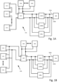
- Power system 10a includes multiple wiring configurations 111.
- Each wiring configuration 111 may include one or more power sources (not shown) which may be connected to a respective power device (also not shown).
- Power sources may be AC power sources (e.g., wind turbines, photovoltaic panels coupled to microinverters or having integrated micro inverters, etc.) or sources of DC power derived from wind turbines, battery banks, photovoltaic solar panels, rectified alternating current (AC) or petrol generators for example.
- Each wiring configuration 111 may include output terminals A and B. The outputs on terminals A and B of the wiring configurations 111 may be connected in series to form a series connection of wiring configuration 111 outputs. The series connection of wiring configuration 111 outputs may be connected to input terminals C and D of a link unit 107.
- one or more wiring configuration 111 does not include power devices.
- a wiring configuration 111 of Fig. 1A or Fig. 1B includes a single power generator, or multiple power generators connected in series or parallel.
- One or more storage devices 106 may be connected to terminals E and F of link unit 107.
- Storage devices 106 may be batteries, flywheels and/or super capacitors for example.
- Terminals E and F of link unit 107 may be configurable. Configurability of terminals E and F may allow storage devices 106 to be charged from wiring configurations 111. Configurability of terminals E and F may allow system power devices 109 to be discharged into load 104 via system power devices 109.
- One or more system power devices 109 may be connected together with respective inputs and outputs connected in parallel. The inputs of system power devices 109 may be connected to terminals G and H of link unit 107. Three system power devices 109R, 109M and 109L are shown with respective inputs and outputs connected in parallel.
- system power devices 109 may be connected to load 104 and/or multiple loads 104.
- System power devices 109 may be DC to AC inverters and load 104 may be an AC utility grid for example.
- system power devices 109 may be combiner boxes, and load 104 may be a utility grid or a DC to AC inverter connected to an AC utility grid.
- FIG. 1B illustrates a block diagram of a power system 10b, according to illustrative aspects of the disclosure.
- Power system 10b may be similar to power system 10a except with respect to wiring configurations 111.
- each wiring configuration 111 may include output terminals A and B.
- the outputs on terminals A and B of the wiring configurations 111 may be connected in parallel to form a parallel connection of wiring configuration 111 outputs.
- the parallel connection may be connected to input terminals C and D of a link unit 107.
- a feature of link units 107 may be to include a power device such as power devices 103 (which will be described in Fig. 1C ) which may convert power bi-directionally.
- a first direction of power conversion by a power device may be when multiple storage devices 106 are sourced with converted power from the power devices.
- Storage devices 106 may receive converted power from the power devices when storage devices 106 are being charged.
- a second direction of power conversion may be when power from storage devices 106 is converted by the power device to be supplied to loads 104 via system power devices 109.
- Three system power devices 109R, 109M and 109L may be shown with respective inputs and outputs connected in parallel.
- a first direction of power conversion by the inverters may be from AC to DC.
- the first direction may be for when multiple storage devices 106 are sourced with converted power from load 104 which may be an AC utility grid, for example.
- a second direction of power conversion may be used when power from storage devices 106 is converted by inverters to be supplied to loads 104 via system power devices 109.
- the second direction of power conversion may also include power from power sources 101 with respective power device 103.
- FIG. 1C illustrates more details of wiring configurations 111 shown in Figs. 1A and 1B , according to illustrative aspects of the disclosure.
- Multiple strings ST n may be shown in a wiring configuration 111 which are connected in parallel at terminals A and B.
- the output of wiring configuration 111 at terminals A and B may connect to the input of link unit device 107 at terminals C and D.
- Each wiring configuration 111 may include one or more power sources 101 which may be connected to a respective power device 103 at terminals W and X.
- the outputs of power devices 103 at terminals Y and Z may be connected together to form a string ST n which connects across terminals A and B.
- both wiring configurations 111 and power sources 101 /power devices 103 contained in a wiring configuration 111 may be connected various series/ parallel or parallel series combinations.
- Power sources 101 may contain different types of power derived from both renewable energy sources such as from sunlight, wind or wave power.
- Power sources 101 may include non-renewable energy sources such as fuel used to drive turbines or generators, for example.
- Fig. 1D illustrates circuitry which may be found in a power device such as power device 103, according to illustrative aspects of the disclosure.
- Input and output terminals W, X, Y and Z may provide connection to power lines 120 of Fig. 1C .
- power device 103 may include power circuit 135.
- Power circuit 135 may include a direct current-direct current (DC/DC) converter such as a Buck, Boost, Buck/Boost, Buck+Boost, Cuk, Flyback and/or forward converter, or a charge pump.
- power circuit 135 may include a direct current-alternating current (DC/AC) converter (also known as an inverter), such as a micro-inverter.
- DC/AC direct current-alternating current
- Power circuit 135 may have two input terminals and two output terminals, which, according to some aspects of the disclosure, may be the same as the input terminals and output terminals of power device 103.
- power device 103 may include Maximum Power Point Tracking (MPPT) circuit 138, configured to extract increased power from a power source.
- MPPT Maximum Power Point Tracking
- power circuit 135 includes MPPT functionality (e.g., power circuit 135 may be operated to draw maximum or increased power from a power source connected to power circuit 135), and a separate MPPT circuit 138 is not used.
- MPPT circuit 138 (or power circuit 135) may implement impedance matching algorithms to extract increased power from a power source.
- Power device 103 may further include a controller 105 such as an analog control circuit, a microprocessor, Digital Signal Processor (DSP), Application-Specific Integrated Circuit (ASIC) and/or a Field Programmable Gate Array (FPGA).
- DSP Digital Signal Processor
- ASIC Application-Specific Integrated Circuit
- FPGA Field Programmable Gate Array
- controller 105 may control and/or communicate with other elements of power device 103 over common bus 190.
- power device 103 may include circuitry and/or sensors/sensor interfaces 125 configured to measure parameters. Sensors/sensor interfaces 125 may measure directly or receive measured parameters from other connected sensors and/or sensor interfaces 125. The sensors and/or sensor interfaces 125 may be configured to measure parameters on or near power source 101, such as the voltage and/or current output by power source 101 and/or the power output by power source 101.
- power source 101 may be a photovoltaic (PV) generator which includes PV cells. Power sources 101 may also include a sensor or sensor interface which may directly measure or receive measurements of the irradiance received by the PV cells. The sensor or sensor interface may also directly measure or receive the temperature on or near the PV generator.
- PV photovoltaic
- power device 103 may include communication interface 129, configured to transmit and/or receive data and/or commands from other devices.
- Communication interface 129 may communicate using Power Line Communication (PLC) technology, acoustic communications technology, or additional technologies such as ZIGBEE TM , Wi-Fi, BLUETOOTH TM , near field communication (NFC), cellular communication or other wireless methods.
- Power Line Communication (PLC) may be performed over power lines 120 between power devices 103 and link unit (e.g. DC-DC converter and/or inverter) 107 which may include a similar communication interface to communication interface 129.
- link unit e.g. DC-DC converter and/or inverter
- power device 103 may include memory device 123, for logging measurements taken by sensor(s)/sensor interfaces 125, for storing code, operational protocols or other operating information.
- Memory device 123 may be flash, Electrically Erasable Programmable Read-Only Memory (EEPROM), Random Access Memory (RAM), Solid State Devices (SSD) or other types of appropriate memory devices.
- EEPROM Electrically Erasable Programmable Read-Only Memory
- RAM Random Access Memory
- SSD Solid State Devices
- power device 103 may include safety devices 170 (e.g. fuses, circuit breakers and Residual Current Devices (RCD)).
- Safety devices 170 may be passive or active.
- safety devices 170 may include one or more passive fuses disposed within power device 103.
- the element of the fuse may be designed to melt and disintegrate when excess current above the rating of the fuse flows through it. The fuse melting and disintegrating may therefore disconnect part of power device 103, from power lines 120 and/or power sources 101 for example, so as to avoid damage to power device 103.
- safety devices 170 may include active disconnect switches, configured to receive commands from a controller (e.g. controller 105, or an external controller).
- the commands received may short-circuit and/or disconnect portions of power device 103.
- the commands received may enable short-circuit and/or disconnect portions of power device 103 in response to a measurement measured by a sensor.
- the measurement may be obtained by sensors/sensor interfaces 125.
- power device 103 may include auxiliary power circuit 172.
- Auxiliary power circuit 172 may be configured so as to receive power from a power source connected to power device 103.
- Auxiliary power circuit 172 may be configured so as to provide output power suitable for operating other circuitry components (e.g. controller 105, communication interface 129, etc.). Communication, electrical connecting and/or data-sharing between the various components of power device 103 may be carried out over common bus 190.
- auxiliary power circuit 172 may be connected to an output of a power device 103 and designed to receive power from power sources connected to other power devices.
- Power device 103 may include or be operatively attached to a maximum power point tracking (MPPT) circuit (e.g. a separate MPPT circuit 138 or implemented as part of power circuit 135 ).
- the MPPT circuit may also be operatively connected to controller 105 or another controller 105 included in power device 103 which may be designated as a primary controller.
- a primary controller in power device 103 may communicatively control one or more other power devices 103 which may include controllers known as secondary controllers. Once a primary/secondary relationship may be established, a direction of control may be from the primary controller to the secondary controllers.
- the MPPT circuit under control of a primary and/or central controller 105 may be utilized to increase power extraction from power sources 101 and/or to control voltage.
- Control of a primary and/or central controller 105 may be utilized to increase current supplied to link unit (e.g. DC-DC converter and/or an inverter or a load) 107.
- link unit e.g. DC-DC converter and/or an inverter or a load
- no single power device 103 may be designated as a primary controller, and each power device 103 operates (or sub-groups of power devices operate) independently. Therefore, each power device 103 may operate without being controlled by a primary controller, or a primary controller may be separate from power devices 103.
- power device 103 may include bypass unit Q9 coupled between the inputs of power circuit 135 and/or between the outputs of power circuit 135.
- Bypass unit Q9 and/or power circuit 135 may be a junction box to terminate power lines 120 or to provide a safety feature such as fuses or residual current devices.
- Bypass unit Q9 may also be an isolation switch.
- Bypass unit Q9 may be a passive device, for example, a diode.
- Bypass unit Q9 may be controlled by controller 105. If an unsafe condition is detected, controller 105 may set bypass unit Q9 to ON, thereby short-circuiting the input and/or output of power circuit 135.
- each PV generator may provide an open-circuit voltage at its output terminals.
- the PV generators may be short-circuited, to provide a voltage of about zero to power circuit 135.
- a safe voltage may be maintained, and the two scenarios may be staggered to alternate between open-circuiting and short-circuiting PV generators. This mode of operation may allow continuous power supply to system control devices, as well as provide backup mechanisms for maintaining a safe voltage (e.g., operation of bypass unit Q9 may allow continued safe operating conditions).
- the power device 103 may comprise a partial group of the elements illustrated in Fig. 1D .
- a power device 103 might not include power circuit 135 (e.g., power circuit 135 may be replaced by a short circuit, and a single bypass unit Q9 may be featured).
- power device 103 may be still used to provide safety, monitoring and/or bypass features.
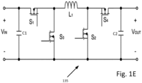
- Fig. 1E shows a buck+boost circuit implementation for power circuit 135, according to one or more illustrative aspects of the disclosure.
- the buck+boost circuit implementation for power circuit 135 utilizes metal oxide semi-conductor field effect transistors (MOSFETs) for switches S1, S2, S3 and S4.
- MOSFETs metal oxide semi-conductor field effect transistors
- the sources of switches S1, S2, S3 and S4 may be referred to as first terminals.
- the drains of S1, S2, S3 and S4 may be referred to as second terminals.
- the gates of S1, S2, S3 and S4 may be referred to as third terminals.
- Capacitor C1 may be connected in parallel across the respective positive (+) and negative (-) input terminals of the buck+boost circuit where the voltage may be indicated as V IN .
- Capacitor C2 may be connected in parallel across the respective positive (+) and negative (-) output terminals of the buck+boost circuit where the voltage may be indicated as V OUT .
- First terminals of switches S3 and S2 may connect to the common negative (-) output and input terminals of the buck+boost circuit.
- a second terminal of switch S1 may connect to the positive (+) input terminal and a first terminal of switch S1 may connect to a second terminal of switch S3.
- a second terminal of switch S4 may connect to the positive (+) output terminal and a first terminal of switch S4 may connect to the second terminals of switch S2.
- Inductor L1 may connect respectively between the second terminals of switches S3 and S4.
- Third terminals of switches S1, S2, S3 and S4 may be operatively connected to controller 105.
- Switches S1, S2, S3 and S4 may be implemented using semi-conductor devices, for example, metal oxide semiconductor field effect transistors (MOSFETs), insulated gate bipolar transistors (IGBTs), bipolar junction transistors (BJTs), Darlington transistor, diode, silicon-controlled rectifier (SCR), Diac, Triac or other types of semi-conductor switches.
- MOSFETs metal oxide semiconductor field effect transistors
- IGBTs insulated gate bipolar transistors
- BJTs bipolar junction transistors
- SCR silicon-controlled rectifier
- Diac Triac or other types of semi-conductor switches.
- switches S1, S2, S3 and S4 may be implemented by use of bipolar junction transistors.
- the collectors, emitters and bases of the bipolar transistors may refer to first terminals, second terminals and third terminals described and defined above.
- Switches S1 , S2, S3 and S4 may be implemented using mechanical switch contacts, such as hand operated switches or electro-mechanically operated switches such as relays.
- power device 103 may include, for example, a buck circuit, a boost circuit, a buck/boost circuit, a Flyback circuit, a Forward circuit, a charge pump, a Cuk converter or any other circuit which may be utilized to convert power on the input of power device 103 to the output of power device 103.
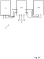
- FIG. 1F shows a plan view of a physical layout for three system power devices 109R, 109M and 109L, according to one or more illustrative aspects of the disclosure. Cables for connection of DC and AC between power devices 109R, 109M, 109L and junction box 150 are not shown.
- Power devices 109R, 109M and 109L may be mounted to a wall or a frame (both not shown). The mounting may be such that power device 109L is mounted laterally to the left (L) of middle (M) power device 109M and power device 109R is mounted laterally to the right (R) of middle (M) power device 109M.
- Junction box 150 may be shown attached underneath power device 109M but also may be attached underneath power devices 109R and/or 109L or laterally to the sides of either power devices 109R, 109M or 109L.
- an arrangement of power devices 109 may be such that power device 109L is mounted longitudinally above middle power device 109M and power device 109R is mounted longitudinally below middle power device 109M.
- junction box 150 may be mounted laterally to the left or right of middle power device 109M or to the left or right of power device 109R and/or power device 109L.
- Middle (M) power device 109M as with power devices 109L and 109R may include a data connection 14, gland 12 for an AC output cable (not shown) and gland 16 for a DC input from cables (not shown) from link units 107.
- a cable gland like glands 12, 16 and 19 in descriptions which follow may refer to devices designed to attach and secure the end of an electrical cable to the housings of power devices 109R, 109M and 109L and junction box 150.
- Middle (M) power device 109M and/or power devices 109L and 109R may also include a display 152 which is shown mounted on the housing of middle (M) power device 109M. Attached to middle (M) power device 109M and/or the wall or the frame is a junction box 150.
- the attachment of middle (M) power device 109M to junction box 150 may also include conduits 18a and 18b which may provide a mechanical attachment between power device 109M and junction box 150.
- the mechanical attachment may provide a tube for protecting electrical wiring conductors between device 109M and optional junction box 150.
- Junction box 150 may also include an isolation switch 154 and glands 12L, 12M, 12R and AC output via gland 19. The isolation switch 154 may be utilized to isolate DC from being applied to the inputs of power devices 109R, 109M and 109L.
- an installer may attach and secure a DC cable from link units 107 to the housing of power devices 109 via glands 16 .
- the conductors of the DC cable may pass through gland 16 to be terminated inside the power device 109.
- the DC cable from link units 107 may be attached and secured to the housing of power device 109M via gland 16 of power device 109M.
- the conductors of the DC cable may then be fed through conduits 18a and/or 18b and terminated into a termination inside junction box 150.
- DC inputs to power devices 109L and 109R may be provided by DC cables secured and attached between glands of junction box 150 and glands 16 of power devices 109L and 109R.
- the conductors of the DC cable may be terminated in power devices 109L and 109R and the other ends of the conductors terminated in junction box 150 at the termination inside.
- DC input into power device 109M may be via conductors from the termination via the isolation switch 154 through conduits 18a and/or 18b and terminated in power device 109M.
- the terminations of DC cables and conductors described above may also be made in additional junction/ connection boxes.
- a three phase AC cable may be attached and secured at both ends of the three phase AC cable.
- the three phase AC cable may be attached and secured at both ends for example between gland 12 of power device 109L and gland 12L of junction box 150.
- the conductors of the three phase AC cable may be terminated inside the respective housings of power device 109L and junction box 150.
- a three phase AC cable may be attached and secured at both ends of the three phase AC cable. Both ends of the three phase AC cable may be between gland 12 of power device 109R and gland 12R of junction box 150.
- the conductors of the three phase AC cable may be terminated inside the respective housings of power device 109R and junction box 150.
- a three phase AC cable may be attached and secured at both ends of the three phase AC cable for example between gland 12 of power device 109M and gland 12M of junction box 150.
- the three-phase connection between power device 109M and junction box 150 may have conductors pass through conduits 18a and/or 18b.
- the conductors provide the connection between power device 109 and junction box 150.
- An AC cable with conductors terminated in junction box 150 may be attached and secured to the housing of junction box 150 by gland 19.
- the AC cable may provide the AC combined power output of power devices 109R, 109M and 109L which may be connected to load 104.
- Power device 109 may be used to implement power devices 109R, 109M and 109L. As such, power devices 109R and 109L may or may not include display 152 as shown in Fig. 1F for example and/or other components of power device 109. Power device 109M may include all the components of power device 109. Power devices 109L and 109R may include power switching circuitries 160, sensors and/or sensor interfaces 164. Power device 109M provides the other features of power device 109 to power devices 109L and 109R.
- power device 109 may be used to implement power devices 109R, 109M and 109L.
- Controller 162 of power device 109M may serve as a master controller to the other controllers 162 of power devices 109L and 109R.
- junction box 150 may be integrated into system power device 109. In some locales, safety features included injunction box 150 are not required, and junction box 150 provides power combining circuitry (e.g. by providing connections to AC power outputs of system power devices 109L-109R) without safety devices).
- Power device 109 may include a controller 162 which provides an output to control the operation of power switching circuitry 160.
- Power switching circuitry 160 as a DC to AC inverter may have a DC input applied at terminals DC+ and DC- and a 3-phase output on terminals L1, L2 and L3.
- Terminals L1, L2 and L3 may include Neutral ( N ) and earth ( E ) terminals.
- Inverter topologies for the DC to AC inverter may include half and full bridge inverters, a diode clamped multilevel inverter, flying capacitors multilevel inverters and/or a cascaded H-bridge multilevel inverters.
- Sensor interface 164 may be operatively attached to power switching circuitry 160 and to controller 162.
- Sensor interface 164 may include sensors 164a and 164b and other sensors. Sensors 164a and 164b and the other sensors of sensor interface 164 may provide a sense of electrical parameters such as DC voltage and/or current input on the DC at terminals DC+ and DC. The sense of electrical parameters may include the AC the three phase voltages of the three-phase output on terminals L1, L2 and L3.
- the sense of electrical parameters may further include phase differences between three phase voltages on terminals L1, L2 and L3, frequencies of three phase voltages on terminals L1 , L2 and L3, total harmonic distortion (THD) on three phase voltages on terminals L1, L2 and L3, power factors of three phase voltages on terminals L1, L2 and L3, temperature of heatsinks and/or switching devices utilized in power switching circuitry 160.
- TDD total harmonic distortion
- Controller 162 may connect bi-directionally to Maximum Power Point Tracking (MPPT) circuit 169.
- MPPT circuit 169 may be configured to extract increased power from the output of link unit 107 at terminals G and H with respect to Figs. 1A and 1B for example.
- MPPT circuit 169 may implement impedance matching algorithms to extract increased power from a power source.
- Controller 162 may further include a microprocessor/ microcontroller, Digital Signal Processor (DSP), Application-Specific Integrated Circuit (ASIC) and/or a Field Programmable Gate Array (FPGA).
- DSP Digital Signal Processor
- ASIC Application-Specific Integrated Circuit
- FPGA Field Programmable Gate Array
- MPPT circuit 169 may be implemented as part of power switching circuitry 160, or might not be implemented at all (e.g. if MPPT functionality is not needed or desired, for example, if MPPT is applied by a power device connected between the (e.g., DC) input to system power device 109 and a power source.
- Controller 162 and the other components of power device 109 may also receive an operating power from auxiliary power circuit 163.
- the other components of power device 109 may include communication interface 166 and MPPT circuit 169, etc.
- Controller 162 and the other components of power device 109 may be configured to receive power from a power source connected to link unit 107.
- auxiliary power circuit 163 may be designed to receive power from power sources connected to other power devices and power converters, and/or auxiliary power circuit 163 may be designed to receive power from an electric grid.
- Controller 162 may include a microprocessor or microcontroller which may be connected bi-directionally to memory 168 and communications interface 166.
- Communications interface 166 may communicate between power devices 109M, 109L and 109R using power line communication (PLC) technology, acoustic communications technology, or additional technologies such as ZIGBEE TM , Wi-Fi, BLUETOOTH TM , near field communication (NFC), cellular communication or other wireless methods.
- Power Line Communication (PLC) may be performed over power lines between power devices 103/ power devices 109M, 109L and 109R and link units 107.
- Communication interface 166 may be a similar communication interface to communication interface 129 as described above.
- Communication interface 166 may provide communications between power devices 109M, 109L and 109R described below in further detail.
- Communication interface 166 may provide a connection to a local network and/or a cellular network.
- the connection may be also to an internet connection to and/or between power devices 103/ power devices 109M, 109L and 109R and link units 107.
- the components of power systems 10a and 10b may include power devices 103/ power devices 109M, 109L and 109R and link units 107 for example.
- the connectability to the local network and/or a cellular network may be remote and/or via a mobile computing device.
- the mobile computing device may be in the proximity of the components of power systems 10a and 10b which may allow an access to the components.
- the access may include, for example, updates of firmware to the components, remote and/or local monitoring of each component in power systems 10a and 10b for example.
- the access may additionally include real time re-configuration of the components responsive to monitored parameters sensed by sensors 125 and sensors/sensor interface 164 of power device 109.
- the access may help to establish the identity and topographical location of a component relative to other components according to detailed descriptions which follow.
- Fig. 2A shows a more detailed view of the inside contents of a junction box 250.
- the inside contents may include components which connect via cables and/or conduits to power devices 109L, 109M, 109R, according to one or more illustrative aspects of the disclosure.
- Deutsches Institut für Normung (DIN) rail 208 may be mounted to the back panel of junction box 250.
- DIN rail 208 may be further utilized to mount DC circuit breakers 206, isolation switch 254 and AC circuit breakers 204.
- Another DIN rail 208 is shown which shows two terminal blocks 264 which may be utilized to terminate both AC and DC conductors.
- Further mounted to the back panel of junction box 250 may be ground terminal 200 which may connect electrically to DIN rail 208.
- ground terminal 200 may connect to the earth ( E ) of AC circuit breaker 204, and according to some aspects, ground terminal 200 may connect to a separate earth terminal, or might not be connected to any earth terminal (e.g., where the DC power input to junction box 250 is "floating" with respect to the AC output of junction box 250 ).
- the housings of junction box 250 and/or power devices 109R, 109M and 109L may conform to the standard of a Class II or double insulated housing.
- An example of the Class II or double insulated housing may be according to International Standard IEC 61140 or Standard BSI BS 2754; Memorandum: "Construction of Electrical Equipment for Protection against Electric Shock").
- junction box 250 compliance of the housings to Class II may provide for the option of not having an electrical connection between ground terminal 200 and electrical earth ( E ). Similar safety consideration with respect Class II may also apply to the housings of other component parts included in power systems 10a and 10b such as link units 107, storage devices 106 and wiring configurations 111 for example.
- Additional terminal blocks 264 may also be mounted on DIN rail 208 and/or the back panel/ sides of junction box 250. The additional terminal blocks 264 may be added in order to expand the terminals provided by DC circuit breakers 206, isolation switch 254 and AC circuit breakers 204. Wire 265 connects terminal blocks 264 to AC circuit breakers 204.
- DC conductors DC+ and DC- from a cable attached and secured to a link unit 107 for example are shown coming through a conduit and terminated in the input of isolation switch 254. The other end of the cable may be secured and attached to power device 109M by gland 16 of power device 109M.
- the output of isolation switches 254 may be terminated on the DC+ and DC- input of DC circuit breakers 206.
- the AC three phase power output of power device 109M may be via conductors live L1 , live L2, live L3, neutral N and Earth ( E ) through conduit 18b and may be terminated in corresponding terminals of AC circuit breaker 204.
- the AC three phase power output of power device 109M may be connected by an AC three phase cable between gland 12 of power device 109M and gland 12M of junction box 250.
- the conductors of the AC three phase cable may be terminated respectively in terminals L1, L2, L3, neutral (N) and Earth (E) terminals of power device 109M and in corresponding input terminals of AC circuit breaker 204.
- the AC three phase power output of power device 109L may be connected by an AC three phase cable between gland 12 of power device 109L and gland 12L of junction box 250.
- the AC three phase power output of power device 109R may be connected by an AC three phase cable between gland 12 of power device 109R and gland 12R of junction box 250.
- the output of AC circuit breaker 204 may therefore provide the AC combined power outputs of power devices 109R, 109M and 109L.
- the output of AC circuit breaker 204 may be connected to load 104 via a three-phase cable secured and attached to the housing of junction box 250 by gland 19.
- One advantage of AC combined power outputs of power devices 109R, 109M and 109L and the mounting of 109R, 109M and 109L onto a frame and/or a wall may be to aid in the installation by a single operative.
- a single power device 109 which provides the same combined AC power output as power devices 109R, 109M and 109L, may be bulker and/or heavier.
- the single power device may require multiple operatives and /or additional lifting equipment to mount the single power device 109 on onto a frame and/or a wall.
- Another benefit of having modular inverters provides flexibility in increasing or reducing the size of a photovoltaic PV installation by simplifying and reducing the work in adding or removing inverters.
- having multiple modular inverters provides an increased level of reliability. Many photovoltaic PV installations may be operated at less than peak-production capacity for significant periods of time. In case a single system power device (e.g., inverter) malfunctions, the other two system power devices may continue to operate. The other two system power devices may provide at least two-thirds (and potentially more, depending on current system generation capacity) of the power otherwise provided by the three system power devices.
- inverter e.g., inverter
- Fig. 2B shows a more detailed view of the AC three phase connections made injunction box 250, according to one or more illustrative aspects of the disclosure.
- Power device 109L may be mounted/ positioned laterally to the left (L) of middle (M) power device 109M and power device 109R may be mounted/ positioned laterally to the right (R) of middle (M) power device 109M.
- Each power device 109R, 109M and 109L has a three-phase output on terminals L1, L2 and L3. Connections between the three-phase output on terminals L1, L2 and L3 of each power device 109R, 109M and 109L and junction box 250 may be by AC three-phase cables as described above with respect to the descriptions of Fig. 1F .
- additional terminal blocks 264 may also be mounted on DIN rail 208 and /or the back panel/ sides of junction box 250.
- the additional terminal blocks 264 may be added in order to expand the terminals provided by DC circuit breakers 206, isolation switch 254 and/or AC circuit breakers 204.
- the additional terminal block may enable the swapping of the phases of the conductors terminated in additional terminal blocks 264.
- the conductors of the AC three phase cables may be terminated at one end in respective terminals L1, L2 and L3 of each power device 109R, 109M and 109L.
- the other ends of the AC three phase cables conductors may be terminated in terminals labelled as L1, L2 and L3 provided in junction box 250.
- the three-phase output 25 (conductors L1, L2, L3, and not shown N ) from the other side of AC circuit breakers 204 of junction box 250 may be provided via an AC three phase cable.
- the AC three phase cable may be attached and secured to the housing of junction box 250 by gland 19.
- the AC three phase cables conductors may be terminated in terminals L1, L2 and L3 of AC circuit breakers 204.
- the additional terminal blocks 264 it may be such that L1 conductors of power devices 109R, 109M and 109L connect to the L1 terminal of AC circuit breakers 204; L2 conductors of power devices 109L and 109M connect to the L2 terminal of AC circuit breakers 204 but L3 conductor of power device 109R connects to the L2 terminal of AC circuit breakers 204; L3 conductors of power devices 109L and 109M connect to the L3 terminal of AC circuit breakers 204 but L2 conductor of power device 109R connects to the L3 terminal of AC circuit breakers 204.
- FIG. 2C shows a more detailed view of the AC three phase connections made injunction box 250, according to one or more illustrative aspects of the disclosure.
- Fig. 2C shows the same connections with respect to AC circuit breakers 204 described above but further includes proximity sensors 17a and respective targets 17b.
- Proximity sensors 17a may be configurable to detect the presence of nearby power device 109.
- two proximity sensors 17a of power device 109M may be utilized to provide a detection of power devices 109L and 109R.
- the detection may be by virtue of proximity sensor to provide a transceiver function.
- the transceiver function may be such that a reflected signal form target 17a for a signal sent by proximity sensor 17a may be received by proximity sensor 17a.
- Targets 17b may be passive or active RFID tags for example or may include along with proximity sensor 17a a near field communication (NFC).
- the NFC may be a short-range wireless connectivity standard that uses magnetic field induction to enable communication between power devices 109 when they are touched together, or brought within a few centimeters of each other.
- proximity sensors 17a and targets 17b may include capacitive proximity sensor types such as capacitive displacement sensors, doppler effect (sensor based on effect), eddy-current, inductive, magnetic, including magnetic proximity fuse.
- Optical sensors may include optical photocells (reflective), laser rangefinder, passive (such as charge-coupled devices) passive thermal infrared.
- Other types of sensor may further include radar, reflection of ionizing radiation, sonar (typically active or passive), ultrasonic sensor (sonar which runs in air), fiber optics sensor and/or Hall effect sensor.
- Proximity sensors 17a and targets 17b may be located on a surface of the housings of power devices 109L, 109M and 109R, embedded in the surface or inside of the housings of power devices 109L, 109M and 109R.
- proximity sensors 17a and targets 17b may be utilized to obtain and verify the lateral positions left (L) and right (R) of respective power devices 109L and 109R relative to middle (M) power device 109M. Obtaining and verifying the lateral positions may enable monitoring for theft or unauthorized replacement and/or repositioning of power devices 109L, 109M or 109R.
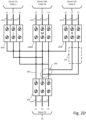
- FIG. 2D shows a more details of connections which may be made in junction box 150/250, according to one or more illustrative aspects of the disclosure.
- additional terminal blocks 264 may be added in order to expand the terminals provided by AC circuit breakers 204.
- Three terminal blocks 264L, 264M and 264R are shown labelled left ( L ), middle ( M ) and right ( R ) which may be mounted on DIN rail 208 (not shown).
- Cable-L connects electrically power device 109L to terminal block 264L
- cable-M connects electrically power device 109M to terminal block 264M
- cable-R connects electrically power device 109R to terminal block 264R.
- Glands 12L, 12M and 12R may mechanically and/ or electrically attach cable-L, cable-M and cable-R to junction box 150/250. Electrical attachment with respect to glands 12L, 12M and 12R may be with respect to wire armour/ shielding of cable-L, cable-M and cable-R.
- Each of cable-L, cable-M and cable-R includes conductors con1 , con2 and con3 which may provide phase L1, L2 and L3 respectively.
- Conductors con1 , con2 and con3 may be labelled L1, L2 and L3 and/or have respective insulation colors red (R), yellow (Y) and blue (B).
- Each of cable-L, cable-M and cable-R may further include neutral (N) and earth (E) conductors (not shown).
- Power device 109L may be located laterally to the left of power device 109M.
- a parallel connection in junction box 150/250 at terminal blocks 264L, 264M and 264R includes cable-L electrically and mechanically connecting power device l09L to power device 109M.
- power device 109R may be located laterally to the right of power device 109M and the parallel connection includes cable-R electrically and mechanically connecting power device l09R to power device 109M. Further included in the parallel connection is cable-M which connects power device 109M to power devices 109R and 109L.
- phase L1 of power device 109L terminated in terminal block 264L is substantially the same as both phases L1 of power devices 109M and 109R terminated in respective terminal blocks 264M and 264R.
- phase L2 of power device 109L terminated in terminal block 264L is substantially the same as both phases L2 of power devices 109M and 109R terminated in respective terminal blocks 264M and 264R.
- phase L3 of power device 109L terminated in terminal block 264L is substantially the same as both phases L3 of power devices 109M and 109R terminated in respective terminal blocks 264M and 264R.
- Connection between terminal blocks 264L, 264M, 264R and AC circuit breaker 204 is by wires 256 (as shown partially in Fig. 2A ).
- Connection between terminal blocks 264L, 264M, 264R and AC circuit breaker 204 may include connection of terminals L1 of terminal blocks 264L, 264M and 264R connected together and to terminal L1 of AC circuit breaker 204. Therefore, terminals and label L1 and cable con1 of AC circuit breaker 204 are the same as phases L1 of terminal blocks 264L, 264M and 264R.
- Terminals L2 of terminal blocks 264L and 264M are connected together and further connected to terminal L2 of AC circuit breaker 204.
- Connection 266 in AC circuit breaker 204 provides a swap and connection of phases L2 and L3 of terminal block 264R, therefore the three-phase output 25 via gland 19, provides phases L1, L2 and L3 on respective conductors con1 , con2' and con3' of an AC output cable (not shown) terminated in AC breaker 204 on terminals labeled respectively as L1, L2 and L3.
- Connection 266 in AC circuit breaker 204 therefore, provides the swap and connection of phases L2 and L3 of terminal block 264R.
- the labelling on the three-phase output 25 means that Phase L1 is the same phase, label, terminal throughout junction box 150/250.
- phases/ terminals/ labels of L2 and L3 on three-phase output 25 are not the same as phases/ terminals/ labels of L2 and L3 of terminal block 264R since connection 266 in AC circuit breaker 204 provides the swap and connection of phases L2 and L3 of terminal block 264R.
- a phase swap relay 267 (shown by dotted box) may be utilized to swap phases L2 and L3.
- terminals/ labels/ phases L1, L2 and L3 are substantially the same on terminal blocks 264L, 264M, 264R and AC circuit breaker 204.
- a second switch state of phase swap relay 267 may provide the swap of phases L2 and L3 of terminal block 264R according to connection 266 in AC circuit breaker 204 in the description described above.
- the description above and ones below swaps phases L2 and L3, however, swaps may be between phases L1 and L3 or between phases L1 and L2.
- Fig.3 shows a flowchart of a method 300, according to one or more illustrative aspects of the disclosure.
- an installer may mount power devices 109R, 109M and 109L to a wall or a frame (both not shown) such that power device 109L is mounted laterally to the left (L) of middle (M) power device 109M and power device 109R is mounted laterally to the right (R) of middle (M) power device 109M.
- a parallel connection may be provided which may include the termination of the AC three phase cables conductors inside power devices 109R, 109M and 109L and junction box 250 by an installer. Whereas, the feature of swapping two of the phases may already be provided in junction box 250 supplied to an installer.
- the parallel connection may be by the installer using a wiring diagram so that the parallel connection may be as described in Figs. 2B , 2C and 2D .
- the parallel connection may include a parallel connection of the DC+ and DC- connection of the inputs of power devices 109R, 109M and 109L and/or a parallel connection of the AC outputs of power devices 109R, 109M and 109L.
- the wiring diagram may be a simple visual representation of the physical connections such as cables terminations and physical layout which may include the components of power devices 109R, 109M, 109L and junction box 250.
- the wiring diagram may also show how the electrical wires or conductors are interconnected inside power devices 109R, 109M, 109L as they relate to the components of junction box 250.
- the components of junction box 250 may include DC circuit breakers 206, isolation switch 254, terminal blocks 264 and AC circuit breakers 204 shown in Fig. 2A for example.
- Conductors of AC cables may be labelled as L1, L2 and L3 or may color coded such that L1, L2 and L3 correspond respectively red, yellow and blue for example.
- junction box 250 terminates the AC cable between power device 109R and the terminals of AC circuit breakers 204. Termination of the AC cable is such that conductors L2 and L3 of the cable are terminated in respective terminals L3 and L2 of AC circuit breakers 204.
- terminals provided by AC circuit breakers 204 labelled as phases L2 and L3 swap respective phases L3 and L2 of the conductors of the cable.
- the L1 conductor of junction box 250 is connected to the L1 terminal of each of system power devices 109L-109R.
- the L2 conductor of junction box 250 is connected to the L2 terminal of system power devices 109L and 109M, but to the L3 terminal of system power device 109R.
- the L3 conductor of junction box 250 is connected to the L3 terminal of system power devices 109L and 109M, but to the L2 terminal of system power device 109R. Arranging the phase connections in this manner may provide certain benefits, as will be described below.
- Method 400 describes the operation of a parallel connection of power devices 109L, 109M and 109R where the respective DC inputs of power devices 109L, 109M and 109R are connected together and the respective three phase AC outputs of power devices 109L, 109M and 109R are connected together.
- Method 400 may be carried out by multiple controllers.
- the combined DC input to power devices 109L, 109M and 109R from link units 107 may be terminated at terminals DC+ and DC- of DC circuit breakers 206 for example.
- the combined DC input may pass through DC circuit breakers 206 and isolation switch 254 and into the parallel connected DC input of power devices 109L, 109M and 109R.
- a total DC input power of 99 Kilo Watt (KW) into the parallel connected DC input to power devices 109L, 109M and 109R.
- each of power devices 109L-109R might be connected to a separate DC power source (e.g. a photovoltaic generator or a battery) with the AC outputs of power devices 109L-109R combined in parallel.
- a separate DC power source e.g. a photovoltaic generator or a battery
- each power device 109L, 109M and 109R may convert 33KW of DC power input to a 33KW three phase AC output from each power device 109L, 109M and 109R.
- a combined three phase AC output of substantially 99KW provided on terminals L1 , L2 and L3 of AC circuit breakers 204 may be provided by virtue of the parallel connection of the respective three phase AC outputs of power devices 109L, 109M and 109R.
- a parameter such as phase difference between phases L1, L2 and L3 is sensed by sensor 164b / sensor interface 164 of power device 109M at step 403.
- phases L2 and L3 being previously swapped in junction box 250 at step 305, of method 300, different parameters are measured at the power devices.
- the results of sensing step 403 may be shown in Table 1 below: Table 1 Power converter L1-L2 Phase difference L1-L3 Phase difference Sign (L1-L2) 109L 120 -120 1 109M 120 -120 1 109R -120 120 -1
- the right (R) power device 109R always has an opposite Sign (L1-L2) with respect to the other two power devices 109M and 109L.
- the lateral positions left (L) and right (R) of respective power devices 109L and 109R relative to middle (M) power device 109M can be obtained.
- the lateral position obtained for example may be by remote monitoring techniques where communications interfaces 166 may be connectable to a local network and/or a cellular network.
- the connection to a local network and/or a cellular network may be in order to establish an internet connection to and/or between power devices 103 / power devices 109M, 109L and 109R and link units 107 for example.
- a sensed parameter (e.g. phase difference) sensed by each system power device 109 is transmitted to a central controller.
- the sensed parameter may also be the phase sequence of the phases.
- the phase sequence may be defined as the order in which the three phase voltages ( L1 , L2 and L3 or respectively red (R), yellow (Y) and blue (B)) attain their positive peak values.
- the phase sequence is said to be RYB if R phase attains its peak or maximum value first followed by Y phase 120° later and B phase 240° later than the R phase.
- the phase sequence is said to be RBY if R phase is followed by B phase 120° later and Y phase 240° (or - 120°) later than the R phase.
- RYB may be considered as positive while the sequence RBY may be considered as negative.
- the central controller may establish the positions of the power devices.
- each system power device may, based on the measurements, establish its (i.e., the instant system power device's) position and transmit the established position to the central controller.
- Step 405 may additionally consider the serial number of power device 109M in order to verify the lateral positions left (L) and right (R) of respective power devices 109L and 109R relative to middle (M) power device 109M.
- phase differences in conjunction as summarized in Tables 1 and 2 above and/or with the use of proximity sensors 17a and respective targets 17b may be used to obtain and verify the lateral positions left (L) and right (R) of respective power devices 109L and 109R relative to middle (M) power device 109M.
- phases L2 and L3 may be swapped with respect to power device 109L or 109M, or instead of swapping phases L2 and L3, phases L1 and L2 may be swapped.
- Fig. 4B shows an implementation of step 405 of method 400, according to illustrative features.
- the identifying information of the middle system power device 109M may be determined, for example, by being unique compared to the other two system power device identifying information.
- a system power device 109M may have a serial number similar to MPCxxxxx (where each 'x' is replaced by a number) and system power devices 109L and 109R may have serial numbers similar to SPCxxxxx.
- System power devices 109L and 109R may be generic, e.g., during manufacturing a position (right or left) with regard to a middle system power device which might not be predetermined.
- the device carrying out step 405 may compare the phase difference between phases L2 and L3 of the first power device to the phase difference between phases L2 and L3 of the middle power device as determined at step 406.
- Each power device of the middle, first and second power devices may calculate the L2-L3 phase difference by comparing the time elapsed between reaching the peak of the sine wave generated at phase L2 and reaching the peak of the sine wave generated at phase L3.
- the power device may determine that a 120-degree phase shift 1 50 Hz ⁇ 3 ⁇ 6.67 msec exists between phases L2 and L3. If a power device determines that about 13.33 milliseconds elapse between phase L2 reaching a peak and phase L3 reaching a peak, the power device may determine that a minus 120-degree phase shift 1 ⁇ 2 50 Hz ⁇ 3 ⁇ 13.33 msec exists between phases L2 and L3.
- the central controller determines that the L2-L3 phase difference of the first power device is substantially the same as the L2-L3 phase difference of the middle power device (e.g., both phase differences are about 120 degrees, or both phase differences are about -120 degrees).
- the central controller may proceed to step 410 and establish that the first power device is to the left of middle power device and the second power device is to the right of the middle power device.
- the central controller determines that the L2-L3 phase difference of the first power device is substantially different from the L2-L3 phase difference of the middle power device (e.g., both one phase difference is about 120 degrees, and one phase difference is about -120 degrees).
- the central controller may proceed to step 412 and establish that the first power device is to the right of middle power device and the second power device is to the left of the middle power device.
- step 405 may include comparing phase sequences measured at step 404. For example, if the middle power device and the first power device both have a phase sequence of L1, L2, L3, while the second power device has a phase sequence of L1 , L3, L2.
- the central controller may determine, at step 408, that the first power device and the middle power device have about the same L2-L3 phase difference, and proceed to step 410. If the middle power device has a phase sequence of L1, L2, L3, while the first power device has a phase sequence of L1, L3, L2, the central controller may determine, at step 408, that the first power device and the middle power device have a substantially different L2-L3 phase difference, and proceed to step 412.
- system power device 109L may be substantially identical to system power device 109R, and the decision which system power device to mount on the right and which system power device to mount on the left may be arbitrarily made by an installer.
- a controller e.g., a centralized system controller included in or connected to a monitoring system
- the controller may provide an indication (e.g., on a Graphical User Interface or via a message) of the physical location of the malfunctioning device.
- method 400 may be able to provide an indication that one inverter is to the left or the right of the other the two inverters.
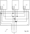
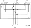
- Fig. 5A shows a part system block diagram and part schematic diagram 500 of a more detailed view of the AC three phase connections made in junction box 250, according to one or more illustrative aspects of the disclosure.
- the AC three phase connections made in junction box 250 may be in the additional terminal blocks 264 which may be added in order to expand the terminals provided by AC circuit breakers 204.
- the three-phase output 50 (conductors L1, L2, L3, N, E ) from the other side of AC circuit breakers 204 of junction box 250 may be provided via an AC three phase cable attached and secured to the housing of junction box 250 by gland 19.
- the AC three phase connections made injunction box 250 include a common neutral (N) which connects together the neutral terminals of power devices 109L, 109M and 109R together.
- the common neutral is also provided to three-phase output 50.
- Terminal L1 may be provided in the terminals of junction box 250 as the connection between L2 of power device 109L to L3 of power device 109M and L1 of power device 109R.
- Terminal L2 may be provided in the terminals of junction box 250 as the connection between L3 of power device 109L to L1 of power device 109M and L3 of power device 109R.
- Terminal L3 may be provided in the terminals of junction box 250 as the connection between L1 of power device 109L to L2 of power device 109M and L2 of power device 109R.
- the AC three phase connections made in junction box 250 may be such that auxiliary power circuits 163L, 163M, 163R and their respective power device 109L, 109M, 109R, receive an operating power from AC output phases L1 and neutral (N), L2 and N, L3 and N as opposed to operating power from one phase ( L1 for example) and neutral (N).
- the power from phases L1 and neutral (N), L2 and N, L3 and N to respective power circuits 163L, 163M, and 163R allow for a harmonic distortion as well as load sharing to be shared across phases L1, L2 and L3 as opposed to one phase.
- LVGC VDE-AR-N-4105 includes requirements related to phase balancing, frequency-based power reduction, reactive power control, inverter reconnection conditions, total harmonic distortion, power factor and output power control.
- Other international standards for grid converters may include, for example, IEEE 929-2000: Recommended Practice for Utility Interface of Photovoltaic (PV) Systems, IEC 61727; "Characteristics of the utility interface for photovoltaic (PV) systems"; International Electrotechnical Commission, IEC 61727, 2002 and EN61000-3-2-A standard for current harmonics.
- methods 300 and 400 may be applied to the AC three phase connections made injunction box 250 as shown in Fig.5A .
- circuit breakers 204 terminate the AC cable between power device 109R and the terminals of AC circuit breakers 204.
- conductors L2 and L3 of the cable are terminated in respective terminals L3 and L2 of AC circuit breakers 204.
- terminals provided by AC circuit breakers 204 labelled as phases L2 and L3 swap phases L3 and L2 of the conductors of the cable.
- the swap of phases in step 305 and subsequent operation according to the steps of method 400 allows a parameter such as phase difference between phases L1, L2 and L3 to be sensed by sensor 164b / sensor interface 164 of power device 109M at step 403 as result of the conversion of DC power to AC power at step 401.
- the results of sensing step 403 may be shown in Table 1 and 2 as shown above. Consequently, at step 405, the lateral positions left (L) and right (R) of respective power devices 109L and 109R relative to middle (M) power device 109M can be obtained for example by remote monitoring techniques.
- the remote monitoring techniques may be where communications interfaces 166 are connectable to a local network and/or a cellular network.
- the connection to a local network and/or a cellular network may be in order to establish an internet connection to and/or between power devices 103/ power devices 109M, 109L and 109R and link units 107 for example.
- Step 405 may additionally consider the serial number of power device 109M in order to verify the lateral positions left (L) and right (R) of respective power devices 109L and 109R relative to middle (M) power device 109M.
- phase differences as summarized in Tables 1 and 2 above and/or with the use of proximity sensors 17a and respective targets 17b may be used to obtain and verify the lateral positions left (L) and right (R) of respective power devices 109L and 109R relative to middle (M) power device 109M.
- Fig. 5A The connections illustrated in Fig. 5A may be summarized as shown in Table 3 below: Table 3 Power Device Device L1 is connected to output phase Device L2 is connected to output phase Device L3 is connected to output phase 109L L3 L1 L2 109M L2 L3 L1 109R L1 L3 L2
- each auxiliary power circuit 163 may draw power from the neutral (N) and power device L1 terminals, by connecting each L1 system power device terminal to a different phase of three-phase AC output 50.
- Each auxiliary power circuit 163 may also draw power between phases, for example between phase L1 and L2 or any other combination of phases.
- the total auxiliary power drawn by system power devices 109L-109R may therefore be divided evenly among the phases of three-phase AC output 50. Auxiliary power drawn evenly may improve the balance and harmonic content of three-phase AC output 50.
- system power devices 109L and 109R having different phase sequences e.g., system power device 109L having a phase sequence of L3-L1-L2 and system power device 109R having a phase sequence of L1-L3-L2).
- system power devices 109L and 109R with reference to system power device 109M may be readily determined as disclosed above.
- junction box 250 may be the same as junction box 250 of Fig. 5A , with connector terminals 520a-520c, 521a-521c, 522a-522c and 523a-523c explicitly shown.
- Connector terminals 520a-523a may be provided for connecting to a first system power device (e.g. 109L)
- connector terminals 520b-523b may be provided for connecting to a second system power device (e.g. 109 M)
- connector terminals 520c-523c may be provided for connecting to a third system power device (e.g. 109R ).
- Each connector terminal may be labeled to indicate an intended use.
- connector terminal 520a may be labeled 'N', to indicate its intended connection to a neutral terminal connector of a system power device.
- Connector terminal 521a may be labeled ' L1 ', to indicate its intended connection to an L1 terminal connector of a system power device, and so on.
- Labeling may be done using alphanumeric symbols, for example, or using different colors.
- system power devices also include labeled connector terminals
- it may be simple for an installer to connect three system power devices to junction box 250 according to the labels, with a potentially beneficial wiring scheme.
- the potentially beneficial wiring scheme may already be provided internal to junction box 250 to an installer. Use of the potentially beneficial wiring scheme may decrease the time associated with the system installation.
- Two of the phases swapped may help determine lateral positions of power converters 109 relative to each other.
- the other connection described above may also ensure total auxiliary power drawn by system power devices 109L-109R may be divided evenly among the phases of three-phase AC outputs 50.
- System power device 119M may be similar to system power device 109M, including integrating some or all of elements and/or functionality of junction box 250 of Figs. 5A-5B .
- System power device 119 may include terminals for connecting to phases L1-L3 of system power device 109L and terminals for connecting to phases L1-L3 of system power device 109R.
- the wiring arrangement combining the AC power of system power devices 109M, 119M and 109R may be implemented similarly to the arrangement shown in Fig. 2C or the arrangement shown in Fig. 5A .
- Three-phase output 50 may be output directly from system power device 119M.
- Mobile computer system 60 may be, for example, an IPHONE TM of Apple Inc., a laptop computer or a smart-phone configured to run an ANDROID TM open operating system.
- Mobile computer system 60 may be connectible over a network 624 to a server 626.
- Mobile computer system 60 may be also connectible through a cellular base station transceiver 620 to the remainder of cellular network 622.
- Mobile computer system 60 may include a processor 600 connected to local data storage 602.
- a data communications module 608 may connect processor 600 to network 624.
- a cellular communications module 604 may connect processor 600 to cellular network 622, and cellular network 622 may be further connected to the internet.
- Mobile computer system 60 may include one or more devices connected to processor 600.
- peripheral accessory devices such as a display 606, global positioning system (GPS) 610, camera 612, a microphone 614, a speaker 618, a vibrator 616, accelerometer/gravity sensor/gyroscopic sensor unit 628, BLUE-TOOTH TM , infra-red sensor (not shown).
- Display 606 may provide a graphical user interface (discussed later) to an operator for an application, which runs on mobile computing system 60.
- An operator of mobile computer system 60 may be able to operate the graphical user interface in the proximity of power devices 109 (for example power devices 109L, 109M), link units 107 and power devices 103 or remotely via an internet connection.
- the internet connection may be via a local network and/or a cellular network for example.
- FIG. 7A illustrates a graphical user interface (GUI) 700, which may include various screen portions of which may be provided on display 606 of mobile computing system 60, according to one or more illustrative aspects of the disclosure.
- GUI graphical user interface
- mobile computing system 60 and/or another computing system may be located in the vicinity of power systems 10a/10b and/or remotely via an internet connection for example.
- Screen areas 70, 71 and 71a of GUI 700 may be included on one graphical screen or be displayed on different graphical screens (e.g. depending on the screen size available).
- a touch screen may be referenced by way of example but other screens such as computer monitors may be used where items may be selected, for example, by mouse and pointer.
- screen areas 70, 71 and 71a of GUI 700 may provide upload and download of data from server 626/ network 624, a remote server as well as data from one mobile computing system 60 to another mobile computing system 60 directly.
- Upload and download of data may also be by use of communication circuits such as communication interfaces 129 and/or data communications module 608, existing communication circuits and/or a combination of retrofit communication circuits, existing communication circuits and power line communications (PLC).
- the data may include, for example, sensed and measured parameters from sensors/sensor interfaces 125/ 164 such voltages, currents, power, impedance, power factor, phase angle, harmonic distortion in phases and/or temperature.
- the data may also include, for example, configuration data or firmware upgrades for link units 107, storage devices 106, power devices 103 and power devices 109 for example.
- screen areas each may serve overall as an icon which when touched or swiped by the user using a touch screen device such as a smart phone, allows a number of sub menu options to appear.
- the sub menu may for example allow the user to view another power system or distinct separate portions of power system.
- GUI 700 may include, for example, a master screen area 70 which may give a user information as to the location of power systems 10a/10b for example.
- the local time and date an indication as to the weather conditions at the location, temperature at the location and the wind speed at the location of a power system 10a/10b .
- the local time and date may be common to each of the screen areas described below but other information may be displayed also or in addition to the local time and date for example.
- Two example menu buttons are displayed which may give two example usages of an application running on mobile computing system 60 via two menu buttons: a maintenance/ monitoring menu button, an installer's/ commissioning menu button. Other buttons may be added, such as the provision of a site management function for example.
- each of the screen areas may be presented to a user regardless of which of the two buttons is selected. However, each screen area whilst similar in appearance may present different options to the user depending on which of the two buttons is selected. Access and/or levels of access may also be provided to various screen areas by use of usernames and passwords for example.
- Screen area 71 may include (e.g., in response to the install/commissioning button being selected by a user) a partial topographical map and/or system block diagram.
- the partial topographical map and/or system block diagram may show inputs and outputs between wiring configurations 111, link units 107, storage devices 106 and power devices 109 of power systems 10a/10b for example.
- the other components of power systems 10a/10b may be revealed by swipe of a finger of the user across the screen of mobile computing device 60.
- the partial topographical map and/or system block diagram may be preloaded into mobile computing device 60. The preloading may be as a result of a design specification for power systems 10a/10b or may be added as part of a mapping algorithm used by a user/installer as they go about installing and/or commissioning components of power systems 10a/10b .
- screen 71 may allow the user/installer to enter an ID number for a component of power systems 10a/10b . How each of the components are connected to each other electrically as well as how the components are mapped in terms of location and adjacencies to each other.
- screen area 71a may be a sub screen area if a wiring configuration 111 icon is pressed.
- the sub screen may show further details of wiring configuration 111 to include a string of power devices 103 outputs, where the input of each power device 103 is connected to a power source 101 (photovoltaic panel for example).
- Screen 71a my further include ID numbers to be entered for each component, to display designed voltages (V) and currents (A) as well as for example to allow a user/installer to enter the angle of a photovoltaic (PV) panel and/or location of the PV panel/ power source 101 for example.
- Screen area 71a may (e.g., in response to the install/commissioning button being selected by a user) allow fault finding in the string by activating bypass units Q9 with respect to power devices 103. The results of the activation of bypass units Q9 may be monitored in terms of voltages (V) and currents (A) sensed by sensors/sensor interfaces 125 in screen area 71a.
- bypass units Q9 may help to identify a faulty power source 101 and/or power circuit 135 for example.
- Monitoring and operation of bypass units Q9 of the string may be when an operative is in the proximity of the components of power systems 10a and 10b with mobile computing device 60 and/or be connected to a local network and/or a cellular network. Connection to a local network and/or a cellular network may be in order to establish an internet connection to and/or between power devices 103/ power devices 109M, 109L and 109R and link units 107 for example.
- FIG. 7B illustrates a graphical user interface (GUI) 700, which may include various screen portions of graphical user interface (GUI) 700, according to one or more illustrative aspects of the disclosure.
- GUI graphical user interface
- screen area 71b may be a sub screen as a result of pressing the power device 109 icon shown by hashed lines in screen area 71. Pressing the power converter icon may reveal in screen area 71b power devices 109L, 109M, 109R and junction box 250 according to features described above with respect to the parallel connection of power devices 109L, 109M and 109R to provide a combined AC three phase output.
- Screen area 71b provides a vertical slider 72 to show further details of power device 109M (partially shown) and power device 109L (not shown). Additional operating features of junction box 250, power device 109R and power device 109M may be revealed by respective vertical sliders 72a, 72b and 72c.
- the icon for junction box 250 is pressed may allow an installer to view a wiring diagram for junction box 250 similar to Fig. 2A for example.
- the wiring diagram may show how the electrical wires or conductors to the components of junction box 250 such as DC circuit breakers 206, isolation switch 254 and how they relate to AC circuit breakers 204 for example.
- Conductors of AC cables may be labelled as L1, L2 and L3 or may color coded such that L1, L2 and L3 correspond respectively red, yellow and blue for example.
- the configuration may be when an installer with mobile computing system 60 and/or another computing system is located in the vicinity of power systems 10a/10b and/or remotely via an internet connection for example.
- the configuration for example may include configuration parameters for power devices 109L, 109M and 109R to share the power conversion by system power devices 109L, 109M and 109R to a load according to a prescribed function.
- the prescribed function may allow each system power device 109L, 109M and 109R to autonomously determine its share of power conversion.
- Each system power device 109L, 109M and 109R may then operate according to its own power conversion formula/function, such that overall the parallel connected system power devices 109L, 109M and 109R share the power conversion to a load in a predetermined manner.
- Commissioning, monitoring/ sensing may be by a user in proximity to power devices 109L, 109M and 109R or remotely connected by an internet connection.
- a user may be able to positionally locate power devices 109L, 109M and 109R lateral positions to each other and ensure that monitored or sensed parameters may be properly ascribed to each of the power devices 109L, 109M and 109R.
- Sensors 164a and 164b and the other sensors of sensor interface 164 may sense electrical parameters such as DC voltage and/or current input on the DC at terminals DC+ and DC-.
- Sensed electrical parameter may further include the AC the three phase voltages of the three-phase output on terminals L1, L2 and L3.
- Other parameters sensed by the sensors and sensors 164a and 164b may include phase differences between three phase voltages on terminals L1, L2 and L3, frequencies of three phase voltages on terminals L1 , L2 and L3, total harmonic distortion (THD) on three phase voltages on terminals L1, L2 and L3, power factors of three phase voltages on terminals L1, L2 and L3 or temperature of heatsinks and/or switching devices utilized in power switching circuitry 160.
- TDD total harmonic distortion
- One or more illustrative aspects of the disclosure herein may include a general-purpose or special-purpose computer system including various computer hardware components, which are discussed in greater detail below.
- Various aspects of the disclosure herein may also include computer-readable media for carrying or having computer-executable instructions, computer-readable instructions, or data structures stored thereon.
- Such computer-readable media may be any available media, which may be accessible by a general-purpose or special-purpose computer system.
- such computer-readable media can include non-transitory computer-readable media.
- Such computer-readable media can include physical storage media such as RAM, ROM, EPROM, flash disk, CD-ROM or other optical disk storage, magnetic disk storage or other magnetic storage devices, or any other media which can be used to carry or store desired program code mechanisms in the form of computer-executable instructions, computer-readable instructions, or data structures and which may be accessed by a general-purpose or special-purpose computer system.
- physical storage media such as RAM, ROM, EPROM, flash disk, CD-ROM or other optical disk storage, magnetic disk storage or other magnetic storage devices, or any other media which can be used to carry or store desired program code mechanisms in the form of computer-executable instructions, computer-readable instructions, or data structures and which may be accessed by a general-purpose or special-purpose computer system.
- a "computer system” may be defined as one or more software or firmware modules, one or more hardware modules, or combinations thereof, which work together to perform operations on electronic data.
- the definition of computer system may include the hardware components of a personal computer, as well as software or firmware modules, such as the operating system of the personal computer. The physical layout of the modules may be not important.
- a computer system may include one or more computers connected via a computer network.
- a computer system may include a single physical device (such as a smart-phone) where internal modules (such as a memory and processor) work together to perform operations on electronic data.
- the term "mobile computer system” especially may include laptop computers, net-book computers, cellular telephones, smart-phones, wireless telephones, personal digital assistants, portable computers with touch sensitive screens and the like.
- a "network” may be defined as any architecture where two or more computer systems may exchange data.
- the term "network” may include wide area network, Internet local area network, Intranet, wireless networks such as "Wi-Fi", virtual private networks, mobile access network using access point name (APN) and Internet.
- Exchanged data may be in the form of electrical signals that are meaningful to the two or more computer systems.
- data may be transferred, or provided over a network or another communication connection (either hard wired, wireless, or a combination of hard wired or wireless) to a computer system or computer device, the connection may be properly viewed as a computer-readable medium.
- any such connection may be properly termed a computer-readable medium.
- Computer-executable instructions include, for example, instructions and data which cause a general-purpose computer system or special-purpose computer system to perform a certain function or group of functions.
- server refers to a computer system including a processor, data storage and a network adapter generally configured to provide a service over the computer network.
- a computer system which receives a service provided by the server may be known as a "client” computer system.
- data as used herein may refer to a processed analogue signal, the processing including analogue to digital conversion into digital information accessible to a computer system.
Landscapes
- Engineering & Computer Science (AREA)
- Power Engineering (AREA)
- Inverter Devices (AREA)
Claims (3)
- Vorrichtung, umfassend:einen ersten, einen zweiten und einen dritten DC-AC-Drei-Phasen-Wechselrichter (109M, 109R, 109L), wobei jeder Wechselrichter umfasst:eine Mehrzahl von AC-Ausgangsanschlüssen, umfassend: einen Ausgangsanschluss (L1) der ersten Phase, einen Ausgangsanschluss (L2) der zweiten Phase und einen Ausgangsanschluss (L3) der dritten Phase;wobei die Vorrichtung ferner umfasst:
eine Anschlussdose (250) umfassend:eine Mehrzahl von Phasen-Eingangsanschlüssen, wobei die Mehrzahl von Phasen-Eingangsanschlüssen einen Eingangsanschluss (L1/204) der ersten Phase, einen Eingangsanschluss (L2/204) der zweiten Phase und einen Eingangsanschluss (L3/204) der dritten Phase umfasst;wobei der Eingangsanschluss (L1/204) der ersten Phase mit folgenden Anschlüssen verbunden ist:dem Ausgangsanschluss (L1) der ersten Phase des ersten Wechselrichters (109M),dem Ausgangsanschluss (L1) der ersten Phase des zweiten Wechselrichters (109R),dem Ausgangsanschluss (L1) der ersten Phase des dritten Wechselrichters (109L) undeinem Ausgangsanschluss (L1/25) der ersten Phase der Anschlussdose (250);wobei der Eingangsanschluss (L2/204) der zweiten Phase mit folgenden Anschlüssen verbunden ist:dem Ausgangsanschluss (L2) der zweiten Phase des ersten Wechselrichters (109M),dem Ausgangsanschluss (L3) der dritten Phase des zweiten Wechselrichters (109R),dem Ausgangsanschluss (L2) der zweiten Phase des dritten Wechselrichters (109L) undeinem Ausgangsanschluss (L2/25) der zweiten Phase der Anschlussdose (250); undwobei der Eingangsanschluss (L3/204) der dritten Phase mit folgenden Anschlüssen verbunden ist:dem Ausgangsanschluss (L3) der dritten Phase des ersten Wechselrichters (109M),dem Ausgangsanschluss (L2) der zweiten Phase des zweiten Wechselrichters (109R),dem Ausgangsanschluss (L3) der dritten Phase des dritten Wechselrichters (109L) undeinem Ausgangsanschluss (L3/25) der dritten Phase der Anschlussdose (250); undwobei jeder der Wechselrichter (109M, 109R, 109L) dazu ausgelegt ist, einen Phasenparameter zwischen seinen jeweiligen Phasen-Ausgangsanschlüssen (L1, L2, L3) zu erfassen, wobei der Phasenparameter einer aus Phasendifferenz und Phasensequenz ist;wobei die Vorrichtung ferner einen Controller umfasst, der dazu ausgelegt ist, die erfassten Phasenparameterdaten aus den jeweiligen Wechselrichtern zu empfangen und die relative Position des zweiten Wechselrichters (109R) bezüglich der anderen beiden Wechselrichter (109L, 109M) auf Basis der empfangenen erfassten Phasenparameterdaten zu bestimmen. - Verfahren, umfassend:Anschließen eines ersten, eines zweiten und eines dritten DC-AC-Drei-Phasen-Wechselrichters (109M, 109R, 109L) an eine Anschlussdose (250);wobei die Anschlussdose eine Mehrzahl von Phasen-Eingangsanschlüssen umfasst, wobei die Mehrzahl von Phasen-Eingangsanschlüssen einen Eingangsanschluss (L1/204) der ersten Phase, einen Eingangsanschluss (L2/204) der zweiten Phase und einen Eingangsanschluss (L3/204) der dritten Phase umfasst;wobei jeder Wechselrichter eine Mehrzahl von AC-Ausgangsanschlüssen umfasst, die einen Ausgangsanschluss (L1) der ersten Phase, einen Ausgangsanschluss (L2) der zweiten Phase und einen Ausgangsanschluss (L3) der dritten Phase umfassen;wobei das Anschließen umfasst:Verbinden des Eingangsanschlusses (L1/204) der ersten Phase der Anschlussdose (250) mit folgenden Anschlüssen:dem Ausgangsanschluss (L1) der ersten Phase des ersten Wechselrichters (109M),dem Ausgangsanschluss (L1) der ersten Phase des zweiten Wechselrichters (109R),dem Ausgangsanschluss (L1) der ersten Phase des dritten Wechselrichters (109L) undeinem Ausgangsanschluss (L1/25) der ersten Phase der Anschlussdose (250);Verbinden des Eingangsanschlusses (L2/204) der zweiten Phase der Anschlussdose (250) mit folgenden Anschlüssen:dem Ausgangsanschluss (L2) der zweiten Phase des ersten Wechselrichters (109M),dem Ausgangsanschluss (L3) der dritten Phase des zweiten Wechselrichters (109R),dem Ausgangsanschluss (L2) der zweiten Phase des dritten Wechselrichters (109L) undeinem Ausgangsanschluss (L2/25) der zweiten Phase der Anschlussdose (250);Verbinden des Eingangsanschlusses (L3/204) der dritten Phase der Anschlussdose (250) mit folgenden Anschlüssen:dem Ausgangsanschluss (L3) der dritten Phase des ersten Wechselrichters (109M),dem Ausgangsanschluss (L2) der zweiten Phase des zweiten Wechselrichters (109R),dem Ausgangsanschluss (L3) der dritten Phase des dritten Wechselrichters (109L) undeinem Ausgangsanschluss (L3/25) der dritten Phase der Anschlussdose (250); undErfassen eines Phasenparameters durch jeden der Wechselrichter (109M, 109R, 109L) zwischen seinen jeweiligen Phasen-Ausgangsanschlüssen (L1, L2, L3), wobei der Phasenparameter einer aus Phasendifferenz und Phasensequenz ist;Empfangen der erfassten Phasenparameterdaten durch einen Controller aus den jeweiligen Wechselrichtern und Bestimmen der relativen Position des zweiten Wechselrichters (109R) bezüglich der anderen beiden Wechselrichter (109L, 109M) durch den Controller auf Basis der empfangenen erfassten Phasenparameterdaten.
- Nichtflüchtiges computerlesbares Medium, auf dem Programmcode aufgezeichnet ist, der bei seiner Ausführung durch einen oder mehrere Prozessoren, die mit dem Controller der durch Anspruch 1 definierten Vorrichtung verbunden sind oder Teil von dieser sind, den einen oder die mehreren Prozessoren dazu veranlasst, das durch Anspruch 2 definierte Verfahren auszuführen.
Priority Applications (1)
| Application Number | Priority Date | Filing Date | Title |
|---|---|---|---|
| EP24162550.8A EP4358346A3 (de) | 2017-11-20 | 2018-11-19 | Bereitstellung von positionsbewusstseinsinformationen und erhöhung der stromqualität von parallel geschalteten wechselrichtern |
Applications Claiming Priority (1)
| Application Number | Priority Date | Filing Date | Title |
|---|---|---|---|
| US201762588600P | 2017-11-20 | 2017-11-20 |
Related Child Applications (1)
| Application Number | Title | Priority Date | Filing Date |
|---|---|---|---|
| EP24162550.8A Division EP4358346A3 (de) | 2017-11-20 | 2018-11-19 | Bereitstellung von positionsbewusstseinsinformationen und erhöhung der stromqualität von parallel geschalteten wechselrichtern |
Publications (2)
| Publication Number | Publication Date |
|---|---|
| EP3487059A1 EP3487059A1 (de) | 2019-05-22 |
| EP3487059B1 true EP3487059B1 (de) | 2024-03-13 |
Family
ID=64362438
Family Applications (2)
| Application Number | Title | Priority Date | Filing Date |
|---|---|---|---|
| EP24162550.8A Withdrawn EP4358346A3 (de) | 2017-11-20 | 2018-11-19 | Bereitstellung von positionsbewusstseinsinformationen und erhöhung der stromqualität von parallel geschalteten wechselrichtern |
| EP18207048.2A Active EP3487059B1 (de) | 2017-11-20 | 2018-11-19 | Bereitstellung von positionsinformationen und steigerung der stromqualität von parallel geschalteten wechselrichtern |
Family Applications Before (1)
| Application Number | Title | Priority Date | Filing Date |
|---|---|---|---|
| EP24162550.8A Withdrawn EP4358346A3 (de) | 2017-11-20 | 2018-11-19 | Bereitstellung von positionsbewusstseinsinformationen und erhöhung der stromqualität von parallel geschalteten wechselrichtern |
Country Status (3)
| Country | Link |
|---|---|
| US (4) | US10554149B2 (de) |
| EP (2) | EP4358346A3 (de) |
| CN (1) | CN109818367B (de) |
Families Citing this family (6)
| Publication number | Priority date | Publication date | Assignee | Title |
|---|---|---|---|---|
| US12395068B2 (en) * | 2017-03-29 | 2025-08-19 | Solaredge Technologies Ltd. | Bypass circuit and method to bypass power modules in power system |
| CN110277953A (zh) * | 2019-06-19 | 2019-09-24 | 宁波诺丁汉大学 | 基于变pwm频率法的永磁同步电机模块化驱动器的主动热管理方法 |
| CA3055454C (en) * | 2019-09-16 | 2026-03-31 | Weihai Xue | An apparatus, method and article for maximizing solar charge current through the use of split wire(s) in a solar array with solar panels connected in the combination of series and parallel |
| WO2021208045A1 (zh) * | 2020-04-16 | 2021-10-21 | 华为技术有限公司 | 一种电源系统 |
| CN111342464B (zh) * | 2020-04-21 | 2021-12-10 | 西安热工研究院有限公司 | 一种单母线系统接线方式机组核相的系统及方法 |
| EP3930160A1 (de) * | 2020-06-23 | 2021-12-29 | ABB Power Grids Switzerland AG | Wandler, verfahren zur installation eines leistungssystems und verwendung eines wandlers |
Citations (1)
| Publication number | Priority date | Publication date | Assignee | Title |
|---|---|---|---|---|
| CN2907018Y (zh) * | 2006-06-13 | 2007-05-30 | 邹吉学 | 直埋式交联电缆多分支接线箱 |
Family Cites Families (23)
| Publication number | Priority date | Publication date | Assignee | Title |
|---|---|---|---|---|
| US2227651A (en) | 1939-10-19 | 1941-01-07 | Bbc Brown Boveri & Cie | Electric valve control system |
| WO2003036688A2 (en) * | 2001-10-25 | 2003-05-01 | Sandia Corporation | Alternating current photovoltaic building block |
| JP2008517582A (ja) * | 2004-10-20 | 2008-05-22 | シーメンス ヴィディーオー オートモーティヴ コーポレイション | 電力システム、方法および装置 |
| US7772716B2 (en) * | 2007-03-27 | 2010-08-10 | Newdoll Enterprises Llc | Distributed maximum power point tracking system, structure and process |
| US7564703B1 (en) * | 2007-04-17 | 2009-07-21 | Rockwell Automation Technologies, Inc. | Method and apparatus for synchronized parallel operation of PWM inverters with limited circulating current |
| US20090283129A1 (en) * | 2008-05-14 | 2009-11-19 | National Semiconductor Corporation | System and method for an array of intelligent inverters |
| US8816528B2 (en) * | 2009-09-09 | 2014-08-26 | Sundial Power Pods, Llc | Mobile power system |
| US8937822B2 (en) * | 2011-05-08 | 2015-01-20 | Paul Wilkinson Dent | Solar energy conversion and utilization system |
| CN103036529B (zh) * | 2011-09-29 | 2017-07-07 | 株式会社大亨 | 信号处理装置、滤波器、控制电路、逆变器和转换器系统 |
| EP2904680B1 (de) | 2012-10-01 | 2020-04-29 | ABB Schweiz AG | Verfahren und system für die schnelle sammelschienenüberführung in einem elektrischen energiesystem |
| CN103095165B (zh) * | 2013-01-16 | 2015-09-30 | 武汉新能源接入装备与技术研究院有限公司 | 无输出隔离变压器的三相逆变器并联控制方法 |
| EP2951903B1 (de) * | 2013-01-30 | 2018-03-14 | SMA Solar Technology AG | Verfahren und wechselrichter zur leistungsverteilung über mehrere, gemeinsam an einen gleichspannungseingang eines dc/ac-wandlers angeschlossene gleichstromquellen |
| JP2015126544A (ja) | 2013-12-25 | 2015-07-06 | 東芝シュネデール・インバータ株式会社 | 三相電源の相順切替装置 |
| GB201403560D0 (en) * | 2014-02-28 | 2014-04-16 | Eltek As | Inverter system |
| US9923487B2 (en) * | 2014-04-14 | 2018-03-20 | Tmeic Corporation | Hybrid power converter for renewable energy power plant |
| WO2015194012A1 (ja) * | 2014-06-19 | 2015-12-23 | 株式会社安川電機 | マトリクスコンバータ |
| CN106464162B (zh) * | 2014-06-20 | 2019-02-19 | 通用电气公司 | 用于对多逆变器功率变换器的控制的装置及方法 |
| JP6243575B2 (ja) * | 2015-04-01 | 2017-12-06 | 東芝三菱電機産業システム株式会社 | 無停電電源装置およびそれを用いた無停電電源システム |
| US9762143B2 (en) * | 2015-04-29 | 2017-09-12 | Toshiba Mitsubishi-Electric Industrial Systems Corporation | Devices and methods for controlling current in inverters |
| CN204928190U (zh) * | 2015-08-17 | 2015-12-30 | 日月元科技(深圳)有限公司 | 太阳能逆变系统 |
| US9991778B2 (en) * | 2016-02-29 | 2018-06-05 | The Boeing Company | Balancing current within a modular converter system |
| JP6533754B2 (ja) * | 2016-03-17 | 2019-06-19 | 日立オートモティブシステムズ株式会社 | 電子制御装置及びその制御方法 |
| CN115347667B (zh) * | 2021-05-13 | 2026-04-10 | 台达电子企业管理(上海)有限公司 | 光伏逆变系统及其rsd的自动定位方法与故障控制方法 |
-
2018
- 2018-11-16 US US16/192,921 patent/US10554149B2/en active Active
- 2018-11-19 EP EP24162550.8A patent/EP4358346A3/de not_active Withdrawn
- 2018-11-19 EP EP18207048.2A patent/EP3487059B1/de active Active
- 2018-11-20 CN CN201811384661.3A patent/CN109818367B/zh not_active Expired - Fee Related
-
2019
- 2019-11-15 US US16/684,623 patent/US11418129B2/en active Active
-
2022
- 2022-07-20 US US17/869,405 patent/US12191657B2/en active Active
-
2024
- 2024-11-20 US US18/953,388 patent/US20250079885A1/en active Pending
Patent Citations (1)
| Publication number | Priority date | Publication date | Assignee | Title |
|---|---|---|---|---|
| CN2907018Y (zh) * | 2006-06-13 | 2007-05-30 | 邹吉学 | 直埋式交联电缆多分支接线箱 |
Also Published As
| Publication number | Publication date |
|---|---|
| CN109818367B (zh) | 2024-07-26 |
| EP4358346A3 (de) | 2024-07-24 |
| US20250079885A1 (en) | 2025-03-06 |
| US20200083821A1 (en) | 2020-03-12 |
| CN109818367A (zh) | 2019-05-28 |
| US10554149B2 (en) | 2020-02-04 |
| US11418129B2 (en) | 2022-08-16 |
| US12191657B2 (en) | 2025-01-07 |
| US20220360106A1 (en) | 2022-11-10 |
| EP4358346A2 (de) | 2024-04-24 |
| EP3487059A1 (de) | 2019-05-22 |
| US20190157984A1 (en) | 2019-05-23 |
Similar Documents
| Publication | Publication Date | Title |
|---|---|---|
| EP3487059B1 (de) | Bereitstellung von positionsinformationen und steigerung der stromqualität von parallel geschalteten wechselrichtern | |
| US11400821B2 (en) | Electric-vehicle charging apparatus | |
| US11965918B2 (en) | Meter for use with a distributed energy resource device | |
| US9899867B2 (en) | DC power server for a DC microgrid | |
| US9480132B2 (en) | Safety device for a street lamp system | |
| US20120019074A1 (en) | Methods and apparatus for high-frequency electrical power collection and transfer | |
| US9369062B2 (en) | Single-phase emergency operation of a three-phase inverter and corresponding inverter having a polyphase to single phase changeover operation | |
| EP3410552B1 (de) | Routing-leistung in einem stromversorgungssystem | |
| US20140077609A1 (en) | Serially connected micro-inverter system with trunk and drop cabling | |
| US12549220B2 (en) | Method and apparatus to enable communication and control in a power system | |
| CN105870955B (zh) | 用于校正hvdc系统中的电力损耗的方法 | |
| EP4199292B1 (de) | Stromquellensystem, datenzentrum und ladevorrichtung | |
| An et al. | Space vector pulse-width modulation control strategy for four-leg inverters under single line-to-ground faults in islanded microgrids | |
| EP3214748B1 (de) | Zusammenstellbarer wechselrichter | |
| CN108957217A (zh) | 交直交供电系统控制与保护方法 | |
| US20250385324A1 (en) | Reconfigurable battery energy storage system (bess) ac wiring | |
| US20240047970A1 (en) | Systems and Methods for Energy Conversion to and from an Electric Vehicle | |
| Yang et al. | Topology and control of transformerless high voltage grid-connected PV systems with a cascade step-up structure | |
| CN117713189A (zh) | 供电系统、功率变换装置及功率变换系统 |
Legal Events
| Date | Code | Title | Description |
|---|---|---|---|
| PUAI | Public reference made under article 153(3) epc to a published international application that has entered the european phase |
Free format text: ORIGINAL CODE: 0009012 |
|
| STAA | Information on the status of an ep patent application or granted ep patent |
Free format text: STATUS: THE APPLICATION HAS BEEN PUBLISHED |
|
| AK | Designated contracting states |
Kind code of ref document: A1 Designated state(s): AL AT BE BG CH CY CZ DE DK EE ES FI FR GB GR HR HU IE IS IT LI LT LU LV MC MK MT NL NO PL PT RO RS SE SI SK SM TR |
|
| AX | Request for extension of the european patent |
Extension state: BA ME |
|
| STAA | Information on the status of an ep patent application or granted ep patent |
Free format text: STATUS: REQUEST FOR EXAMINATION WAS MADE |
|
| STAA | Information on the status of an ep patent application or granted ep patent |
Free format text: STATUS: EXAMINATION IS IN PROGRESS |
|
| 17P | Request for examination filed |
Effective date: 20191122 |
|
| RBV | Designated contracting states (corrected) |
Designated state(s): AL AT BE BG CH CY CZ DE DK EE ES FI FR GB GR HR HU IE IS IT LI LT LU LV MC MK MT NL NO PL PT RO RS SE SI SK SM TR |
|
| 17Q | First examination report despatched |
Effective date: 20191218 |
|
| RIC1 | Information provided on ipc code assigned before grant |
Ipc: H02J 7/34 20060101ALN20230329BHEP Ipc: H02J 1/10 20060101ALN20230329BHEP Ipc: G01R 29/18 20060101ALN20230329BHEP Ipc: H02M 7/00 20060101ALN20230329BHEP Ipc: H02J 3/48 20060101ALI20230329BHEP Ipc: H02J 13/00 20060101ALI20230329BHEP Ipc: H02J 3/38 20060101ALI20230329BHEP Ipc: H02M 7/493 20070101AFI20230329BHEP |
|
| P01 | Opt-out of the competence of the unified patent court (upc) registered |
Effective date: 20230505 |
|
| GRAP | Despatch of communication of intention to grant a patent |
Free format text: ORIGINAL CODE: EPIDOSNIGR1 |
|
| STAA | Information on the status of an ep patent application or granted ep patent |
Free format text: STATUS: GRANT OF PATENT IS INTENDED |
|
| RIC1 | Information provided on ipc code assigned before grant |
Ipc: H02J 7/34 20060101ALN20230906BHEP Ipc: H02J 1/10 20060101ALN20230906BHEP Ipc: G01R 29/18 20060101ALN20230906BHEP Ipc: H02M 7/00 20060101ALN20230906BHEP Ipc: H02J 3/48 20060101ALI20230906BHEP Ipc: H02J 13/00 20060101ALI20230906BHEP Ipc: H02J 3/38 20060101ALI20230906BHEP Ipc: H02M 7/493 20070101AFI20230906BHEP |
|
| RIC1 | Information provided on ipc code assigned before grant |
Ipc: H02J 7/34 20060101ALN20230911BHEP Ipc: H02J 1/10 20060101ALN20230911BHEP Ipc: G01R 29/18 20060101ALN20230911BHEP Ipc: H02M 7/00 20060101ALN20230911BHEP Ipc: H02J 3/48 20060101ALI20230911BHEP Ipc: H02J 13/00 20060101ALI20230911BHEP Ipc: H02J 3/38 20060101ALI20230911BHEP Ipc: H02M 7/493 20070101AFI20230911BHEP |
|
| RIC1 | Information provided on ipc code assigned before grant |
Ipc: H02J 7/34 20060101ALN20230918BHEP Ipc: H02J 1/10 20060101ALN20230918BHEP Ipc: G01R 29/18 20060101ALN20230918BHEP Ipc: H02M 7/00 20060101ALN20230918BHEP Ipc: H02J 3/48 20060101ALI20230918BHEP Ipc: H02J 13/00 20060101ALI20230918BHEP Ipc: H02J 3/38 20060101ALI20230918BHEP Ipc: H02M 7/493 20070101AFI20230918BHEP |
|
| INTG | Intention to grant announced |
Effective date: 20231004 |
|
| GRAS | Grant fee paid |
Free format text: ORIGINAL CODE: EPIDOSNIGR3 |
|
| GRAA | (expected) grant |
Free format text: ORIGINAL CODE: 0009210 |
|
| STAA | Information on the status of an ep patent application or granted ep patent |
Free format text: STATUS: THE PATENT HAS BEEN GRANTED |
|
| AK | Designated contracting states |
Kind code of ref document: B1 Designated state(s): AL AT BE BG CH CY CZ DE DK EE ES FI FR GB GR HR HU IE IS IT LI LT LU LV MC MK MT NL NO PL PT RO RS SE SI SK SM TR |
|
| REG | Reference to a national code |
Ref country code: GB Ref legal event code: FG4D |
|
| REG | Reference to a national code |
Ref country code: CH Ref legal event code: EP |
|
| REG | Reference to a national code |
Ref country code: DE Ref legal event code: R096 Ref document number: 602018066511 Country of ref document: DE |
|
| REG | Reference to a national code |
Ref country code: IE Ref legal event code: FG4D Ref country code: NL Ref legal event code: FP |
|
| PG25 | Lapsed in a contracting state [announced via postgrant information from national office to epo] |
Ref country code: LT Free format text: LAPSE BECAUSE OF FAILURE TO SUBMIT A TRANSLATION OF THE DESCRIPTION OR TO PAY THE FEE WITHIN THE PRESCRIBED TIME-LIMIT Effective date: 20240313 |
|
| REG | Reference to a national code |
Ref country code: LT Ref legal event code: MG9D |
|
| PG25 | Lapsed in a contracting state [announced via postgrant information from national office to epo] |
Ref country code: GR Free format text: LAPSE BECAUSE OF FAILURE TO SUBMIT A TRANSLATION OF THE DESCRIPTION OR TO PAY THE FEE WITHIN THE PRESCRIBED TIME-LIMIT Effective date: 20240614 |
|
| PG25 | Lapsed in a contracting state [announced via postgrant information from national office to epo] |
Ref country code: RS Free format text: LAPSE BECAUSE OF FAILURE TO SUBMIT A TRANSLATION OF THE DESCRIPTION OR TO PAY THE FEE WITHIN THE PRESCRIBED TIME-LIMIT Effective date: 20240613 Ref country code: HR Free format text: LAPSE BECAUSE OF FAILURE TO SUBMIT A TRANSLATION OF THE DESCRIPTION OR TO PAY THE FEE WITHIN THE PRESCRIBED TIME-LIMIT Effective date: 20240313 |
|
| PG25 | Lapsed in a contracting state [announced via postgrant information from national office to epo] |
Ref country code: ES Free format text: LAPSE BECAUSE OF FAILURE TO SUBMIT A TRANSLATION OF THE DESCRIPTION OR TO PAY THE FEE WITHIN THE PRESCRIBED TIME-LIMIT Effective date: 20240313 |
|
| PG25 | Lapsed in a contracting state [announced via postgrant information from national office to epo] |
Ref country code: RS Free format text: LAPSE BECAUSE OF FAILURE TO SUBMIT A TRANSLATION OF THE DESCRIPTION OR TO PAY THE FEE WITHIN THE PRESCRIBED TIME-LIMIT Effective date: 20240613 Ref country code: NO Free format text: LAPSE BECAUSE OF FAILURE TO SUBMIT A TRANSLATION OF THE DESCRIPTION OR TO PAY THE FEE WITHIN THE PRESCRIBED TIME-LIMIT Effective date: 20240613 Ref country code: LT Free format text: LAPSE BECAUSE OF FAILURE TO SUBMIT A TRANSLATION OF THE DESCRIPTION OR TO PAY THE FEE WITHIN THE PRESCRIBED TIME-LIMIT Effective date: 20240313 Ref country code: HR Free format text: LAPSE BECAUSE OF FAILURE TO SUBMIT A TRANSLATION OF THE DESCRIPTION OR TO PAY THE FEE WITHIN THE PRESCRIBED TIME-LIMIT Effective date: 20240313 Ref country code: GR Free format text: LAPSE BECAUSE OF FAILURE TO SUBMIT A TRANSLATION OF THE DESCRIPTION OR TO PAY THE FEE WITHIN THE PRESCRIBED TIME-LIMIT Effective date: 20240614 Ref country code: FI Free format text: LAPSE BECAUSE OF FAILURE TO SUBMIT A TRANSLATION OF THE DESCRIPTION OR TO PAY THE FEE WITHIN THE PRESCRIBED TIME-LIMIT Effective date: 20240313 Ref country code: ES Free format text: LAPSE BECAUSE OF FAILURE TO SUBMIT A TRANSLATION OF THE DESCRIPTION OR TO PAY THE FEE WITHIN THE PRESCRIBED TIME-LIMIT Effective date: 20240313 Ref country code: BG Free format text: LAPSE BECAUSE OF FAILURE TO SUBMIT A TRANSLATION OF THE DESCRIPTION OR TO PAY THE FEE WITHIN THE PRESCRIBED TIME-LIMIT Effective date: 20240313 |
|
| REG | Reference to a national code |
Ref country code: AT Ref legal event code: MK05 Ref document number: 1666699 Country of ref document: AT Kind code of ref document: T Effective date: 20240313 |
|
| PG25 | Lapsed in a contracting state [announced via postgrant information from national office to epo] |
Ref country code: SE Free format text: LAPSE BECAUSE OF FAILURE TO SUBMIT A TRANSLATION OF THE DESCRIPTION OR TO PAY THE FEE WITHIN THE PRESCRIBED TIME-LIMIT Effective date: 20240313 Ref country code: LV Free format text: LAPSE BECAUSE OF FAILURE TO SUBMIT A TRANSLATION OF THE DESCRIPTION OR TO PAY THE FEE WITHIN THE PRESCRIBED TIME-LIMIT Effective date: 20240313 |
|
| PG25 | Lapsed in a contracting state [announced via postgrant information from national office to epo] |
Ref country code: IS Free format text: LAPSE BECAUSE OF FAILURE TO SUBMIT A TRANSLATION OF THE DESCRIPTION OR TO PAY THE FEE WITHIN THE PRESCRIBED TIME-LIMIT Effective date: 20240713 |
|
| PG25 | Lapsed in a contracting state [announced via postgrant information from national office to epo] |
Ref country code: PT Free format text: LAPSE BECAUSE OF FAILURE TO SUBMIT A TRANSLATION OF THE DESCRIPTION OR TO PAY THE FEE WITHIN THE PRESCRIBED TIME-LIMIT Effective date: 20240715 Ref country code: SM Free format text: LAPSE BECAUSE OF FAILURE TO SUBMIT A TRANSLATION OF THE DESCRIPTION OR TO PAY THE FEE WITHIN THE PRESCRIBED TIME-LIMIT Effective date: 20240313 |
|
| PG25 | Lapsed in a contracting state [announced via postgrant information from national office to epo] |
Ref country code: EE Free format text: LAPSE BECAUSE OF FAILURE TO SUBMIT A TRANSLATION OF THE DESCRIPTION OR TO PAY THE FEE WITHIN THE PRESCRIBED TIME-LIMIT Effective date: 20240313 Ref country code: CZ Free format text: LAPSE BECAUSE OF FAILURE TO SUBMIT A TRANSLATION OF THE DESCRIPTION OR TO PAY THE FEE WITHIN THE PRESCRIBED TIME-LIMIT Effective date: 20240313 |
|
| PG25 | Lapsed in a contracting state [announced via postgrant information from national office to epo] |
Ref country code: AT Free format text: LAPSE BECAUSE OF FAILURE TO SUBMIT A TRANSLATION OF THE DESCRIPTION OR TO PAY THE FEE WITHIN THE PRESCRIBED TIME-LIMIT Effective date: 20240313 |
|
| PG25 | Lapsed in a contracting state [announced via postgrant information from national office to epo] |
Ref country code: PL Free format text: LAPSE BECAUSE OF FAILURE TO SUBMIT A TRANSLATION OF THE DESCRIPTION OR TO PAY THE FEE WITHIN THE PRESCRIBED TIME-LIMIT Effective date: 20240313 |
|
| PG25 | Lapsed in a contracting state [announced via postgrant information from national office to epo] |
Ref country code: SK Free format text: LAPSE BECAUSE OF FAILURE TO SUBMIT A TRANSLATION OF THE DESCRIPTION OR TO PAY THE FEE WITHIN THE PRESCRIBED TIME-LIMIT Effective date: 20240313 |
|
| PG25 | Lapsed in a contracting state [announced via postgrant information from national office to epo] |
Ref country code: SM Free format text: LAPSE BECAUSE OF FAILURE TO SUBMIT A TRANSLATION OF THE DESCRIPTION OR TO PAY THE FEE WITHIN THE PRESCRIBED TIME-LIMIT Effective date: 20240313 Ref country code: SK Free format text: LAPSE BECAUSE OF FAILURE TO SUBMIT A TRANSLATION OF THE DESCRIPTION OR TO PAY THE FEE WITHIN THE PRESCRIBED TIME-LIMIT Effective date: 20240313 Ref country code: RO Free format text: LAPSE BECAUSE OF FAILURE TO SUBMIT A TRANSLATION OF THE DESCRIPTION OR TO PAY THE FEE WITHIN THE PRESCRIBED TIME-LIMIT Effective date: 20240313 Ref country code: PT Free format text: LAPSE BECAUSE OF FAILURE TO SUBMIT A TRANSLATION OF THE DESCRIPTION OR TO PAY THE FEE WITHIN THE PRESCRIBED TIME-LIMIT Effective date: 20240715 Ref country code: PL Free format text: LAPSE BECAUSE OF FAILURE TO SUBMIT A TRANSLATION OF THE DESCRIPTION OR TO PAY THE FEE WITHIN THE PRESCRIBED TIME-LIMIT Effective date: 20240313 Ref country code: IS Free format text: LAPSE BECAUSE OF FAILURE TO SUBMIT A TRANSLATION OF THE DESCRIPTION OR TO PAY THE FEE WITHIN THE PRESCRIBED TIME-LIMIT Effective date: 20240713 Ref country code: EE Free format text: LAPSE BECAUSE OF FAILURE TO SUBMIT A TRANSLATION OF THE DESCRIPTION OR TO PAY THE FEE WITHIN THE PRESCRIBED TIME-LIMIT Effective date: 20240313 Ref country code: CZ Free format text: LAPSE BECAUSE OF FAILURE TO SUBMIT A TRANSLATION OF THE DESCRIPTION OR TO PAY THE FEE WITHIN THE PRESCRIBED TIME-LIMIT Effective date: 20240313 Ref country code: AT Free format text: LAPSE BECAUSE OF FAILURE TO SUBMIT A TRANSLATION OF THE DESCRIPTION OR TO PAY THE FEE WITHIN THE PRESCRIBED TIME-LIMIT Effective date: 20240313 |
|
| PG25 | Lapsed in a contracting state [announced via postgrant information from national office to epo] |
Ref country code: IT Free format text: LAPSE BECAUSE OF FAILURE TO SUBMIT A TRANSLATION OF THE DESCRIPTION OR TO PAY THE FEE WITHIN THE PRESCRIBED TIME-LIMIT Effective date: 20240313 |
|
| REG | Reference to a national code |
Ref country code: DE Ref legal event code: R097 Ref document number: 602018066511 Country of ref document: DE |
|
| PG25 | Lapsed in a contracting state [announced via postgrant information from national office to epo] |
Ref country code: IT Free format text: LAPSE BECAUSE OF FAILURE TO SUBMIT A TRANSLATION OF THE DESCRIPTION OR TO PAY THE FEE WITHIN THE PRESCRIBED TIME-LIMIT Effective date: 20240313 |
|
| PG25 | Lapsed in a contracting state [announced via postgrant information from national office to epo] |
Ref country code: DK Free format text: LAPSE BECAUSE OF FAILURE TO SUBMIT A TRANSLATION OF THE DESCRIPTION OR TO PAY THE FEE WITHIN THE PRESCRIBED TIME-LIMIT Effective date: 20240313 |
|
| PLBE | No opposition filed within time limit |
Free format text: ORIGINAL CODE: 0009261 |
|
| STAA | Information on the status of an ep patent application or granted ep patent |
Free format text: STATUS: NO OPPOSITION FILED WITHIN TIME LIMIT |
|
| PG25 | Lapsed in a contracting state [announced via postgrant information from national office to epo] |
Ref country code: DK Free format text: LAPSE BECAUSE OF FAILURE TO SUBMIT A TRANSLATION OF THE DESCRIPTION OR TO PAY THE FEE WITHIN THE PRESCRIBED TIME-LIMIT Effective date: 20240313 |
|
| 26N | No opposition filed |
Effective date: 20241216 |
|
| PG25 | Lapsed in a contracting state [announced via postgrant information from national office to epo] |
Ref country code: SI Free format text: LAPSE BECAUSE OF FAILURE TO SUBMIT A TRANSLATION OF THE DESCRIPTION OR TO PAY THE FEE WITHIN THE PRESCRIBED TIME-LIMIT Effective date: 20240313 |
|
| REG | Reference to a national code |
Ref country code: CH Ref legal event code: PL |
|
| PG25 | Lapsed in a contracting state [announced via postgrant information from national office to epo] |
Ref country code: MC Free format text: LAPSE BECAUSE OF FAILURE TO SUBMIT A TRANSLATION OF THE DESCRIPTION OR TO PAY THE FEE WITHIN THE PRESCRIBED TIME-LIMIT Effective date: 20240313 |
|
| PG25 | Lapsed in a contracting state [announced via postgrant information from national office to epo] |
Ref country code: LU Free format text: LAPSE BECAUSE OF NON-PAYMENT OF DUE FEES Effective date: 20241119 |
|
| REG | Reference to a national code |
Ref country code: CH Ref legal event code: PL |
|
| PG25 | Lapsed in a contracting state [announced via postgrant information from national office to epo] |
Ref country code: CH Free format text: LAPSE BECAUSE OF NON-PAYMENT OF DUE FEES Effective date: 20241130 |
|
| REG | Reference to a national code |
Ref country code: BE Ref legal event code: MM Effective date: 20241130 |
|
| PG25 | Lapsed in a contracting state [announced via postgrant information from national office to epo] |
Ref country code: BE Free format text: LAPSE BECAUSE OF NON-PAYMENT OF DUE FEES Effective date: 20241130 |
|
| PG25 | Lapsed in a contracting state [announced via postgrant information from national office to epo] |
Ref country code: IE Free format text: LAPSE BECAUSE OF NON-PAYMENT OF DUE FEES Effective date: 20241119 |
|
| PGFP | Annual fee paid to national office [announced via postgrant information from national office to epo] |
Ref country code: NL Payment date: 20251126 Year of fee payment: 8 |
|
| PGFP | Annual fee paid to national office [announced via postgrant information from national office to epo] |
Ref country code: DE Payment date: 20251128 Year of fee payment: 8 |
|
| PGFP | Annual fee paid to national office [announced via postgrant information from national office to epo] |
Ref country code: GB Payment date: 20251127 Year of fee payment: 8 |
|
| PGFP | Annual fee paid to national office [announced via postgrant information from national office to epo] |
Ref country code: FR Payment date: 20251125 Year of fee payment: 8 |
|
| PG25 | Lapsed in a contracting state [announced via postgrant information from national office to epo] |
Ref country code: HU Free format text: LAPSE BECAUSE OF FAILURE TO SUBMIT A TRANSLATION OF THE DESCRIPTION OR TO PAY THE FEE WITHIN THE PRESCRIBED TIME-LIMIT; INVALID AB INITIO Effective date: 20181119 |
|
| PG25 | Lapsed in a contracting state [announced via postgrant information from national office to epo] |
Ref country code: CY Free format text: LAPSE BECAUSE OF FAILURE TO SUBMIT A TRANSLATION OF THE DESCRIPTION OR TO PAY THE FEE WITHIN THE PRESCRIBED TIME-LIMIT; INVALID AB INITIO Effective date: 20181119 |