EP3486682A1 - Dielectric boundary surface estimation device - Google Patents
Dielectric boundary surface estimation device Download PDFInfo
- Publication number
- EP3486682A1 EP3486682A1 EP16915210.5A EP16915210A EP3486682A1 EP 3486682 A1 EP3486682 A1 EP 3486682A1 EP 16915210 A EP16915210 A EP 16915210A EP 3486682 A1 EP3486682 A1 EP 3486682A1
- Authority
- EP
- European Patent Office
- Prior art keywords
- dielectric
- boundary surface
- wave data
- dielectric constant
- processing unit
- Prior art date
- Legal status (The legal status is an assumption and is not a legal conclusion. Google has not performed a legal analysis and makes no representation as to the accuracy of the status listed.)
- Granted
Links
Images


Classifications
-
- G—PHYSICS
- G01—MEASURING; TESTING
- G01S—RADIO DIRECTION-FINDING; RADIO NAVIGATION; DETERMINING DISTANCE OR VELOCITY BY USE OF RADIO WAVES; LOCATING OR PRESENCE-DETECTING BY USE OF THE REFLECTION OR RERADIATION OF RADIO WAVES; ANALOGOUS ARRANGEMENTS USING OTHER WAVES
- G01S13/00—Systems using the reflection or reradiation of radio waves, e.g. radar systems; Analogous systems using reflection or reradiation of waves whose nature or wavelength is irrelevant or unspecified
- G01S13/88—Radar or analogous systems specially adapted for specific applications
- G01S13/89—Radar or analogous systems specially adapted for specific applications for mapping or imaging
- G01S13/90—Radar or analogous systems specially adapted for specific applications for mapping or imaging using synthetic aperture techniques, e.g. synthetic aperture radar [SAR] techniques
- G01S13/9021—SAR image post-processing techniques
- G01S13/9029—SAR image post-processing techniques specially adapted for moving target detection within a single SAR image or within multiple SAR images taken at the same time
-
- G—PHYSICS
- G01—MEASURING; TESTING
- G01B—MEASURING LENGTH, THICKNESS OR SIMILAR LINEAR DIMENSIONS; MEASURING ANGLES; MEASURING AREAS; MEASURING IRREGULARITIES OF SURFACES OR CONTOURS
- G01B15/00—Measuring arrangements characterised by the use of electromagnetic waves or particle radiation, e.g. by the use of microwaves, X-rays, gamma rays or electrons
-
- G—PHYSICS
- G01—MEASURING; TESTING
- G01B—MEASURING LENGTH, THICKNESS OR SIMILAR LINEAR DIMENSIONS; MEASURING ANGLES; MEASURING AREAS; MEASURING IRREGULARITIES OF SURFACES OR CONTOURS
- G01B15/00—Measuring arrangements characterised by the use of electromagnetic waves or particle radiation, e.g. by the use of microwaves, X-rays, gamma rays or electrons
- G01B15/08—Measuring arrangements characterised by the use of electromagnetic waves or particle radiation, e.g. by the use of microwaves, X-rays, gamma rays or electrons for measuring roughness or irregularity of surfaces
-
- G—PHYSICS
- G01—MEASURING; TESTING
- G01S—RADIO DIRECTION-FINDING; RADIO NAVIGATION; DETERMINING DISTANCE OR VELOCITY BY USE OF RADIO WAVES; LOCATING OR PRESENCE-DETECTING BY USE OF THE REFLECTION OR RERADIATION OF RADIO WAVES; ANALOGOUS ARRANGEMENTS USING OTHER WAVES
- G01S13/00—Systems using the reflection or reradiation of radio waves, e.g. radar systems; Analogous systems using reflection or reradiation of waves whose nature or wavelength is irrelevant or unspecified
- G01S13/88—Radar or analogous systems specially adapted for specific applications
- G01S13/885—Radar or analogous systems specially adapted for specific applications for ground probing
-
- G—PHYSICS
- G01—MEASURING; TESTING
- G01S—RADIO DIRECTION-FINDING; RADIO NAVIGATION; DETERMINING DISTANCE OR VELOCITY BY USE OF RADIO WAVES; LOCATING OR PRESENCE-DETECTING BY USE OF THE REFLECTION OR RERADIATION OF RADIO WAVES; ANALOGOUS ARRANGEMENTS USING OTHER WAVES
- G01S13/00—Systems using the reflection or reradiation of radio waves, e.g. radar systems; Analogous systems using reflection or reradiation of waves whose nature or wavelength is irrelevant or unspecified
- G01S13/88—Radar or analogous systems specially adapted for specific applications
- G01S13/887—Radar or analogous systems specially adapted for specific applications for detection of concealed objects, e.g. contraband or weapons
-
- G—PHYSICS
- G01—MEASURING; TESTING
- G01S—RADIO DIRECTION-FINDING; RADIO NAVIGATION; DETERMINING DISTANCE OR VELOCITY BY USE OF RADIO WAVES; LOCATING OR PRESENCE-DETECTING BY USE OF THE REFLECTION OR RERADIATION OF RADIO WAVES; ANALOGOUS ARRANGEMENTS USING OTHER WAVES
- G01S13/00—Systems using the reflection or reradiation of radio waves, e.g. radar systems; Analogous systems using reflection or reradiation of waves whose nature or wavelength is irrelevant or unspecified
- G01S13/88—Radar or analogous systems specially adapted for specific applications
- G01S13/89—Radar or analogous systems specially adapted for specific applications for mapping or imaging
- G01S13/90—Radar or analogous systems specially adapted for specific applications for mapping or imaging using synthetic aperture techniques, e.g. synthetic aperture radar [SAR] techniques
- G01S13/9004—SAR image acquisition techniques
- G01S13/9011—SAR image acquisition techniques with frequency domain processing of the SAR signals in azimuth
-
- G—PHYSICS
- G01—MEASURING; TESTING
- G01S—RADIO DIRECTION-FINDING; RADIO NAVIGATION; DETERMINING DISTANCE OR VELOCITY BY USE OF RADIO WAVES; LOCATING OR PRESENCE-DETECTING BY USE OF THE REFLECTION OR RERADIATION OF RADIO WAVES; ANALOGOUS ARRANGEMENTS USING OTHER WAVES
- G01S13/00—Systems using the reflection or reradiation of radio waves, e.g. radar systems; Analogous systems using reflection or reradiation of waves whose nature or wavelength is irrelevant or unspecified
- G01S13/88—Radar or analogous systems specially adapted for specific applications
- G01S13/89—Radar or analogous systems specially adapted for specific applications for mapping or imaging
- G01S13/90—Radar or analogous systems specially adapted for specific applications for mapping or imaging using synthetic aperture techniques, e.g. synthetic aperture radar [SAR] techniques
- G01S13/9021—SAR image post-processing techniques
- G01S13/9027—Pattern recognition for feature extraction
-
- G—PHYSICS
- G01—MEASURING; TESTING
- G01V—GEOPHYSICS; GRAVITATIONAL MEASUREMENTS; DETECTING MASSES OR OBJECTS; TAGS
- G01V3/00—Electric or magnetic prospecting or detecting; Measuring magnetic field characteristics of the earth, e.g. declination, deviation
- G01V3/12—Electric or magnetic prospecting or detecting; Measuring magnetic field characteristics of the earth, e.g. declination, deviation operating with electromagnetic waves
Definitions
- the present invention relates to a dielectric boundary surface estimation device for estimating a boundary surface between dielectrics having different dielectric constants using a radio wave.
- a dielectric boundary surface estimation device is used for measuring a state in a dielectric utilizing a property of passing through an inside of the dielectric which is a property of a radio wave as a wave, and contributes to cancer detection and diagnosis of material deterioration of a construction.
- Patent Literature 1 JP 2015-197398 A (FIG. 37)
- Patent Literature 1 In the cavity thickness investigating method disclosed in Patent Literature 1 described above, there is a problem that only presence of a boundary point which is a part of a dielectric boundary surface can be grasped, and it is not possible to grasp the boundary surface.
- a method of estimating the shape of a dielectric a method of applying an ellipsoid in an environment in which synthetic aperture processing is not applied is adopted, so that the width of a dielectric boundary surface in the horizontal direction cannot be accurately estimated.
- the present invention has been made to solve the above-described problem and an object thereof is to accurately estimate a width and a thickness of a dielectric boundary surface.
- a dielectric boundary surface estimation device includes: a pre-processing unit pre-processing wave data obtained by observing a dielectric by a radar device; a three-dimensional synthetic aperture processing unit performing three-dimensional synthetic aperture processing on the wave data pre-processed by the pre-processing unit; and a dielectric boundary surface estimating unit estimating a boundary surface between areas having different dielectric constants to each other using the wave data on which the three-dimensional synthetic aperture processing is performed by the three-dimensional synthetic aperture processing unit and calculating a width and a thickness of the boundary surface.
- a dielectric boundary surface is estimated using wave data subjected to three-dimensional synthetic aperture processing, it is possible to accurately estimate a width and a thickness of a dielectric boundary surface.
- FIG. 1 is a functional configuration diagram illustrating a configuration example of a dielectric boundary surface estimation device 100 according to a first embodiment of the present invention.
- the dielectric boundary surface estimation device 100 includes a wave data storing unit 200, a pre-processing unit 300, a three-dimensional synthetic aperture processing unit 400, a dielectric boundary surface estimating unit 500, and an output data storing unit 600.
- FIG. 2 is a hardware configuration diagram illustrating a configuration example of the dielectric boundary surface estimation device 100 according to the first embodiment of the present invention.
- the wave data storing unit 200 in the dielectric boundary surface estimation device 100 is a storage device for input 11 and the output data storing unit 600 is a storage device for output 14.
- the storage device for input 11, the storage device for output 14, and a memory 13 to be described later may be a nonvolatile or volatile semiconductor device memory such as a random access memory (RAM), a read only memory (ROM), an erasable programmable ROM (EPROM), a flash memory, and a solid state drive (SSD), or a magnetic storage medium such as a hard disk and a flexible disk.
- RAM random access memory
- ROM read only memory
- EPROM erasable programmable ROM
- SSD solid state drive
- magnetic storage medium such as a hard disk and a flexible disk.
- the functions of the pre-processing unit 300, the three-dimensional synthetic aperture processing unit 400, and the dielectric boundary surface estimating unit 500 in the dielectric boundary surface estimation device 100 are implemented by a processing circuit. That is, the dielectric boundary surface estimation device 100 is provided with the processing circuit for reading wave data stored in the storage device for input 11, pre-processing the wave data, performing three-dimensional synthetic aperture processing on the pre-processed wave data, estimating a boundary surface of the dielectric using the wave data subjected to the three-dimensional synthetic aperture processing, calculating a width and a thickness of the boundary surface, and storing the calculation result in the storage device for output 14.
- the processing circuit is a processor 12 which executes a program stored in the memory 13.
- the processor 12 is also referred to as a central processing unit (CPU), an arithmetic device, a microprocessor, a microcomputer or the like.
- the functions of the pre-processing unit 300, the three-dimensional synthetic aperture processing unit 400, and the dielectric boundary surface estimating unit 500 are implemented by software, firmware, or a combination of software and firmware.
- the software or firmware is described as a program and stored in the memory 13.
- the processor 12 implements the functions of the respective units by reading and executing the program stored in the memory 13. That is, the dielectric boundary surface estimation device 100 includes the memory 13 for storing the program which is executed by the processor 12 to eventually execute steps illustrated in FIGS. 3 to 5 to be described later. It may also be said that the program allows a computer to execute a procedure or a method of each of the pre-processing unit 300, the three-dimensional synthetic aperture processing unit 400, and the dielectric boundary surface estimating unit 500.
- FIG. 3 is a flowchart illustrating processing of the pre-processing unit 300.
- FIG. 4 is a flowchart illustrating processing of the three-dimensional synthetic aperture processing unit 400.
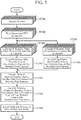
- FIG. 5 is a flowchart illustrating processing of the dielectric boundary surface estimating unit 500.
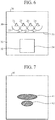
- FIG. 6 is a view illustrating a situation when wave data stored in the wave data storing unit 200 is obtained by observation.
- an operation example of the dielectric boundary surface estimation device 100 is described using the wave data obtained by observation in the situation illustrated in FIG. 6 .
- the dielectric to be observed is a space 31 having a dielectric constant of ⁇ r,1 .
- a space 32 having a relatively low dielectric constant of ⁇ r,2 ( ⁇ r,2 ⁇ ⁇ r,1 ) is included.
- Transceivers 21 to 24 of a radar device are arranged in a space 30 having a dielectric constant of ⁇ r,0 ( ⁇ r,0 ⁇ ⁇ r,1 ) lower than the dielectric constant ⁇ r,1 of the space 31.
- the transceivers 21 to 24 transmit pulse-shaped radio waves 25 to 28 toward the space 31.
- the transmitted radio waves 25 to 28 are scattered on a dielectric boundary surface 33 which is a boundary between the spaces 30 and 31 having different dielectric constants and on a dielectric boundary surface 34 which is a boundary between the spaces 31 and 32 having different dielectric constants.
- the transceivers 21 to 24 receive the radio waves 25 to 28 scattered on the dielectric boundary surfaces 33 and 34.
- the radar device converts scattering information of the radio waves from the dielectric boundary surfaces 33 and 34 into three-dimensional voxel data on the basis of transmission/reception results of the radio waves 25 to 28 and outputs the voxel data to the dielectric boundary surface estimation device 100.
- the above observation may be performed by a plurality of transceivers 21 to 24, or may be performed by moving one transceiver to the respective positions shown as the positions of the transceivers 21 to 24.
- wave data s(x, y, t) scattering information obtained by observing an inside of the dielectric by the radar device.
- xE[-L x /2, L x /2] is defined as the azimuth direction
- yE[-L y /2, L y /2] is defined as the elevation direction
- tE[0, T PRI ] is defined as the slant range direction.
- L x represents an aperture length in the azimuth direction
- L y represents an aperture length in the elevation direction
- T PRI represents a pulse repetition cycle.
- the wave data storing unit 200 receives and stores wave data obtained by observing the inside of the dielectric by the radar device.
- the wave data stored in the wave data storing unit 200 is transferred to the pre-processing unit 300.
- the pre-processing unit 300 performs the pre-processing at steps ST301 to ST303 to be described below in detail on the wave data transferred from the wave data storing unit 200 and outputs the processed wave data to the three-dimensional synthetic aperture processing unit 400.
- the pre-processing unit 300 removes the DC component in the range direction from the wave data. Specifically, the pre-processing unit 300 estimates a range direction DC component s 0,t (x, y, t) in consideration of a case where the wave data s(x, y, t) transferred from the wave data storing unit 200 is fixed decimal data and the like in accordance with equation (1). Subsequently, the pre-processing unit 300 obtains wave data s DC,t (x, y, t) from which the range direction DC component is removed by removing the range direction DC component s 0,t (x, y, t) from the wave data s(x, y, t) using equation (2).
- the pre-processing unit 300 removes the DC component in the azimuth direction from the wave data. Specifically, the pre-processing unit 300 estimates the azimuth direction DC component s 0,t,x (x, y, t) in consideration of a case where the wave data s(x, y, t) transferred from the wave data storing unit 200 is fixed decimal data and the like in accordance with equation (3).
- the pre-processing unit 300 obtains wave data s DC,t,x (x, y, t) from which the DC components in the azimuth direction and the range direction are removed by removing the azimuth direction DC component s 0,t,x (x, y, t) from the wave data s DC,t (x, y, t) from which the range direction DC component is removed using equation (4).
- the pre-processing unit 300 corrects attenuation of the wave when the radio wave passes through the inside of the dielectric by performing contrast correction on the wave data. Specifically, the pre-processing unit 300 defines a contrast correction function s CNT,t,x (x, y, t) in consideration of the attenuation of the wave as shown in equation (5) for the wave data s DC,t,x (x, y, t) in which the DC components in the azimuth direction and the range direction are removed.
- the pre-processing unit 300 performs the contrast correction on the wave data s DC,t,x (x, y, t) using equation (6) and obtains wave data s PRE (x, y, t) after the contrast correction.
- the pre-processing unit 300 outputs the pre-processed wave data s PRE (x, y, t) to the three-dimensional synthetic aperture processing unit 400.
- the three-dimensional synthetic aperture processing unit 400 performs three-dimensional synthetic aperture processing at steps ST401 to ST403 to be described in detail below on the pre-processed wave data output by the pre-processing unit 300 and outputs the wave data after the processing to the dielectric boundary surface estimating unit 500.
- the three-dimensional synthetic aperture processing unit 400 performs three-dimensional Fourier transform for converting the pre-processed wave data into wave data in a frequency space. Specifically, the three-dimensional synthetic aperture processing unit 400 performs three-dimensional fast Fourier transform (FFT) on the pre-processed wave data s PRE (x, y, t) received from the pre-processing unit 300 using equation (7) and converts the pre-processed wave data s PRE (x, y, t) into wave data S PRE (k x , k y , k) in the frequency space.
- FFT fast Fourier transform
- the three-dimensional synthetic aperture processing unit 400 performs azimuth bulk compression to compensate a wave surface of the wave data to a spherical shape in the frequency space. Specifically, the three-dimensional synthetic aperture processing unit 400 obtains wave data S BULK (k x , k y , k) in which the wave surface of the wave data S PRE (k x , k y , k) is made uniform and the image of the wave data is focused by performs the azimuth bulk compression by calculating equation (8) on the wave data S PRE (k x , k y , k) after the three-dimensional FFT and.
- S BULK k x k y k S PRE k x k y k ⁇ exp jR 0 k z
- Ro represents a focus distance, and is defined by, for example, equation (9-1).
- k z represents a wave number defined by equation (9-2).
- R 0 ⁇ r ,1 c T PRI / 2
- k z 4 k 2 ⁇ k x 2 ⁇ k y 2 2
- k k x 2 + k y 2 + k z 2
- the three-dimensional synthetic aperture processing unit 400 performs Stolt interpolation to orthogonalize a wave transmitting direction 2k of the wave data in the x axis and the y axis.
- the direction of a wave number vector means the wave surface and the wave transmitting direction, and the wave number vector 2k generally observed by the radar device can be orthogonally decomposed into the wave number vectors (k x , k y , k z ), for example. This means that equation (9-3) described above holds from the Pythagorean theorem.
- Equation (9-2) Although the wave number vectors k z and k y can be immediately defined to be orthogonal to each other on an antenna surface, k z in equation (9-2) described above cannot be observed directly and can be observed only as a function of (k x , k y , 2k). Processing of interpolation using equation (9-2) described above from (k x , k y , 2k) to (k x , k y , k z ) to make a state in which the observable and definable wave numbers (k x , k y , 2k) are orthogonal is the Stolt interpolation processing.
- the three-dimensional synthetic aperture processing unit 400 obtains wave data S SAR (k x , k y , k z ) after the three-dimensional synthetic aperture processing by performing the Stolt interpolation to convert the wave number space (k x , k y , k) to (k x , k y , k z ) for the wave data S BULK (k x , k y , k) after the azimuth bulk compression.
- the three-dimensional synthetic aperture processing unit 400 outputs the wave data S SAR (k x , k y , k z ) after the three-dimensional synthetic aperture processing to the dielectric boundary surface estimating unit 500.
- FIG. 7 is a view illustrating wave data 40 after the three-dimensional synthetic aperture processing is performed by the three-dimensional synthetic aperture processing unit 400, that is, the wave data S SAR (k x , k y , k z ).
- the high-dielectric constant side boundary 41 in the wave data 40 after the three-dimensional synthetic aperture processing corresponds to the dielectric boundary surface 33 in the observation system 20 illustrated in FIG. 6 .
- the low-dielectric constant side boundary 42 in the wave data 40 after the three-dimensional synthetic aperture processing corresponds to the dielectric boundary surface 34 in the observation system 20 illustrated in FIG. 6 .
- the three-dimensional synthetic aperture processing performed by the three-dimensional synthetic aperture processing unit 400 is a technology well-known as the Omega-K system.
- the dielectric boundary surface estimating unit 500 calculates the width and the thickness of the dielectric boundary surface by performing dielectric boundary surface estimation processing at steps ST501 to ST509 to be described below in detail on the wave data after the three-dimensional synthetic aperture processing output by the three-dimensional synthetic aperture processing unit 400, and outputs the calculation result to the output data storing unit 600.
- the dielectric boundary surface estimating unit 500 decomposes the dielectric boundary surface into a dielectric boundary point group by dividing the wave data after the three-dimensional synthetic aperture processing into a plurality of observation units from respective phase centers.
- a process at step ST501 is referred to as aperture division.
- the dielectric boundary surface estimating unit 500 obtains wave data per aperture S SAR,n,m (k x , k y , k z ) after aperture division by dividing the wave data S SAR (k x , k y , k z ) after the three-dimensional synthetic aperture processing received from the three-dimensional synthetic aperture processing unit 400 by N in the azimuth direction and by M in the elevation direction using equation (10).
- K Bcut,x represents an effective bandwidth in the azimuth direction after the aperture division
- K Bcut,y represents an effective bandwidth in the elevation direction after the aperture division.
- ⁇ k x represents a pitch width of the aperture division in the azimuth direction
- ⁇ k y represents a pitch width of the aperture division in the elevation direction.
- K B,x and K B,y When the bandwidths after the aperture division are represented by K B,x and K B,y , the relationship in equation (11) is satisfied among K B,x , K B,y , K Bcut,x , and K Bcut,y .
- the dielectric boundary surface estimating unit 500 performs three-dimensional inverse Fourier transform which converts the wave data per aperture obtained by the aperture division from a frequency domain to a spatial domain. Specifically, the dielectric boundary surface estimating unit 500 performs three-dimensional inverse fast Fourier transform (IFFT) on the wave data per aperture S SAR,n,m (k x , k y , k z ) using equation (12) and converts it into wave data per aperture I SAR,n,m (x, y, z) of the spatial domain.
- IFFT three-dimensional inverse fast Fourier transform
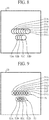
- FIG. 8 is a view illustrating wave data 50 after the dielectric boundary surface estimating unit 500 performs the aperture division and the three-dimensional IFFF.
- a portion of the high-dielectric constant side boundary 41 in the wave data 40 after the three-dimensional synthetic aperture processing illustrated in FIG. 7 is divided into a plurality of local small areas as shown in wave data per aperture 51A to 51G illustrated in FIG. 8 .
- the wave data per aperture 51A to 51G can be referred to as the dielectric boundary point group obtained by decomposing the dielectric boundary surface 33.
- the wave data per aperture 52A to 52D can be referred to as the dielectric boundary point group obtained by decomposing the dielectric boundary surface 34.
- a portion other than the wave data per aperture 51A to 51G and 52A to 52D in the wave data 50 is also divided into a plurality of local small areas as is the case with the wave data per aperture 51A to 51G and 52A to 52D.
- the dielectric boundary surface estimating unit 500 extracts high-dielectric constant side boundary points exceeding a predetermined threshold from the wave data per aperture.
- the dielectric boundary surface estimating unit 500 records the extracted high-dielectric constant side boundary point group as a high-dielectric constant side boundary point trajectory.
- the dielectric boundary surface estimating unit 500 obtains a set of local maximum points of the wave data per aperture exceeding a threshold T, that is, a high-dielectric constant side boundary point trajectory (X top,n,m , Y top,n,m , Z top,n,m ) by calculating equation (13) for high-dielectric constant side boundary surface candidates ⁇ x + , y +
- T represents a predetermined threshold, which is a value corresponding to signal power of the radio wave scattered on the dielectric boundary surface 33 on the high-dielectric constant side.
- the dielectric boundary surface estimating unit 500 extracts low-dielectric constant side boundary points smaller than the predetermined threshold from the wave data per aperture.
- the dielectric boundary surface estimating unit 500 records the extracted low-dielectric constant side boundary point group as a low-dielectric constant side boundary point trajectory.
- the dielectric boundary surface estimating unit 500 obtains a set of local minimum points of the wave data per aperture smaller than the threshold T, that is, a low-dielectric constant side boundary point trajectory (x btm,n,m , y btm,n,m , z btm,n,m ) by calculating equation (14) for low-dielectric constant side boundary surface candidates ⁇ x - , y -
- x btm , n , m y btm , n , m z btm , n , m arg min x ⁇ , y ⁇ , z Re I SAR , n , m x ⁇ y ⁇ z
- FIG. 9 is a view illustrating a high-dielectric constant side boundary point trajectory 51 and a low-dielectric constant side boundary point trajectory 52 calculated by the dielectric boundary surface estimating unit 500.
- the high-dielectric constant side boundary point trajectory 51 is a set of local maximum points of the wave data per aperture 51A to 51G on the high-dielectric constant side exceeding the threshold.
- the low-dielectric constant side boundary point trajectory 52 is a set of local minimum points of the wave data per aperture 52A to 52D on the low-dielectric constant side smaller than the threshold.
- the local maximum points of the wave data per aperture 51A to 51G and the local minimum points of the wave data per aperture 52A to 52D are indicated by the intersection of each of "x" marks.
- the dielectric boundary surface estimating unit 500 calculates the width of the dielectric boundary surface using the obtained high-dielectric constant side boundary point trajectory 51. Specifically, the dielectric boundary surface estimating unit 500 calculates the widths ( ⁇ x, ⁇ y) of the dielectric boundary surface from the high-dielectric constant side boundary point trajectory 51 using equations (15) and (16).
- the dielectric boundary surface estimating unit 500 calculates a thickness of a space between the dielectric boundary surfaces using the obtained high-dielectric constant side boundary point trajectory 51 and low-dielectric constant side boundary trajectory 52. Specifically, the dielectric boundary surface estimating unit 500 calculates the distance from the center of the high-dielectric constant side boundary point trajectory 51 to the center of the low-dielectric constant side boundary point trajectory 52 using equation (17) as a thickness ⁇ z between the dielectric boundary surfaces.
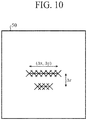
- FIG. 10 is a view illustrating the widths ( ⁇ x, ⁇ y) and the thickness ⁇ z of the dielectric boundary surface calculated by the dielectric boundary surface estimating unit 500.
- the widths ( ⁇ x, ⁇ y) of the dielectric boundary surface indicated by an arrow in FIG. 10 correspond to widths of the dielectric boundary surface 34 being the boundary between the space 31 which is the dielectric to be observed and the space 32 included in the space 31 in FIG. 6 .
- the thickness ⁇ z between the dielectric boundary surfaces indicated by an arrow in FIG. 10 corresponds to a thickness of the space 31 from the dielectric boundary surface 33 to the dielectric boundary surface 34 in FIG. 6 .
- the dielectric boundary surface estimating unit 500 records a calculation result of the widths and the thickness of the dielectric boundary surface. In addition, the dielectric boundary surface estimating unit 500 transfers the recorded calculation result to the output data storing unit 600.
- the output data storing unit 600 receives the calculation result of the widths and the thickness of the dielectric boundary surface transferred from the dielectric boundary surface estimating unit 500 and the wave data after the three-dimensional synthetic aperture processing and stores them.
- the output data storing unit 600 can output the stored calculation result and wave data to the outside.
- the output data storing unit 600 may receive the wave data S SAR (k x , k y , k z ) after the three-dimensional synthetic aperture processing directly from the three-dimensional synthetic aperture processing unit 400 or via the dielectric boundary surface estimating unit 500.
- a dielectric boundary surface estimation device 100 includes: a pre-processing unit 300 pre-processing wave data obtained by observing a dielectric by a radar device; a three-dimensional synthetic aperture processing unit 400 performing three-dimensional synthetic aperture processing on the wave data pre-processed by the pre-processing unit 300; and a dielectric boundary surface estimating unit 500 estimating a boundary surface between areas having different dielectric constants to each other using the wave data on which the three-dimensional synthetic aperture processing is performed by the three-dimensional synthetic aperture processing unit 400 and calculating a width and a thickness of the boundary surface. Since the position of the dielectric boundary surface is estimated using the wave data subjected to the three-dimensional synthetic aperture processing, it is possible to estimate the widths and the thickness of the dielectric boundary surface with high accuracy.
- the dielectric boundary surface estimating unit 500 performs division of the wave data on which the three-dimensional synthetic aperture processing unit 400 performs the three-dimensional synthetic aperture processing in an azimuth direction and an elevation direction, performs three-dimensional inverse Fourier transform on the wave data after the division, extracts a low-dielectric constant side boundary point trajectory 52 corresponding to a dielectric boundary surface 34 on the low-dielectric constant side and a high-dielectric constant side boundary point trajectory 51 corresponding to a dielectric boundary surface 33 on the high-dielectric constant side out of the wave data after the division subjected to the three-dimensional inverse Fourier transform, calculates a width of the dielectric boundary surface 34 on the low-dielectric constant side from the high-dielectric constant side boundary point trajectory 51, and calculates a thickness from the dielectric boundary surface 33 on the high-dielectric constant side to the dielectric boundary surface 34 on the low-dielectric constant side on a basis of a distance between a center of the high-dielectric constant
- the dielectric boundary surface estimation device 100 may also be used when the dielectric constant of the space 32 is higher than the dielectric constant of the space 31.
- the dielectric boundary surface estimation device 100 can calculate the widths and the thickness of the dielectric boundary surface by performing the processing illustrated in FIGS. 3 to 5 .
- “high-dielectric constant side” is replaced with “low-dielectric constant side”
- “low-dielectric constant side” is replaced with “high-dielectric constant side”
- "local maximum point” is replaced with "local minimum point”
- "local minimum point” is replaced with "local maximum point”.
- the dielectric boundary surface estimating unit 500 uses the set of the local minimum points of the wave data per aperture which are smaller than the threshold, that is, the low-dielectric constant side boundary point trajectory.
- the three-dimensional synthetic aperture processing unit 400 performs three-dimensional Fourier transform on the wave data pre-processed by the pre-processing unit 300, performs azimuth bulk compression to make a wave surface uniform on the wave data subjected to the three-dimensional Fourier transform, and thereafter performs interpolation to orthogonalize a wave transmitting direction.
- the position estimation accuracy of the dielectric boundary surface can be further improved.
- the pre-processing unit 300 removes a DC component in a range direction and a DC component in an azimuth direction from the wave data obtained by observing the dielectric by the radar device, and corrects attenuation of the wave when passing through the dielectric. It is possible to further improve the position estimation accuracy of the dielectric boundary surface by removing the DC component of the wave data and correcting contrast.
- any component of the embodiment may be modified, or any component of the embodiment may be omitted without departing from the scope of the invention.
- the dielectric boundary surface estimation device 100 is provided with the wave data storing unit 200 and the output data storing unit 600, but the wave data storing unit 200 and the output data storing unit 600 are not necessarily required. That is, the dielectric boundary surface estimation device 100 may have any configuration as long as it can receive wave data from the outside, calculate the widths and the thickness of a dielectric boundary surface, and output the calculation result to the outside.
- the dielectric boundary surface estimation device calculates the widths and the thickness of a dielectric boundary surface using the wave data subjected to the three-dimensional synthetic aperture processing, so that it is suitable for a dielectric boundary surface estimation device used for detecting cancer, diagnosing material deterioration of a construction and the like.
- 11 Storage device for input
- 12 Processor
- 13 Memory
- 14 Storage device for output
- 20 Observation system
- 21 to 24 Transceiver
- 25 to 28 Radio wave
- 30 to 32 Space
- 33, 34 Dielectric boundary surface
- 40, 50 Wave data
- 52 Low-dielectric constant side boundary point trajectory
- 51A to 51G, 52A to 52D Wave data per aperture
- 100 Dielectric boundary surface estimation device
- 200 Wave data storing unit
- 300 Pre-processing unit
- 400 Three-dimensional synthetic aperture processing unit
- 500 Dielectric boundary surface estimating unit
- 600 Output data storing unit.
Landscapes
- Engineering & Computer Science (AREA)
- Remote Sensing (AREA)
- Radar, Positioning & Navigation (AREA)
- Physics & Mathematics (AREA)
- Electromagnetism (AREA)
- General Physics & Mathematics (AREA)
- Computer Networks & Wireless Communication (AREA)
- Artificial Intelligence (AREA)
- Life Sciences & Earth Sciences (AREA)
- Computer Vision & Pattern Recognition (AREA)
- Environmental & Geological Engineering (AREA)
- Geology (AREA)
- General Life Sciences & Earth Sciences (AREA)
- Geophysics (AREA)
- Signal Processing (AREA)
- Radar Systems Or Details Thereof (AREA)
Abstract
Description
- The present invention relates to a dielectric boundary surface estimation device for estimating a boundary surface between dielectrics having different dielectric constants using a radio wave.
- A dielectric boundary surface estimation device is used for measuring a state in a dielectric utilizing a property of passing through an inside of the dielectric which is a property of a radio wave as a wave, and contributes to cancer detection and diagnosis of material deterioration of a construction.
- In the cavity thickness investigating method disclosed in following Patent Literature 1, scattering from a dielectric boundary point is observed with S transform processing. In this method, not a boundary surface but only a boundary point of a dielectric is measured. As for measurement of the shape of a dielectric, an ellipsoid is simply applied on a basis of visual observation irrespective of S transform and no special plan is devised.
- Patent Literature 1:
JP 2015-197398 A - In the cavity thickness investigating method disclosed in Patent Literature 1 described above, there is a problem that only presence of a boundary point which is a part of a dielectric boundary surface can be grasped, and it is not possible to grasp the boundary surface. In addition, in Patent Literature 1 described above, as a method of estimating the shape of a dielectric, a method of applying an ellipsoid in an environment in which synthetic aperture processing is not applied is adopted, so that the width of a dielectric boundary surface in the horizontal direction cannot be accurately estimated.
- The present invention has been made to solve the above-described problem and an object thereof is to accurately estimate a width and a thickness of a dielectric boundary surface.
- A dielectric boundary surface estimation device according to the present invention includes: a pre-processing unit pre-processing wave data obtained by observing a dielectric by a radar device; a three-dimensional synthetic aperture processing unit performing three-dimensional synthetic aperture processing on the wave data pre-processed by the pre-processing unit; and a dielectric boundary surface estimating unit estimating a boundary surface between areas having different dielectric constants to each other using the wave data on which the three-dimensional synthetic aperture processing is performed by the three-dimensional synthetic aperture processing unit and calculating a width and a thickness of the boundary surface.
- According to the present invention, since a dielectric boundary surface is estimated using wave data subjected to three-dimensional synthetic aperture processing, it is possible to accurately estimate a width and a thickness of a dielectric boundary surface.
-
-
FIG. 1 is a functional configuration diagram illustrating a configuration example of a dielectric boundary surface estimation device according to a first embodiment of the present invention;-
FIG. 2 is a hardware configuration diagram illustrating a configuration example of the dielectric boundary surface estimation device according to the first embodiment of the present invention; -
FIG. 3 is a flowchart illustrating processing performed by a pre-processing unit of the dielectric boundary surface estimation device according to the first embodiment of the present invention; -
FIG. 4 is a flowchart illustrating processing performed by a three-dimensional synthetic aperture processing unit of the dielectric boundary surface estimation device according to the first embodiment of the present invention; -
FIG. 5 is a flowchart illustrating processing performed by a dielectric boundary surface estimating unit of the dielectric boundary surface estimation device according to the first embodiment of the present invention; -
FIG. 6 is a view illustrating a situation when wave data stored in a wave data storing unit of the dielectric boundary surface estimation device according to the first embodiment of the present invention is observed; -
FIG. 7 is a view illustrating the wave data after the three-dimensional synthetic aperture processing unit of the dielectric boundary surface estimation device according to the first embodiment of the present invention performed three-dimensional synthetic aperture processing; -
FIG. 8 is a view illustrating the wave data after the dielectric boundary surface estimating unit of the dielectric boundary surface estimation device according to the first embodiment of the present invention performed aperture division and three-dimensional inverse fast Fourier transform; -
FIG. 9 is a view illustrating a high-dielectric constant side boundary point trajectory and a low-floating constant side boundary point trajectory calculated by the dielectric boundary surface estimating unit of the dielectric boundary surface estimation device according to the first embodiment of the present invention; and -
FIG. 10 is a view illustrating widths and a thickness of a dielectric boundary surface calculated by the dielectric boundary surface estimating unit of the dielectric boundary surface estimation device according to the first embodiment of the present invention.
-
- Hereinafter, in order to describe the present invention in more detail, some embodiments for carrying out the present invention will be described with reference to the accompanying drawings.
-
FIG. 1 is a functional configuration diagram illustrating a configuration example of a dielectric boundarysurface estimation device 100 according to a first embodiment of the present invention. As illustrated in the drawing, the dielectric boundarysurface estimation device 100 includes a wavedata storing unit 200, apre-processing unit 300, a three-dimensional syntheticaperture processing unit 400, a dielectric boundarysurface estimating unit 500, and an outputdata storing unit 600. -
FIG. 2 is a hardware configuration diagram illustrating a configuration example of the dielectric boundarysurface estimation device 100 according to the first embodiment of the present invention. The wavedata storing unit 200 in the dielectric boundarysurface estimation device 100 is a storage device forinput 11 and the outputdata storing unit 600 is a storage device foroutput 14. The storage device forinput 11, the storage device foroutput 14, and amemory 13 to be described later may be a nonvolatile or volatile semiconductor device memory such as a random access memory (RAM), a read only memory (ROM), an erasable programmable ROM (EPROM), a flash memory, and a solid state drive (SSD), or a magnetic storage medium such as a hard disk and a flexible disk. - The functions of the
pre-processing unit 300, the three-dimensional syntheticaperture processing unit 400, and the dielectric boundarysurface estimating unit 500 in the dielectric boundarysurface estimation device 100 are implemented by a processing circuit. That is, the dielectric boundarysurface estimation device 100 is provided with the processing circuit for reading wave data stored in the storage device forinput 11, pre-processing the wave data, performing three-dimensional synthetic aperture processing on the pre-processed wave data, estimating a boundary surface of the dielectric using the wave data subjected to the three-dimensional synthetic aperture processing, calculating a width and a thickness of the boundary surface, and storing the calculation result in the storage device foroutput 14. The processing circuit is aprocessor 12 which executes a program stored in thememory 13. Theprocessor 12 is also referred to as a central processing unit (CPU), an arithmetic device, a microprocessor, a microcomputer or the like. - The functions of the
pre-processing unit 300, the three-dimensional syntheticaperture processing unit 400, and the dielectric boundarysurface estimating unit 500 are implemented by software, firmware, or a combination of software and firmware. The software or firmware is described as a program and stored in thememory 13. Theprocessor 12 implements the functions of the respective units by reading and executing the program stored in thememory 13. That is, the dielectric boundarysurface estimation device 100 includes thememory 13 for storing the program which is executed by theprocessor 12 to eventually execute steps illustrated inFIGS. 3 to 5 to be described later. It may also be said that the program allows a computer to execute a procedure or a method of each of thepre-processing unit 300, the three-dimensional syntheticaperture processing unit 400, and the dielectric boundarysurface estimating unit 500. - Next, operation of the dielectric boundary
surface estimation device 100 according to the first embodiment of the present invention will be described. -
FIG. 3 is a flowchart illustrating processing of thepre-processing unit 300.FIG. 4 is a flowchart illustrating processing of the three-dimensional syntheticaperture processing unit 400.FIG. 5 is a flowchart illustrating processing of the dielectric boundarysurface estimating unit 500. -
FIG. 6 is a view illustrating a situation when wave data stored in the wavedata storing unit 200 is obtained by observation. Hereinafter, an operation example of the dielectric boundarysurface estimation device 100 is described using the wave data obtained by observation in the situation illustrated inFIG. 6 . - In an
observation system 20 inFIG. 6 , the dielectric to be observed is aspace 31 having a dielectric constant of εr,1. In thespace 31, aspace 32 having a relatively low dielectric constant of εr,2 (εr,2 < εr,1) is included.Transceivers 21 to 24 of a radar device are arranged in aspace 30 having a dielectric constant of εr,0 (εr,0 < εr,1) lower than the dielectric constant εr,1 of thespace 31. - The
transceivers 21 to 24 transmit pulse-shaped radio waves 25 to 28 toward thespace 31. The transmittedradio waves 25 to 28 are scattered on adielectric boundary surface 33 which is a boundary between thespaces dielectric boundary surface 34 which is a boundary between thespaces transceivers 21 to 24 receive theradio waves 25 to 28 scattered on thedielectric boundary surfaces dielectric boundary surfaces radio waves 25 to 28 and outputs the voxel data to the dielectric boundarysurface estimation device 100. - The above observation may be performed by a plurality of
transceivers 21 to 24, or may be performed by moving one transceiver to the respective positions shown as the positions of thetransceivers 21 to 24. - Hereinafter, scattering information obtained by observing an inside of the dielectric by the radar device is referred to as wave data s(x, y, t). Note that xE[-Lx/2, Lx/2] is defined as the azimuth direction, yE[-Ly/2, Ly/2] is defined as the elevation direction, and tE[0, TPRI] is defined as the slant range direction. Lx represents an aperture length in the azimuth direction, Ly represents an aperture length in the elevation direction, and TPRI represents a pulse repetition cycle.
- The wave
data storing unit 200 receives and stores wave data obtained by observing the inside of the dielectric by the radar device. The wave data stored in the wavedata storing unit 200 is transferred to thepre-processing unit 300. - The
pre-processing unit 300 performs the pre-processing at steps ST301 to ST303 to be described below in detail on the wave data transferred from the wavedata storing unit 200 and outputs the processed wave data to the three-dimensional syntheticaperture processing unit 400. - At step ST301, the
pre-processing unit 300 removes the DC component in the range direction from the wave data. Specifically, thepre-processing unit 300 estimates a range direction DC component s0,t(x, y, t) in consideration of a case where the wave data s(x, y, t) transferred from the wavedata storing unit 200 is fixed decimal data and the like in accordance with equation (1). Subsequently, thepre-processing unit 300 obtains wave data sDC,t(x, y, t) from which the range direction DC component is removed by removing the range direction DC component s0,t(x, y, t) from the wave data s(x, y, t) using equation (2).

- At step ST302, the
pre-processing unit 300 removes the DC component in the azimuth direction from the wave data. Specifically, thepre-processing unit 300 estimates the azimuth direction DC component s0,t,x(x, y, t) in consideration of a case where the wave data s(x, y, t) transferred from the wavedata storing unit 200 is fixed decimal data and the like in accordance with equation (3). Subsequently, thepre-processing unit 300 obtains wave data sDC,t,x(x, y, t) from which the DC components in the azimuth direction and the range direction are removed by removing the azimuth direction DC component s0,t,x(x, y, t) from the wave data sDC,t(x, y, t) from which the range direction DC component is removed using equation (4).

- At step ST303, the
pre-processing unit 300 corrects attenuation of the wave when the radio wave passes through the inside of the dielectric by performing contrast correction on the wave data. Specifically, thepre-processing unit 300 defines a contrast correction function sCNT,t,x(x, y, t) in consideration of the attenuation of the wave as shown in equation (5) for the wave data sDC,t,x(x, y, t) in which the DC components in the azimuth direction and the range direction are removed. Subsequently, thepre-processing unit 300 performs the contrast correction on the wave data sDC,t,x(x, y, t) using equation (6) and obtains wave data sPRE(x, y, t) after the contrast correction. Thepre-processing unit 300 outputs the pre-processed wave data sPRE(x, y, t) to the three-dimensional syntheticaperture processing unit 400.

- The three-dimensional synthetic
aperture processing unit 400 performs three-dimensional synthetic aperture processing at steps ST401 to ST403 to be described in detail below on the pre-processed wave data output by thepre-processing unit 300 and outputs the wave data after the processing to the dielectric boundarysurface estimating unit 500. - At step ST401, the three-dimensional synthetic
aperture processing unit 400 performs three-dimensional Fourier transform for converting the pre-processed wave data into wave data in a frequency space. Specifically, the three-dimensional syntheticaperture processing unit 400 performs three-dimensional fast Fourier transform (FFT) on the pre-processed wave data sPRE(x, y, t) received from thepre-processing unit 300 using equation (7) and converts the pre-processed wave data sPRE(x, y, t) into wave data SPRE(kx, ky, k) in the frequency space.
- At step ST402, the three-dimensional synthetic
aperture processing unit 400 performs azimuth bulk compression to compensate a wave surface of the wave data to a spherical shape in the frequency space. Specifically, the three-dimensional syntheticaperture processing unit 400 obtains wave data SBULK(kx, ky, k) in which the wave surface of the wave data SPRE(kx, ky, k) is made uniform and the image of the wave data is focused by performs the azimuth bulk compression by calculating equation (8) on the wave data SPRE(kx, ky, k) after the three-dimensional FFT and.
- Note that, in equation (8), Ro represents a focus distance, and is defined by, for example, equation (9-1). kz represents a wave number defined by equation (9-2).


- At step ST403, the three-dimensional synthetic
aperture processing unit 400 performs Stolt interpolation to orthogonalize a wave transmitting direction 2k of the wave data in the x axis and the y axis. The direction of a wave number vector means the wave surface and the wave transmitting direction, and the wave number vector 2k generally observed by the radar device can be orthogonally decomposed into the wave number vectors (kx, ky, kz), for example. This means that equation (9-3) described above holds from the Pythagorean theorem. Although the wave number vectors kz and ky can be immediately defined to be orthogonal to each other on an antenna surface, kz in equation (9-2) described above cannot be observed directly and can be observed only as a function of (kx, ky, 2k). Processing of interpolation using equation (9-2) described above from (kx, ky, 2k) to (kx, ky, kz) to make a state in which the observable and definable wave numbers (kx, ky, 2k) are orthogonal is the Stolt interpolation processing. Specifically, the three-dimensional syntheticaperture processing unit 400 obtains wave data SSAR(kx, ky, kz) after the three-dimensional synthetic aperture processing by performing the Stolt interpolation to convert the wave number space (kx, ky, k) to (kx, ky, kz) for the wave data SBULK(kx, ky, k) after the azimuth bulk compression. The three-dimensional syntheticaperture processing unit 400 outputs the wave data SSAR(kx, ky, kz) after the three-dimensional synthetic aperture processing to the dielectric boundarysurface estimating unit 500. -
FIG. 7 is a view illustratingwave data 40 after the three-dimensional synthetic aperture processing is performed by the three-dimensional syntheticaperture processing unit 400, that is, the wave data SSAR(kx, ky, kz). The high-dielectricconstant side boundary 41 in thewave data 40 after the three-dimensional synthetic aperture processing corresponds to thedielectric boundary surface 33 in theobservation system 20 illustrated inFIG. 6 . The low-dielectricconstant side boundary 42 in thewave data 40 after the three-dimensional synthetic aperture processing corresponds to thedielectric boundary surface 34 in theobservation system 20 illustrated inFIG. 6 . - Note that the three-dimensional synthetic aperture processing performed by the three-dimensional synthetic
aperture processing unit 400 is a technology well-known as the Omega-K system. - In addition, as an interpolation method performed at step 403, other than the Stolt interpolation described above as an example, sinc interpolation or cubic interpolation may be used, for example.
- The dielectric boundary
surface estimating unit 500 calculates the width and the thickness of the dielectric boundary surface by performing dielectric boundary surface estimation processing at steps ST501 to ST509 to be described below in detail on the wave data after the three-dimensional synthetic aperture processing output by the three-dimensional syntheticaperture processing unit 400, and outputs the calculation result to the outputdata storing unit 600. - At step ST501, the dielectric boundary
surface estimating unit 500 decomposes the dielectric boundary surface into a dielectric boundary point group by dividing the wave data after the three-dimensional synthetic aperture processing into a plurality of observation units from respective phase centers. Hereinafter, a process at step ST501 is referred to as aperture division. Specifically, the dielectric boundarysurface estimating unit 500 obtains wave data per aperture SSAR,n,m(kx, ky, kz) after aperture division by dividing the wave data SSAR(kx, ky, kz) after the three-dimensional synthetic aperture processing received from the three-dimensional syntheticaperture processing unit 400 by N in the azimuth direction and by M in the elevation direction using equation (10).
- Note that, in equation (10), KBcut,x represents an effective bandwidth in the azimuth direction after the aperture division, and KBcut,y represents an effective bandwidth in the elevation direction after the aperture division. Further, nE[0,N-1] and mE[0,M-1]. Δkx represents a pitch width of the aperture division in the azimuth direction and Δky represents a pitch width of the aperture division in the elevation direction.
- When the bandwidths after the aperture division are represented by KB,x and KB,y, the relationship in equation (11) is satisfied among KB,x, KB,y, KBcut,x, and KBcut,y.

- At step ST502, the dielectric boundary
surface estimating unit 500 performs three-dimensional inverse Fourier transform which converts the wave data per aperture obtained by the aperture division from a frequency domain to a spatial domain. Specifically, the dielectric boundarysurface estimating unit 500 performs three-dimensional inverse fast Fourier transform (IFFT) on the wave data per aperture SSAR,n,m(kx, ky, kz) using equation (12) and converts it into wave data per aperture ISAR,n,m(x, y, z) of the spatial domain.
-
FIG. 8 is a view illustratingwave data 50 after the dielectric boundarysurface estimating unit 500 performs the aperture division and the three-dimensional IFFF. By the processes at steps ST501 and ST502, a portion of the high-dielectricconstant side boundary 41 in thewave data 40 after the three-dimensional synthetic aperture processing illustrated inFIG. 7 is divided into a plurality of local small areas as shown in wave data peraperture 51A to 51G illustrated inFIG. 8 . The wave data peraperture 51A to 51G can be referred to as the dielectric boundary point group obtained by decomposing thedielectric boundary surface 33. Similarly, a portion of the low-dielectricconstant side boundary 42 in thewave data 40 after the three-dimensional synthetic aperture processing illustrated inFIG. 7 is divided into a plurality of local small areas as shown in wave data peraperture 52A to 52D illustrated inFIG. 8 . The wave data peraperture 52A to 52D can be referred to as the dielectric boundary point group obtained by decomposing thedielectric boundary surface 34. - Note that, although not illustrated in
FIG. 8 , a portion other than the wave data peraperture 51A to 51G and 52A to 52D in thewave data 50 is also divided into a plurality of local small areas as is the case with the wave data peraperture 51A to 51G and 52A to 52D. - At step ST503, the dielectric boundary
surface estimating unit 500 extracts high-dielectric constant side boundary points exceeding a predetermined threshold from the wave data per aperture. At subsequent step ST505, the dielectric boundarysurface estimating unit 500 records the extracted high-dielectric constant side boundary point group as a high-dielectric constant side boundary point trajectory. - Specifically, the dielectric boundary
surface estimating unit 500 obtains a set of local maximum points of the wave data per aperture exceeding a threshold T, that is, a high-dielectric constant side boundary point trajectory (Xtop,n,m, Ytop,n,m, Ztop,n,m) by calculating equation (13) for high-dielectric constant side boundary surface candidates {x+, y+ |Re[ISAR,n,m(x, y, z)] ≥ T} exceeding the threshold T out of the wave data per aperture. - Note that, in next equation (13) and equation (14) to be described below, T represents a predetermined threshold, which is a value corresponding to signal power of the radio wave scattered on the
dielectric boundary surface 33 on the high-dielectric constant side.
- At step ST504, the dielectric boundary
surface estimating unit 500 extracts low-dielectric constant side boundary points smaller than the predetermined threshold from the wave data per aperture. At subsequent step ST506, the dielectric boundarysurface estimating unit 500 records the extracted low-dielectric constant side boundary point group as a low-dielectric constant side boundary point trajectory. - Specifically, the dielectric boundary
surface estimating unit 500 obtains a set of local minimum points of the wave data per aperture smaller than the threshold T, that is, a low-dielectric constant side boundary point trajectory (xbtm,n,m, ybtm,n,m, zbtm,n,m) by calculating equation (14) for low-dielectric constant side boundary surface candidates {x-, y-|Re[ISAR,n,m(x, y, z)]<T} smaller than the threshold T out of the wave data per aperture.
-
FIG. 9 is a view illustrating a high-dielectric constant sideboundary point trajectory 51 and a low-dielectric constant sideboundary point trajectory 52 calculated by the dielectric boundarysurface estimating unit 500. The high-dielectric constant sideboundary point trajectory 51 is a set of local maximum points of the wave data peraperture 51A to 51G on the high-dielectric constant side exceeding the threshold. The low-dielectric constant sideboundary point trajectory 52 is a set of local minimum points of the wave data peraperture 52A to 52D on the low-dielectric constant side smaller than the threshold. - Note that, in
FIG. 9 , the local maximum points of the wave data peraperture 51A to 51G and the local minimum points of the wave data peraperture 52A to 52D are indicated by the intersection of each of "x" marks. - At step ST507, the dielectric boundary
surface estimating unit 500 calculates the width of the dielectric boundary surface using the obtained high-dielectric constant sideboundary point trajectory 51. Specifically, the dielectric boundarysurface estimating unit 500 calculates the widths (Δx, Δy) of the dielectric boundary surface from the high-dielectric constant sideboundary point trajectory 51 using equations (15) and (16).

- At step ST508, the dielectric boundary
surface estimating unit 500 calculates a thickness of a space between the dielectric boundary surfaces using the obtained high-dielectric constant sideboundary point trajectory 51 and low-dielectric constantside boundary trajectory 52. Specifically, the dielectric boundarysurface estimating unit 500 calculates the distance from the center of the high-dielectric constant sideboundary point trajectory 51 to the center of the low-dielectric constant sideboundary point trajectory 52 using equation (17) as a thickness Δz between the dielectric boundary surfaces.

-
FIG. 10 is a view illustrating the widths (Δx, Δy) and the thickness Δz of the dielectric boundary surface calculated by the dielectric boundarysurface estimating unit 500. The widths (Δx, Δy) of the dielectric boundary surface indicated by an arrow inFIG. 10 correspond to widths of thedielectric boundary surface 34 being the boundary between thespace 31 which is the dielectric to be observed and thespace 32 included in thespace 31 inFIG. 6 . The thickness Δz between the dielectric boundary surfaces indicated by an arrow inFIG. 10 corresponds to a thickness of thespace 31 from thedielectric boundary surface 33 to thedielectric boundary surface 34 inFIG. 6 . - At step ST509, the dielectric boundary
surface estimating unit 500 records a calculation result of the widths and the thickness of the dielectric boundary surface. In addition, the dielectric boundarysurface estimating unit 500 transfers the recorded calculation result to the outputdata storing unit 600. - The output
data storing unit 600 receives the calculation result of the widths and the thickness of the dielectric boundary surface transferred from the dielectric boundarysurface estimating unit 500 and the wave data after the three-dimensional synthetic aperture processing and stores them. The outputdata storing unit 600 can output the stored calculation result and wave data to the outside. - The output
data storing unit 600 may receive the wave data SSAR(kx, ky, kz) after the three-dimensional synthetic aperture processing directly from the three-dimensional syntheticaperture processing unit 400 or via the dielectric boundarysurface estimating unit 500. - As is apparent from above, according to the first embodiment, a dielectric boundary
surface estimation device 100 includes: apre-processing unit 300 pre-processing wave data obtained by observing a dielectric by a radar device; a three-dimensional syntheticaperture processing unit 400 performing three-dimensional synthetic aperture processing on the wave data pre-processed by thepre-processing unit 300; and a dielectric boundarysurface estimating unit 500 estimating a boundary surface between areas having different dielectric constants to each other using the wave data on which the three-dimensional synthetic aperture processing is performed by the three-dimensional syntheticaperture processing unit 400 and calculating a width and a thickness of the boundary surface. Since the position of the dielectric boundary surface is estimated using the wave data subjected to the three-dimensional synthetic aperture processing, it is possible to estimate the widths and the thickness of the dielectric boundary surface with high accuracy. - Further, according to the first embodiment, the dielectric boundary
surface estimating unit 500 performs division of the wave data on which the three-dimensional syntheticaperture processing unit 400 performs the three-dimensional synthetic aperture processing in an azimuth direction and an elevation direction, performs three-dimensional inverse Fourier transform on the wave data after the division, extracts a low-dielectric constant sideboundary point trajectory 52 corresponding to adielectric boundary surface 34 on the low-dielectric constant side and a high-dielectric constant sideboundary point trajectory 51 corresponding to adielectric boundary surface 33 on the high-dielectric constant side out of the wave data after the division subjected to the three-dimensional inverse Fourier transform, calculates a width of thedielectric boundary surface 34 on the low-dielectric constant side from the high-dielectric constant sideboundary point trajectory 51, and calculates a thickness from thedielectric boundary surface 33 on the high-dielectric constant side to thedielectric boundary surface 34 on the low-dielectric constant side on a basis of a distance between a center of the high-dielectric constant sideboundary point trajectory 51 and a center of the low-dielectric constant sideboundary point trajectory 52. By dividing the dielectric boundary surface into trajectories of points on the basis of the aperture division processing, position estimation accuracy of the dielectric boundary surface can be further improved. - Note that, although the
space 31 including thespace 32 of the lower-dielectric constant inside is the observation target in the first embodiment, the dielectric boundarysurface estimation device 100 may also be used when the dielectric constant of thespace 32 is higher than the dielectric constant of thespace 31. - Even when the dielectric constant of the
space 32 is higher than the dielectric constant of thespace 31, that is, when εr,0 < εr,1 < εr,2 is satisfied, the dielectric boundarysurface estimation device 100 can calculate the widths and the thickness of the dielectric boundary surface by performing the processing illustrated inFIGS. 3 to 5 . In this calculation, in the description at steps ST503 to ST508, "high-dielectric constant side" is replaced with "low-dielectric constant side", "low-dielectric constant side" is replaced with "high-dielectric constant side", "local maximum point" is replaced with "local minimum point", and "local minimum point" is replaced with "local maximum point". - Thus, when the dielectric constant of the
space 32 is higher than the dielectric constant of thespace 31, thedielectric boundary surface 33 inFIG. 6 is on the low-dielectric constant side and thedielectric boundary surface 34 is on the high-dielectric constant side. When calculating the widths of thedielectric boundary surface 34 which is the boundary between thespace 31 and thespace 32, the dielectric boundarysurface estimating unit 500 uses the set of the local minimum points of the wave data per aperture which are smaller than the threshold, that is, the low-dielectric constant side boundary point trajectory. - According to the first embodiment, the three-dimensional synthetic
aperture processing unit 400 performs three-dimensional Fourier transform on the wave data pre-processed by thepre-processing unit 300, performs azimuth bulk compression to make a wave surface uniform on the wave data subjected to the three-dimensional Fourier transform, and thereafter performs interpolation to orthogonalize a wave transmitting direction. By improving locality of the wave by the three-dimensional synthetic aperture processing, the position estimation accuracy of the dielectric boundary surface can be further improved. - Also, according to the first embodiment, the
pre-processing unit 300 removes a DC component in a range direction and a DC component in an azimuth direction from the wave data obtained by observing the dielectric by the radar device, and corrects attenuation of the wave when passing through the dielectric. It is possible to further improve the position estimation accuracy of the dielectric boundary surface by removing the DC component of the wave data and correcting contrast. - Note that, in the present invention, any component of the embodiment may be modified, or any component of the embodiment may be omitted without departing from the scope of the invention.
- For example, in the configuration example in
FIG. 1 , the dielectric boundarysurface estimation device 100 is provided with the wavedata storing unit 200 and the outputdata storing unit 600, but the wavedata storing unit 200 and the outputdata storing unit 600 are not necessarily required. That is, the dielectric boundarysurface estimation device 100 may have any configuration as long as it can receive wave data from the outside, calculate the widths and the thickness of a dielectric boundary surface, and output the calculation result to the outside. - The dielectric boundary surface estimation device according to the present invention calculates the widths and the thickness of a dielectric boundary surface using the wave data subjected to the three-dimensional synthetic aperture processing, so that it is suitable for a dielectric boundary surface estimation device used for detecting cancer, diagnosing material deterioration of a construction and the like.
- 11: Storage device for input, 12: Processor, 13: Memory, 14: Storage device for output, 20: Observation system, 21 to 24: Transceiver, 25 to 28: Radio wave, 30 to 32: Space, 33, 34: Dielectric boundary surface, 40, 50: Wave data, 41: High-dielectric constant side boundary, 42: Low-dielectric constant side boundary, 51: High-dielectric constant side boundary point trajectory, 52: Low-dielectric constant side boundary point trajectory, 51A to 51G, 52A to 52D: Wave data per aperture, 100: Dielectric boundary surface estimation device, 200: Wave data storing unit, 300: Pre-processing unit, 400: Three-dimensional synthetic aperture processing unit, 500: Dielectric boundary surface estimating unit, 600: Output data storing unit.
Claims (4)
- A dielectric boundary surface estimation device comprising:a pre-processing unit pre-processing wave data obtained by observing a dielectric by a radar device;a three-dimensional synthetic aperture processing unit performing three-dimensional synthetic aperture processing on the wave data pre-processed by the pre-processing unit; anda dielectric boundary surface estimating unit estimating a boundary surface between areas having different dielectric constants to each other using the wave data on which the three-dimensional synthetic aperture processing is performed by the three-dimensional synthetic aperture processing unit and calculating a width and a thickness of the boundary surface.
- The dielectric boundary surface estimation device according to claim 1,
wherein the dielectric boundary surface estimating unit performs division of the wave data on which the three-dimensional synthetic aperture processing unit performs the three-dimensional synthetic aperture processing in an azimuth direction and an elevation direction, performs three-dimensional inverse Fourier transform on the wave data after the division, extracts a trajectory of low-dielectric constant side boundary points corresponding to a low-dielectric constant side boundary surface and a trajectory of high-dielectric constant side boundary points corresponding to a high-dielectric constant side boundary surface out of the wave data after the division subjected to the three-dimensional inverse Fourier transform, calculates a width of the high-dielectric constant side boundary surface or a width of the low-dielectric constant side boundary surface from the trajectory of the high-dielectric constant side boundary points or the trajectory of the low-dielectric constant side boundary points, and calculates a thickness from the high-dielectric constant side boundary surface to the low-dielectric constant side boundary surface on a basis of a distance between a center of the trajectory of the high-dielectric constant side boundary points and a center of the trajectory of the low-dielectric constant side boundary points. - The dielectric boundary surface estimation device according to claim 1,
wherein the three-dimensional synthetic aperture processing unit performs three-dimensional Fourier transform on the wave data pre-processed by the pre-processing unit, performs azimuth bulk compression to make a wave surface uniform on the wave data subjected to the three-dimensional Fourier transform, and thereafter performs interpolation to orthogonalize a wave transmitting direction. - The dielectric boundary surface estimation device according to claim 1,
wherein the pre-processing unit removes a DC component in a range direction and a DC component in an azimuth direction from the wave data obtained by observing the dielectric by the radar device, and corrects attenuation of the wave when passing through the dielectric.
Applications Claiming Priority (1)
| Application Number | Priority Date | Filing Date | Title |
|---|---|---|---|
| PCT/JP2016/075981 WO2018042655A1 (en) | 2016-09-05 | 2016-09-05 | Dielectric boundary surface estimation device |
Publications (3)
| Publication Number | Publication Date |
|---|---|
| EP3486682A1 true EP3486682A1 (en) | 2019-05-22 |
| EP3486682A4 EP3486682A4 (en) | 2019-07-17 |
| EP3486682B1 EP3486682B1 (en) | 2021-03-31 |
Family
ID=61300330
Family Applications (1)
| Application Number | Title | Priority Date | Filing Date |
|---|---|---|---|
| EP16915210.5A Active EP3486682B1 (en) | 2016-09-05 | 2016-09-05 | Dielectric boundary surface estimation device |
Country Status (5)
| Country | Link |
|---|---|
| US (1) | US10775163B2 (en) |
| EP (1) | EP3486682B1 (en) |
| JP (1) | JP6440913B2 (en) |
| SG (1) | SG11201900140RA (en) |
| WO (1) | WO2018042655A1 (en) |
Family Cites Families (12)
| Publication number | Priority date | Publication date | Assignee | Title |
|---|---|---|---|---|
| US5835054A (en) * | 1996-03-01 | 1998-11-10 | The Regents Of The University Of California | Ultra wideband ground penetrating radar imaging of heterogeneous solids |
| JPH11271440A (en) | 1998-03-25 | 1999-10-08 | Osaka Gas Co Ltd | Method and apparatus for three dimensional ditection |
| JP3642775B2 (en) * | 2002-12-17 | 2005-04-27 | 川崎重工業株式会社 | Method and apparatus for detecting an object in the ground, and moving body |
| JP4166600B2 (en) * | 2003-03-19 | 2008-10-15 | 富士通株式会社 | Underground detector |
| JP2005233783A (en) | 2004-02-19 | 2005-09-02 | Shogo Tanaka | Position telemetering method using electromagnetic-wave radar |
| WO2006028395A1 (en) * | 2004-09-10 | 2006-03-16 | Industrial Research Limited | Imaging system |
| JP2013113603A (en) * | 2011-11-25 | 2013-06-10 | Kyushu Univ | Microwave imaging system and imaging processing method |
| DE102012207186A1 (en) * | 2012-03-29 | 2013-10-02 | Rohde & Schwarz Gmbh & Co. Kg | Method and device for detecting structures in an object to be examined |
| US9439729B2 (en) * | 2013-06-26 | 2016-09-13 | Wisconsin Alumni Research Foundation | System and method for monitoring thermal ablation using radiofrequency echoes |
| JP2015021823A (en) | 2013-07-18 | 2015-02-02 | 三菱電機株式会社 | Radar image processing apparatus and radar image processing method |
| US10856740B2 (en) * | 2014-03-03 | 2020-12-08 | The Board Of Trustees Of The Leland Stanford Junior University | Coherent frequency-domain microwave-induced thermoacoustic imaging |
| JP5629840B1 (en) | 2014-04-02 | 2014-11-26 | ジオ・サーチ株式会社 | Cavity thickness exploration method |
-
2016
- 2016-09-05 SG SG11201900140RA patent/SG11201900140RA/en unknown
- 2016-09-05 WO PCT/JP2016/075981 patent/WO2018042655A1/en not_active Ceased
- 2016-09-05 US US16/318,081 patent/US10775163B2/en active Active
- 2016-09-05 EP EP16915210.5A patent/EP3486682B1/en active Active
- 2016-09-05 JP JP2018536662A patent/JP6440913B2/en active Active
Also Published As
| Publication number | Publication date |
|---|---|
| JP6440913B2 (en) | 2018-12-19 |
| WO2018042655A1 (en) | 2018-03-08 |
| EP3486682A4 (en) | 2019-07-17 |
| US10775163B2 (en) | 2020-09-15 |
| EP3486682B1 (en) | 2021-03-31 |
| JPWO2018042655A1 (en) | 2018-12-20 |
| SG11201900140RA (en) | 2019-03-28 |
| US20200232791A1 (en) | 2020-07-23 |
Similar Documents
| Publication | Publication Date | Title |
|---|---|---|
| US9274221B2 (en) | Method and apparatus for remote object sensing employing compressive sensing | |
| EP2746804B1 (en) | Method, device, and system for compensating synchronization error | |
| US10795011B2 (en) | Distance estimation using phase information | |
| CN101907709B (en) | Method for searching and positioning moving human object by through-wall detecting radar (TWDR) | |
| CN104950305B (en) | A kind of real beam scanning radar angle super-resolution imaging method based on sparse constraint | |
| EP2802896B1 (en) | Sar autofocus for ground penetration radar | |
| CN103207380B (en) | Broadband target direction finding method based on two-dimensional frequency domain sparse constraint | |
| US10725165B2 (en) | Distance measuring device, water level measurement system, and distance measurement method | |
| CN104155653B (en) | SAR back projection imaging method based on feature distance subspace | |
| US12248054B2 (en) | System and method for detecting an object in a scene | |
| JP6398689B2 (en) | Signal processing apparatus, signal processing method, and program | |
| EP3486682A1 (en) | Dielectric boundary surface estimation device | |
| WO2015166560A1 (en) | Measurement device and measurement method | |
| JP6978049B2 (en) | Tide level estimation device and tide level estimation method | |
| US20170322302A1 (en) | Synthetic aperture radar signal processing device and synthetic aperture radar signal processing program | |
| Cherouat et al. | Using fractal dimension to target detection in bistatic SAR data | |
| CN105353374A (en) | Single-frequency radar imaging method for spinning target | |
| JP6529689B2 (en) | Observation apparatus and observation method | |
| US20220381901A1 (en) | Pre-Processing of Radar Measurement Data for Object Detection | |
| US10509118B2 (en) | Systems and methods for measuring wave fields of a body of water | |
| Hayashi et al. | Iterative data clustering algorithm of Doppler-associated RPM imaging for UWB human body imaging radar | |
| US20230236300A1 (en) | Target distance estimation device, radio wave detection device, and target distance estimation method | |
| CN116184332B (en) | Radar interference suppression method, device and storage medium | |
| WO2025049392A2 (en) | Multi-band discontinuous frequency synthesis for localization and tracking applications | |
| Sarkas | Step Frequency Radar Using Compressed Sensing |
Legal Events
| Date | Code | Title | Description |
|---|---|---|---|
| STAA | Information on the status of an ep patent application or granted ep patent |
Free format text: STATUS: THE INTERNATIONAL PUBLICATION HAS BEEN MADE |
|
| PUAI | Public reference made under article 153(3) epc to a published international application that has entered the european phase |
Free format text: ORIGINAL CODE: 0009012 |
|
| STAA | Information on the status of an ep patent application or granted ep patent |
Free format text: STATUS: REQUEST FOR EXAMINATION WAS MADE |
|
| 17P | Request for examination filed |
Effective date: 20190125 |
|
| AK | Designated contracting states |
Kind code of ref document: A1 Designated state(s): AL AT BE BG CH CY CZ DE DK EE ES FI FR GB GR HR HU IE IS IT LI LT LU LV MC MK MT NL NO PL PT RO RS SE SI SK SM TR |
|
| AX | Request for extension of the european patent |
Extension state: BA ME |
|
| A4 | Supplementary search report drawn up and despatched |
Effective date: 20190619 |
|
| RIC1 | Information provided on ipc code assigned before grant |
Ipc: G01S 13/90 20060101ALI20190607BHEP Ipc: G01B 15/00 20060101ALI20190607BHEP Ipc: G01V 3/12 20060101ALI20190607BHEP Ipc: G01S 13/88 20060101AFI20190607BHEP |
|
| DAV | Request for validation of the european patent (deleted) | ||
| DAX | Request for extension of the european patent (deleted) | ||
| STAA | Information on the status of an ep patent application or granted ep patent |
Free format text: STATUS: EXAMINATION IS IN PROGRESS |
|
| 17Q | First examination report despatched |
Effective date: 20200312 |
|
| GRAP | Despatch of communication of intention to grant a patent |
Free format text: ORIGINAL CODE: EPIDOSNIGR1 |
|
| STAA | Information on the status of an ep patent application or granted ep patent |
Free format text: STATUS: GRANT OF PATENT IS INTENDED |
|
| INTG | Intention to grant announced |
Effective date: 20201211 |
|
| GRAS | Grant fee paid |
Free format text: ORIGINAL CODE: EPIDOSNIGR3 |
|
| GRAA | (expected) grant |
Free format text: ORIGINAL CODE: 0009210 |
|
| STAA | Information on the status of an ep patent application or granted ep patent |
Free format text: STATUS: THE PATENT HAS BEEN GRANTED |
|
| AK | Designated contracting states |
Kind code of ref document: B1 Designated state(s): AL AT BE BG CH CY CZ DE DK EE ES FI FR GB GR HR HU IE IS IT LI LT LU LV MC MK MT NL NO PL PT RO RS SE SI SK SM TR |
|
| REG | Reference to a national code |
Ref country code: GB Ref legal event code: FG4D Ref country code: CH Ref legal event code: EP |
|
| REG | Reference to a national code |
Ref country code: AT Ref legal event code: REF Ref document number: 1377558 Country of ref document: AT Kind code of ref document: T Effective date: 20210415 |
|
| REG | Reference to a national code |
Ref country code: DE Ref legal event code: R096 Ref document number: 602016055477 Country of ref document: DE |
|
| REG | Reference to a national code |
Ref country code: IE Ref legal event code: FG4D |
|
| REG | Reference to a national code |
Ref country code: LT Ref legal event code: MG9D |
|
| PG25 | Lapsed in a contracting state [announced via postgrant information from national office to epo] |
Ref country code: FI Free format text: LAPSE BECAUSE OF FAILURE TO SUBMIT A TRANSLATION OF THE DESCRIPTION OR TO PAY THE FEE WITHIN THE PRESCRIBED TIME-LIMIT Effective date: 20210331 Ref country code: HR Free format text: LAPSE BECAUSE OF FAILURE TO SUBMIT A TRANSLATION OF THE DESCRIPTION OR TO PAY THE FEE WITHIN THE PRESCRIBED TIME-LIMIT Effective date: 20210331 Ref country code: NO Free format text: LAPSE BECAUSE OF FAILURE TO SUBMIT A TRANSLATION OF THE DESCRIPTION OR TO PAY THE FEE WITHIN THE PRESCRIBED TIME-LIMIT Effective date: 20210630 Ref country code: BG Free format text: LAPSE BECAUSE OF FAILURE TO SUBMIT A TRANSLATION OF THE DESCRIPTION OR TO PAY THE FEE WITHIN THE PRESCRIBED TIME-LIMIT Effective date: 20210630 |
|
| PG25 | Lapsed in a contracting state [announced via postgrant information from national office to epo] |
Ref country code: LV Free format text: LAPSE BECAUSE OF FAILURE TO SUBMIT A TRANSLATION OF THE DESCRIPTION OR TO PAY THE FEE WITHIN THE PRESCRIBED TIME-LIMIT Effective date: 20210331 Ref country code: RS Free format text: LAPSE BECAUSE OF FAILURE TO SUBMIT A TRANSLATION OF THE DESCRIPTION OR TO PAY THE FEE WITHIN THE PRESCRIBED TIME-LIMIT Effective date: 20210331 Ref country code: SE Free format text: LAPSE BECAUSE OF FAILURE TO SUBMIT A TRANSLATION OF THE DESCRIPTION OR TO PAY THE FEE WITHIN THE PRESCRIBED TIME-LIMIT Effective date: 20210331 |
|
| REG | Reference to a national code |
Ref country code: NL Ref legal event code: MP Effective date: 20210331 |
|
| REG | Reference to a national code |
Ref country code: AT Ref legal event code: MK05 Ref document number: 1377558 Country of ref document: AT Kind code of ref document: T Effective date: 20210331 |
|
| PG25 | Lapsed in a contracting state [announced via postgrant information from national office to epo] |
Ref country code: NL Free format text: LAPSE BECAUSE OF FAILURE TO SUBMIT A TRANSLATION OF THE DESCRIPTION OR TO PAY THE FEE WITHIN THE PRESCRIBED TIME-LIMIT Effective date: 20210331 Ref country code: SM Free format text: LAPSE BECAUSE OF FAILURE TO SUBMIT A TRANSLATION OF THE DESCRIPTION OR TO PAY THE FEE WITHIN THE PRESCRIBED TIME-LIMIT Effective date: 20210331 Ref country code: AT Free format text: LAPSE BECAUSE OF FAILURE TO SUBMIT A TRANSLATION OF THE DESCRIPTION OR TO PAY THE FEE WITHIN THE PRESCRIBED TIME-LIMIT Effective date: 20210331 Ref country code: EE Free format text: LAPSE BECAUSE OF FAILURE TO SUBMIT A TRANSLATION OF THE DESCRIPTION OR TO PAY THE FEE WITHIN THE PRESCRIBED TIME-LIMIT Effective date: 20210331 Ref country code: CZ Free format text: LAPSE BECAUSE OF FAILURE TO SUBMIT A TRANSLATION OF THE DESCRIPTION OR TO PAY THE FEE WITHIN THE PRESCRIBED TIME-LIMIT Effective date: 20210331 Ref country code: LT Free format text: LAPSE BECAUSE OF FAILURE TO SUBMIT A TRANSLATION OF THE DESCRIPTION OR TO PAY THE FEE WITHIN THE PRESCRIBED TIME-LIMIT Effective date: 20210331 |
|
| PG25 | Lapsed in a contracting state [announced via postgrant information from national office to epo] |
Ref country code: PT Free format text: LAPSE BECAUSE OF FAILURE TO SUBMIT A TRANSLATION OF THE DESCRIPTION OR TO PAY THE FEE WITHIN THE PRESCRIBED TIME-LIMIT Effective date: 20210802 Ref country code: PL Free format text: LAPSE BECAUSE OF FAILURE TO SUBMIT A TRANSLATION OF THE DESCRIPTION OR TO PAY THE FEE WITHIN THE PRESCRIBED TIME-LIMIT Effective date: 20210331 Ref country code: SK Free format text: LAPSE BECAUSE OF FAILURE TO SUBMIT A TRANSLATION OF THE DESCRIPTION OR TO PAY THE FEE WITHIN THE PRESCRIBED TIME-LIMIT Effective date: 20210331 Ref country code: RO Free format text: LAPSE BECAUSE OF FAILURE TO SUBMIT A TRANSLATION OF THE DESCRIPTION OR TO PAY THE FEE WITHIN THE PRESCRIBED TIME-LIMIT Effective date: 20210331 Ref country code: IS Free format text: LAPSE BECAUSE OF FAILURE TO SUBMIT A TRANSLATION OF THE DESCRIPTION OR TO PAY THE FEE WITHIN THE PRESCRIBED TIME-LIMIT Effective date: 20210731 |
|
| REG | Reference to a national code |
Ref country code: DE Ref legal event code: R097 Ref document number: 602016055477 Country of ref document: DE |
|
| PG25 | Lapsed in a contracting state [announced via postgrant information from national office to epo] |
Ref country code: AL Free format text: LAPSE BECAUSE OF FAILURE TO SUBMIT A TRANSLATION OF THE DESCRIPTION OR TO PAY THE FEE WITHIN THE PRESCRIBED TIME-LIMIT Effective date: 20210331 Ref country code: DK Free format text: LAPSE BECAUSE OF FAILURE TO SUBMIT A TRANSLATION OF THE DESCRIPTION OR TO PAY THE FEE WITHIN THE PRESCRIBED TIME-LIMIT Effective date: 20210331 Ref country code: ES Free format text: LAPSE BECAUSE OF FAILURE TO SUBMIT A TRANSLATION OF THE DESCRIPTION OR TO PAY THE FEE WITHIN THE PRESCRIBED TIME-LIMIT Effective date: 20210331 |
|
| PLBE | No opposition filed within time limit |
Free format text: ORIGINAL CODE: 0009261 |
|
| STAA | Information on the status of an ep patent application or granted ep patent |
Free format text: STATUS: NO OPPOSITION FILED WITHIN TIME LIMIT |
|
| 26N | No opposition filed |
Effective date: 20220104 |
|
| REG | Reference to a national code |
Ref country code: CH Ref legal event code: PL |
|
| REG | Reference to a national code |
Ref country code: BE Ref legal event code: MM Effective date: 20210930 |
|
| PG25 | Lapsed in a contracting state [announced via postgrant information from national office to epo] |
Ref country code: IS Free format text: LAPSE BECAUSE OF FAILURE TO SUBMIT A TRANSLATION OF THE DESCRIPTION OR TO PAY THE FEE WITHIN THE PRESCRIBED TIME-LIMIT Effective date: 20210731 Ref country code: MC Free format text: LAPSE BECAUSE OF FAILURE TO SUBMIT A TRANSLATION OF THE DESCRIPTION OR TO PAY THE FEE WITHIN THE PRESCRIBED TIME-LIMIT Effective date: 20210331 |
|
| PG25 | Lapsed in a contracting state [announced via postgrant information from national office to epo] |
Ref country code: LU Free format text: LAPSE BECAUSE OF NON-PAYMENT OF DUE FEES Effective date: 20210905 Ref country code: IT Free format text: LAPSE BECAUSE OF FAILURE TO SUBMIT A TRANSLATION OF THE DESCRIPTION OR TO PAY THE FEE WITHIN THE PRESCRIBED TIME-LIMIT Effective date: 20210331 Ref country code: IE Free format text: LAPSE BECAUSE OF NON-PAYMENT OF DUE FEES Effective date: 20210905 Ref country code: BE Free format text: LAPSE BECAUSE OF NON-PAYMENT OF DUE FEES Effective date: 20210930 |
|
| PG25 | Lapsed in a contracting state [announced via postgrant information from national office to epo] |
Ref country code: LI Free format text: LAPSE BECAUSE OF NON-PAYMENT OF DUE FEES Effective date: 20210930 Ref country code: CH Free format text: LAPSE BECAUSE OF NON-PAYMENT OF DUE FEES Effective date: 20210930 |
|
| P01 | Opt-out of the competence of the unified patent court (upc) registered |
Effective date: 20230512 |
|
| PG25 | Lapsed in a contracting state [announced via postgrant information from national office to epo] |
Ref country code: CY Free format text: LAPSE BECAUSE OF FAILURE TO SUBMIT A TRANSLATION OF THE DESCRIPTION OR TO PAY THE FEE WITHIN THE PRESCRIBED TIME-LIMIT Effective date: 20210331 |
|
| REG | Reference to a national code |
Ref country code: DE Ref legal event code: R084 Ref document number: 602016055477 Country of ref document: DE |
|
| PG25 | Lapsed in a contracting state [announced via postgrant information from national office to epo] |
Ref country code: HU Free format text: LAPSE BECAUSE OF FAILURE TO SUBMIT A TRANSLATION OF THE DESCRIPTION OR TO PAY THE FEE WITHIN THE PRESCRIBED TIME-LIMIT; INVALID AB INITIO Effective date: 20160905 Ref country code: GR Free format text: LAPSE BECAUSE OF FAILURE TO SUBMIT A TRANSLATION OF THE DESCRIPTION OR TO PAY THE FEE WITHIN THE PRESCRIBED TIME-LIMIT Effective date: 20210331 |
|
| REG | Reference to a national code |
Ref country code: GB Ref legal event code: 746 Effective date: 20240326 |
|
| PG25 | Lapsed in a contracting state [announced via postgrant information from national office to epo] |
Ref country code: MK Free format text: LAPSE BECAUSE OF FAILURE TO SUBMIT A TRANSLATION OF THE DESCRIPTION OR TO PAY THE FEE WITHIN THE PRESCRIBED TIME-LIMIT Effective date: 20210331 |
|
| PG25 | Lapsed in a contracting state [announced via postgrant information from national office to epo] |
Ref country code: MT Free format text: LAPSE BECAUSE OF FAILURE TO SUBMIT A TRANSLATION OF THE DESCRIPTION OR TO PAY THE FEE WITHIN THE PRESCRIBED TIME-LIMIT Effective date: 20210331 |
|
| PGFP | Annual fee paid to national office [announced via postgrant information from national office to epo] |
Ref country code: DE Payment date: 20250730 Year of fee payment: 10 |
|
| PGFP | Annual fee paid to national office [announced via postgrant information from national office to epo] |
Ref country code: GB Payment date: 20250731 Year of fee payment: 10 |
|
| PGFP | Annual fee paid to national office [announced via postgrant information from national office to epo] |
Ref country code: FR Payment date: 20250808 Year of fee payment: 10 |
|
| PG25 | Lapsed in a contracting state [announced via postgrant information from national office to epo] |
Ref country code: TR Free format text: LAPSE BECAUSE OF FAILURE TO SUBMIT A TRANSLATION OF THE DESCRIPTION OR TO PAY THE FEE WITHIN THE PRESCRIBED TIME-LIMIT Effective date: 20210331 |