EP3486661A1 - Microelectromechanical systems (mems) inertial sensors with energy harvesters and related methods - Google Patents
Microelectromechanical systems (mems) inertial sensors with energy harvesters and related methods Download PDFInfo
- Publication number
- EP3486661A1 EP3486661A1 EP18204427.1A EP18204427A EP3486661A1 EP 3486661 A1 EP3486661 A1 EP 3486661A1 EP 18204427 A EP18204427 A EP 18204427A EP 3486661 A1 EP3486661 A1 EP 3486661A1
- Authority
- EP
- European Patent Office
- Prior art keywords
- proof mass
- substrate
- mems
- motion
- axis
- Prior art date
- Legal status (The legal status is an assumption and is not a legal conclusion. Google has not performed a legal analysis and makes no representation as to the accuracy of the status listed.)
- Granted
Links
Images


Classifications
-
- G—PHYSICS
- G01—MEASURING; TESTING
- G01P—MEASURING LINEAR OR ANGULAR SPEED, ACCELERATION, DECELERATION, OR SHOCK; INDICATING PRESENCE, ABSENCE, OR DIRECTION, OF MOVEMENT
- G01P15/00—Measuring acceleration; Measuring deceleration; Measuring shock, i.e. sudden change of acceleration
- G01P15/02—Measuring acceleration; Measuring deceleration; Measuring shock, i.e. sudden change of acceleration by making use of inertia forces using solid seismic masses
- G01P15/08—Measuring acceleration; Measuring deceleration; Measuring shock, i.e. sudden change of acceleration by making use of inertia forces using solid seismic masses with conversion into electric or magnetic values
- G01P15/09—Measuring acceleration; Measuring deceleration; Measuring shock, i.e. sudden change of acceleration by making use of inertia forces using solid seismic masses with conversion into electric or magnetic values by piezoelectric pick-up
- G01P15/0922—Measuring acceleration; Measuring deceleration; Measuring shock, i.e. sudden change of acceleration by making use of inertia forces using solid seismic masses with conversion into electric or magnetic values by piezoelectric pick-up of the bending or flexing mode type
-
- G—PHYSICS
- G01—MEASURING; TESTING
- G01P—MEASURING LINEAR OR ANGULAR SPEED, ACCELERATION, DECELERATION, OR SHOCK; INDICATING PRESENCE, ABSENCE, OR DIRECTION, OF MOVEMENT
- G01P15/00—Measuring acceleration; Measuring deceleration; Measuring shock, i.e. sudden change of acceleration
- G01P15/02—Measuring acceleration; Measuring deceleration; Measuring shock, i.e. sudden change of acceleration by making use of inertia forces using solid seismic masses
- G01P15/08—Measuring acceleration; Measuring deceleration; Measuring shock, i.e. sudden change of acceleration by making use of inertia forces using solid seismic masses with conversion into electric or magnetic values
- G01P15/0802—Details
-
- G—PHYSICS
- G01—MEASURING; TESTING
- G01P—MEASURING LINEAR OR ANGULAR SPEED, ACCELERATION, DECELERATION, OR SHOCK; INDICATING PRESENCE, ABSENCE, OR DIRECTION, OF MOVEMENT
- G01P15/00—Measuring acceleration; Measuring deceleration; Measuring shock, i.e. sudden change of acceleration
- G01P15/02—Measuring acceleration; Measuring deceleration; Measuring shock, i.e. sudden change of acceleration by making use of inertia forces using solid seismic masses
- G01P15/08—Measuring acceleration; Measuring deceleration; Measuring shock, i.e. sudden change of acceleration by making use of inertia forces using solid seismic masses with conversion into electric or magnetic values
- G01P15/125—Measuring acceleration; Measuring deceleration; Measuring shock, i.e. sudden change of acceleration by making use of inertia forces using solid seismic masses with conversion into electric or magnetic values by capacitive pick-up
-
- G—PHYSICS
- G01—MEASURING; TESTING
- G01P—MEASURING LINEAR OR ANGULAR SPEED, ACCELERATION, DECELERATION, OR SHOCK; INDICATING PRESENCE, ABSENCE, OR DIRECTION, OF MOVEMENT
- G01P15/00—Measuring acceleration; Measuring deceleration; Measuring shock, i.e. sudden change of acceleration
- G01P15/18—Measuring acceleration; Measuring deceleration; Measuring shock, i.e. sudden change of acceleration in two or more dimensions
-
- H—ELECTRICITY
- H02—GENERATION; CONVERSION OR DISTRIBUTION OF ELECTRIC POWER
- H02N—ELECTRIC MACHINES NOT OTHERWISE PROVIDED FOR
- H02N2/00—Electric machines in general using piezoelectric effect, electrostriction or magnetostriction
- H02N2/18—Electric machines in general using piezoelectric effect, electrostriction or magnetostriction producing electrical output from mechanical input, e.g. generators
- H02N2/186—Vibration harvesters
-
- G—PHYSICS
- G01—MEASURING; TESTING
- G01P—MEASURING LINEAR OR ANGULAR SPEED, ACCELERATION, DECELERATION, OR SHOCK; INDICATING PRESENCE, ABSENCE, OR DIRECTION, OF MOVEMENT
- G01P15/00—Measuring acceleration; Measuring deceleration; Measuring shock, i.e. sudden change of acceleration
- G01P15/02—Measuring acceleration; Measuring deceleration; Measuring shock, i.e. sudden change of acceleration by making use of inertia forces using solid seismic masses
- G01P15/08—Measuring acceleration; Measuring deceleration; Measuring shock, i.e. sudden change of acceleration by making use of inertia forces using solid seismic masses with conversion into electric or magnetic values
- G01P2015/0862—Measuring acceleration; Measuring deceleration; Measuring shock, i.e. sudden change of acceleration by making use of inertia forces using solid seismic masses with conversion into electric or magnetic values being provided with particular means being integrated into a MEMS accelerometer structure for providing particular additional functionalities to those of a spring mass system
-
- H—ELECTRICITY
- H10—SEMICONDUCTOR DEVICES; ELECTRIC SOLID-STATE DEVICES NOT OTHERWISE PROVIDED FOR
- H10N—ELECTRIC SOLID-STATE DEVICES NOT OTHERWISE PROVIDED FOR
- H10N30/00—Piezoelectric or electrostrictive devices
- H10N30/30—Piezoelectric or electrostrictive devices with mechanical input and electrical output, e.g. functioning as generators or sensors
- H10N30/308—Membrane type
Definitions
- the present application relates to microelectromechanical systems (MEMS) inertial sensors.
- MEMS microelectromechanical systems
- Some MEMS accelerometers include a proof mass configured to move in response to acceleration. The extent to which the proof mass moves provides an indication as to the magnitude of the acceleration. Some MEMS accelerometers use capacitive sensors to detect the amplitude of the proof mass' motion.
- a microelectromechanical system (MEMS) apparatus may comprise inertial sensors and energy harvesters configured to convert mechanical vibrational energy into electric energy.
- the harvested energy may be used to power an electronic circuit, such as the circuit used to sense acceleration with the inertial sensors.
- the inertial sensors and the energy harvesters may be disposed on the same substrate, and may share the same proof mass.
- the energy harvesters may include piezoelectric material layers disposed on a flexible structure. When the flexible structure flexes in response to vibration, stress arises in the piezoelectric material layer, which leads to the generation of electricity.
- inertial sensors include accelerometers and gyroscopes.
- a microelectromechanical system (MEMS) apparatus may comprise a substrate having a top surface; an inertial sensor comprising a proof mass coupled to the substrate, the inertial sensor being configured to sense motion of the proof mass along at least one axis; and an energy harvester comprising a piezoelectric material layer formed between the substrate and the proof mass, wherein the piezo electric material layer is configured to produce an electric signal in response to motion of the proof mass in a direction that is perpendicular to the top surface of the substrate.
- the at least one axis may be parallel to the top surface of the substrate.
- the at least one axis may be a first axis, and the inertial sensor may be further configured to sense motion of the proof mass along a second axis that is perpendicular to the first axis and parallel to the top surface of the substrate.
- the piezoelectric material layer may be formed on a beam disposed between the proof mass and the substrate.
- the inertial sensor may be configured to sense motion of the proof mass by sensing a variation in a capacitance of a sense capacitor formed between the proof mass and the beam.
- the beam may be configured to flex in response to motion of the proof mass relative to the top surface of the substrate.
- the proof mass and the beam may form a recess, the recess being configured to deform in response to motion of the proof mass relative to the top surface of the substrate.
- the inertial sensor may comprise an accelerometer configured to sense acceleration along the at least one axis by sensing motion of the proof mass along the at least one axis.
- a microelectromechanical system (MEMS) apparatus may comprise a substrate; a piezoelectric energy harvester comprising: a beam coupled to the substrate, wherein at least a portion of the beam comprises a piezoelectric material layer; a proof mass coupled to the beam; and an inertial sensor comprising: a first electrode coupled to the proof mass; and a second electrode coupled to the beam.
- MEMS microelectromechanical system
- the piezoelectric material may be configured to generate an electric signal in response to out-of-plane motion of the proof mass.
- the inertial sensor may be configured to sense in-plane motion of the proof mass based on a sense signal generated by the first and second electrodes.
- the MEMS apparatus may further comprise a recess formed between the proof mass and the beam, wherein the first electrode is disposed within the recess.
- the piezoelectric energy harvester may further comprise third and fourth electrodes disposed on opposite sides of the piezoelectric material layer.
- the piezoelectric material layer may exhibit a rotational symmetry relative to an axis perpendicular to a top surface of the substrate and comprise one or more gaps.
- the proof mass preferably has a height that is between 500 ⁇ m and 5mm.
- the inertial sensor may be first inertial sensor and the beam is a first beam
- the MEMS apparatus may further comprise a second inertial sensor having a third electrode coupled to the proof mass and a fourth electrode coupled to a second beam disposed between the substrate and the proof mass, wherein the first and second inertial sensors are configured to sense motion differentially.
- a method for sensing motion using a microelectromechanical system (MEMS) apparatus may comprise converting, to electric energy, vibrational energy of a proof mass coupled to a substrate by sensing mechanical stress in a piezoelectric material layer formed between the proof mass and the substrate; with a sense circuit, sensing motion of the proof mass relative to the substrate along at least one axis; and powering the sense circuit at least in part with the electric energy.
- MEMS microelectromechanical system
- the at least one axis may be parallel to a top surface of the substrate.
- the piezoelectric material may be disposed on a beam formed between the proof mass and the substrate, and sensing mechanical stress in the piezoelectric material layer may comprise generating an electric signal is response to the mechanical stress.
- Sensing motion of the proof mass relative to the substrate may comprise sensing a variation in a capacitance of a sense capacitor formed between the proof mass and the beam.
- MEMS devices such as accelerometers, gyroscopes and resonators
- the energy needed to power these devices is often limited, thus substantially restricting their usability.
- Certain sensor nodes for example, are deployed in very remote locations, which can substantially increase the cost incurred to periodically replace the batteries.
- gyroscopes are mounted in smartphones and rely on the smartphone's battery for power.
- the batteries are shared among a variety of devices mounted in the smartphone, such as speakers, microphones, displays, the processors, etc.
- battery runtime is often as short as a few hours, thus limiting the time in which the gyroscopes can operate.
- MEMS apparatuses having a MEMS device (e.g., an inertial sensor) and an energy harvester disposed on the same substrate. Being on the same substrate, the location in which the power is generated and the location in which the power is used are close to one another, thus eliminating power losses that may otherwise arise if the MEMS device and the energy harvester were disposed on separate substrates.
- the energy harvester may comprise a layer of piezoelectric material configured to generate electric charges when subjected to mechanical stress, thus converting mechanical energy into electric energy.
- the MEMS device includes an accelerometer configured to sense linear and/or angular acceleration.
- the piezoelectric energy harvester and the accelerometer may share the same proof mass.
- motion of the proof mass in response to acceleration may have two effects: first, it may cause the energy harvester to capture at least some of the mechanical energy generated by the motion; second, it may cause the accelerometer to detect a signal indicative to the acceleration to which the proof mass is subjected.
- Some MEMS apparatuses of the types described herein may be configured to capture energy from out-of-plane motion (e.g., towards or away from the substrate) of the proof mass and to detect out-of-plane motion of the proof mass.
- Other MEMS apparatuses of the types described herein may be configured to capture energy from out-of-plane motion of the proof mass and to detect in-plane motion (e.g., in a plane parallel to the substrate) of the proof mass.
- Yet other apparatuses of the types described herein may be configured to capture energy from out-of-plane motion of the proof mass and to detect in-plane and out-of-plane motion of the proof mass.
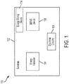
- FIG. 1 is a block diagram illustrating a microelectromechanical (MEMS) apparatus 100, in accordance with some embodiments.
- MEMS apparatus 100 includes a substrate 102, energy harvester 104, MEMS device 106 and electronic circuitry 108. Energy harvester 104 and MEMS device 106 are disposed on substrate 106. While electronic circuitry 108 is also shown as being disposed on substrate 102, not all embodiments are limited in this respect as the electronic circuitry may alternatively be positioned outside the substrate.
- Substrate 102 may be made using any suitable combination of materials.
- substrate 102 is made of silicon (e.g., single crystal silicon).
- Energy harvester 104 may be arranged to harvest energy from the surrounding environment and to power one or more electronic components, such as MEMS device 106, electronic circuitry 108, and/or other devices disposed on or outside substrate 102.
- Energy harvester 104 may harvest mechanical energy (e.g., vibrational energy), electromagnetic energy, solar energy, thermal energy or any other type of energy.
- MEMS apparatus 100 may include one or more energy storing devices 110 (such as batteries or super capacitors) for storing energy harvested by energy harvester 104.
- MEMS device 106 may include any suitable device fabricated using MEMS techniques.
- MEMS device 106 includes one or more inertial sensors, such as linear and/or angular accelerometers and gyroscopes.
- MEMS device 106 includes one or more resonators.
- the power necessary to generate the electric signals may be at least partially provided by energy harvester 104.
- Electronic circuitry 108 may include circuits for generating signals for driving MEMS device 106 and/or circuits for receiving signals generated by MEMS device 106. Additionally, or alternatively, electronic circuitry 108 may include circuits for performing other operations, such as for controlling the temperature of the substrate and/or for controlling other devices disposed on the substrate. Electronic circuitry 108 may be fabricated, at least in some embodiments, using complementary metal-oxide-semiconductors (CMOS) fabrication techniques. In the non-limiting embodiments in which MEMS device 106 includes one or more accelerometers, electronic circuitry 108 may include sense circuits for receiving sense signals generated by the accelerometer(s), and for determining the magnitude (and/or the direction) of the acceleration to which the accelerometer(s) are subjected.
- CMOS complementary metal-oxide-semiconductors
- electronic circuitry 108 may include sense circuits for sensing motion of the gyroscope(s) and/or drive circuits for driving the gyroscope(s)'s resonators.
- energy harvester 104 includes one or more piezoelectric energy harvesters and MEMS device 106 includes one or more accelerometers. It should be appreciated, however, that not all embodiments are limited to this specific arrangement.
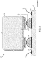
- FIG. 2 An example of such a MEMS apparatus is depicted in FIG. 2 , which illustrates an xz-plane cross sectional view.
- MEMS apparatus 200 includes a substrate 202 (which may serve as substrate 102) a proof mass 210, a plurality of connectors 212 coupling proof mass 210 to substrate 202, and inertial sensors 204, which are disposed between respective connectors 212 and proof mass 210.
- substrate 202 has a top surface 203, at least a portion of which being parallel to the xy-plane.
- Top surface 203 may represent the exposed surface of the substrate, such as the surface obtained through dicing, slicing, cleaving and/or etching of a silicon ingot.
- proof mass 210 has a height H along the z-axis, a width W along the x-axis and a depth D along the y-axis (not shown in FIG. 2 ). The height, width and depth of the proof mass may be chosen to provide a desired inertial response.
- the height H is sufficiently large to make the MEMS apparatus sensitive to low acceleration (such as less than 10ng or less than 1ng).
- height H may be between 100 ⁇ m and 5mm, between 300 ⁇ m and 5mm, between 500 ⁇ m and 5mm, between 500 ⁇ m and 3mm, between 500 ⁇ m and 2mm, between 500 ⁇ m and 1mm, between 600 ⁇ m and 1mm, between 700 ⁇ m and 700 ⁇ m, or any value or range within such ranges.
- MEMS apparatus 200 may be intended to be deployed in an environment predominantly subjected to low frequency vibrations (such as in wearable devices that are subject to body motion). As such, it may be desirable to set width W and depth D to be sufficiently large to enhance the response to vibrations in the low frequencies (e.g., less than 1KHz, less than 100Hz, less than 50Hz, or less than 10Hz).
- width W and depth D may be between 500 ⁇ m and 1cm, between 500 ⁇ m and 5mm, between 1mm and 1cm, between 1mm and 5mm, between 5cm and 10cm, or within any range within such ranges. Other ranges are also possible.
- motion of proof mass 210 may be leveraged to sense acceleration as well as to harvest energy.
- Inertial sensors 204 may comprise a plurality of layers, and may be configured to harvest mechanical energy generated when proof mass 210 vibrates. As such, in some embodiments, inertial sensors 204 are compliant, thus allowing for motion of proof mass 210 relative to substrate 202.
- at least one of the layers of inertial sensor 204 may be a piezoelectric material layer.
- the piezoelectric material layer may be arranged to generate electric charges when subjected to mechanical stress. Stress may arise, at least in some embodiments, when proof mass 210 moves relative to its position at rest. In one example, motion of the proof mass along the z-axis may cause the inertial sensor to flex, thus generating stress in the piezoelectric material layer. In response to the stress, the piezoelectric material may generate electric charges, which may be collected using conductive leads. In some embodiments, the electric energy generated in this manner may be used to at least partially power electronic circuitry which may be disposed on, in or outside substrate 202.
- inertial sensors 204 may be configured to sense motion of the proof mass 210. That is, inertial sensors 204 may generate electric signals that are indicative of the magnitude and/or direction of the motion of the proof mass.
- MEMS apparatus 200 operates as an accelerometer (as shown in FIG. 2 )
- the magnitude and/or direction of the acceleration to which the proof mass is subjected may be inferred from the sensed motion of the proof mass.
- MEMS apparatus 200 operates as a gyroscope
- the magnitude and/or direction of the angular velocity may be inferred from the sensed motion of the proof mass.
- MEMS apparatus 200 may operate as a 1-axis linear accelerometer (e.g., as a x-axis, y-axis, or z-axis linear accelerometer) as a 2-axis linear accelerometer (e.g., as a xy-plane linear accelerometer, xz-plane linear accelerometer or yz-plane linear accelerometer), as a 3-axis linear accelerometer, as a 1-axis angular accelerometer (e.g., as a x-axis, y-axis, or z-axis angular accelerometer) as a 2-axis angular accelerometer (e.g., as a xy-plane angular accelerometer, as a xz-plane angular accelerometer or as a yz-plane angular accelerometer), or as a 3-axis angular accelerometer.
- a 1-axis angular accelerometer e.g., as a x-axis, y-axi
- Motion of the proof mass may be sensed, at least in some embodiments, using capacitive sensors.
- inertial sensors 204 may comprise capacitors in some embodiments.
- the capacitors may be arranged such that the distance between their electrodes varies when the proof mass moves. Variations in the distance between the electrodes may lead to changes in the capacitance of the capacitor. Therefore, sense signals indicative of the motion of the proof mass may be generated in such embodiments by detecting variations in the capacitance.
- Connectors 212 may be implemented in any of numerous ways. Examples of connectors 212 include, but are not limited to, grid ball arrays, solder bumps (as shown in FIG. 2 ), and copper pillars. In some embodiments, connectors 212 are made of a conductive material, thus enabling transfer of electrical signals through them. For example, sense signals generated in response to motion of proof mass 210 and or electric energy generated by converting vibrational energy of the proof mass may be transferred via connectors 212.
- MEMS apparatus 200 includes conductive pads, which may be formed on top surface 203.
- the conductive pads may be electrically connected to connectors 212 via metal lines (not shown in FIG. 2 ).
- the metal lines may be buried in the substrate or may be routed on top surface 203.
- wire bonding to substrate 202 may be achieved by connecting wires 222 to conductive pads 220.
- sense signals generated in response to motion of the proof mass may be routed outside the substrate 202 via the wire bonds for further processing.
- the wire bonds may be used to transfer electric energy harvested by MEMS apparatus 200 outside substrate 202, thus powering other electronic circuits.
- sense circuitry for inferring the acceleration and/or velocity of the proof mass from the sense signals may be integrated in substrate 202.
- the sense circuitry is powered, at least partially, with the harvested electric energy.
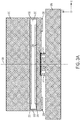
- inertial sensor 204 may comprise a beam 234, a piezoelectric material layer 238, a recess 230, conductive layer 239, and electrodes 235 and 236.
- beam 234 is made of the same material as proof mass 210, though not all embodiments are limited in this respect.
- beam 234 and proof mass 210 may be made of poly-silicon.
- Beam 234 may be connected to proof mass 210 through support 232. In some embodiments, multiple supports 232 may be used to connect the proof mass to the beam.
- support 232 may be wrapped around in the xy-plane, for example in a ring shape. In the example of FIG. 3A , support 232 is wrapped around the outer perimeter of recess 230. In some embodiments, recess 230 may be fully enclosed among proof mass 210, beam 234 and support(s) 232. In other embodiments, recess 230 may be only partially enclosed. For example, the support(s) may be arranged to only wrap around a portion of the outer perimeter of the recess 230.
- beam 234 may flex in response to acceleration.
- FIG. 3B-3C illustrate the inertial sensor of FIG. 3A , when subjected to acceleration directed opposite the z-axis, and in the direction of the z-axis, respectively.
- beam 234 may flex to allow motion of the proof mass 210.
- proof mass 210 moves towards the top surface 203 of substrate 202, and beam 234 flexes such that a concave surface 240 and a convex surface 242 are formed.
- Concave surface 240 may face the top surface 203 of substrate 202 while convex surface 242 may face away from top surface 203. As further illustrated in FIG. 3B , recess 230 may deform, relative to its shape at rest, when the proof mass 210 moves.
- the magnitude and/or direction of the acceleration may be sensed using a capacitive sensor. That is, the magnitude and/or direction of the acceleration may be inferred by sensing variations in the capacitance of a sense capacitor.
- the sense capacitors is formed between electrodes 235 and 236.
- electrode 235 may be disposed on beam 234, for example on the surface of the beam facing the proof mass 210.
- Electrode 236 may disposed on a surface of the proof mass 210, for example the outer surface of the proof mass that faces beam 234.
- Recess 320 may serve as the insulating material between the electrodes.
- the overall distance between electrodes 235 and 236 may decrease. That is, while the distance of some portions of the electrodes may remain substantially unchanged or even increase (such as the edges of electrode 235), the average distance between the electrodes considered across the electrodes' surfaces is decreased. As a result, the capacitance of the sense capacitor is increased relative to the rest position (when no acceleration is applied). This variation in capacitance may be detected by a sense circuit, which may be disposed on or outside substrate 202 and may be configured to infer the magnitude and/or direction of the acceleration based on the variation in capacitance.
- piezoelectric material layer 238, which may be formed on a surface of beam 234 (though in some embodiments, beam 234 may itself be made of a piezoelectric material), may flex with the beam in the presence of acceleration -a z .
- the piezoelectric material layer 238 may experience stress (e.g., tensile or compressive stress). The stress may in turn give rise to electric charges due to the piezoelectric effect.
- the piezoelectric material layer 238 may be viewed as a converter of vibrational energy to electric energy.
- piezoelectric material layer 238 may be made of any suitable piezoelectric material, such as materials having a piezoelectric coefficient d 33 (or d 31 ) that is greater, in absolute value, than 10 -13 m/V, 10 -12 m/V, 10 -11 m/V or 10 -10 m/V.
- materials that may be used for piezoelectric material 238 include, but are not limited to, lead zirconate titanate (PZT), aluminum nitride (A1N), or other group III-Nitride materials such as Gallium Nitride and Indium Nitride (InN).
- the electric charges generated in the piezoelectric material layer 238 in response to stress may be collected using conductive paths, and may be used to power one or more electronic devices or circuits.
- the conductive paths may be routed through conductive layer 239 (which may be disposed in contact with connectors 244 and may be, at least in some embodiments, made of nickel) and connectors 244 (shown in FIG. 3A , but not in FIGs. 3B-3C ) to substrate 202.
- These electric charges may be routed outside the substrate (e.g., via wires 222) or may power circuits disposed in the substrate.
- a circuit that may be powered using the electric charges generated by the piezoelectric material layer 238 is the sense circuitry described above.
- beam 234 may flex to allow motion of the proof mass 210 in a direction perpendicular to the substrate's top surface.
- proof mass 210 moves away from top surface 203 of substrate 202, and beam 234 flexes such that a concave surface 240 and a convex surface 242 are formed.
- Convex surface 242 may face the top surface 203 of substrate 202 while concave surface 240 may face away from top surface 203.
- recess 230 may deform, relative to its shape at rest.
- the overall distance between the electrodes 235 and 236 may increase, thus leading to a decrease in the capacitance of the sense capacitor. Such a decrease may be detected by the sense circuitry.
- the piezoelectric material layer 238 may flex with the beam 234, and as a result, electric charges may be generated. As in the case illustrated in FIG. 3B , the electric charges may be used to power electronic circuits or devices.
- motion of the proof mass 210 relative to the substrate in directions other than those parallel to the z-axis may cause stress in the piezoelectric material layer 238, and as a result, convert mechanical energy to electric energy. For example, when motion of the proof mass 210 occurs along the x-axis, mechanical energy may be transferred to beam 234 via support(s) 232, thus causing warping of beam 234.
- a gyroscope may be formed using proof mass 210.
- the gyroscope may comprise a resonator and a sensor.
- proof mass 210 is part of both the resonator and the sensor.
- the resonator may be driven using a drive circuit (which may be disposed in or outside substrate 202), which may be powered at least in part using the electricity generated with piezoelectric material layer 238.
- FIG. 4 illustrates a portion of piezoelectric material layer 238 in additional detail, in accordance with some embodiments.
- piezoelectric material layer 238 may be sandwiched between electrodes 402 and 404, which may be configured to form a capacitor with the piezoelectric material layer.
- Electrodes 402 and 404 may be made of any suitable conductive material, including but not limited to aluminum, copper and molybdenum.
- the piezoelectric material layer 238 and the electrodes 402 and 404 may be connected to beam 234 via dielectric layer 406, which may be a silicon oxide layer in some embodiments.
- dielectric layer 406 which may be a silicon oxide layer in some embodiments.
- electrode 404 is in contact with dielectric layer 406, which is in contact with beam 234.
- the inertial sensor of FIG. 3A may exhibit a rotational symmetry with respect to axis 350 (shown in FIG. 3A ), though not all embodiments are limited in this respect.
- piezoelectric material layer 238 may be shaped as a ring (or at least a portion of a ring) when viewed in the xy-plane.
- FIGs. 5A and 5B are two non-limiting examples illustrating how piezoelectric material layer 238 may be arranged in the xy-plane.
- piezoelectric material 239 is shaped as a ring having a gap 241. The two ends of the ring (labelled "+" and "-”) may serve as terminals.
- conductive lines 502 and 504 may be connected to the + and - ends and may be used to support currents when a voltage is generated between the + and - ends.
- Conductive line 502 may be connected to electrode 402 and conductive line 504 may be connected to electrode 404, though the opposite configuration is also possible.
- N gaps 241 may be formed along the length of the piezoelectric material layer 238, as shown in FIG. 5B .
- the voltage generated between the + and - terminals may increase by a factor N relative to the case shown in FIG. 5A .
- the electric charge, and as a result the electric current may decrease by a factor N relative to the case shown in FIG. 5A .
- the number of gaps may be chosen to provide a desired balance between current and voltage. For example, in applications in which it is desirable to generate a large current, the number of gaps may be decreased. Otherwise, in applications in which it is desirable to generate a large voltage, the number of gaps may be increased. It should be appreciated that the gaps illustrated in FIGs. 5A-5B are not necessarily limited to use in connection with piezoelectric material layers having rotational symmetry.
- the MEMS apparatus of FIG. 2 may be used to sense acceleration in one, two, or three dimensions, for example using multiple inertial sensors 204.
- Out-of-plane acceleration (in the z-axis direction) may be sensed by detecting common modes across the multiple sensors 204.
- In-plane acceleration (in the x-axis and/or the y-axis direction) may be sensed by detecting differential modes across the multiple sensors 204.
- FIG. 6A is a perspective view of a portion of a MEMS apparatus for sensing acceleration in three dimensions, in accordance with some embodiments.
- FIG. 6A illustrates the surface (labelled "S") of proof mass 210 that faces the top surface 203 of the substrate 202.
- proof mass 210 is coupled to five inertial sensors (204 A , 204 B , 204 C , 204 D and 204 E ) of the type described herein.
- inertial sensors 204 B and 204 D are aligned along the y-axis, and so are inertial sensors 204 A and 204 A .
- FIG. 6B is a top view of a substrate 202 that can be used in connection with the proof mass of FIG. 6A .
- the substrate comprises connectors 212 A , 212 B , 212 C , 212 D , and 212 E , which may be coupled, respectively, to inertial sensors 204 A , 204 B , 204 C , 204 D and 204 E .
- connectors 212 A , 212 B , 212 C , 212 D , and 212 E may be coupled, respectively, to conductive pads 220 A , 220 B , 220 C , 220 D and 220 E .
- Common mode signals across the conductive pads 220 A , 220 B , 220 C and 220 D may be used to detect acceleration in the z-axis direction. Acceleration in the y-axis direction may be detected by sensing differential mode signals between conductive pads 220 A and 220 C and/or between the conductive pads 220 B and 220 D . Acceleration in the x-axis direction may be detected by sensing differential mode signals between conductive pads 220 A and 220 B and/or between the conductive pads 220 C and 220 D .
- the signals obtained from conductive pad 220 E may be used for calibration ad may be coupled to a pressure sensor for measuring the pressure exercised in the inertial sensor 204 E .
- MEMS apparatuses of the types described herein are not limited to the specific number of inertial sensors or the specific arrangement illustrated in FIGs. 6A-6B , as any other suitable number of inertial sensors and arrangements may be used to sense acceleration in one, two or three dimensions.
- MEMS apparatus 100 may be deployed in various settings to detect acceleration, velocity and/or angular rates including sports, healthcare, scientific, military, and industrial applications, among others.
- MEMS apparatus 100 may be packaged in a wearable device deployed in monitoring sports-related physical activity and performance, patient health, military personnel activity, or other applications of interest of a user.
- MEMS apparatus 100 may be packaged in an implantable medical device, such as a pacemaker.
- MEMS apparatus 100 may be deployed in a wireless sensor node that is part of a network of sensors. In one specific application, the network of sensors may be configured to sense earthquakes.
- MEMS apparatus 100 may be disposed on a wearable device, as illustrated in FIG. 7 .
- MEMS apparatus 100 is disposed on a smartwatch 702.
- the MEMS apparatus may be arranged to enhance the energy harvested at low frequencies (such as the typical frequencies with which an arm 700 moves).
- proof mass 210 may be sufficiently large to enhance the proof mass vibrational response in the low frequencies.
- MEMS apparatus 100 may be configured to sense linear and/or angular acceleration, and to harvest mechanical energy produced by the motion of arm 700.
- aspects of the present application provide a inertial sensor configured to harvest energy from the surrounding environment.
- the inertial sensor and the energy harvester are disposed on the same substrate.
- energy captured through the harvester may be used to power the inertial sensor while avoiding power losses that may otherwise arise when transferring the energy from one substrate to another.
- aspects of the present application provide an inertial sensor configured to power itself. As such, the inertial sensor may be configured to operate without batteries, or at least to minimize battery usage.
Landscapes
- Physics & Mathematics (AREA)
- General Physics & Mathematics (AREA)
- Micromachines (AREA)
- Pressure Sensors (AREA)
- Gyroscopes (AREA)
Abstract
Description
- The present application relates to microelectromechanical systems (MEMS) inertial sensors.
- Some MEMS accelerometers include a proof mass configured to move in response to acceleration. The extent to which the proof mass moves provides an indication as to the magnitude of the acceleration. Some MEMS accelerometers use capacitive sensors to detect the amplitude of the proof mass' motion.
- According to one aspect of the present application, a microelectromechanical system (MEMS) apparatus is provided. The MEMS apparatus may comprise inertial sensors and energy harvesters configured to convert mechanical vibrational energy into electric energy. The harvested energy may be used to power an electronic circuit, such as the circuit used to sense acceleration with the inertial sensors. The inertial sensors and the energy harvesters may be disposed on the same substrate, and may share the same proof mass. The energy harvesters may include piezoelectric material layers disposed on a flexible structure. When the flexible structure flexes in response to vibration, stress arises in the piezoelectric material layer, which leads to the generation of electricity. Examples of inertial sensors include accelerometers and gyroscopes.
- According to another aspect of the present application, a microelectromechanical system (MEMS) apparatus is provided. The MEMS apparatus may comprise a substrate having a top surface; an inertial sensor comprising a proof mass coupled to the substrate, the inertial sensor being configured to sense motion of the proof mass along at least one axis; and an energy harvester comprising a piezoelectric material layer formed between the substrate and the proof mass, wherein the piezo electric material layer is configured to produce an electric signal in response to motion of the proof mass in a direction that is perpendicular to the top surface of the substrate.
- The at least one axis may be parallel to the top surface of the substrate.
- The at least one axis may be a first axis, and the inertial sensor may be further configured to sense motion of the proof mass along a second axis that is perpendicular to the first axis and parallel to the top surface of the substrate.
- The piezoelectric material layer may be formed on a beam disposed between the proof mass and the substrate.
- The inertial sensor may be configured to sense motion of the proof mass by sensing a variation in a capacitance of a sense capacitor formed between the proof mass and the beam.
- The beam may be configured to flex in response to motion of the proof mass relative to the top surface of the substrate.
- The proof mass and the beam may form a recess, the recess being configured to deform in response to motion of the proof mass relative to the top surface of the substrate.
- The inertial sensor may comprise an accelerometer configured to sense acceleration along the at least one axis by sensing motion of the proof mass along the at least one axis.
- According to another aspect of the present application, a microelectromechanical system (MEMS) apparatus is provided. THE MEMS apparatus may comprise a substrate; a piezoelectric energy harvester comprising: a beam coupled to the substrate, wherein at least a portion of the beam comprises a piezoelectric material layer; a proof mass coupled to the beam; and an inertial sensor comprising: a first electrode coupled to the proof mass; and a second electrode coupled to the beam.
- The piezoelectric material may be configured to generate an electric signal in response to out-of-plane motion of the proof mass.
- The inertial sensor may be configured to sense in-plane motion of the proof mass based on a sense signal generated by the first and second electrodes.
- The MEMS apparatus may further comprise a recess formed between the proof mass and the beam, wherein the first electrode is disposed within the recess.
- The piezoelectric energy harvester may further comprise third and fourth electrodes disposed on opposite sides of the piezoelectric material layer.
- The piezoelectric material layer may exhibit a rotational symmetry relative to an axis perpendicular to a top surface of the substrate and comprise one or more gaps.
- The proof mass preferably has a height that is between 500µm and 5mm.
- The inertial sensor may be first inertial sensor and the beam is a first beam, and the MEMS apparatus may further comprise a second inertial sensor having a third electrode coupled to the proof mass and a fourth electrode coupled to a second beam disposed between the substrate and the proof mass, wherein the first and second inertial sensors are configured to sense motion differentially.
- According to another aspect of the present application, a method for sensing motion using a microelectromechanical system (MEMS) apparatus is provided. The method may comprise converting, to electric energy, vibrational energy of a proof mass coupled to a substrate by sensing mechanical stress in a piezoelectric material layer formed between the proof mass and the substrate; with a sense circuit, sensing motion of the proof mass relative to the substrate along at least one axis; and powering the sense circuit at least in part with the electric energy.
- The at least one axis may be parallel to a top surface of the substrate.
- The piezoelectric material may be disposed on a beam formed between the proof mass and the substrate, and sensing mechanical stress in the piezoelectric material layer may comprise generating an electric signal is response to the mechanical stress.
- Sensing motion of the proof mass relative to the substrate may comprise sensing a variation in a capacitance of a sense capacitor formed between the proof mass and the beam.
- Various aspects and embodiments of the application will be described with reference to the following figures. It should be appreciated that the figures are not necessarily drawn to scale. Items appearing in multiple figures are indicated by the same reference number in all the figures in which they appear.
-
FIG. 1 is a block diagram illustrating a microelectromechanical system (MEMS) apparatus comprising an energy harvester and a MEMS device, according to some embodiments. -
FIG. 2 is a cross sectional view illustrating an example of a MEMS apparatus comprising an energy harvester and a MEMS device, according to some embodiments. -
FIG. 3A is a cross sectional view illustrating an example of an inertial sensor comprising a piezoelectric material layer, according to some embodiments. -
FIG. 3B illustrates the inertial sensor ofFIG. 3A when subjected to an acceleration directed opposite the z-axis, according to some embodiments. -
FIG. 3C illustrates the inertial sensor ofFIG. 3A when subjected to an acceleration in the direction of the z-axis, according to some embodiments. -
FIG. 4 is a cross sectional view illustrating a portion of the inertial sensor ofFIG. 3A in additional detail, according to some embodiments. -
FIGs. 5A-5B are top views illustrating possible layouts for the piezoelectric material layer ofFIG. 3A , according to some embodiments. -
FIG. 6A is a perspective view of a proof mass comprising a plurality of inertial sensors, according to some embodiments. -
FIG. 6B is a top view illustrating the top surface of a substrate that may be used in connection with the proof mass ofFIG. 6A , according to some embodiments. -
FIG. 7 is a schematic diagram illustrating a wearable device comprising the MEMS apparatus ofFIG. 1 , according to some embodiments. - Applicant has appreciated that, while MEMS devices (such as accelerometers, gyroscopes and resonators) are ubiquitous, the energy needed to power these devices is often limited, thus substantially restricting their usability. Certain sensor nodes, for example, are deployed in very remote locations, which can substantially increase the cost incurred to periodically replace the batteries. In another example, gyroscopes are mounted in smartphones and rely on the smartphone's battery for power. However, the batteries are shared among a variety of devices mounted in the smartphone, such as speakers, microphones, displays, the processors, etc. As a result, battery runtime is often as short as a few hours, thus limiting the time in which the gyroscopes can operate.
- Applicant has appreciated that the usability of MEMS devices may be enhanced by equipping the MEMS devices with energy harvesters for capturing energy from the surrounding environment. In this way, the MEMS device's reliance on external power sources such as batteries may be limited, or even eliminated in some circumstances. Some aspects of the present application relate to MEMS apparatuses having a MEMS device (e.g., an inertial sensor) and an energy harvester disposed on the same substrate. Being on the same substrate, the location in which the power is generated and the location in which the power is used are close to one another, thus eliminating power losses that may otherwise arise if the MEMS device and the energy harvester were disposed on separate substrates. In some embodiments, the energy harvester may comprise a layer of piezoelectric material configured to generate electric charges when subjected to mechanical stress, thus converting mechanical energy into electric energy.
- In some embodiments, the MEMS device includes an accelerometer configured to sense linear and/or angular acceleration. The piezoelectric energy harvester and the accelerometer may share the same proof mass. In these embodiments, motion of the proof mass in response to acceleration may have two effects: first, it may cause the energy harvester to capture at least some of the mechanical energy generated by the motion; second, it may cause the accelerometer to detect a signal indicative to the acceleration to which the proof mass is subjected.
- Some MEMS apparatuses of the types described herein may be configured to capture energy from out-of-plane motion (e.g., towards or away from the substrate) of the proof mass and to detect out-of-plane motion of the proof mass. Other MEMS apparatuses of the types described herein may be configured to capture energy from out-of-plane motion of the proof mass and to detect in-plane motion (e.g., in a plane parallel to the substrate) of the proof mass. Yet other apparatuses of the types described herein may be configured to capture energy from out-of-plane motion of the proof mass and to detect in-plane and out-of-plane motion of the proof mass.
-
FIG. 1 is a block diagram illustrating a microelectromechanical (MEMS)apparatus 100, in accordance with some embodiments.MEMS apparatus 100 includes asubstrate 102,energy harvester 104,MEMS device 106 andelectronic circuitry 108.Energy harvester 104 andMEMS device 106 are disposed onsubstrate 106. Whileelectronic circuitry 108 is also shown as being disposed onsubstrate 102, not all embodiments are limited in this respect as the electronic circuitry may alternatively be positioned outside the substrate. -
Substrate 102 may be made using any suitable combination of materials. In some embodiments,substrate 102 is made of silicon (e.g., single crystal silicon).Energy harvester 104 may be arranged to harvest energy from the surrounding environment and to power one or more electronic components, such asMEMS device 106,electronic circuitry 108, and/or other devices disposed on oroutside substrate 102.Energy harvester 104 may harvest mechanical energy (e.g., vibrational energy), electromagnetic energy, solar energy, thermal energy or any other type of energy. Optionally,MEMS apparatus 100 may include one or more energy storing devices 110 (such as batteries or super capacitors) for storing energy harvested byenergy harvester 104. -
MEMS device 106 may include any suitable device fabricated using MEMS techniques. In one example,MEMS device 106 includes one or more inertial sensors, such as linear and/or angular accelerometers and gyroscopes. In another example,MEMS device 106 includes one or more resonators. In the examples in whichMEMS device 106 includes active components, that is, devices configured to be driven with electric signals, the power necessary to generate the electric signals may be at least partially provided byenergy harvester 104. -
Electronic circuitry 108 may include circuits for generating signals for drivingMEMS device 106 and/or circuits for receiving signals generated byMEMS device 106. Additionally, or alternatively,electronic circuitry 108 may include circuits for performing other operations, such as for controlling the temperature of the substrate and/or for controlling other devices disposed on the substrate.Electronic circuitry 108 may be fabricated, at least in some embodiments, using complementary metal-oxide-semiconductors (CMOS) fabrication techniques. In the non-limiting embodiments in whichMEMS device 106 includes one or more accelerometers,electronic circuitry 108 may include sense circuits for receiving sense signals generated by the accelerometer(s), and for determining the magnitude (and/or the direction) of the acceleration to which the accelerometer(s) are subjected. In the non-limiting embodiments in which the MEMS device includes one or more gyroscopes,electronic circuitry 108 may include sense circuits for sensing motion of the gyroscope(s) and/or drive circuits for driving the gyroscope(s)'s resonators. - In one specific example,
energy harvester 104 includes one or more piezoelectric energy harvesters andMEMS device 106 includes one or more accelerometers. It should be appreciated, however, that not all embodiments are limited to this specific arrangement. An example of such a MEMS apparatus is depicted inFIG. 2 , which illustrates an xz-plane cross sectional view.MEMS apparatus 200 includes a substrate 202 (which may serve as substrate 102) aproof mass 210, a plurality ofconnectors 212 couplingproof mass 210 tosubstrate 202, andinertial sensors 204, which are disposed betweenrespective connectors 212 andproof mass 210. - In some embodiments,
substrate 202 has atop surface 203, at least a portion of which being parallel to the xy-plane.Top surface 203 may represent the exposed surface of the substrate, such as the surface obtained through dicing, slicing, cleaving and/or etching of a silicon ingot. As illustrated inFIG. 2 ,proof mass 210 has a height H along the z-axis, a width W along the x-axis and a depth D along the y-axis (not shown inFIG. 2 ). The height, width and depth of the proof mass may be chosen to provide a desired inertial response. In some embodiments, the height H is sufficiently large to make the MEMS apparatus sensitive to low acceleration (such as less than 10ng or less than 1ng). For example, height H may be between 100µm and 5mm, between 300µm and 5mm, between 500µm and 5mm, between 500µm and 3mm, between 500µm and 2mm, between 500µm and 1mm, between 600µm and 1mm, between 700µm and 700µm, or any value or range within such ranges. - In some embodiments,
MEMS apparatus 200 may be intended to be deployed in an environment predominantly subjected to low frequency vibrations (such as in wearable devices that are subject to body motion). As such, it may be desirable to set width W and depth D to be sufficiently large to enhance the response to vibrations in the low frequencies (e.g., less than 1KHz, less than 100Hz, less than 50Hz, or less than 10Hz). For example, width W and depth D may be between 500µm and 1cm, between 500µm and 5mm, between 1mm and 1cm, between 1mm and 5mm, between 5cm and 10cm, or within any range within such ranges. Other ranges are also possible. In at least some of the embodiments in which MEMS apparatus includes one or more accelerometers and one or more energy harvesters, motion ofproof mass 210 may be leveraged to sense acceleration as well as to harvest energy. -
Inertial sensors 204 may comprise a plurality of layers, and may be configured to harvest mechanical energy generated whenproof mass 210 vibrates. As such, in some embodiments,inertial sensors 204 are compliant, thus allowing for motion ofproof mass 210 relative tosubstrate 202. In one example, at least one of the layers ofinertial sensor 204 may be a piezoelectric material layer. The piezoelectric material layer may be arranged to generate electric charges when subjected to mechanical stress. Stress may arise, at least in some embodiments, whenproof mass 210 moves relative to its position at rest. In one example, motion of the proof mass along the z-axis may cause the inertial sensor to flex, thus generating stress in the piezoelectric material layer. In response to the stress, the piezoelectric material may generate electric charges, which may be collected using conductive leads. In some embodiments, the electric energy generated in this manner may be used to at least partially power electronic circuitry which may be disposed on, in oroutside substrate 202. - In some embodiments,
inertial sensors 204 may be configured to sense motion of theproof mass 210. That is,inertial sensors 204 may generate electric signals that are indicative of the magnitude and/or direction of the motion of the proof mass. In the embodiments in whichMEMS apparatus 200 operates as an accelerometer (as shown inFIG. 2 ), the magnitude and/or direction of the acceleration to which the proof mass is subjected may be inferred from the sensed motion of the proof mass. However, in the embodiments in whichMEMS apparatus 200 operates as a gyroscope, the magnitude and/or direction of the angular velocity may be inferred from the sensed motion of the proof mass.MEMS apparatus 200 may operate as a 1-axis linear accelerometer (e.g., as a x-axis, y-axis, or z-axis linear accelerometer) as a 2-axis linear accelerometer (e.g., as a xy-plane linear accelerometer, xz-plane linear accelerometer or yz-plane linear accelerometer), as a 3-axis linear accelerometer, as a 1-axis angular accelerometer (e.g., as a x-axis, y-axis, or z-axis angular accelerometer) as a 2-axis angular accelerometer (e.g., as a xy-plane angular accelerometer, as a xz-plane angular accelerometer or as a yz-plane angular accelerometer), or as a 3-axis angular accelerometer. - Motion of the proof mass may be sensed, at least in some embodiments, using capacitive sensors. As such,
inertial sensors 204 may comprise capacitors in some embodiments. The capacitors may be arranged such that the distance between their electrodes varies when the proof mass moves. Variations in the distance between the electrodes may lead to changes in the capacitance of the capacitor. Therefore, sense signals indicative of the motion of the proof mass may be generated in such embodiments by detecting variations in the capacitance. -
Connectors 212 may be implemented in any of numerous ways. Examples ofconnectors 212 include, but are not limited to, grid ball arrays, solder bumps (as shown inFIG. 2 ), and copper pillars. In some embodiments,connectors 212 are made of a conductive material, thus enabling transfer of electrical signals through them. For example, sense signals generated in response to motion ofproof mass 210 and or electric energy generated by converting vibrational energy of the proof mass may be transferred viaconnectors 212. - In some embodiments,
MEMS apparatus 200 includes conductive pads, which may be formed ontop surface 203. The conductive pads may be electrically connected toconnectors 212 via metal lines (not shown inFIG. 2 ). The metal lines may be buried in the substrate or may be routed ontop surface 203. In some embodiments, wire bonding tosubstrate 202 may be achieved by connectingwires 222 toconductive pads 220. In some embodiments, sense signals generated in response to motion of the proof mass may be routed outside thesubstrate 202 via the wire bonds for further processing. In some embodiments, the wire bonds may be used to transfer electric energy harvested byMEMS apparatus 200outside substrate 202, thus powering other electronic circuits. It should be appreciated that, in some embodiments, sense circuitry for inferring the acceleration and/or velocity of the proof mass from the sense signals may be integrated insubstrate 202. In some embodiments, the sense circuitry is powered, at least partially, with the harvested electric energy. - A non-limiting example of an
inertial sensor 204 is depicted inFIG. 3A , in accordance with some embodiments. As illustrated,inertial sensor 204 may comprise abeam 234, apiezoelectric material layer 238, arecess 230, conductive layer 239, andelectrodes beam 234 is made of the same material asproof mass 210, though not all embodiments are limited in this respect. For example,beam 234 andproof mass 210 may be made of poly-silicon.Beam 234 may be connected toproof mass 210 throughsupport 232. In some embodiments,multiple supports 232 may be used to connect the proof mass to the beam. In some embodiments,support 232 may be wrapped around in the xy-plane, for example in a ring shape. In the example ofFIG. 3A ,support 232 is wrapped around the outer perimeter ofrecess 230. In some embodiments,recess 230 may be fully enclosed amongproof mass 210,beam 234 and support(s) 232. In other embodiments,recess 230 may be only partially enclosed. For example, the support(s) may be arranged to only wrap around a portion of the outer perimeter of therecess 230. - In some embodiments,
beam 234 may flex in response to acceleration.FIG. 3B-3C illustrate the inertial sensor ofFIG. 3A , when subjected to acceleration directed opposite the z-axis, and in the direction of the z-axis, respectively. As depicted inFIG. 3B , when the inertial sensor is subjected to an acceleration -az directed opposite the z-axis,beam 234 may flex to allow motion of theproof mass 210. In this example,proof mass 210 moves towards thetop surface 203 ofsubstrate 202, andbeam 234 flexes such that aconcave surface 240 and aconvex surface 242 are formed.Concave surface 240 may face thetop surface 203 ofsubstrate 202 whileconvex surface 242 may face away fromtop surface 203. As further illustrated inFIG. 3B ,recess 230 may deform, relative to its shape at rest, when theproof mass 210 moves. - In some embodiments, the magnitude and/or direction of the acceleration may be sensed using a capacitive sensor. That is, the magnitude and/or direction of the acceleration may be inferred by sensing variations in the capacitance of a sense capacitor. In the configurations shown in
FIGs. 3A-3C , the sense capacitors is formed betweenelectrodes electrode 235 may be disposed onbeam 234, for example on the surface of the beam facing theproof mass 210.Electrode 236 may disposed on a surface of theproof mass 210, for example the outer surface of the proof mass that facesbeam 234. Recess 320 (whether filled with a dielectric material, air or other types of gas or in vacuum), may serve as the insulating material between the electrodes. - When
proof mass 210 moves opposite the z-axis, as illustrated inFIG. 3B , the overall distance betweenelectrodes outside substrate 202 and may be configured to infer the magnitude and/or direction of the acceleration based on the variation in capacitance. - As further illustrated in
FIG. 3B ,piezoelectric material layer 238, which may be formed on a surface of beam 234 (though in some embodiments,beam 234 may itself be made of a piezoelectric material), may flex with the beam in the presence of acceleration -az . When flexed, thepiezoelectric material layer 238 may experience stress (e.g., tensile or compressive stress). The stress may in turn give rise to electric charges due to the piezoelectric effect. As such, thepiezoelectric material layer 238 may be viewed as a converter of vibrational energy to electric energy. It should be appreciated thatpiezoelectric material layer 238 may be made of any suitable piezoelectric material, such as materials having a piezoelectric coefficient d33 (or d31) that is greater, in absolute value, than 10-13 m/V, 10-12 m/V, 10-11 m/V or 10-10 m/V. Examples of materials that may be used forpiezoelectric material 238 include, but are not limited to, lead zirconate titanate (PZT), aluminum nitride (A1N), or other group III-Nitride materials such as Gallium Nitride and Indium Nitride (InN). - In some embodiments, the electric charges generated in the
piezoelectric material layer 238 in response to stress may be collected using conductive paths, and may be used to power one or more electronic devices or circuits. The conductive paths may be routed through conductive layer 239 (which may be disposed in contact withconnectors 244 and may be, at least in some embodiments, made of nickel) and connectors 244 (shown inFIG. 3A , but not inFIGs. 3B-3C ) tosubstrate 202. These electric charges may be routed outside the substrate (e.g., via wires 222) or may power circuits disposed in the substrate. One example of a circuit that may be powered using the electric charges generated by thepiezoelectric material layer 238 is the sense circuitry described above. - The case in which an acceleration is applied in the same direction as the z-axis is depicted in
FIG. 3C . As illustrated,beam 234 may flex to allow motion of theproof mass 210 in a direction perpendicular to the substrate's top surface. In this case,proof mass 210 moves away fromtop surface 203 ofsubstrate 202, andbeam 234 flexes such that aconcave surface 240 and aconvex surface 242 are formed.Convex surface 242 may face thetop surface 203 ofsubstrate 202 whileconcave surface 240 may face away fromtop surface 203. As further illustrated inFIG. 3C ,recess 230 may deform, relative to its shape at rest. In this case, the overall distance between theelectrodes FIG. 3C , thepiezoelectric material layer 238 may flex with thebeam 234, and as a result, electric charges may be generated. As in the case illustrated inFIG. 3B , the electric charges may be used to power electronic circuits or devices. It should be appreciated that motion of theproof mass 210 relative to the substrate in directions other than those parallel to the z-axis may cause stress in thepiezoelectric material layer 238, and as a result, convert mechanical energy to electric energy. For example, when motion of theproof mass 210 occurs along the x-axis, mechanical energy may be transferred tobeam 234 via support(s) 232, thus causing warping ofbeam 234. - While the inertial sensor of
FIGs. 3A-3C has been described as operating as an accelerometer, it should be appreciated that any other suitable types of inertial sensor may operate according to the techniques described herein. For example, in some embodiments, a gyroscope may be formed usingproof mass 210. The gyroscope may comprise a resonator and a sensor. In some embodiments,proof mass 210 is part of both the resonator and the sensor. The resonator may be driven using a drive circuit (which may be disposed in or outside substrate 202), which may be powered at least in part using the electricity generated withpiezoelectric material layer 238. -
FIG. 4 illustrates a portion ofpiezoelectric material layer 238 in additional detail, in accordance with some embodiments. In some embodiments,piezoelectric material layer 238 may be sandwiched betweenelectrodes piezoelectric material 238 in response to stress may give rise to a voltage betweenelectrodes Electrodes piezoelectric material layer 238 and theelectrodes beam 234 viadielectric layer 406, which may be a silicon oxide layer in some embodiments. In one specific example,electrode 404 is in contact withdielectric layer 406, which is in contact withbeam 234. - In some embodiments, the inertial sensor of
FIG. 3A may exhibit a rotational symmetry with respect to axis 350 (shown inFIG. 3A ), though not all embodiments are limited in this respect. In some such embodiments,piezoelectric material layer 238 may be shaped as a ring (or at least a portion of a ring) when viewed in the xy-plane.FIGs. 5A and 5B are two non-limiting examples illustrating howpiezoelectric material layer 238 may be arranged in the xy-plane. In the example ofFIG. 5A , piezoelectric material 239 is shaped as a ring having agap 241. The two ends of the ring (labelled "+" and "-") may serve as terminals. That is,conductive lines Conductive line 502 may be connected toelectrode 402 andconductive line 504 may be connected toelectrode 404, though the opposite configuration is also possible. - In other embodiments,
N gaps 241 may be formed along the length of thepiezoelectric material layer 238, as shown inFIG. 5B . In this arrangement, the voltage generated between the + and - terminals may increase by a factor N relative to the case shown inFIG. 5A . However, the electric charge, and as a result the electric current, may decrease by a factor N relative to the case shown inFIG. 5A . As such, the number of gaps may be chosen to provide a desired balance between current and voltage. For example, in applications in which it is desirable to generate a large current, the number of gaps may be decreased. Otherwise, in applications in which it is desirable to generate a large voltage, the number of gaps may be increased. It should be appreciated that the gaps illustrated inFIGs. 5A-5B are not necessarily limited to use in connection with piezoelectric material layers having rotational symmetry. - The MEMS apparatus of
FIG. 2 may be used to sense acceleration in one, two, or three dimensions, for example using multipleinertial sensors 204. Out-of-plane acceleration (in the z-axis direction) may be sensed by detecting common modes across themultiple sensors 204. In-plane acceleration (in the x-axis and/or the y-axis direction) may be sensed by detecting differential modes across themultiple sensors 204. -
FIG. 6A is a perspective view of a portion of a MEMS apparatus for sensing acceleration in three dimensions, in accordance with some embodiments. In particular,FIG. 6A illustrates the surface (labelled "S") ofproof mass 210 that faces thetop surface 203 of thesubstrate 202. In this configuration,proof mass 210 is coupled to five inertial sensors (204A, 204B, 204C, 204D and 204E) of the type described herein. In some embodiments,inertial sensors inertial sensors inertial sensors inertial sensors FIG. 6B is a top view of asubstrate 202 that can be used in connection with the proof mass ofFIG. 6A . In this case, the substrate comprisesconnectors inertial sensors connectors conductive pads - Common mode signals across the
conductive pads conductive pads conductive pads conductive pads conductive pads conductive pad 220E may be used for calibration ad may be coupled to a pressure sensor for measuring the pressure exercised in theinertial sensor 204E. It should be appreciated that MEMS apparatuses of the types described herein are not limited to the specific number of inertial sensors or the specific arrangement illustrated inFIGs. 6A-6B , as any other suitable number of inertial sensors and arrangements may be used to sense acceleration in one, two or three dimensions. -
MEMS apparatus 100 may be deployed in various settings to detect acceleration, velocity and/or angular rates including sports, healthcare, scientific, military, and industrial applications, among others. In some embodiments,MEMS apparatus 100 may be packaged in a wearable device deployed in monitoring sports-related physical activity and performance, patient health, military personnel activity, or other applications of interest of a user. In someembodiments MEMS apparatus 100 may be packaged in an implantable medical device, such as a pacemaker. In some embodiments,MEMS apparatus 100 may be deployed in a wireless sensor node that is part of a network of sensors. In one specific application, the network of sensors may be configured to sense earthquakes. - In one illustrative example,
MEMS apparatus 100 may be disposed on a wearable device, as illustrated inFIG. 7 . In this case,MEMS apparatus 100 is disposed on asmartwatch 702. The MEMS apparatus may be arranged to enhance the energy harvested at low frequencies (such as the typical frequencies with which anarm 700 moves). For example,proof mass 210 may be sufficiently large to enhance the proof mass vibrational response in the low frequencies.MEMS apparatus 100 may be configured to sense linear and/or angular acceleration, and to harvest mechanical energy produced by the motion ofarm 700. - Aspects of the present application may provide one or more benefits, some of which have been previously described. Now described are some non-limiting examples of such benefits. It should be appreciated that not all aspects and embodiments necessarily provide all of the benefits now described. Further, it should be appreciated that aspects of the present application may provide additional benefits to those now described.
- Aspects of the present application provide a inertial sensor configured to harvest energy from the surrounding environment. In some embodiments, the inertial sensor and the energy harvester are disposed on the same substrate. As a result, energy captured through the harvester may be used to power the inertial sensor while avoiding power losses that may otherwise arise when transferring the energy from one substrate to another. Aspects of the present application provide an inertial sensor configured to power itself. As such, the inertial sensor may be configured to operate without batteries, or at least to minimize battery usage.
Claims (16)
- A microelectromechanical system (MEMS) apparatus comprising:a substrate having a top surface;an inertial sensor comprising a proof mass coupled to the substrate, the inertial sensor being configured to sense motion of the proof mass along at least one axis; andan energy harvester comprising a piezoelectric material layer formed between the substrate and the proof mass, wherein the piezo electric material layer is configured to produce an electric signal in response to motion of the proof mass relative to the top surface of the substrate.
- The MEMS apparatus of claim 1, wherein the at least one axis is parallel to the top surface of the substrate.
- The MEMS apparatus of claim 2, wherein the at least one axis is a first axis, and wherein the inertial sensor is further configured to sense motion of the proof mass along a second axis that is perpendicular to the first axis and parallel to the top surface of the substrate.
- The MEMS apparatus of any preceding claim, wherein the piezoelectric material layer is formed on a beam disposed between the proof mass and the substrate.
- The MEMS apparatus of claim 4, wherein at least one of the following applies:the inertial sensor is configured to sense motion of the proof mass by sensing a variation in a capacitance of a sense capacitor formed between the proof mass and the beam;the beam is configured to flex in response to motion of the proof mass relative to the top surface of the substrate; andthe proof mass and the beam form a recess, the recess being configured to deform in response to motion of the proof mass relative to the top surface of the substrate.
- The MEMS apparatus of claim 1, wherein the inertial sensor comprises an accelerometer configured to sense acceleration along the at least one axis by sensing motion of the proof mass along the at least one axis.
- A microelectromechanical system (MEMS) apparatus comprising:a substrate;a piezoelectric energy harvester comprising:a beam coupled to the substrate, wherein at least a portion of the beam comprises a piezoelectric material layer;a proof mass coupled to the beam; andan inertial sensor comprising:a first electrode coupled to the proof mass; anda second electrode coupled to the beam.
- The MEMS apparatus of claim 7, wherein the piezoelectric material is configured to generate an electric signal in response to out-of-plane motion of the proof mass.
- The MEMS apparatus of claim 7 or 8, wherein the inertial sensor is configured to sense in-plane motion of the proof mass based on a sense signal generated by the first and second electrodes.
- The MEMS apparatus of claim 7, 8 or 9, further comprising a recess formed between the proof mass and the beam, wherein the first electrode is disposed within the recess.
- The MEMS apparatus of claim 9, wherein at least one of the following applies:the piezoelectric energy harvester further comprises third and fourth electrodes disposed on opposite sides of the piezoelectric material layer;the piezoelectric material layer exhibits a rotational symmetry relative to an axis perpendicular to a top surface of the substrate and comprises one or more gaps; andthe proof mass has a height that is between 500µm and 5mm.
- The MEMS apparatus of claim 9, wherein the inertial sensor is a first inertial sensor and the beam is a first beam, and wherein:the MEMS apparatus further comprises a second inertial sensor having a third electrode coupled to the proof mass and a fourth electrode coupled to a second beam disposed between the substrate and the proof mass, wherein the first and second inertial sensors are configured to sense motion differentially.
- A method for sensing motion using a microelectromechanical system (MEMS) apparatus, the method comprising:converting, to electric energy, vibrational energy of a proof mass coupled to a substrate by sensing mechanical stress in a piezoelectric material layer formed between the proof mass and the substrate;with a sense circuit, sensing motion of the proof mass relative to the substrate along at least one axis; andpowering the sense circuit at least in part with the electric energy.
- The method of claim 13, wherein the at least one axis is parallel to a top surface of the substrate.
- The method of claim 13 or 14, wherein the piezoelectric material is disposed on a beam formed between the proof mass and the substrate, and wherein sensing mechanical stress in the piezoelectric material layer comprises generating an electric signal is response to the mechanical stress.
- The method of claim 15, wherein sensing motion of the proof mass relative to the substrate comprises sensing a variation in a capacitance of a sense capacitor formed between the proof mass and the beam.
Applications Claiming Priority (1)
| Application Number | Priority Date | Filing Date | Title |
|---|---|---|---|
| US15/818,713 US10761108B2 (en) | 2017-11-20 | 2017-11-20 | Microelectromechanical systems (MEMS) inertial sensors with energy harvesters and related methods |
Publications (2)
| Publication Number | Publication Date |
|---|---|
| EP3486661A1 true EP3486661A1 (en) | 2019-05-22 |
| EP3486661B1 EP3486661B1 (en) | 2020-06-24 |
Family
ID=64172413
Family Applications (1)
| Application Number | Title | Priority Date | Filing Date |
|---|---|---|---|
| EP18204427.1A Active EP3486661B1 (en) | 2017-11-20 | 2018-11-05 | Microelectromechanical systems (mems) inertial sensors with energy harvesters and related methods |
Country Status (4)
| Country | Link |
|---|---|
| US (1) | US10761108B2 (en) |
| EP (1) | EP3486661B1 (en) |
| CN (1) | CN109813932B (en) |
| DE (1) | DE102018128130B4 (en) |
Cited By (1)
| Publication number | Priority date | Publication date | Assignee | Title |
|---|---|---|---|---|
| CN115340060A (en) * | 2022-08-26 | 2022-11-15 | 南京高华科技股份有限公司 | Raindrop energy collector and preparation method thereof |
Families Citing this family (9)
| Publication number | Priority date | Publication date | Assignee | Title |
|---|---|---|---|---|
| US11279614B2 (en) * | 2019-06-28 | 2022-03-22 | Analog Devices, Inc. | Low-parasitic capacitance MEMS inertial sensors and related methods |
| CN111678510A (en) * | 2019-12-13 | 2020-09-18 | 中北大学 | A MEMS energy harvester |
| IT202000005563A1 (en) * | 2020-03-16 | 2021-09-16 | St Microelectronics Srl | MEMS INERTIAL SENSOR WITH HIGH RESISTANCE TO THE PHENOMENON OF ADHESION |
| US11519726B2 (en) * | 2020-06-19 | 2022-12-06 | Analog Devices, Inc. | Mechanism for selective coupling in microelectromechanical systems inertial sensors |
| US12139396B2 (en) * | 2020-08-07 | 2024-11-12 | Stmicroelectronics S.R.L. | Microelectromechanical sensor device with improved stability to stress |
| US11714102B2 (en) | 2021-06-08 | 2023-08-01 | Analog Devices, Inc. | Fully differential accelerometer |
| US11879906B2 (en) | 2021-11-18 | 2024-01-23 | Invensense, Inc. | Inertial sensor sensing of vibration frequency |
| US12227409B2 (en) | 2021-12-09 | 2025-02-18 | Invensense, Inc. | Robust inertial sensor self-test |
| CN115360292B (en) * | 2022-09-20 | 2025-12-26 | 上海凸申科技有限公司 | A piezoelectric thin film sensor |
Citations (4)
| Publication number | Priority date | Publication date | Assignee | Title |
|---|---|---|---|---|
| US20100236329A1 (en) * | 2009-03-23 | 2010-09-23 | Omnitek Partners Llc | Methods and apparatus for integrated energy harvesting power sources and inertial sensors for gun-fired munitions |
| WO2011042611A1 (en) * | 2009-10-08 | 2011-04-14 | Vti Technologies Oy | Method and device for energy harvesting |
| US20170118542A1 (en) * | 2015-10-27 | 2017-04-27 | The Boeing Company | System and method for data retransmission through rf opaque barriers |
| EP3185320A1 (en) * | 2015-12-24 | 2017-06-28 | STMicroelectronics S.r.l. | Mems piezoelectric device and corresponding manufacturing process |
Family Cites Families (36)
| Publication number | Priority date | Publication date | Assignee | Title |
|---|---|---|---|---|
| US7231874B2 (en) * | 2001-09-05 | 2007-06-19 | Omnitek Partners Llc | Power supplies for projectiles and other devices |
| EP1803168A4 (en) * | 2004-10-21 | 2009-05-20 | Michelin Soc Tech | MINIATURIZED PIEZOELECTRIC COLLECTOR OF VIBRATION ENERGY |
| US7327003B2 (en) | 2005-02-15 | 2008-02-05 | Analog Devices, Inc. | Sensor system |
| US20070125176A1 (en) * | 2005-12-02 | 2007-06-07 | Honeywell International, Inc. | Energy harvesting device and methods |
| US20080074002A1 (en) | 2006-09-26 | 2008-03-27 | Shashank Priya | Piezoelectric energy harvester |
| US7839058B1 (en) | 2007-01-29 | 2010-11-23 | Microstrain, Inc. | Wideband vibration energy harvester |
| US20080296984A1 (en) * | 2007-05-29 | 2008-12-04 | Sanyo Electric Co., Ltd. | Energy converter |
| US8011237B2 (en) * | 2008-02-22 | 2011-09-06 | Hong Kong Applied Science And Technology Research Institute Co., Ltd. | Piezoelectric module for energy harvesting, such as in a tire pressure monitoring system |
| CN102144355B (en) | 2008-09-09 | 2014-03-19 | 株式会社村田制作所 | piezoelectric generator |
| EP2302712A1 (en) | 2009-09-28 | 2011-03-30 | Stichting IMEC Nederland | Method for resonance frequency tuning of micromachined structures |
| KR101243868B1 (en) | 2009-12-14 | 2013-03-20 | 한국전자통신연구원 | The active piezoelectric energy harvester having embedded variable capacitance layer and manufacturing method thereof |
| JP2011221002A (en) * | 2010-03-25 | 2011-11-04 | Sanyo Electric Co Ltd | Vibration detection device, air pressure detection terminal and acceleration detection system |
| JP5627279B2 (en) * | 2010-04-28 | 2014-11-19 | パナソニック株式会社 | Vibration power generation device and manufacturing method thereof |
| US20110291526A1 (en) | 2010-05-27 | 2011-12-01 | Innowattech Ltd. | Piezoelectric stack compression generator |
| EP2399676A1 (en) * | 2010-06-25 | 2011-12-28 | Stichting IMEC Nederland | Method and device for vibration harvesting via gasflow |
| US8410665B2 (en) * | 2010-12-23 | 2013-04-02 | Taiwan Semiconductor Manufacturing Company, Ltd. | MEMS kinetic energy conversion |
| US8680752B2 (en) * | 2011-02-11 | 2014-03-25 | Georgia Tech Research Corporation | Piezoelectric micromechanical energy harvesters |
| US8759990B2 (en) * | 2011-04-19 | 2014-06-24 | Eastman Kodak Company | Energy harvesting device including MEMS composite transducer |
| US8680695B2 (en) * | 2011-04-19 | 2014-03-25 | Eastman Kodak Company | Energy harvesting using MEMS composite transducer |
| JP2013102639A (en) * | 2011-11-09 | 2013-05-23 | Panasonic Corp | Environment power generation device |
| US8633634B2 (en) | 2011-11-18 | 2014-01-21 | The Board Of Regents Of The University Of Texas System | MEMs-based cantilever energy harvester |
| KR20130055867A (en) | 2011-11-21 | 2013-05-29 | 한국전자통신연구원 | Piezoelectric micro power generator and fabrication method thereof |
| US9076961B2 (en) * | 2012-01-31 | 2015-07-07 | Duality Reality Energy, LLC | Energy harvesting with a micro-electro-machanical system (MEMS) |
| KR101388142B1 (en) | 2012-07-11 | 2014-04-23 | 전자부품연구원 | Piezo power generator for power feeding of mobile terminal |
| CA2827946A1 (en) * | 2012-09-19 | 2014-03-19 | The Governors Of The University Of Alberta | Piezoelectric apparatus for harvesting energy for portable electronics and method for manufacturing same |
| US9484522B2 (en) * | 2013-03-13 | 2016-11-01 | Microgen Systems, Inc. | Piezoelectric energy harvester device with curved sidewalls, system, and methods of use and making |
| AU2014229323B2 (en) * | 2013-03-14 | 2016-08-11 | Raviv Erlich | MEMS hinges with enhanced rotatability |
| JP6249203B2 (en) * | 2013-05-17 | 2017-12-20 | パナソニックIpマネジメント株式会社 | Power generation vibration sensor, tire and electric device using the same |
| US9711711B2 (en) * | 2013-07-03 | 2017-07-18 | Texas Instruments Incorporated | Piecewise piezoelectric energy harvester |
| US9716446B2 (en) * | 2013-07-05 | 2017-07-25 | Texas Instruments Incorporated | Self-powered piezoelectric energy harvesting microsystem |
| WO2015036869A2 (en) * | 2013-09-13 | 2015-03-19 | Meggitt A/S | Piezoelectric energy harvesting |
| SG10201408210UA (en) * | 2013-11-22 | 2015-06-29 | Agency Science Tech & Res | Energy harvesting device and method for forming the same |
| US10263173B2 (en) * | 2015-01-16 | 2019-04-16 | The Regents Of The University Of Michigan | Multi-axis piezoelectric transducer |
| US9874459B2 (en) * | 2015-02-24 | 2018-01-23 | The Regents Of The University Of Michigan | Actuation and sensing platform for sensor calibration and vibration isolation |
| WO2017070187A1 (en) | 2015-10-19 | 2017-04-27 | Massachusetts Institute Of Technology | Micro electromechanical system (mems) energy harvester with residual stress induced instability |
| US10536098B2 (en) | 2016-02-12 | 2020-01-14 | Analog Devices, Inc. | Piezoelectric energy harvester for human motion |
-
2017
- 2017-11-20 US US15/818,713 patent/US10761108B2/en active Active
-
2018
- 2018-11-05 EP EP18204427.1A patent/EP3486661B1/en active Active
- 2018-11-09 DE DE102018128130.7A patent/DE102018128130B4/en active Active
- 2018-11-20 CN CN201811379525.5A patent/CN109813932B/en active Active
Patent Citations (4)
| Publication number | Priority date | Publication date | Assignee | Title |
|---|---|---|---|---|
| US20100236329A1 (en) * | 2009-03-23 | 2010-09-23 | Omnitek Partners Llc | Methods and apparatus for integrated energy harvesting power sources and inertial sensors for gun-fired munitions |
| WO2011042611A1 (en) * | 2009-10-08 | 2011-04-14 | Vti Technologies Oy | Method and device for energy harvesting |
| US20170118542A1 (en) * | 2015-10-27 | 2017-04-27 | The Boeing Company | System and method for data retransmission through rf opaque barriers |
| EP3185320A1 (en) * | 2015-12-24 | 2017-06-28 | STMicroelectronics S.r.l. | Mems piezoelectric device and corresponding manufacturing process |
Cited By (2)
| Publication number | Priority date | Publication date | Assignee | Title |
|---|---|---|---|---|
| CN115340060A (en) * | 2022-08-26 | 2022-11-15 | 南京高华科技股份有限公司 | Raindrop energy collector and preparation method thereof |
| CN115340060B (en) * | 2022-08-26 | 2024-03-08 | 南京高华科技股份有限公司 | Raindrop energy collector and preparation method thereof |
Also Published As
| Publication number | Publication date |
|---|---|
| CN109813932A (en) | 2019-05-28 |
| US20190154725A1 (en) | 2019-05-23 |
| US10761108B2 (en) | 2020-09-01 |
| CN109813932B (en) | 2021-10-29 |
| EP3486661B1 (en) | 2020-06-24 |
| DE102018128130B4 (en) | 2022-02-03 |
| DE102018128130A1 (en) | 2019-05-23 |
Similar Documents
| Publication | Publication Date | Title |
|---|---|---|
| EP3486661B1 (en) | Microelectromechanical systems (mems) inertial sensors with energy harvesters and related methods | |
| EP3644066B1 (en) | Low-noise multi-axis accelerometers and related methods | |
| KR102464039B1 (en) | Anchor tracking devices and related methods for in-plane accelerometers | |
| US10732198B2 (en) | Integrated linear and angular MEMS accelerometers | |
| US10816569B2 (en) | Z axis accelerometer using variable vertical gaps | |
| US10948294B2 (en) | MEMS gyroscopes with in-line springs and related systems and methods | |
| US11137248B2 (en) | Sensor element, inertial sensor, and electronic apparatus | |
| CA3013265A1 (en) | Multiple degree of freedom mems sensor chip and method for fabricating the same | |
| CA3004760A1 (en) | 3d mems magnetometer and associated methods | |
| CN103080707A (en) | Vibration sensor | |
| CN110169085A (en) | The system of the non-acoustic sensor combined with MEMS microphone | |
| US10001372B2 (en) | Angular velocity detection device | |
| CN106053883B (en) | Physical quantity sensor, electronic apparatus, and moving object | |
| KR20160122712A (en) | Packaged piezoelectric energy harvester device with a compliant stopper structure, system, and methods of use and making | |
| JP6056177B2 (en) | Gyro sensor, electronic equipment | |
| JP2016176891A (en) | Angular velocity detection element, angular velocity detection device, electronic apparatus and moving object | |
| JP2016176892A (en) | Angular velocity detection element, angular velocity detection device, electronic apparatus and mobile body | |
| WO2007061056A1 (en) | Sensor device and method for manufacturing same | |
| JP2012237664A (en) | Physical quantity sensor and electronic apparatus | |
| JP2018112466A (en) | Sensor device and electronic equipment | |
| WO2018189545A1 (en) | A vibration-based energy harvester comprising a proof mass surrounding a central anchor | |
| JP6922325B2 (en) | Physical quantity sensors, physical quantity sensor devices, electronic devices and mobiles | |
| WO2008039834A2 (en) | Leveraged shear mode accelerometers | |
| Stoeckel et al. | Wake up MEMS for inertial sensors | |
| CN113678000B (en) | Physical quantity sensor |
Legal Events
| Date | Code | Title | Description |
|---|---|---|---|
| PUAI | Public reference made under article 153(3) epc to a published international application that has entered the european phase |
Free format text: ORIGINAL CODE: 0009012 |
|
| STAA | Information on the status of an ep patent application or granted ep patent |
Free format text: STATUS: THE APPLICATION HAS BEEN PUBLISHED |
|
| AK | Designated contracting states |
Kind code of ref document: A1 Designated state(s): AL AT BE BG CH CY CZ DE DK EE ES FI FR GB GR HR HU IE IS IT LI LT LU LV MC MK MT NL NO PL PT RO RS SE SI SK SM TR |
|
| AX | Request for extension of the european patent |
Extension state: BA ME |
|
| STAA | Information on the status of an ep patent application or granted ep patent |
Free format text: STATUS: REQUEST FOR EXAMINATION WAS MADE |
|
| GRAP | Despatch of communication of intention to grant a patent |
Free format text: ORIGINAL CODE: EPIDOSNIGR1 |
|
| STAA | Information on the status of an ep patent application or granted ep patent |
Free format text: STATUS: GRANT OF PATENT IS INTENDED |
|
| 17P | Request for examination filed |
Effective date: 20191107 |
|
| RBV | Designated contracting states (corrected) |
Designated state(s): AL AT BE BG CH CY CZ DE DK EE ES FI FR GB GR HR HU IE IS IT LI LT LU LV MC MK MT NL NO PL PT RO RS SE SI SK SM TR |
|
| INTG | Intention to grant announced |
Effective date: 20191213 |
|
| GRAJ | Information related to disapproval of communication of intention to grant by the applicant or resumption of examination proceedings by the epo deleted |
Free format text: ORIGINAL CODE: EPIDOSDIGR1 |
|
| STAA | Information on the status of an ep patent application or granted ep patent |
Free format text: STATUS: REQUEST FOR EXAMINATION WAS MADE |
|
| GRAR | Information related to intention to grant a patent recorded |
Free format text: ORIGINAL CODE: EPIDOSNIGR71 |
|
| GRAS | Grant fee paid |
Free format text: ORIGINAL CODE: EPIDOSNIGR3 |
|
| STAA | Information on the status of an ep patent application or granted ep patent |
Free format text: STATUS: GRANT OF PATENT IS INTENDED |
|
| GRAA | (expected) grant |
Free format text: ORIGINAL CODE: 0009210 |
|
| STAA | Information on the status of an ep patent application or granted ep patent |
Free format text: STATUS: THE PATENT HAS BEEN GRANTED |
|
| INTC | Intention to grant announced (deleted) | ||
| INTG | Intention to grant announced |
Effective date: 20200514 |
|
| AK | Designated contracting states |
Kind code of ref document: B1 Designated state(s): AL AT BE BG CH CY CZ DE DK EE ES FI FR GB GR HR HU IE IS IT LI LT LU LV MC MK MT NL NO PL PT RO RS SE SI SK SM TR |
|
| REG | Reference to a national code |
Ref country code: GB Ref legal event code: FG4D |
|
| REG | Reference to a national code |
Ref country code: CH Ref legal event code: EP |
|
| REG | Reference to a national code |
Ref country code: DE Ref legal event code: R096 Ref document number: 602018005556 Country of ref document: DE |
|
| REG | Reference to a national code |
Ref country code: AT Ref legal event code: REF Ref document number: 1284409 Country of ref document: AT Kind code of ref document: T Effective date: 20200715 |
|
| REG | Reference to a national code |
Ref country code: IE Ref legal event code: FG4D |
|
| PG25 | Lapsed in a contracting state [announced via postgrant information from national office to epo] |
Ref country code: SE Free format text: LAPSE BECAUSE OF FAILURE TO SUBMIT A TRANSLATION OF THE DESCRIPTION OR TO PAY THE FEE WITHIN THE PRESCRIBED TIME-LIMIT Effective date: 20200624 Ref country code: FI Free format text: LAPSE BECAUSE OF FAILURE TO SUBMIT A TRANSLATION OF THE DESCRIPTION OR TO PAY THE FEE WITHIN THE PRESCRIBED TIME-LIMIT Effective date: 20200624 Ref country code: NO Free format text: LAPSE BECAUSE OF FAILURE TO SUBMIT A TRANSLATION OF THE DESCRIPTION OR TO PAY THE FEE WITHIN THE PRESCRIBED TIME-LIMIT Effective date: 20200924 Ref country code: GR Free format text: LAPSE BECAUSE OF FAILURE TO SUBMIT A TRANSLATION OF THE DESCRIPTION OR TO PAY THE FEE WITHIN THE PRESCRIBED TIME-LIMIT Effective date: 20200925 Ref country code: LT Free format text: LAPSE BECAUSE OF FAILURE TO SUBMIT A TRANSLATION OF THE DESCRIPTION OR TO PAY THE FEE WITHIN THE PRESCRIBED TIME-LIMIT Effective date: 20200624 |
|
| REG | Reference to a national code |
Ref country code: LT Ref legal event code: MG4D |
|
| PG25 | Lapsed in a contracting state [announced via postgrant information from national office to epo] |
Ref country code: RS Free format text: LAPSE BECAUSE OF FAILURE TO SUBMIT A TRANSLATION OF THE DESCRIPTION OR TO PAY THE FEE WITHIN THE PRESCRIBED TIME-LIMIT Effective date: 20200624 Ref country code: LV Free format text: LAPSE BECAUSE OF FAILURE TO SUBMIT A TRANSLATION OF THE DESCRIPTION OR TO PAY THE FEE WITHIN THE PRESCRIBED TIME-LIMIT Effective date: 20200624 Ref country code: BG Free format text: LAPSE BECAUSE OF FAILURE TO SUBMIT A TRANSLATION OF THE DESCRIPTION OR TO PAY THE FEE WITHIN THE PRESCRIBED TIME-LIMIT Effective date: 20200924 Ref country code: HR Free format text: LAPSE BECAUSE OF FAILURE TO SUBMIT A TRANSLATION OF THE DESCRIPTION OR TO PAY THE FEE WITHIN THE PRESCRIBED TIME-LIMIT Effective date: 20200624 |
|
| REG | Reference to a national code |
Ref country code: NL Ref legal event code: MP Effective date: 20200624 |
|
| REG | Reference to a national code |
Ref country code: AT Ref legal event code: MK05 Ref document number: 1284409 Country of ref document: AT Kind code of ref document: T Effective date: 20200624 |
|
| PG25 | Lapsed in a contracting state [announced via postgrant information from national office to epo] |
Ref country code: NL Free format text: LAPSE BECAUSE OF FAILURE TO SUBMIT A TRANSLATION OF THE DESCRIPTION OR TO PAY THE FEE WITHIN THE PRESCRIBED TIME-LIMIT Effective date: 20200624 Ref country code: AL Free format text: LAPSE BECAUSE OF FAILURE TO SUBMIT A TRANSLATION OF THE DESCRIPTION OR TO PAY THE FEE WITHIN THE PRESCRIBED TIME-LIMIT Effective date: 20200624 |
|
| PG25 | Lapsed in a contracting state [announced via postgrant information from national office to epo] |
Ref country code: IT Free format text: LAPSE BECAUSE OF FAILURE TO SUBMIT A TRANSLATION OF THE DESCRIPTION OR TO PAY THE FEE WITHIN THE PRESCRIBED TIME-LIMIT Effective date: 20200624 Ref country code: RO Free format text: LAPSE BECAUSE OF FAILURE TO SUBMIT A TRANSLATION OF THE DESCRIPTION OR TO PAY THE FEE WITHIN THE PRESCRIBED TIME-LIMIT Effective date: 20200624 Ref country code: EE Free format text: LAPSE BECAUSE OF FAILURE TO SUBMIT A TRANSLATION OF THE DESCRIPTION OR TO PAY THE FEE WITHIN THE PRESCRIBED TIME-LIMIT Effective date: 20200624 Ref country code: SM Free format text: LAPSE BECAUSE OF FAILURE TO SUBMIT A TRANSLATION OF THE DESCRIPTION OR TO PAY THE FEE WITHIN THE PRESCRIBED TIME-LIMIT Effective date: 20200624 Ref country code: PT Free format text: LAPSE BECAUSE OF FAILURE TO SUBMIT A TRANSLATION OF THE DESCRIPTION OR TO PAY THE FEE WITHIN THE PRESCRIBED TIME-LIMIT Effective date: 20201026 Ref country code: AT Free format text: LAPSE BECAUSE OF FAILURE TO SUBMIT A TRANSLATION OF THE DESCRIPTION OR TO PAY THE FEE WITHIN THE PRESCRIBED TIME-LIMIT Effective date: 20200624 Ref country code: CZ Free format text: LAPSE BECAUSE OF FAILURE TO SUBMIT A TRANSLATION OF THE DESCRIPTION OR TO PAY THE FEE WITHIN THE PRESCRIBED TIME-LIMIT Effective date: 20200624 Ref country code: ES Free format text: LAPSE BECAUSE OF FAILURE TO SUBMIT A TRANSLATION OF THE DESCRIPTION OR TO PAY THE FEE WITHIN THE PRESCRIBED TIME-LIMIT Effective date: 20200624 |
|
| PG25 | Lapsed in a contracting state [announced via postgrant information from national office to epo] |
Ref country code: SK Free format text: LAPSE BECAUSE OF FAILURE TO SUBMIT A TRANSLATION OF THE DESCRIPTION OR TO PAY THE FEE WITHIN THE PRESCRIBED TIME-LIMIT Effective date: 20200624 Ref country code: PL Free format text: LAPSE BECAUSE OF FAILURE TO SUBMIT A TRANSLATION OF THE DESCRIPTION OR TO PAY THE FEE WITHIN THE PRESCRIBED TIME-LIMIT Effective date: 20200624 Ref country code: IS Free format text: LAPSE BECAUSE OF FAILURE TO SUBMIT A TRANSLATION OF THE DESCRIPTION OR TO PAY THE FEE WITHIN THE PRESCRIBED TIME-LIMIT Effective date: 20201024 |
|
| REG | Reference to a national code |
Ref country code: DE Ref legal event code: R097 Ref document number: 602018005556 Country of ref document: DE |
|
| PG25 | Lapsed in a contracting state [announced via postgrant information from national office to epo] |
Ref country code: DK Free format text: LAPSE BECAUSE OF FAILURE TO SUBMIT A TRANSLATION OF THE DESCRIPTION OR TO PAY THE FEE WITHIN THE PRESCRIBED TIME-LIMIT Effective date: 20200624 |
|
| PLBE | No opposition filed within time limit |
Free format text: ORIGINAL CODE: 0009261 |
|
| STAA | Information on the status of an ep patent application or granted ep patent |
Free format text: STATUS: NO OPPOSITION FILED WITHIN TIME LIMIT |
|
| 26N | No opposition filed |
Effective date: 20210325 |
|
| PG25 | Lapsed in a contracting state [announced via postgrant information from national office to epo] |
Ref country code: MC Free format text: LAPSE BECAUSE OF FAILURE TO SUBMIT A TRANSLATION OF THE DESCRIPTION OR TO PAY THE FEE WITHIN THE PRESCRIBED TIME-LIMIT Effective date: 20200624 |
|
| PG25 | Lapsed in a contracting state [announced via postgrant information from national office to epo] |
Ref country code: LU Free format text: LAPSE BECAUSE OF NON-PAYMENT OF DUE FEES Effective date: 20201105 |
|
| REG | Reference to a national code |
Ref country code: BE Ref legal event code: MM Effective date: 20201130 |
|
| PG25 | Lapsed in a contracting state [announced via postgrant information from national office to epo] |
Ref country code: SI Free format text: LAPSE BECAUSE OF FAILURE TO SUBMIT A TRANSLATION OF THE DESCRIPTION OR TO PAY THE FEE WITHIN THE PRESCRIBED TIME-LIMIT Effective date: 20200624 |
|
| PG25 | Lapsed in a contracting state [announced via postgrant information from national office to epo] |
Ref country code: IE Free format text: LAPSE BECAUSE OF NON-PAYMENT OF DUE FEES Effective date: 20201105 |
|
| PG25 | Lapsed in a contracting state [announced via postgrant information from national office to epo] |
Ref country code: TR Free format text: LAPSE BECAUSE OF FAILURE TO SUBMIT A TRANSLATION OF THE DESCRIPTION OR TO PAY THE FEE WITHIN THE PRESCRIBED TIME-LIMIT Effective date: 20200624 Ref country code: MT Free format text: LAPSE BECAUSE OF FAILURE TO SUBMIT A TRANSLATION OF THE DESCRIPTION OR TO PAY THE FEE WITHIN THE PRESCRIBED TIME-LIMIT Effective date: 20200624 Ref country code: CY Free format text: LAPSE BECAUSE OF FAILURE TO SUBMIT A TRANSLATION OF THE DESCRIPTION OR TO PAY THE FEE WITHIN THE PRESCRIBED TIME-LIMIT Effective date: 20200624 |
|
| PG25 | Lapsed in a contracting state [announced via postgrant information from national office to epo] |
Ref country code: MK Free format text: LAPSE BECAUSE OF FAILURE TO SUBMIT A TRANSLATION OF THE DESCRIPTION OR TO PAY THE FEE WITHIN THE PRESCRIBED TIME-LIMIT Effective date: 20200624 |
|
| REG | Reference to a national code |
Ref country code: CH Ref legal event code: PL |
|
| PG25 | Lapsed in a contracting state [announced via postgrant information from national office to epo] |
Ref country code: BE Free format text: LAPSE BECAUSE OF NON-PAYMENT OF DUE FEES Effective date: 20201130 |
|
| PG25 | Lapsed in a contracting state [announced via postgrant information from national office to epo] |
Ref country code: LI Free format text: LAPSE BECAUSE OF NON-PAYMENT OF DUE FEES Effective date: 20211130 Ref country code: CH Free format text: LAPSE BECAUSE OF NON-PAYMENT OF DUE FEES Effective date: 20211130 |
|
| PGFP | Annual fee paid to national office [announced via postgrant information from national office to epo] |
Ref country code: DE Payment date: 20251022 Year of fee payment: 8 |
|
| PGFP | Annual fee paid to national office [announced via postgrant information from national office to epo] |
Ref country code: GB Payment date: 20251023 Year of fee payment: 8 |
|
| PGFP | Annual fee paid to national office [announced via postgrant information from national office to epo] |
Ref country code: FR Payment date: 20251022 Year of fee payment: 8 |