EP3485535B1 - Structure composite à caractéristiques diélectriques reconfigurables et ensemble comprenant une telle structure composite - Google Patents
Structure composite à caractéristiques diélectriques reconfigurables et ensemble comprenant une telle structure composite Download PDFInfo
- Publication number
- EP3485535B1 EP3485535B1 EP17751030.2A EP17751030A EP3485535B1 EP 3485535 B1 EP3485535 B1 EP 3485535B1 EP 17751030 A EP17751030 A EP 17751030A EP 3485535 B1 EP3485535 B1 EP 3485535B1
- Authority
- EP
- European Patent Office
- Prior art keywords
- composite
- composite structure
- family
- dispersed
- active
- Prior art date
- Legal status (The legal status is an assumption and is not a legal conclusion. Google has not performed a legal analysis and makes no representation as to the accuracy of the status listed.)
- Active
Links
Images


Classifications
-
- H—ELECTRICITY
- H01—ELECTRIC ELEMENTS
- H01Q—ANTENNAS, i.e. RADIO AERIALS
- H01Q15/00—Devices for reflection, refraction, diffraction or polarisation of waves radiated from an antenna, e.g. quasi-optical devices
- H01Q15/0006—Devices acting selectively as reflecting surface, as diffracting or as refracting device, e.g. frequency filtering or angular spatial filtering devices
- H01Q15/006—Selective devices having photonic band gap materials or materials of which the material properties are frequency dependent, e.g. perforated substrates, high-impedance surfaces
- H01Q15/0066—Selective devices having photonic band gap materials or materials of which the material properties are frequency dependent, e.g. perforated substrates, high-impedance surfaces said selective devices being reconfigurable, tunable or controllable, e.g. using switches
-
- H—ELECTRICITY
- H05—ELECTRIC TECHNIQUES NOT OTHERWISE PROVIDED FOR
- H05K—PRINTED CIRCUITS; CASINGS OR CONSTRUCTIONAL DETAILS OF ELECTRIC APPARATUS; MANUFACTURE OF ASSEMBLAGES OF ELECTRICAL COMPONENTS
- H05K1/00—Printed circuits
- H05K1/02—Details
- H05K1/0213—Electrical arrangements not otherwise provided for
- H05K1/0216—Reduction of cross-talk, noise or electromagnetic interference
- H05K1/0236—Electromagnetic band-gap structures
-
- H—ELECTRICITY
- H05—ELECTRIC TECHNIQUES NOT OTHERWISE PROVIDED FOR
- H05K—PRINTED CIRCUITS; CASINGS OR CONSTRUCTIONAL DETAILS OF ELECTRIC APPARATUS; MANUFACTURE OF ASSEMBLAGES OF ELECTRICAL COMPONENTS
- H05K1/00—Printed circuits
- H05K1/02—Details
- H05K1/03—Use of materials for the substrate
- H05K1/0313—Organic insulating material
- H05K1/0353—Organic insulating material consisting of two or more materials, e.g. two or more polymers, polymer + filler, + reinforcement
-
- H—ELECTRICITY
- H05—ELECTRIC TECHNIQUES NOT OTHERWISE PROVIDED FOR
- H05K—PRINTED CIRCUITS; CASINGS OR CONSTRUCTIONAL DETAILS OF ELECTRIC APPARATUS; MANUFACTURE OF ASSEMBLAGES OF ELECTRICAL COMPONENTS
- H05K2201/00—Indexing scheme relating to printed circuits covered by H05K1/00
- H05K2201/01—Dielectrics
- H05K2201/0183—Dielectric layers
- H05K2201/0187—Dielectric layers with regions of different dielectrics in the same layer, e.g. in a printed capacitor for locally changing the dielectric properties
-
- H—ELECTRICITY
- H05—ELECTRIC TECHNIQUES NOT OTHERWISE PROVIDED FOR
- H05K—PRINTED CIRCUITS; CASINGS OR CONSTRUCTIONAL DETAILS OF ELECTRIC APPARATUS; MANUFACTURE OF ASSEMBLAGES OF ELECTRICAL COMPONENTS
- H05K2201/00—Indexing scheme relating to printed circuits covered by H05K1/00
- H05K2201/10—Details of components or other objects attached to or integrated in a printed circuit board
- H05K2201/10007—Types of components
- H05K2201/10098—Components for radio transmission, e.g. radio frequency identification [RFID] tag, printed or non-printed antennas
Definitions
- the present invention relates to a composite structure with reconfigurable dielectric characteristics.
- the invention relates in particular to multifunctional active composite structures having both a structural function and one or more functionalities in the field of microwave applications, for example in terms of stealth, shielding, integration or decoupling of antennas, or a radome function.
- the substrates in composite materials whether monolithic or sandwich, have complex dielectric characteristics (real part + imaginary part) defined for a given composition of the structure and at a given working frequency. These dielectric characteristics are fixed and not reconfigurable in the existing.
- Such substrates can be integrated into a microwave system consisting for example of a radome made of composite materials and the antenna housed, or of a printed circuit on a substrate made of composite material, or of an antenna integrated into a wall structural in composite material.
- a microwave system can consist of an antenna and a wall formed of a substrate made of a composite material, which is for example the carrier wall of the antenna or a radome.
- the reconfigurability of such a microwave system is generally ensured by the antenna, via the use of active and electrically controllable components such as pin diodes, varicaps, transistors and / or MEMS, the substrate made of composite material having a totally passive function.
- An objective of the invention is therefore to propose a composite structure having reconfigurable dielectric properties and which is suitable both for use as a carrier wall of an antenna or as a radome, and for use on a large scale as a structural panel, in particular of a naval, land or air carrier.
- the invention relates to a composite structure according to claim 1.
- the structure according to the invention may include one or more of the features of claims 2 to 9.
- the invention also relates to an assembly according to claim 10.
- the composite structure comprises a composite substrate and a plurality of active charges dispersed in the composite substrate.
- the active charges are formed from a piezoelectric material, the dielectric characteristics of which can be modified by applying a command to the composite structure, therefore to the active charges.
- the piezoelectric material is for example also pyroelectric, i.e. piezoelectric and pyroelectric.
- the piezoelectric material can also be ferroelectric, i.e. be piezoelectric, pyroelectric and ferroelectric.
- the dielectric characteristics of the composite structure including these charges are themselves modifiable, therefore reconfigurable, by application of this command.
- the complex dielectric permittivity of the active charges, and therefore of the structure integrating them, can be modified by application of a suitable command, so as to vary the absorption and reflection properties by the composite structure of electromagnetic waves incident on it. composite substrate.
- the complex electrical permittivity of active charges depends on the control applied to the charges.
- the complex dielectric permittivity of the active charges can therefore be modified by application of a command.
- the complex dielectric permittivity of the active charges can be modified by applying a mechanical command.
- the complex dielectric permittivity of the active charges can be modified by applying a mechanical, thermal or optical command.
- the complex dielectric permittivity of the active charges can be modified by application of a mechanical, thermal, optical or electrical command.
- the active charges are made of a ferroelectric material, which therefore also has piezoelectric and pyroelectric properties.
- the complex electrical permittivity of the active charges can be modified by applying an electrical command, a thermal command, an optical command, and / or a mechanical command.
- the active charges are for example dispersed throughout the substrate.
- the dielectric characteristics of the entire composite structure can be reconfigured.
- the active charges are, for example, uniformly dispersed in the substrate.
- the active charges are dispersed locally, in a localized portion or several localized portions of the composite substrate.
- the dielectric characteristics of the portion (s) of the composite structure comprising active charges can be reconfigured. In this portion or in each of these portions, the active charges are for example dispersed uniformly.
- the active charges are for example formed of a ferroelectric material which is preferably chosen from the family of perovskites, the ilmenite family, the family of pyrochlores, the family of quadratic bronzes, the family of Aurivillius phases, the chosen material possibly doped.
- the ferroelectric material is for example a material of the perovskite family, for example BaTiO 3 , CaTiO 3 , KTaO 3 , YMnO 3 , PbTiO 3 , etc.
- the ferroelectric material can be a doped phase of one of the above materials, for example Ba 1-x SrTiO 3 , KTa 1-x Nb x TiO 3 , AgTa 1-x Nb x O 3 , Sr 1-x Bi x TiO 3 , Pb 1-x Sr x TiO 3 , BaZr 1-x Ti x O 3 etc.
- the value of the coefficient x can be chosen between 0 and 1, depending in particular on the desired Curie temperature for the material.
- the ferroelectric material can also be a multiferroic material, for example BiFeO 3 , having several ferroic properties.
- the material is both ferroelectric, ferroelastic and ferromagnetic.
- the active charges then consist of a mixture of at least two ferroelectric materials.
- control in particular electrical, thermal, optical or mechanical, can be applied to the entire composite structure, so as to control the dielectric characteristics uniformly throughout the composite structure, or to only a portion of the composite structure, so as to control the dielectric characteristics of this portion of the composite structure, independently of the rest of the composite structure.
- a different command can be applied to the rest of the composite structure.
- an electrical control comprises the application of a difference in electrical potential to at least a portion of the composite structure, for example a potential difference imposed between the two faces of the composite structure, resulting in a modification of the permittivity complex electrical active charges, therefore of the selected portion of the composite structure or of the entire composite structure.
- a thermal control is carried out by imposing on at least a portion of the composite structure a given temperature, resulting in a modification of the complex electrical permittivity of the active charges in this portion.
- the composite structure can be associated, for example, with one or more resistors arranged around the periphery of the composite structure.
- An optical control is for example carried out by directing an optical source, for example a laser source, on a localized portion of the composite structure or on the whole of the composite structure, so as to generate in the localized portion, or in the whole structure, a rise in temperature, resulting in a modification of the complex electrical permittivity of the active charges in this localized portion or in the whole of the composite structure.
- an optical source for example a laser source
- a mechanical control includes the application of a mechanical stress, in compression or in tension, to a localized portion or to the whole of the composite structure, resulting in a modification of the complex electrical permittivity of the active charges in this localized portion or throughout the composite structure.
- the magnetic characteristics of the composite structure can also be modified by applying a magnetic command.
- control is applied by a control device, which is configured to apply an electrical, thermal, mechanical, optical and / or magnetic control to the structure, to the portion of the composite structure containing the active charges, or to a selected part of the composite structure.
- thermal control is more particularly suitable for controlling the overall dielectric characteristics of the composite structure, while the use of an optical or electrical control is in particular suitable for locally varying the dielectric characteristics of the composite structure .
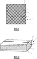
- the composite structure 1 comprises a composite substrate 3 made of a monolithic composite material.
- This monolithic composite material comprising an impregnation resin 5, forming the matrix of the composite material, and a set of fibrous reinforcements 7, which provide the mechanical reinforcement of the composite substrate.
- the resin 5 is preferably an organic, thermosetting or thermoplastic resin, for example a polymer resin such as an epoxy resin, a polyester resin, vinyl ester, etc.
- the reinforcements 7 are made of an organic or inorganic material. These are, for example, glass or carbon fibers.
- the composite structure 1 also comprises a plurality of active charges 9 which are dispersed in the composite substrate 3.
- the active charges 9 are dispersed, in powder form, in the impregnation resin 5.
- the active fillers 9 are for example introduced by mixing into the resin before it hardens.
- the rate of dispersed active charges is chosen so as to optimize the reconfigurability of the composite structure 1, that is to say in an amount sufficient to allow a significant modification of the dielectric characteristics of the composite structure 1, while preserving the resin its mechanical performance and above all its ability to serve as an impregnation matrix for fibrous reinforcements 7.
- the charge rate expressed as a percentage by mass in the resin matrix, is between 50% and 90%.
- a reduction in the rate of charge of active charges induces a reduction in the reconfigurability properties of the composite structure comprising these charges, while an increase in this charge rate can induce embrittlement of the composite structure and make it more difficult to achieve.
- the active fillers are dispersed in the form of powder on the reinforcements 7.
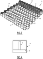
- the composite structure 11 comprises a sandwich composite substrate 13.
- the sandwich composite substrate 13 comprises a core 15 interposed between two skins 17.
- the core 15 is for example made of an expanded material or foam, which is for example a foam of polyethersufone, polyvinyl chloride, polyurethane, polyethylene, polystyrene, or polymethacrylimide.
- the core 15 is made of a material having a honeycomb structure of the honeycomb type, this honeycomb structure comprising transverse walls delimiting a plurality of cells. These cells are for example through, that is to say open transversely on either side of the core 15.
- the cellular structure is for example made of aluminum or a thermosetting or thermoplastic material such as polypropylene, or still in aramid paper.
- Each skin 17 is made of a rigid material, for example a monolithic composite material as described with reference to the first embodiment, comprising an impregnation resin and a set of fibrous reinforcements
- the composite structure 11 comprises a plurality of active charges which are dispersed in the core 15 and / or in at least one of the skins 17.
- the core 15 is made of a material having a honeycomb type honeycomb structure, and the active charges are dispersed in the core 15, in particular in at least one part alveoli.
- At least a first set of cells i.e. a part of the cells, includes active charges.
- the active charges are introduced into the cells in the form of a powder of ferroelectric material.
- the powder formed of active charges is directly introduced into the cells.
- the active charges are introduced into the cells in the form of powder after sintering (ceramic).
- the active charges can also be dispersed in an organic resin or in an expanded material introduced into the cells.
- the charge rate of active charges in this resin is chosen so as to optimize the reconfigurability of the composite structure 11.
- the cells with such active charges are selected according to the intended application.
- a core 15 of a composite sandwich substrate comprising a plurality of cells 19, active charges 21 being dispersed in only a first set of cells, designated by the reference 19 * , a second set of 'cells, designated by the reference 19', not comprising active charges.
- the insertion of active charges into a first set of cells only allows the structure to be controlled only in specific areas of this structure.
- the core 15 is made of an expanded material or foam, and the active charges are dispersed within this expanded material.
- the active charges are for example dispersed throughout the foam forming the core 15.
- the dielectric characteristics of the whole of the composite structure 11 can be configured by modifying the dielectric characteristics of the active charges.
- the active charges are, for example, introduced into the foam during the manufacture of the latter, or introduced subsequently into openings previously made.
- the active charges are dispersed in only a portion of the foam, so that only the dielectric characteristics of the corresponding portion of the composite structure 11 can be reconfigured.
- the active charges are for example introduced into the core 15 in previously made openings.
- the active fillers are, for example, introduced in the form of a compact or sintered powder.
- At least one of the skins 17 is made of a monolithic composite material comprising an impregnation resin and a set of fibrous reinforcements.
- the resin is for example an organic, thermosetting or thermoplastic resin, for example a polymer resin such as an epoxy resin, a polyester resin, vinylester etc., and the reinforcements are for example glass or carbon fibers.
- a polymer resin such as an epoxy resin, a polyester resin, vinylester etc.
- the reinforcements are for example glass or carbon fibers.
- the composite structure 11 comprises a plurality of active fillers which are dispersed in the skin or skins 17 made of a monolithic composite material, in particular in the impregnation resin and / or on the reinforcements of this or these skins, as described above with reference to the first embodiment.
- a first part of the active fillers can be dispersed in the resin, and a second part on the reinforcements.
- part of the active charges may be dispersed in the core of the substrate, and another part may be dispersed in one of the skins or in both skins, in particular in the resin and / or on the reinforcements of the skin or skins.
- Ba x Sr 1-x TiO 3 also called BST, has a Curie temperature Tc, delimiting the border between the ferroelectric state of BST (T ⁇ Tc) and its paraelectric state (T> Tc) of around 270 K
- the composition x will be selected so as to place the value of Tc at the average temperature of use of the composite material, ie where the variation of the complex dielectric permittivity will be the greatest.
- a ceramic in the powder state of BST was mixed with epoxy resin of quality PRIME®27 and its associated hardener PRlME®20, in the following mass proportions: 35.512 g of BST / 6.661 g of epoxy resin / 1.865 g of hardener.
- Such proportions correspond to a mass proportion of active fillers in the composite substrate of 80.6%, which corresponds to the maximum of powder that can be introduced into the mixture while retaining an optimal distribution of BST within the organic matrix.
- the resin was first mixed with the hardener, then the BST powder was introduced into the mixture. After homogenization, the mixture was molded in the form of a square plate of dimension 50 mm x 50 mm x 2 mm. The mixture, once molded, was left at room temperature for a period of 12 hours, inducing the polymerization of the epoxy resin. The resin was then baked at 65 ° C for 7 hours in an oven.
- a ribbon line 25 and a stub 27 were printed on a surface of the composite structure, as shown diagrammatically on the Figure 4 .
- the microwave characteristics of the composite structure were measured using a network analyzer, by varying the temperature from 30 ° C to 200 ° C, for example using an oven or other means to bring the temperature up. at the required level.
- the transmission coefficient S 21 thus measured as a function of the temperature and the frequency denoted F (in GHz), expressed in decibels (dB), has been illustrated on the Figure 5 , and on Figures 6 and 7 which more precisely represent the frequency ranges centered on the first peak and the second resonance peak respectively.
- the transmission coefficient S 21 measured at 30 ° C, 40 ° C, 50 ° C, 60 ° C, 70 ° C, 80 ° C, 90 ° C, 100 ° C, 110 ° C, 130 ° C, 160 ° C and 200 ° C.
- the transmission coefficient S 21 expressed in dB, at the first and second peaks is a decreasing function of the temperature.
- the thermal evolution of the dielectric characteristics were determined by retro-simulation.
- the thermal evolution of the dielectric characteristics were determined by retro-simulation.
- by simulating the microstrip line on its controllable substrate using electromagnetic simulation software CST studio type for example
- the parameters S ij obtained in simulation with those of the measurement. This comparison thus makes it possible to go back to the dielectric permittivity and the loss tangent of the controllable composite and this for different temperatures.
- the honeycomb structure 31, illustrated on the Figure 8 is made up of 12 x 12 circular cells 13.4 mm in diameter.
- One cell in 4 was filled with an epoxy resin previously loaded with 80.6% by mass of Ba 0.6 Sr 0.4 TiO 3 .
- the cells filled with resin loaded with BST, designated by the reference 33 on the Figure 8 are disjointed two by two.
- honeycomb structure thus loaded is intended to be associated with two skins made of a monolithic composite material. Nevertheless, the microwave characteristics of the charged alveolar structure were studied in the absence of monolithic skins, in order to more finely determine these characteristics and their evolution.
- the microwave characteristics of an alveolar structure comprising no active charge were determined, for comparison, by inserting the unloaded alveolar structure between two horns (a horn emitting electromagnetic waves and a horn receiving) , and by measuring the reflection coefficient S 11 .
- This reflection coefficient S 11 expressed in decibels, is zero, the electromagnetic waves being completely reflected by the uncharged honeycomb structure.
- the microwave characteristics of the charged honeycomb structure were also determined at 25 ° C, then at 75 ° C (by heating the honeycomb structure by means of the heating resistors 35), by inserting the charged honeycomb structure between two horns (a horn electromagnetic waves and a receiving horn), and by measuring the reflection coefficient S 11 of electromagnetic waves between 2 GHz and 6 GHz.
- curve A illustrates the reflection coefficient S 11 of the unloaded honeycomb structure
- curve B represents the reflection coefficient S 11 of the honeycomb structure charged at a temperature of 25 ° C
- the curve C represents the reflection coefficient S 11 of the cellular structure charged at a temperature of 75 ° C.
- the honeycomb structure includes active charges, the electromagnetic waves are partially transmitted through the honeycomb structure.
- Such a cellular structure when associated with two skins to form a composite structure, can therefore be used as an active structure which can be reconfigured as a function of the desired microwave characteristics.
- the composite structures according to the invention thus have dielectric characteristics which are controllable and reconfigurable according to the intended application, while being suitable for large-scale use, for example as a structural panel, in particular of a naval carrier , terrestrial or aerial, and on a smaller scale.
- the additional cost linked to the integration of the active charges in the composite substrate is moderate, which makes it possible to confer on a system integrating such a structure dielectric characteristics which can be reconfigured at lower cost.
- the composite structure according to the invention retains the primary characteristics of the composite substrate in which the charges are dispersed, in particular in terms of lightness, mechanical rigidity, resistance to corrosion, etc.
- the composite structures according to the invention bring a modular character to the electromagnetic performances of the systems integrating them.
- the composite structures with reconfigurable dielectric characteristics according to the invention can be integrated into various systems, such as antenna systems dedicated to communications applications, notably naval (in surface buildings , masts) or land (in vehicles, buildings) or aeronautics or space.
- composite structures according to the invention the dielectric characteristics of which are reconfigurable, and which are therefore active, unlike the composite structures generally used, makes it possible to provide systems integrating them with new functionalities, and allows an extension of the duration. life of these systems, in particular by allowing these systems to be adapted to new needs.
Landscapes
- Physics & Mathematics (AREA)
- Optics & Photonics (AREA)
- Laminated Bodies (AREA)
Priority Applications (1)
| Application Number | Priority Date | Filing Date | Title |
|---|---|---|---|
| PL17751030T PL3485535T3 (pl) | 2016-07-13 | 2017-07-12 | Struktura kompozytowa o właściwościach dielektrycznych o charakterze rekonfiguracyjnym oraz zestaw zawierający taką strukturę kompozytową |
Applications Claiming Priority (2)
| Application Number | Priority Date | Filing Date | Title |
|---|---|---|---|
| FR1601099A FR3054080B1 (fr) | 2016-07-13 | 2016-07-13 | Structure composite a caracteristiques dielectriques reconfigurables et ensemble comprenant une telle structure composite |
| PCT/EP2017/067630 WO2018011312A1 (fr) | 2016-07-13 | 2017-07-12 | Structure composite à caractéristiques diélectriques reconfigurables et ensemble comprenant une telle structure composite |
Publications (2)
| Publication Number | Publication Date |
|---|---|
| EP3485535A1 EP3485535A1 (fr) | 2019-05-22 |
| EP3485535B1 true EP3485535B1 (fr) | 2020-05-13 |
Family
ID=57860905
Family Applications (1)
| Application Number | Title | Priority Date | Filing Date |
|---|---|---|---|
| EP17751030.2A Active EP3485535B1 (fr) | 2016-07-13 | 2017-07-12 | Structure composite à caractéristiques diélectriques reconfigurables et ensemble comprenant une telle structure composite |
Country Status (7)
| Country | Link |
|---|---|
| EP (1) | EP3485535B1 (da) |
| DK (1) | DK3485535T3 (da) |
| ES (1) | ES2794875T3 (da) |
| FR (1) | FR3054080B1 (da) |
| PL (1) | PL3485535T3 (da) |
| PT (1) | PT3485535T (da) |
| WO (1) | WO2018011312A1 (da) |
Families Citing this family (1)
| Publication number | Priority date | Publication date | Assignee | Title |
|---|---|---|---|---|
| FR3115404B1 (fr) * | 2020-10-21 | 2023-02-24 | Naval Group | Lentille radiofrequence, prodece de fabrication, procede d'optimisation et dispositifs associes |
Family Cites Families (2)
| Publication number | Priority date | Publication date | Assignee | Title |
|---|---|---|---|---|
| US5739796A (en) * | 1995-10-30 | 1998-04-14 | The United States Of America As Represented By The Secretary Of The Army | Ultra-wideband photonic band gap crystal having selectable and controllable bad gaps and methods for achieving photonic band gaps |
| US7034978B2 (en) * | 2003-03-20 | 2006-04-25 | Fujitsu Limited | Optical function device using photonic crystal, variable wavelength optical filter and variable wavelength light source |
-
2016
- 2016-07-13 FR FR1601099A patent/FR3054080B1/fr not_active Expired - Fee Related
-
2017
- 2017-07-12 PL PL17751030T patent/PL3485535T3/pl unknown
- 2017-07-12 WO PCT/EP2017/067630 patent/WO2018011312A1/fr not_active Ceased
- 2017-07-12 ES ES17751030T patent/ES2794875T3/es active Active
- 2017-07-12 EP EP17751030.2A patent/EP3485535B1/fr active Active
- 2017-07-12 PT PT177510302T patent/PT3485535T/pt unknown
- 2017-07-12 DK DK17751030.2T patent/DK3485535T3/da active
Non-Patent Citations (1)
| Title |
|---|
| None * |
Also Published As
| Publication number | Publication date |
|---|---|
| PT3485535T (pt) | 2020-07-20 |
| PL3485535T3 (pl) | 2020-10-19 |
| WO2018011312A1 (fr) | 2018-01-18 |
| DK3485535T3 (da) | 2020-08-03 |
| EP3485535A1 (fr) | 2019-05-22 |
| FR3054080A1 (fr) | 2018-01-19 |
| FR3054080B1 (fr) | 2019-08-02 |
| ES2794875T3 (es) | 2020-11-19 |
Similar Documents
| Publication | Publication Date | Title |
|---|---|---|
| FR3054079B1 (fr) | Substrat alveolaire fonctionnalise et structure composite sandwich integrant un tel substrat | |
| US10203581B2 (en) | Electrochromic photonic-crystal reflective display device and method of manufacturing the same | |
| FR2653599A1 (fr) | Materiau composite stratifie presentant des proprietes electromagnetiques absorbantes et son procede de fabrication. | |
| EP0308334A1 (fr) | Matériau magnétique composite et son procédé de fabrication | |
| EP3485535B1 (fr) | Structure composite à caractéristiques diélectriques reconfigurables et ensemble comprenant une telle structure composite | |
| WO2012059391A1 (fr) | Conducteur magnetique artificiel et antenne | |
| CA2434660C (fr) | Procede de fabrication d'un composant guide d'ondes a plusieurs couches empilees sur un substrat et composant guide d'ondes obtenu selon ce procede | |
| FR2825481A1 (fr) | Structure electrochrome souple et procedes de fabrication de cette structure | |
| Rafaei-Booket et al. | Low-cost inhomogeneous material for low-RCS reflectarray antenna implementation | |
| FR2934418A1 (fr) | Procede d'encapsulation d'un panneau de cellules photovoltaiques par un procede d'injection de resine sous infusion sur tissus de fibres de verre | |
| Sun et al. | Multi-physics metasurface with reduced characteristic scales simultaneously for microwave, infrared, and acoustic compatibility | |
| JP2012516465A (ja) | 可撓性ブラッグミラーの製造方法および該方法を用いて得られるブラッグミラー | |
| JP2005005796A (ja) | レドーム | |
| Baba et al. | Thickness dependence of electrical properties of PZT films deposited on metal substrates by laser-assisted aerosol deposition | |
| CN113514998B (zh) | 柔性可调谐聚焦透镜及其制备方法 | |
| Andryieuski et al. | The split cube in a cage: bulk negative-index material for infrared applications | |
| EP4142449B1 (fr) | Dispositif d'absorption d'onde électromagnétique | |
| Zipp et al. | High reflectivity metamaterial of close-packed dielectric spheres | |
| CN112615163A (zh) | 一种基于填充理想导体的多层周期透波结构 | |
| Basak et al. | Lead halide perovskite-based active hyperbolic metamaterials in the visible region | |
| Guiming | Experimental and simulated verification of a frequency and amplitude tunable metamaterial absorber | |
| Uno et al. | Demonstration of wideband metal mesh filters for submillimeter astrophysics using flexible printed circuits | |
| Kumar et al. | A comparative study of transmission mode tunability in, linearly graded and without graded, defect photonic crystal structure | |
| Lunet et al. | Meta-material with tunable thin film material for the conception of active radome | |
| Fneich | Design of absorbers using metamaterials |
Legal Events
| Date | Code | Title | Description |
|---|---|---|---|
| STAA | Information on the status of an ep patent application or granted ep patent |
Free format text: STATUS: UNKNOWN |
|
| STAA | Information on the status of an ep patent application or granted ep patent |
Free format text: STATUS: THE INTERNATIONAL PUBLICATION HAS BEEN MADE |
|
| PUAI | Public reference made under article 153(3) epc to a published international application that has entered the european phase |
Free format text: ORIGINAL CODE: 0009012 |
|
| STAA | Information on the status of an ep patent application or granted ep patent |
Free format text: STATUS: REQUEST FOR EXAMINATION WAS MADE |
|
| 17P | Request for examination filed |
Effective date: 20190111 |
|
| AK | Designated contracting states |
Kind code of ref document: A1 Designated state(s): AL AT BE BG CH CY CZ DE DK EE ES FI FR GB GR HR HU IE IS IT LI LT LU LV MC MK MT NL NO PL PT RO RS SE SI SK SM TR |
|
| AX | Request for extension of the european patent |
Extension state: BA ME |
|
| DAV | Request for validation of the european patent (deleted) | ||
| DAX | Request for extension of the european patent (deleted) | ||
| REG | Reference to a national code |
Ref country code: DE Ref legal event code: R079 Ref document number: 602017016677 Country of ref document: DE Free format text: PREVIOUS MAIN CLASS: H01Q0015000000 Ipc: H05K0001030000 |
|
| GRAP | Despatch of communication of intention to grant a patent |
Free format text: ORIGINAL CODE: EPIDOSNIGR1 |
|
| STAA | Information on the status of an ep patent application or granted ep patent |
Free format text: STATUS: GRANT OF PATENT IS INTENDED |
|
| RIC1 | Information provided on ipc code assigned before grant |
Ipc: H01Q 15/00 20060101ALI20191216BHEP Ipc: H05K 1/02 20060101ALI20191216BHEP Ipc: H05K 1/03 20060101AFI20191216BHEP |
|
| INTG | Intention to grant announced |
Effective date: 20200110 |
|
| GRAS | Grant fee paid |
Free format text: ORIGINAL CODE: EPIDOSNIGR3 |
|
| GRAA | (expected) grant |
Free format text: ORIGINAL CODE: 0009210 |
|
| STAA | Information on the status of an ep patent application or granted ep patent |
Free format text: STATUS: THE PATENT HAS BEEN GRANTED |
|
| AK | Designated contracting states |
Kind code of ref document: B1 Designated state(s): AL AT BE BG CH CY CZ DE DK EE ES FI FR GB GR HR HU IE IS IT LI LT LU LV MC MK MT NL NO PL PT RO RS SE SI SK SM TR |
|
| REG | Reference to a national code |
Ref country code: GB Ref legal event code: FG4D Free format text: NOT ENGLISH |
|
| REG | Reference to a national code |
Ref country code: CH Ref legal event code: EP |
|
| REG | Reference to a national code |
Ref country code: DE Ref legal event code: R096 Ref document number: 602017016677 Country of ref document: DE |
|
| REG | Reference to a national code |
Ref country code: AT Ref legal event code: REF Ref document number: 1271967 Country of ref document: AT Kind code of ref document: T Effective date: 20200615 |
|
| REG | Reference to a national code |
Ref country code: PT Ref legal event code: SC4A Ref document number: 3485535 Country of ref document: PT Date of ref document: 20200720 Kind code of ref document: T Free format text: AVAILABILITY OF NATIONAL TRANSLATION Effective date: 20200714 |
|
| REG | Reference to a national code |
Ref country code: DK Ref legal event code: T3 Effective date: 20200728 |
|
| REG | Reference to a national code |
Ref country code: SE Ref legal event code: TRGR |
|
| REG | Reference to a national code |
Ref country code: NL Ref legal event code: FP |
|
| REG | Reference to a national code |
Ref country code: LT Ref legal event code: MG4D |
|
| REG | Reference to a national code |
Ref country code: GR Ref legal event code: EP Ref document number: 20200401948 Country of ref document: GR Effective date: 20201014 |
|
| PG25 | Lapsed in a contracting state [announced via postgrant information from national office to epo] |
Ref country code: FI Free format text: LAPSE BECAUSE OF FAILURE TO SUBMIT A TRANSLATION OF THE DESCRIPTION OR TO PAY THE FEE WITHIN THE PRESCRIBED TIME-LIMIT Effective date: 20200513 Ref country code: IS Free format text: LAPSE BECAUSE OF FAILURE TO SUBMIT A TRANSLATION OF THE DESCRIPTION OR TO PAY THE FEE WITHIN THE PRESCRIBED TIME-LIMIT Effective date: 20200913 Ref country code: NO Free format text: LAPSE BECAUSE OF FAILURE TO SUBMIT A TRANSLATION OF THE DESCRIPTION OR TO PAY THE FEE WITHIN THE PRESCRIBED TIME-LIMIT Effective date: 20200813 Ref country code: LT Free format text: LAPSE BECAUSE OF FAILURE TO SUBMIT A TRANSLATION OF THE DESCRIPTION OR TO PAY THE FEE WITHIN THE PRESCRIBED TIME-LIMIT Effective date: 20200513 |
|
| REG | Reference to a national code |
Ref country code: ES Ref legal event code: FG2A Ref document number: 2794875 Country of ref document: ES Kind code of ref document: T3 Effective date: 20201119 |
|
| PG25 | Lapsed in a contracting state [announced via postgrant information from national office to epo] |
Ref country code: LV Free format text: LAPSE BECAUSE OF FAILURE TO SUBMIT A TRANSLATION OF THE DESCRIPTION OR TO PAY THE FEE WITHIN THE PRESCRIBED TIME-LIMIT Effective date: 20200513 Ref country code: RS Free format text: LAPSE BECAUSE OF FAILURE TO SUBMIT A TRANSLATION OF THE DESCRIPTION OR TO PAY THE FEE WITHIN THE PRESCRIBED TIME-LIMIT Effective date: 20200513 Ref country code: BG Free format text: LAPSE BECAUSE OF FAILURE TO SUBMIT A TRANSLATION OF THE DESCRIPTION OR TO PAY THE FEE WITHIN THE PRESCRIBED TIME-LIMIT Effective date: 20200813 Ref country code: HR Free format text: LAPSE BECAUSE OF FAILURE TO SUBMIT A TRANSLATION OF THE DESCRIPTION OR TO PAY THE FEE WITHIN THE PRESCRIBED TIME-LIMIT Effective date: 20200513 |
|
| REG | Reference to a national code |
Ref country code: AT Ref legal event code: MK05 Ref document number: 1271967 Country of ref document: AT Kind code of ref document: T Effective date: 20200513 |
|
| PG25 | Lapsed in a contracting state [announced via postgrant information from national office to epo] |
Ref country code: AL Free format text: LAPSE BECAUSE OF FAILURE TO SUBMIT A TRANSLATION OF THE DESCRIPTION OR TO PAY THE FEE WITHIN THE PRESCRIBED TIME-LIMIT Effective date: 20200513 |
|
| PG25 | Lapsed in a contracting state [announced via postgrant information from national office to epo] |
Ref country code: CZ Free format text: LAPSE BECAUSE OF FAILURE TO SUBMIT A TRANSLATION OF THE DESCRIPTION OR TO PAY THE FEE WITHIN THE PRESCRIBED TIME-LIMIT Effective date: 20200513 Ref country code: EE Free format text: LAPSE BECAUSE OF FAILURE TO SUBMIT A TRANSLATION OF THE DESCRIPTION OR TO PAY THE FEE WITHIN THE PRESCRIBED TIME-LIMIT Effective date: 20200513 Ref country code: SM Free format text: LAPSE BECAUSE OF FAILURE TO SUBMIT A TRANSLATION OF THE DESCRIPTION OR TO PAY THE FEE WITHIN THE PRESCRIBED TIME-LIMIT Effective date: 20200513 Ref country code: AT Free format text: LAPSE BECAUSE OF FAILURE TO SUBMIT A TRANSLATION OF THE DESCRIPTION OR TO PAY THE FEE WITHIN THE PRESCRIBED TIME-LIMIT Effective date: 20200513 |
|
| REG | Reference to a national code |
Ref country code: DE Ref legal event code: R097 Ref document number: 602017016677 Country of ref document: DE |
|
| PG25 | Lapsed in a contracting state [announced via postgrant information from national office to epo] |
Ref country code: SK Free format text: LAPSE BECAUSE OF FAILURE TO SUBMIT A TRANSLATION OF THE DESCRIPTION OR TO PAY THE FEE WITHIN THE PRESCRIBED TIME-LIMIT Effective date: 20200513 Ref country code: MC Free format text: LAPSE BECAUSE OF FAILURE TO SUBMIT A TRANSLATION OF THE DESCRIPTION OR TO PAY THE FEE WITHIN THE PRESCRIBED TIME-LIMIT Effective date: 20200513 |
|
| REG | Reference to a national code |
Ref country code: CH Ref legal event code: PL |
|
| PLBE | No opposition filed within time limit |
Free format text: ORIGINAL CODE: 0009261 |
|
| STAA | Information on the status of an ep patent application or granted ep patent |
Free format text: STATUS: NO OPPOSITION FILED WITHIN TIME LIMIT |
|
| 26N | No opposition filed |
Effective date: 20210216 |
|
| REG | Reference to a national code |
Ref country code: BE Ref legal event code: MM Effective date: 20200731 |
|
| PG25 | Lapsed in a contracting state [announced via postgrant information from national office to epo] |
Ref country code: LI Free format text: LAPSE BECAUSE OF NON-PAYMENT OF DUE FEES Effective date: 20200731 Ref country code: LU Free format text: LAPSE BECAUSE OF NON-PAYMENT OF DUE FEES Effective date: 20200712 Ref country code: CH Free format text: LAPSE BECAUSE OF NON-PAYMENT OF DUE FEES Effective date: 20200731 |
|
| PG25 | Lapsed in a contracting state [announced via postgrant information from national office to epo] |
Ref country code: BE Free format text: LAPSE BECAUSE OF NON-PAYMENT OF DUE FEES Effective date: 20200731 Ref country code: SI Free format text: LAPSE BECAUSE OF FAILURE TO SUBMIT A TRANSLATION OF THE DESCRIPTION OR TO PAY THE FEE WITHIN THE PRESCRIBED TIME-LIMIT Effective date: 20200513 |
|
| PG25 | Lapsed in a contracting state [announced via postgrant information from national office to epo] |
Ref country code: IE Free format text: LAPSE BECAUSE OF NON-PAYMENT OF DUE FEES Effective date: 20200712 |
|
| PG25 | Lapsed in a contracting state [announced via postgrant information from national office to epo] |
Ref country code: MT Free format text: LAPSE BECAUSE OF FAILURE TO SUBMIT A TRANSLATION OF THE DESCRIPTION OR TO PAY THE FEE WITHIN THE PRESCRIBED TIME-LIMIT Effective date: 20200513 Ref country code: CY Free format text: LAPSE BECAUSE OF FAILURE TO SUBMIT A TRANSLATION OF THE DESCRIPTION OR TO PAY THE FEE WITHIN THE PRESCRIBED TIME-LIMIT Effective date: 20200513 |
|
| PG25 | Lapsed in a contracting state [announced via postgrant information from national office to epo] |
Ref country code: MK Free format text: LAPSE BECAUSE OF FAILURE TO SUBMIT A TRANSLATION OF THE DESCRIPTION OR TO PAY THE FEE WITHIN THE PRESCRIBED TIME-LIMIT Effective date: 20200513 |
|
| PGFP | Annual fee paid to national office [announced via postgrant information from national office to epo] |
Ref country code: PL Payment date: 20250624 Year of fee payment: 9 |
|
| PGFP | Annual fee paid to national office [announced via postgrant information from national office to epo] |
Ref country code: DK Payment date: 20250627 Year of fee payment: 9 |
|
| PGFP | Annual fee paid to national office [announced via postgrant information from national office to epo] |
Ref country code: NL Payment date: 20250630 Year of fee payment: 9 |
|
| PGFP | Annual fee paid to national office [announced via postgrant information from national office to epo] |
Ref country code: PT Payment date: 20250620 Year of fee payment: 9 |
|
| PGFP | Annual fee paid to national office [announced via postgrant information from national office to epo] |
Ref country code: FR Payment date: 20250616 Year of fee payment: 9 |
|
| PGFP | Annual fee paid to national office [announced via postgrant information from national office to epo] |
Ref country code: GR Payment date: 20250623 Year of fee payment: 9 |
|
| PGFP | Annual fee paid to national office [announced via postgrant information from national office to epo] |
Ref country code: ES Payment date: 20250811 Year of fee payment: 9 |
|
| PGFP | Annual fee paid to national office [announced via postgrant information from national office to epo] |
Ref country code: DE Payment date: 20250711 Year of fee payment: 9 |
|
| PGFP | Annual fee paid to national office [announced via postgrant information from national office to epo] |
Ref country code: IT Payment date: 20250708 Year of fee payment: 9 Ref country code: TR Payment date: 20250704 Year of fee payment: 9 |
|
| PGFP | Annual fee paid to national office [announced via postgrant information from national office to epo] |
Ref country code: GB Payment date: 20250723 Year of fee payment: 9 |
|
| PGFP | Annual fee paid to national office [announced via postgrant information from national office to epo] |
Ref country code: SE Payment date: 20250729 Year of fee payment: 9 |
|
| PGFP | Annual fee paid to national office [announced via postgrant information from national office to epo] |
Ref country code: RO Payment date: 20250701 Year of fee payment: 9 |