EP3485372B1 - Elektronische vorrichtung, vliw-prozessor und steuerungsverfahren dafür - Google Patents
Elektronische vorrichtung, vliw-prozessor und steuerungsverfahren dafür Download PDFInfo
- Publication number
- EP3485372B1 EP3485372B1 EP17851092.1A EP17851092A EP3485372B1 EP 3485372 B1 EP3485372 B1 EP 3485372B1 EP 17851092 A EP17851092 A EP 17851092A EP 3485372 B1 EP3485372 B1 EP 3485372B1
- Authority
- EP
- European Patent Office
- Prior art keywords
- instruction
- cycle
- vliw
- processor
- nop
- Prior art date
- Legal status (The legal status is an assumption and is not a legal conclusion. Google has not performed a legal analysis and makes no representation as to the accuracy of the status listed.)
- Active
Links
Images


Classifications
-
- G—PHYSICS
- G06—COMPUTING OR CALCULATING; COUNTING
- G06F—ELECTRIC DIGITAL DATA PROCESSING
- G06F9/00—Arrangements for program control, e.g. control units
- G06F9/06—Arrangements for program control, e.g. control units using stored programs, i.e. using an internal store of processing equipment to receive or retain programs
- G06F9/30—Arrangements for executing machine instructions, e.g. instruction decode
- G06F9/38—Concurrent instruction execution, e.g. pipeline or look ahead
- G06F9/3836—Instruction issuing, e.g. dynamic instruction scheduling or out of order instruction execution
-
- G—PHYSICS
- G06—COMPUTING OR CALCULATING; COUNTING
- G06F—ELECTRIC DIGITAL DATA PROCESSING
- G06F8/00—Arrangements for software engineering
- G06F8/40—Transformation of program code
- G06F8/41—Compilation
-
- G—PHYSICS
- G06—COMPUTING OR CALCULATING; COUNTING
- G06F—ELECTRIC DIGITAL DATA PROCESSING
- G06F15/00—Digital computers in general; Data processing equipment in general
- G06F15/76—Architectures of general purpose stored program computers
- G06F15/82—Architectures of general purpose stored program computers data or demand driven
-
- G—PHYSICS
- G06—COMPUTING OR CALCULATING; COUNTING
- G06F—ELECTRIC DIGITAL DATA PROCESSING
- G06F8/00—Arrangements for software engineering
- G06F8/40—Transformation of program code
- G06F8/41—Compilation
- G06F8/44—Encoding
- G06F8/443—Optimisation
- G06F8/4441—Reducing the execution time required by the program code
-
- G—PHYSICS
- G06—COMPUTING OR CALCULATING; COUNTING
- G06F—ELECTRIC DIGITAL DATA PROCESSING
- G06F9/00—Arrangements for program control, e.g. control units
- G06F9/06—Arrangements for program control, e.g. control units using stored programs, i.e. using an internal store of processing equipment to receive or retain programs
- G06F9/30—Arrangements for executing machine instructions, e.g. instruction decode
- G06F9/30003—Arrangements for executing specific machine instructions
- G06F9/30072—Arrangements for executing specific machine instructions to perform conditional operations, e.g. using predicates or guards
-
- G—PHYSICS
- G06—COMPUTING OR CALCULATING; COUNTING
- G06F—ELECTRIC DIGITAL DATA PROCESSING
- G06F9/00—Arrangements for program control, e.g. control units
- G06F9/06—Arrangements for program control, e.g. control units using stored programs, i.e. using an internal store of processing equipment to receive or retain programs
- G06F9/30—Arrangements for executing machine instructions, e.g. instruction decode
- G06F9/30003—Arrangements for executing specific machine instructions
- G06F9/30076—Arrangements for executing specific machine instructions to perform miscellaneous control operations, e.g. NOP
- G06F9/30079—Pipeline control instructions, e.g. multicycle NOP
-
- G—PHYSICS
- G06—COMPUTING OR CALCULATING; COUNTING
- G06F—ELECTRIC DIGITAL DATA PROCESSING
- G06F9/00—Arrangements for program control, e.g. control units
- G06F9/06—Arrangements for program control, e.g. control units using stored programs, i.e. using an internal store of processing equipment to receive or retain programs
- G06F9/30—Arrangements for executing machine instructions, e.g. instruction decode
- G06F9/30098—Register arrangements
-
- G—PHYSICS
- G06—COMPUTING OR CALCULATING; COUNTING
- G06F—ELECTRIC DIGITAL DATA PROCESSING
- G06F9/00—Arrangements for program control, e.g. control units
- G06F9/06—Arrangements for program control, e.g. control units using stored programs, i.e. using an internal store of processing equipment to receive or retain programs
- G06F9/30—Arrangements for executing machine instructions, e.g. instruction decode
- G06F9/30145—Instruction analysis, e.g. decoding, instruction word fields
- G06F9/30149—Instruction analysis, e.g. decoding, instruction word fields of variable length instructions
- G06F9/30152—Determining start or end of instruction; determining instruction length
-
- G—PHYSICS
- G06—COMPUTING OR CALCULATING; COUNTING
- G06F—ELECTRIC DIGITAL DATA PROCESSING
- G06F9/00—Arrangements for program control, e.g. control units
- G06F9/06—Arrangements for program control, e.g. control units using stored programs, i.e. using an internal store of processing equipment to receive or retain programs
- G06F9/30—Arrangements for executing machine instructions, e.g. instruction decode
- G06F9/38—Concurrent instruction execution, e.g. pipeline or look ahead
- G06F9/3836—Instruction issuing, e.g. dynamic instruction scheduling or out of order instruction execution
- G06F9/3853—Instruction issuing, e.g. dynamic instruction scheduling or out of order instruction execution of compound instructions
Definitions
- the present disclosure relates, generally, to an electronic apparatus including a reconfigurable very long instruction word (VLIW) processor that is configured to process a VLIW instruction.
- VLIW reconfigurable very long instruction word
- IPC instruction per cycle
- RISC reduced instruction set computers
- VLIW instruction level parrallism
- EPIC explicitly parallel instruction computing
- the compiler analyzes the data dependency to designate an order of instructions, an execution function unit, and an issue point of time.
- the processor analyzes a relationship between created instructions to designate the execution function unit and the issue point of time.
- a point of time at which an operation of one instruction is completed is predefined, and an operation of a next instruction starts after a point of time at which an operation of a previous instruction is completed. Since a multiplying (mul) instruction, a division (div) instruction, and the like have a very long latency, continuous no operational (nop) instructions or stall instructions are added to wait a result of the operation.
- US 2005/108698 discloses an apparatus for counting single nop instructions in a program, removing single nop instructions and including a nop count into a nop instruction.
- US 5 515 519 discloses a compiler using a single nop instruction to transfer control information to a processor, e.g. the number of nop instructions to be executed by the processor.
- An aspect of the present disclosure provides an electronic apparatus for rapidly processing compiled data in which a VLIW instruction is compiled.
- an electronic apparatus which generates compiled data used in a very long instruction word (VLIW) processor including a plurality of function units.
- the electronic apparatus includes a storage; and a processor configured to control the storage to store the compiled data in which a plurality of VLIW instructions are compiled, identify a VLIW instruction from the compiled data; and update, if a multi-cycle no operation (nop) instruction for the plurality of function units is identified within a cycle corresponding to a latency of the identified VLIW instruction and if an end cycle of another VLIW instruction is within the cycle corresponding to the latency of the identified VLIW instruction, the compiled data by including information on a cycle difference between an end cycle of the identified VLIW instruction and the end cycle of the another VLIW instruction in the multi-cycle nop instruction.
- nop multi-cycle no operation
- a very long instruction word (VLIW) processor a memory; and a plurality of function units, wherein the VLIW processor configured to control the memory to store compiled data, control the plurality of function units to process the compiled data, sequentially execute at least one VLIW instruction based on the compiled data and shorten, if the at least one VLIW instruction being executed is a predetermined instruction, if an operand of the at least one VLIW instruction comprises a predetermined value, and if a multi-cycle no operation (nop) instruction synchronized with the at least one VLIW instruction is identified within a cycle corresponding to a latency of the at least one VLIW instruction, a cycle of the multi-cycle nop instruction based on information included in the multi-cycle nop instruction.
- nop multi-cycle no operation
- a very long instruction word (VLIW) processor includes a memory; and a plurality of function units, wherein the VLIW processor configured to control the memory to store compiled data, control the plurality of function units to process the compiled data, sequentially execute at least one VLIW instruction based on the compiled data, change a latency of the at least one VLIW instruction, if the at least one VLIW instruction being executed is a predetermined VLIW instruction and an operand of the at least one VLIW instruction has a predetermined value, and process the at least one VLIW instruction during the changed latency.
- VLIW very long instruction word
- a control method of an electronic apparatus that generates compiled data used in a very long instruction word (VLIW) processor including a plurality of function units.
- the control method includes identifying a VLIW instruction in compiled data in which a plurality of VLIW instructions are compiled and updating, if a multi-cycle no operation (nop) instruction for the plurality of function units is identified within a cycle corresponding to a latency of the identified VLIW instruction and an end cycle of another VLIW instruction is within the cycle corresponding to the latency of the identified VLIW instruction, the compiled data by including information on a cycle difference between an end cycle of the identified VLIW instruction and the end cycle of the another VLIW instruction in the multi-cycle nop instruction.
- nop multi-cycle no operation
- a control method of a very long instruction word (VLIW) processor includes sequentially executing at least one VLIW instruction based on compiled data and shortening, if the at least one VLIW instruction being executed is a predetermined VLIW instruction, if an operand of the at least one VLIW instruction comprises a predetermined value, and if a multi-cycle no operation (nop) instruction synchronized with the at least one VLIW instruction is identified within a cycle corresponding to a latency of the at least one VLIW instruction, a cycle of the multi-cycle nop instruction based on information included in the multi-cycle nop instruction to process the compiled data using a plurality of function units.
- VLIW very long instruction word
- a control method of a very long instruction word (VLIW) processor includes sequentially executing at least one VLIW instruction based on compiled data, changing a latency of the at least one VLIW instruction, if the at least one VLIW instruction being executed is a predetermined VLIW instruction and an operand of the at least one VLIW instruction comprises a predetermined value, and processing the at least one VLIW instruction during the changed latency.
- VLIW very long instruction word
- the VLIW processor may improve data processing speed by shortening some cycles of the compiled data in which the VLIW instruction is compiled to process the compiled data.
- a or B at least one of A or/and B
- one or more of A or/and B as used herein include all possible combinations of items enumerated with them.
- “A or B,” “at least one of A and B,” or “at least one of A or B” means (1) including at least one A, (2) including at least one B, or (3) including both at least one A and at least one B.
- first and second may modify various elements regardless of an order and/or importance of the corresponding elements, and do not limit the corresponding elements. These terms may be used for the purpose of distinguishing one element from another element.
- a first user device and a second user device may indicate different user devices regardless of the order or importance.
- a first element may be referred to as a second element without departing from the scope the present invention, and similarly, a second element may be referred to as a first element.
- a processor configured to (set to) perform A, B, and C may mean a dedicated processor (e.g., an embedded processor) for performing a corresponding operation, or a generic-purpose processor (e.g., a CPU or an application processor) capable of performing a corresponding operation by executing one or more software programs stored in a memory device.
- a dedicated processor e.g., an embedded processor
- a generic-purpose processor e.g., a CPU or an application processor
- module as used herein may, for example, mean a unit including one of hardware, software, and firmware or a combination of two or more of them.
- the “module” may be interchangeably used with, for example, the term “unit”, “logic”, “logical block”, “component”, or “circuit”.
- the “module” may be a minimum unit of an integrated component element or a part thereof.
- the “module” may be a minimum unit for performing one or more functions or a part thereof.
- the “module” may be mechanically or electronically implemented.
- the "module” may include at least one of an Application-Specific Integrated Circuit (ASIC) chip, a Field-Programmable Gate Arrays (FPGA), and a programmable-logic device for performing operations which has been known or are to be developed hereinafter.
- ASIC Application-Specific Integrated Circuit
- FPGA Field-Programmable Gate Arrays
- programmable-logic device for performing operations which has been known or are to be developed hereinafter.
- An electronic device may include at least one of, for example, a smart phone, a tablet personal computer (PC), a mobile phone, a video phone, an electronic book reader (e-book reader), a desktop PC, a laptop PC, a netbook computer, a workstation, a server, a personal digital assistant (PDA), a portable multimedia player (PMP), a MPEG-1 audio layer-3 (MP3) player, a mobile medical device, a camera, and a wearable device.
- a smart phone a tablet personal computer (PC), a mobile phone, a video phone, an electronic book reader (e-book reader), a desktop PC, a laptop PC, a netbook computer, a workstation, a server, a personal digital assistant (PDA), a portable multimedia player (PMP), a MPEG-1 audio layer-3 (MP3) player, a mobile medical device, a camera, and a wearable device.
- PC personal computer
- PMP portable multimedia player
- MP3 MPEG-1 audio layer-3
- the wearable device may include at least one of an accessory type (e.g., a watch, a ring, a bracelet, an anklet, a necklace, a glasses, a contact lens, or a head-mounted device (HMD)), a fabric or clothing integrated type (e.g., an electronic clothing), a body-mounted type (e.g., a skin pad, or tattoo), and a bio-implantable type (e.g., an implantable circuit).
- an accessory type e.g., a watch, a ring, a bracelet, an anklet, a necklace, a glasses, a contact lens, or a head-mounted device (HMD)
- a fabric or clothing integrated type e.g., an electronic clothing
- a body-mounted type e.g., a skin pad, or tattoo
- a bio-implantable type e.g., an implantable circuit
- the electronic device may be a home appliance.
- the home appliance may include at least one of, for example, a television, a digital video disk (DVD) player, an audio, a refrigerator, an air conditioner, a vacuum cleaner, an oven, a microwave oven, a washing machine, an air cleaner, a set-top box, a home automation control panel, a security control panel, a TV box (e.g., Samsung HomeSyncTM, Apple TVTM, or Google TVTM), a game console (e.g., XboxTM and PlayStationTM), an electronic dictionary, an electronic key, a camcorder, and an electronic photo frame.
- a television e.g., a digital video disk (DVD) player
- an audio e.g., a refrigerator, an air conditioner, a vacuum cleaner, an oven, a microwave oven, a washing machine, an air cleaner, a set-top box, a home automation control panel, a security control panel, a TV box (e.g., Samsung HomeSyncTM, Apple TVTM, or
- the electronic device may include at least one of various medical devices (e.g., various portable medical measuring devices (a blood glucose monitoring device, a heart rate monitoring device, a blood pressure measuring device, a body temperature measuring device, etc.), a magnetic resonance angiography (MRA), a magnetic resonance imaging (MRI), a computed tomography (CT) machine, and an ultrasonic machine), a navigation device, a global positioning system (GPS) receiver, an event data recorder (EDR), a flight data recorder (FDR), a vehicle infotainment device, an electronic device for a ship (e.g., a navigation device for a ship, and a gyro-compass), avionics, security devices, an automotive head unit, a robot for home or industry, an automatic teller machine (ATM) in banks, point of sales (POS) devices in a shop, or an Internet of Things device (IoT) (e.g., a light bulb, various sensors, electric or gas meter, a sprinkler device,
- FIG. 1 is a diagram of an electronic apparatus 100 and a VLIW processor 200, according to an embodiment of the present disclosure.
- the electronic apparatus 100 may perform a compiling operation that converts a program written in a high-level language into a language that may be directly understood by the VLIW processor 200, so that the VLIW processor 200 can process the converted program.
- the electronic apparatus 100 may extract a plurality of VLIW instructions from the program written in the high-level language, and compile the plurality of extracted VLIW instructions to generate compiled data.
- the VLIW instructions may be instructions processed by the plurality of function units included in the VLIW processor 200.
- the electronic apparatus 100 may determine whether there is a shortening possibility of some cycles in the compiled data, and if there is a shortening possibility of some cycles, the electronic apparatus 100 may include corresponding information in the compiled data.
- the electronic apparatus 100 may determine whether there is a shortening possibility of some cycles after it directly generates the compiled data.
- the electronic apparatus 100 may receive pre-compiled data to determine whether there is a shortening possibility of some cycles.
- the electronic apparatus 100 may transmit the generated compiled data to the VLIW processor 200. However, the compiled data may also be indirectly transmitted to the VLIW processor 200, via one or more other modules of the electronic apparatus 100.
- the VLIW processor 200 may receive the compiled data from the electronic apparatus 100 and process the received compiled data (e.g., VLIW instruction for each of the cycles based on the compiled data) using the plurality of function units included in the VLIW processor 200.
- the received compiled data e.g., VLIW instruction for each of the cycles based on the compiled data
- the plurality of function units included in the VLIW processor 200 may be different from each other.
- a first function unit in the VLIW processor 200 may perform only an add operation, but a second function unit may also perform a multiplying operation as well as the add operation.
- t all of the plurality of function units included in the VLIW processor 200 may also be the same as each other.
- VLIW processor 200 is described herein including four function units, but more or less function units can be used.
- the VLIW processor 200 may determine whether the corresponding cycle may be shortened. The VLIW processor 200 may determine whether the corresponding cycle may be shortened based on the VLIW instruction of the cycle having the shortening possibility and an operand of the corresponding instruction.
- the VLIW processor 200 may shorten the corresponding cycle to process the compiled data.
- the compiled data may not include the information on the cycle having the shortening possibility.
- the VLIW processor 200 may determine whether there is a shortening possibility of some cycles in the compiled data.
- a method for determining the shortening possibility by the VLIW processor 200 may be the same as the method for determining the shortening possibility by the electronic apparatus 100 described above.
- the VLIW processor 200 may determine whether the corresponding cycle is shortened based on the VLIW instruction of the corresponding cycle and an operand of the corresponding instruction.
- VLIW processor 200 can shorten some cycles to process the compiled data, processing speed may be improved.
- the electronic apparatus 100 or the VLIW processor 200 may determine the shortening possibility of some cycles in the compiled data.
- the electronic apparatus 100 can determine if there is a shortening possibility of some cycles in the compiled data, as will be described as Embodiment 1.
- the VLIW processor 200 can determine if there is a shortening possibility of some cycles in the compiled data, as will be described as Embodiment 2.
- FIG. 2 is a block diagram of the electronic apparatus 100, according to an embodiment of the present disclosure.
- the electronic apparatus 100 includes a storage 110 and a processor 120.
- the storage 110 may store the compiled data in which the plurality of VLIW instructions are compiled.
- the compiled data which is data used in the VLIW processor 200 including the plurality of function units, may be output after being compiled by the processor 120.
- the compiled data may also be data that is received from a device other than the electronic apparatus 100.
- the storage 110 may store the method for determining the shortening possibility of some cycles in the compiled data. In addition, the storage 110 may store a method for including the information on the cycle having the shortening possibility in the compiled data.
- FIGs. 3A and 3B are diagrams of a function unit, according to an embodiment of the present disclosure.
- FIG. 3A is a diagram of a mul instruction, a nop instruction, and a logical shift right (lsr) instruction that are sequentially input from one function unit.
- an instruction fetch (IF) for the mul instruction is performed.
- an instruction decode (ID) for the mul instruction is performed to determine the kind of instruction, an address of an operand of the corresponding instruction, and the like.
- the mul instruction is operated (EX(EXEcute) 1 to EX6+ZF(ZeroForwarding)). If the operation is completed, a result value is output (WB(Write Back)).
- one function unit may not perform another operation while performing one operation, it may not perform another operation during the operations of the mul instruction (EX1 to EX6+ZF). Accordingly, the instruction fetch and the instruction decode for the lsr instruction are performed so that the lsr instruction is operated immediately if the operation of the mul instruction is completed. That is, a cycle that the instruction decode of the lsr instruction is performed and a cycle that the operation of the mul instruction is completed may be the same as each other.
- the instruction fetch of the lsr instruction is performed after 6 cycles from the instruction fetch of the mul instruction. Accordingly, the nop instruction is used so that an instruction fetch thereof is not performed between the cycle that the instruction fetch of the mul instruction is performed and the cycle that the instruction fetch of the lsr instruction is performed.
- the nop instruction includes a nop count, and when the nop count is 0, the instruction fetch is not performed during one cycle. Since the instruction fetch should not be performed during 5 cycles, the above-mentioned case further needs 4 cycles that the instruction fetch is not performed than the case in which the nop count is 0. Accordingly, in this case, the nop count becomes 4.
- the nop instruction means an instruction that prevents the instruction fetch during at least one cycle
- the nop instruction that the nop count is not 0 is the same concept as the multi-cycle nop instruction.
- the nop instruction that the nop count is not 0 and the multi-cycle nop instruction are used interchangeably.
- a nops instruction that the nop instructions for the plurality of function units are combined may also be used.
- the nops instruction that the nop instructions for four function units are combined may be an instruction that prevents the instruction fetch during a plurality of cycles for all of the four function units.
- the nop count may be the same for all of the four function units.
- the nops instruction will be additionally described with reference to FIG. 3B .
- FIG. 3B is a diagram of an operation (OP) code of the nop instruction.
- the OP code of the nop instruction consists of 32 bits, and includes identification information 310, nop count information 320, and a stop bit (sb) 330.
- the identification information 310 is information for recognizing the nop instruction in the OP code, and the nop count information 320 may include information about whether the instruction fetch is not additionally performed during few cycles. In FIG. 3B , the nop count is 4.
- the stop bit 330 may be used when there are a plurality of function units. As described above, FIGs. 3A and 3B are diagrams for one function unit. However, the VLIW processor 200 may include the plurality of function units, and if the stop bit 330 is a predetermined value, the instruction fetch may not be performed for the remaining function units of the same cycle.
- the instruction fetch may not be performed for the remaining function units of the same cycle. If the stop bit 330 is a predetermined value in the nop instruction of a second function unit of the plurality of function units, the instruction fetch may not be performed for a third function unit and a fourth function unit of the same cycle.
- the instruction fetch may not be performed for the remaining function units of the same cycle. That is, the nops instruction may be the nop instruction that the stop bit is the predetermined value for the first function unit. For example, if the nops instruction is scheduled in the first function unit of the four function units, the instruction fetch may not be performed for the second function unit, the third function unit, and fourth function unit of the same cycle.
- Sections denoted by '-' except for the identification information 310, the nop count information 320, and the stop bit 330 of FIG. 3B are sections which are not recognized, and may be input with 0 or 1.
- the identification information 310, the nop count information 320, and the stop bit 330 of FIG. 3B may also be changed to different positions.
- FIG. 4 is a diagram of a cycle that may be shortened in an operation of a mul instruction, according to an embodiment of the present disclosure.
- FIG. 4 illustrates a general operation of the mul instruction as described above.
- the operation result of the mul instruction is 0. That is, if 0 is output immediately without using all of the cycles of EX1 to EX6+ZF to operate the mul instruction, the processing speed may be improved.
- a second row of the FIG. 4 illustrates that the cycles of EX2 to EX6+ZF may be shortened by using the cycle of EX1 to operate the mul instruction, and outputting immediately 0.
- a method for changing the nop count of the nop instruction may be used.
- the above-mentioned method may be applied to a div instruction, a sqrt instruction, an exp instruction, a log instruction, and the like, as well as the mul instruction.
- the div instruction may output 0 if a divided operand is 0, the sqrt instruction may output 1 if an operation is 1, the exp instruction may output 1 if an exponent is 0, and the log instruction may output 0 if an operand is 1.
- the instructions may include all VLIW instruction of which the result value is determined as one value according to the operand without performing the operation among the VLIW instruction.
- FIGs. 3A to 4 illustrate a case in which one function unit is used, but when a plurality of function units are used, the cycle can be shortened in consideration of the kind of VLIW instructions of peripheral function units.
- FIGs. 5A to 5C are diagrams of a method for shortening some cycles when there are a plurality of function units, according to an embodiment of the present disclosure.
- the processor 120 may identify a predetermined VLIW instruction in a left compiled data of FIG. 5A .
- the processor 120 may identify the mul instruction in a third cycle.
- the processor 120 may identify the multi-cycle nop instruction for the plurality of function units within the cycles corresponding to latencies 510-1 and 510-2 of the identified VLIW instruction.
- the multi-cycle nop instruction for the plurality of function units may be the multi-cycle nop instruction for all of the plurality of function units.
- the multi-cycle nop instruction is represented as the nop instruction of nop count 4, which means that the instruction fetch is not performed during 5 cycles for all of the four function units.
- the respective nop counts of the multi-cycle nop instruction can be different. This will be described with reference to FIG. 5B , and a case in which the respective counts of the multi-cycle nop instruction for the plurality of function units are the same will be described first.
- the nops instruction may be the VLIW instruction processed in the first function unit of the plurality of function units. That is, the processor 120 may identify a predetermined VLIW instruction for one of the plurality of function units, and may also identify only the nops instruction for the first function unit within the cycle corresponding to the latency of the identified VLIW instruction.
- the processor 120 may include information on a cycle difference between the end cycle of the VLIW instruction and the end cycle of the other VLIW instruction in the multi-cycle nop instruction to update the compiled data.
- the other VLIW instruction may be an instruction included in the cycle in which the VLIW instruction is included or a previous cycle thereof.
- the other VLIW instruction may be an instruction included in a cycle in which the mul instruction is included just like an st instruction of the third cycle, or an instruction included in a previous cycle of the cycle in which the mul instruction is included just like an add instruction and ld instruction of the first cycle.
- the processor 120 may include information on a cycle difference between the end cycle of the VLIW instruction and the last end cycle in the multi-cycle nop instruction.
- the last end cycle of the other VLIW instruction is a sixth cycle by the latency 520 of the ld instruction
- the processor 120 may include 2 cycles, which is a difference between the end cycle of the mul instruction and the end cycle of the ld instruction, in the multi-cycle nop instruction.
- the electronic apparatus 100 does not have information on the operand, the electronic apparatus 100 does not directly shorten the cycle, and may include only a cycle difference in the multi-cycle nop instruction.
- the cycle difference is identified by the VLIW processor 200, and the VLIW processor 200 may determine whether to shorten the cycle as much as the identified cycle difference based on the operand, which will be described in greater detail below.
- the processor 120 may include the information on the cycle difference in the multi-cycle nop instruction to update the compiled data.
- At least one VLIW instruction may be identified in the cycles between the end cycle of the other VLIW instruction and the end cycle of the VLIW, and if the cycle is shortened as much as the cycle difference between the end cycle of the VLIW instruction and the end cycle of the other VLIW instruction, the add instruction 530 of an eighth cycle may not be operated.
- the processor 120 may determine that there is a possibility of shortening the cycle only in the case in which at least one VLIW instruction is not identified in the cycles between the end cycle of the other VLIW instruction and the end cycle of the VLIW instruction.
- the processor 120 may count the number of cycles corresponding to the cycle difference between the end cycle of the VLIW instruction and the end cycle of the other VLIW instruction, and may include the count value in the OP code of the multi-cycle nop instruction of the compiled data to update the compiled data.
- the cycle difference is 2, and 2 may be added to the OP code to update the compiled data.
- the information on the cycle difference may be added to some of sections denoted by '-' in the OP code, and the VLIW processor 200 may identify the corresponding information to identify that there is a shortening possibility of the cycle.
- the processor 120 may include information in the OP code to update the compiled data. Since the cycle may not be shortened if the operand of the mul instruction is not 0 in the example of FIG. 5A , the nop count is 4. Alternatively, if the operand of the mul instruction is 0, two cycles may be shortened, and the nop count is 2 which is shortened as much as 2 cycles from the nop count 4 when the cycle may not be shortened.
- the processor 120 may include information on a first nop count 540 of [1] in which the cycle may be shortened and information on a second nop count 550 of [0] in which the cycle may not be shortened in the OP code to update the compiled data.
- the VLIW processor 200 may determine whether the cycle may be shortened based on the operand of the mul instruction, and may process the compiled data based on one of the information on the first nop count and the information on the second nop count.
- the processor 120 may identify the predetermined VLIW instruction in the compiled data, and when the multi-cycle nop instruction is identified within the cycle corresponding to the latency of the VLIW instruction, the processor 120 may synchronize identification information of the VLIW instruction and identification information of the multi-cycle nop instruction included in the compiled date with each other and change the identification information.
- the processor 120 may change a sixth bit 560 among identification information of 13 bits of the nop instruction to change the identification information.
- the processor 120 may change the identification information of the mul instruction by similar method.
- the VLIW processor 200 may store information on a method for changing the identification information of the electronic apparatus 100, and may identify a plurality of instructions of which identification information is changed, based on the corresponding information.
- FIG. 6 is a block diagram of a configuration of a VLIW processor 200, according to an embodiment of the present disclosure.
- the VLIW processor 200 includes a memory 210 and a plurality of function units 220.
- the memory 210 may store the compiled data, which may be input directly from the electronic apparatus 100, and may also be input through another apparatus.
- the compiled data may also be input through an external memory to the VLIW processor 200.
- the compiled data may include information on the shortening possibility of some cycles and information on a set of instructions which may be shortened.
- the memory 210 may be a cache memory, a register file, and/or a buffer provided in the VLIW processor 200.
- the plurality of function units may process the compiled data, and the VLIW processor 200 may include four function units, or any number of function units.
- the VLIW processor 200 may sequentially execute at least one VLIW instruction based on the compiled data, and when the VLIW instruction being executed is the predetermined VLIW instruction, the operand of the VLIW instruction has a predetermined value, and the multi-cycle nop instruction synchronized with the VLIW instruction is identified within the cycle corresponding to the latency of the VLIW instruction, the VLIW processor 200 may shorten the cycle of the multi-cycle nop instruction based on the information included in the multi-cycle nop instruction to process the compiled data.
- the VLIW processor 200 may shorten the cycle based on information on the first nop count 540 if the operand of the VLIW instruction has the predetermined value, and may not shorten the cycle based on information on the second nop count 550 if the operand of the VLIW instruction does not have the predetermined value.
- the VLIW processor 200 may shorten the cycle of the multi-cycle nop instruction having a minimum cycle difference based on information included in the multi-cycle nop instruction having the minimum cycle difference with the VLIW instruction to process the compiled data.
- FIG. 7 is a flowchart of a control method of an electronic apparatus, according to an embodiment of the present disclosure.
- a predetermined VLIW instruction can first be identified in compiled data used in a VLIW processor including a plurality of function units and having a plurality of VLIW instructions compiled is identified at step S710.
- a multi-cycle nop instruction for the plurality of function units is identified within a cycle corresponding to a latency of the VLIW instruction, and an end cycle of the other VLIW instruction is within the cycle corresponding to the latency of the VLIW instruction
- information on a cycle difference between an end cycle of the VLIW instruction and the end cycle of the other VLIW instruction is included in the multi-cycle nop instruction to update the compiled data at step S720.
- the other VLIW instruction may be an instruction included in the cycle in which the VLIW instruction is included or a previous cycle thereof.
- identification information of the VLIW instruction and identification information of the multi-cycle nop instruction included in the compiled data are synchronized with each other to change the identification information.
- the number of cycle corresponding to the cycle difference between the end cycle of the VLIW instruction and the end cycle of the other VLIW instruction may be counted, and the count value may be included in an OP code of the multi-cycle nop instruction of the compiled data to update the compiled data.
- the information on the cycle difference may be included in the multi-cycle nop instruction to update the compiled data.
- FIG. 8 is a flowchart of a control method of a VLIW processor, according to an embodiment of the present disclosure.
- At least one VLIW instruction can first be sequentially executed based on the compiled data at step S810. If the VLIW instruction being executed is the predetermined VLIW instruction, an operand of the VLIW instruction has a predetermined value, and the multi-cycle nop instruction synchronized with the VLIW instruction is identified within the cycle a latency of the VLIW instruction, the cycle of the multi-cycle nop instruction is shortened based on information included in the multi-cycle nop instruction to process the compiled data using the plurality of function units at step S820.
- the cycle of the multi-cycle nop instruction having a minimum cycle difference may be shortened based on information included in the multi-cycle nop instruction having the minimum cycle difference with the VLIW instruction to process the compiled data using the plurality of function units.
- Embodiment 2 - Case in which VLIW Processor 200 Determines a Shortening Possibility of Some Cycles During Execution of Compiled Data
- FIG. 9 is a block diagram of a VLIW processor 200, according to an embodiment of the present disclosure.
- the VLIW processor 200 includes a memory 210 and a plurality of function units 220.
- the configuration of the VLIW processor 200 is the same, but the operations that they perform are different.
- the memory 210 may store the compiled data.
- the compiled data may be input directly from the electronic apparatus 100, or may be input through another apparatus.
- the compiled data may also be input through an external memory provided.
- the compiled data does not include the information on the shortening possibility of some cycles and the information on the set of instruction which may be shortened, unlike Embodiment 1. That is, the compiled data may be data compiled by extracting the plurality of VLIW instructions from a program written in a high-level language.
- the memory 210 may be a cache memory, a register file, and/or a buffer provided in the VLIW processor 200.
- the plurality of function units 220 may process the compiled data, and the VLIW processor 200 may include four function units, or the VLIW processor 200 may include more or less function units.
- the VLIW processor 200 may sequentially execute at least one VLIW instruction based on the compiled data. In addition, if the VLIW instruction being executed is the predetermined VLIW instruction and the operand of the VLIW instruction has the predetermined value, the VLIW processor 200 may change the latency of the VLIW instruction and may process the VLIW instruction during the changed latency.
- the VLIW processor 200 may shorten the latency of the mul instruction. That is, the VLIW processor 200 may directly shorten the latency of the VLIW instruction.
- the VLIW processor 200 may shorten the cycle of the multi-cycle nop instruction based on a cycle difference between an end cycle of the VLIW instruction and the other VLIW cycle to process the compiled data.
- an operation of the VLIW processor 200 may be similar to the operation of the electronic apparatus 100 of Embodiment 1.
- the VLIW processor 200 may also determine whether the operand of the predetermined VLIW instruction has the predetermined value. Since the VLIW processor 200 may access information on the operand, it may determine whether the predetermined cycles are shortened, not the shortening possibility of the predetermined cycles.
- the electronic apparatus 100 since the electronic apparatus 100 does not have the information on the operand, it determines only the shortening possibility of the predetermined cycles, and does not determine whether the predetermined cycles are shortened. Also, the determination of whether the cycles are shortened is determined by the VLIW processor 200.
- the VLIW processor 200 may shorten the cycle of the multi-cycle nop instruction based on the cycle difference between the end cycle of the VLIW instruction and the other VLIW cycle.
- the electronic apparatus 100 does not process the compiled data, and therefore, may not shorten some of the cycles. That is, in Embodiment 1, the electronic apparatus 100 may include only information on the shortening possibility in the compiled data to assist in the operation of the VLIW processor 200.
- a changed cycle of the latency of the VLIW instruction and a shortened cycle of the multi-cycle nop instruction may be different from each other. Even though the latency of the mul instruction is shortened as much as 5 cycles from 6 to 1, the shortened cycle of the multi-cycle nop instruction may be less than or equal to 5; this is because there may be dependency between the VLIW instructions processed by the plurality of function units 220.
- FIG. 10 is a block diagram of a VLIW processor 200, according to still an embodiment of the present disclosure.
- the VLIW processor 200 includes the memory 210, the plurality of function units 220, and the register 230, and a description for the components already described with respect to FIG. 9 will be omitted.
- the VLIW processor 200 may further include the register 230, and the register 230 may be a small capacity data storage capable of temporarily storing data.
- the VLIW processor 200 may store the information on the latency of the other VLIW instruction in the register 230.
- the other VLIW instruction may be the VLIW instruction having the most cycles remaining until the execution completion among the VLIW instructions which are being currently executed.
- the information on the latency of the other VLIW instruction stored in the register 230 may include at least one of cycle identification information corresponding to the latency of the other VLIW instruction, and information on the number of cycles remaining until the execution completion of the other VLIW instruction based on a current cycle.
- the VLIW processor 200 may shorten the cycle of the multi-cycle nop instruction based on the cycle difference to process the compiled data.
- the VLIW processor 200 may shorten the cycle of the multi-cycle nop instruction based on the information on the cycle difference to process the compiled data.
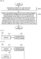
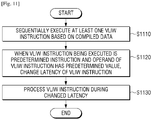
- FIG. 11 is a flowchart of a control method of a VLIW processor, according to an embodiment of the present disclosure.
- At least one VLIW instruction can first be sequentially executed based on the compiled data at step S1110. If the VLIW instruction being executed is the predetermined VLIW instruction, and the operand of the VLIW instruction has the predetermined value, the latency of the VLIW instruction is changed at step S1120. In addition, the VLIW instruction is processed during the changed latency at step S1130.
- the method may further include, when the multi-cycle nop instruction for the plurality of function units is identified within the cycle corresponding to the latency of the VLIW instruction, and the end cycle of the other VLIW instruction which is being currently executed is within the cycle corresponding to the latency of the VLIW instruction, shortening the cycle of the multi-cycle nop instruction based on the cycle difference between the end cycle of the VLIW instruction and the other VLIW cycle to process the compiled data using the plurality of function units.
- the other VLIW instruction is the VLIW instruction having the most cycles remaining until the execution completion among the VLIW instructions which are being currently executed.
- the method may also include storing information on a latency of the other VLIW instruction in the register included in the VLIW processor, e.g., during processing of the compiled data using the plurality of function units. If the end cycle of the other instruction is within the cycle corresponding to the latency of the VLIW instruction, based on the information stored in the register, the cycle of the multi-cycle nop instruction may be shortened based on the cycle difference to process the compiled data using the plurality of function units.
- the information on the latency of the other VLIW instruction stored in the register may include at least one of cycle identification information corresponding to the latency of the other VLIW instruction, and information on the number of cycles remaining until the execution completion of the other VLIW instruction based on a current cycle.
- the cycle of the multi-cycle nop instruction may be shortened based on the information on the cycle difference to process the compiled data, i.e., when the compiled data is being processed.
- the VLIW processor may improve data processing speed by shortening some cycles of the compiled data in which the VLIW instruction is compiled.
- the methods described above may be programmed and stored in a variety of storage mediums. Accordingly, the methods described herein may be implemented in various types of electronic devices that are capable of executing in one of the storage mediums.
- a non-transitory computer readable medium in which a program for sequentially performing the control method described above is stored may be provided.
- the non-transitory computer readable medium is not limited to a medium that permanently stores data therein, e.g., a register, a cache, a memory, or the like, but can be a medium that semi-permanently stores data therein and is readable by a device.
- the various applications or programs described above may be stored and provided in the non-transitory computer readable medium such as a compact disk (CD), a digital versatile disk (DVD), a hard disk, a Blu-ray disk, a universal serial bus (USB), a memory card, a read only memory (ROM), or other suitable storage mediums.
Landscapes
- Engineering & Computer Science (AREA)
- Theoretical Computer Science (AREA)
- Software Systems (AREA)
- General Engineering & Computer Science (AREA)
- Physics & Mathematics (AREA)
- General Physics & Mathematics (AREA)
- Computer Hardware Design (AREA)
- Advance Control (AREA)
- Executing Machine-Instructions (AREA)
- Devices For Executing Special Programs (AREA)
Claims (2)
- Elektronische Vorrichtung (100), die kompilierte Daten erzeugt, die in einem Prozessor (200) mit sehr langem Befehlswort VLIW verwendet werden, einschließlich einer Vielzahl von Funktionseinheiten, wobei die elektronische Vorrichtung (100) Folgendes umfasst:einen Speicher (110); undeinen Prozessor (120), der konfiguriert ist, um:den Speicher (110) zu steuern, um die kompilierten Daten zu speichern, in denen mehrere VLIW-Befehle kompiliert sind,einen vorbestimmten VLIW-Befehl aus den kompilierten Daten zu identifizieren; undwenn ein Mehrzyklus-Nicht-Betriebsbefehl nop für die Vielzahl von Funktionseinheiten innerhalb eines Zyklus identifiziert wird, der einer Latenz des identifizierten VLIW-Befehls entspricht,wenn sich ein Endzyklus eines anderen VLIW-Befehls innerhalb des Zyklus befindet, der der Latenz des identifizierten VLIW-Befehls entspricht, und wenn in den Zyklen zwischen dem Endzyklus des anderen VLIW-Befehls und dem Endzyklus des identifizierten VLIW-Befehls kein weiterer VLIW-Befehl identifiziert wird:eine Anzahl von Zyklen zu zählen, die einer Zyklusdifferenz zwischen einem Endzyklus des identifizierten VLIW-Befehls und dem Endzyklus des anderen VLIW-Befehls entsprechen; unddie kompilierten Daten durch Einfügen des gezählten Werts in einen Operationscode OP des Mehrzyklus-NOP-Befehls zu aktualisieren;wobei der andere VLIW-Befehl ein Befehl ist, der in einem der Zyklen enthalten ist, in denen der identifizierte VLIW-Befehl enthalten ist, und ein vorheriger Zyklus davon, wobei der andere VLIW-Befehl die meisten verbleibenden Zyklen bis zum Abschluss der Ausführung unter den VLIW-Befehlen aufweist, die derzeit ausgeführt werden würden.
- Elektronische Vorrichtung nach Anspruch 1, wobei der Prozessor (120) Identifikationsinformationen des identifizierten VLIW-Befehls und Identifikationsinformationen des in den kompilierten Daten enthaltenen Mehrzyklus-NOP-Befehls synchronisiert, wenn der Mehrzyklus-NOP-Befehl innerhalb des der Latenz des identifizierten VLIW-Befehls entsprechenden Zyklus identifiziert wird.
Applications Claiming Priority (2)
| Application Number | Priority Date | Filing Date | Title |
|---|---|---|---|
| KR1020160119489A KR102688577B1 (ko) | 2016-09-19 | 2016-09-19 | 전자 장치, vliw 프로세서 및 그 제어 방법들 |
| PCT/KR2017/009800 WO2018052218A1 (en) | 2016-09-19 | 2017-09-07 | Electronic apparatus, vliw processor and control methods thererof |
Publications (3)
| Publication Number | Publication Date |
|---|---|
| EP3485372A1 EP3485372A1 (de) | 2019-05-22 |
| EP3485372A4 EP3485372A4 (de) | 2019-11-06 |
| EP3485372B1 true EP3485372B1 (de) | 2020-11-04 |
Family
ID=61619616
Family Applications (1)
| Application Number | Title | Priority Date | Filing Date |
|---|---|---|---|
| EP17851092.1A Active EP3485372B1 (de) | 2016-09-19 | 2017-09-07 | Elektronische vorrichtung, vliw-prozessor und steuerungsverfahren dafür |
Country Status (4)
| Country | Link |
|---|---|
| US (1) | US10379866B2 (de) |
| EP (1) | EP3485372B1 (de) |
| KR (1) | KR102688577B1 (de) |
| WO (1) | WO2018052218A1 (de) |
Families Citing this family (3)
| Publication number | Priority date | Publication date | Assignee | Title |
|---|---|---|---|---|
| US12067395B2 (en) | 2021-08-12 | 2024-08-20 | Tenstorrent Inc. | Pre-staged instruction registers for variable length instruction set machine |
| US11599358B1 (en) | 2021-08-12 | 2023-03-07 | Tenstorrent Inc. | Pre-staged instruction registers for variable length instruction set machine |
| CN117950670A (zh) * | 2022-10-31 | 2024-04-30 | 华为技术有限公司 | 程序的编译方法及装置 |
Family Cites Families (22)
| Publication number | Priority date | Publication date | Assignee | Title |
|---|---|---|---|---|
| US5021985A (en) | 1990-01-19 | 1991-06-04 | Weitek Corporation | Variable latency method and apparatus for floating-point coprocessor |
| JP3499252B2 (ja) | 1993-03-19 | 2004-02-23 | 株式会社ルネサステクノロジ | コンパイル装置及びデータ処理装置 |
| KR970053069A (ko) | 1995-12-30 | 1997-07-29 | 김주용 | 모오스 전계 효과 트랜지스터 제조 방법 |
| JPH09265397A (ja) | 1996-03-29 | 1997-10-07 | Hitachi Ltd | Vliw命令用プロセッサ |
| US5958044A (en) * | 1997-01-24 | 1999-09-28 | Texas Instruments Incorporated | Multicycle NOP |
| KR19990032104A (ko) | 1997-10-16 | 1999-05-06 | 조영일 | 고속벡터처리용 마이크로컴퓨터의 벡터처리장치 |
| US5961630A (en) | 1997-12-30 | 1999-10-05 | Intel Corporation | Method and apparatus for handling dynamic structural hazards and exceptions by using post-ready latency |
| US6487575B1 (en) | 1998-08-31 | 2002-11-26 | Advanced Micro Devices, Inc. | Early completion of iterative division |
| JP3830683B2 (ja) * | 1998-12-28 | 2006-10-04 | 富士通株式会社 | Vliwプロセッサ |
| US6275929B1 (en) * | 1999-05-26 | 2001-08-14 | Infineon Technologies Ag L. Gr. | Delay-slot control mechanism for microprocessors |
| US6799266B1 (en) | 1999-12-30 | 2004-09-28 | Texas Instruments Incorporated | Methods and apparatus for reducing the size of code with an exposed pipeline by encoding NOP operations as instruction operands |
| JP3564445B2 (ja) | 2001-09-20 | 2004-09-08 | 松下電器産業株式会社 | プロセッサ、コンパイル装置及びコンパイル方法 |
| US7430654B2 (en) | 2003-07-09 | 2008-09-30 | Via Technologies, Inc. | Dynamic instruction dependency monitor and control system |
| KR20060123079A (ko) | 2003-08-28 | 2006-12-01 | 코닌클리즈케 필립스 일렉트로닉스 엔.브이. | 명령어 데이터 프로세싱에 대한 방법 및 마이크로컨트롤러구조 및 저장 매체 |
| US7284117B1 (en) | 2003-11-04 | 2007-10-16 | Advanced Micro Devices, Inc. | Processor that predicts floating point instruction latency based on predicted precision |
| JP2005149297A (ja) | 2003-11-18 | 2005-06-09 | Renesas Technology Corp | プロセッサおよびそのアセンブラ |
| GB2414308B (en) | 2004-05-17 | 2007-08-15 | Advanced Risc Mach Ltd | Program instruction compression |
| KR100875836B1 (ko) * | 2007-03-23 | 2008-12-24 | 삼성전자주식회사 | 병렬 처리 vliw 컴퓨터를 위한 인스트럭션 명령어 압축장치 및 그 방법 |
| US8631056B2 (en) * | 2008-01-09 | 2014-01-14 | Qualcomm Incorporated | Processor and method of determining a normalization count |
| US8255726B2 (en) * | 2008-07-18 | 2012-08-28 | International Business Machines Corporation | Zero indication forwarding for floating point unit power reduction |
| KR101603751B1 (ko) * | 2010-02-18 | 2016-03-16 | 삼성전자주식회사 | 명령어 병렬 처리 컴퓨터를 위한 명령어 압축 장치 및 방법 |
| KR102056730B1 (ko) | 2013-04-22 | 2019-12-17 | 삼성전자주식회사 | Vliw 프로세서를 위한 명령어 압축 장치 및 방법과, 명령어 인출 장치 및 방법 |
-
2016
- 2016-09-19 KR KR1020160119489A patent/KR102688577B1/ko active Active
-
2017
- 2017-07-19 US US15/654,277 patent/US10379866B2/en active Active
- 2017-09-07 WO PCT/KR2017/009800 patent/WO2018052218A1/en not_active Ceased
- 2017-09-07 EP EP17851092.1A patent/EP3485372B1/de active Active
Non-Patent Citations (1)
| Title |
|---|
| None * |
Also Published As
| Publication number | Publication date |
|---|---|
| KR20180031266A (ko) | 2018-03-28 |
| EP3485372A4 (de) | 2019-11-06 |
| US20180081692A1 (en) | 2018-03-22 |
| KR102688577B1 (ko) | 2024-07-26 |
| WO2018052218A1 (en) | 2018-03-22 |
| US10379866B2 (en) | 2019-08-13 |
| EP3485372A1 (de) | 2019-05-22 |
Similar Documents
| Publication | Publication Date | Title |
|---|---|---|
| JP5865405B2 (ja) | 命令の制御フローの追跡 | |
| US9639371B2 (en) | Solution to divergent branches in a SIMD core using hardware pointers | |
| US10534613B2 (en) | Supporting learned branch predictors | |
| JP6006247B2 (ja) | 共有メモリへのアクセスの同期を緩和するプロセッサ、方法、システム、及びプログラム | |
| US8332597B1 (en) | Synchronization of external memory accesses in a dataflow machine | |
| US9870225B2 (en) | Processor with virtualized instruction set architecture and methods | |
| JP6306729B2 (ja) | ストアをソート及びリタイアする命令及びロジック | |
| EP2951682B1 (de) | Hardware und softwarelösungen für divergierende abzweigungen in einer parallelen rohrleitung | |
| TWI715681B (zh) | 用於位元欄位位址和插入之指令及邏輯 | |
| CN112540794B (zh) | 处理器核、处理器、装置和指令处理方法 | |
| TWI721021B (zh) | 用於致能旗標操作的移除及重建之處理器、非暫時性機器可讀取媒體及計算系統 | |
| US11789734B2 (en) | Padded vectorization with compile time known masks | |
| US20150095627A1 (en) | Two level re-order buffer | |
| CN101593096B (zh) | 一种共享寄存器相关性消除的实现方法 | |
| CN110825437B (zh) | 用于处理数据的方法和装置 | |
| US10379866B2 (en) | Electronic apparatus, VLIW processor and control methods for updating a multi-cycle no operation (NOP) instruction | |
| US9384001B2 (en) | Custom chaining stubs for instruction code translation | |
| US20150227371A1 (en) | Processors with Support for Compact Branch Instructions & Methods | |
| CN120295673B (zh) | 一种基于risc-v的处理器与电子设备 | |
| CN105700855B (zh) | 用于改进simd knn实现的设备、方法、系统和机器可读介质 | |
| WO2023142524A1 (zh) | 指令处理方法、装置、芯片、电子设备以及存储介质 | |
| US8924693B2 (en) | Predicting a result for a predicate-generating instruction when processing vector instructions | |
| CN116507999A (zh) | 一种处理器、处理方法及相关设备 | |
| US10606602B2 (en) | Electronic apparatus, processor and control method including a compiler scheduling instructions to reduce unused input ports | |
| EP4453716A1 (de) | Multizyklusplaner mit spekulativer aufnahme von mikrooperationen |
Legal Events
| Date | Code | Title | Description |
|---|---|---|---|
| STAA | Information on the status of an ep patent application or granted ep patent |
Free format text: STATUS: THE INTERNATIONAL PUBLICATION HAS BEEN MADE |
|
| PUAI | Public reference made under article 153(3) epc to a published international application that has entered the european phase |
Free format text: ORIGINAL CODE: 0009012 |
|
| STAA | Information on the status of an ep patent application or granted ep patent |
Free format text: STATUS: REQUEST FOR EXAMINATION WAS MADE |
|
| 17P | Request for examination filed |
Effective date: 20190215 |
|
| AK | Designated contracting states |
Kind code of ref document: A1 Designated state(s): AL AT BE BG CH CY CZ DE DK EE ES FI FR GB GR HR HU IE IS IT LI LT LU LV MC MK MT NL NO PL PT RO RS SE SI SK SM TR |
|
| AX | Request for extension of the european patent |
Extension state: BA ME |
|
| RIC1 | Information provided on ipc code assigned before grant |
Ipc: G06F 9/38 20180101AFI20190618BHEP Ipc: G06F 8/41 20180101ALI20190618BHEP Ipc: G06F 9/30 20180101ALI20190618BHEP |
|
| A4 | Supplementary search report drawn up and despatched |
Effective date: 20191007 |
|
| RIC1 | Information provided on ipc code assigned before grant |
Ipc: G06F 8/41 20180101ALI20190930BHEP Ipc: G06F 9/38 20180101AFI20190930BHEP Ipc: G06F 9/30 20180101ALI20190930BHEP |
|
| DAV | Request for validation of the european patent (deleted) | ||
| DAX | Request for extension of the european patent (deleted) | ||
| STAA | Information on the status of an ep patent application or granted ep patent |
Free format text: STATUS: EXAMINATION IS IN PROGRESS |
|
| 17Q | First examination report despatched |
Effective date: 20200305 |
|
| GRAP | Despatch of communication of intention to grant a patent |
Free format text: ORIGINAL CODE: EPIDOSNIGR1 |
|
| STAA | Information on the status of an ep patent application or granted ep patent |
Free format text: STATUS: GRANT OF PATENT IS INTENDED |
|
| INTG | Intention to grant announced |
Effective date: 20200504 |
|
| GRAS | Grant fee paid |
Free format text: ORIGINAL CODE: EPIDOSNIGR3 |
|
| GRAA | (expected) grant |
Free format text: ORIGINAL CODE: 0009210 |
|
| STAA | Information on the status of an ep patent application or granted ep patent |
Free format text: STATUS: THE PATENT HAS BEEN GRANTED |
|
| AK | Designated contracting states |
Kind code of ref document: B1 Designated state(s): AL AT BE BG CH CY CZ DE DK EE ES FI FR GB GR HR HU IE IS IT LI LT LU LV MC MK MT NL NO PL PT RO RS SE SI SK SM TR |
|
| REG | Reference to a national code |
Ref country code: GB Ref legal event code: FG4D |
|
| REG | Reference to a national code |
Ref country code: CH Ref legal event code: EP |
|
| REG | Reference to a national code |
Ref country code: AT Ref legal event code: REF Ref document number: 1331682 Country of ref document: AT Kind code of ref document: T Effective date: 20201115 |
|
| REG | Reference to a national code |
Ref country code: IE Ref legal event code: FG4D |
|
| REG | Reference to a national code |
Ref country code: DE Ref legal event code: R096 Ref document number: 602017027122 Country of ref document: DE |
|
| REG | Reference to a national code |
Ref country code: NL Ref legal event code: MP Effective date: 20201104 |
|
| REG | Reference to a national code |
Ref country code: AT Ref legal event code: MK05 Ref document number: 1331682 Country of ref document: AT Kind code of ref document: T Effective date: 20201104 |
|
| PG25 | Lapsed in a contracting state [announced via postgrant information from national office to epo] |
Ref country code: GR Free format text: LAPSE BECAUSE OF FAILURE TO SUBMIT A TRANSLATION OF THE DESCRIPTION OR TO PAY THE FEE WITHIN THE PRESCRIBED TIME-LIMIT Effective date: 20210205 Ref country code: NO Free format text: LAPSE BECAUSE OF FAILURE TO SUBMIT A TRANSLATION OF THE DESCRIPTION OR TO PAY THE FEE WITHIN THE PRESCRIBED TIME-LIMIT Effective date: 20210204 Ref country code: PT Free format text: LAPSE BECAUSE OF FAILURE TO SUBMIT A TRANSLATION OF THE DESCRIPTION OR TO PAY THE FEE WITHIN THE PRESCRIBED TIME-LIMIT Effective date: 20210304 Ref country code: RS Free format text: LAPSE BECAUSE OF FAILURE TO SUBMIT A TRANSLATION OF THE DESCRIPTION OR TO PAY THE FEE WITHIN THE PRESCRIBED TIME-LIMIT Effective date: 20201104 Ref country code: FI Free format text: LAPSE BECAUSE OF FAILURE TO SUBMIT A TRANSLATION OF THE DESCRIPTION OR TO PAY THE FEE WITHIN THE PRESCRIBED TIME-LIMIT Effective date: 20201104 |
|
| PG25 | Lapsed in a contracting state [announced via postgrant information from national office to epo] |
Ref country code: BG Free format text: LAPSE BECAUSE OF FAILURE TO SUBMIT A TRANSLATION OF THE DESCRIPTION OR TO PAY THE FEE WITHIN THE PRESCRIBED TIME-LIMIT Effective date: 20210204 Ref country code: SE Free format text: LAPSE BECAUSE OF FAILURE TO SUBMIT A TRANSLATION OF THE DESCRIPTION OR TO PAY THE FEE WITHIN THE PRESCRIBED TIME-LIMIT Effective date: 20201104 Ref country code: IS Free format text: LAPSE BECAUSE OF FAILURE TO SUBMIT A TRANSLATION OF THE DESCRIPTION OR TO PAY THE FEE WITHIN THE PRESCRIBED TIME-LIMIT Effective date: 20210304 Ref country code: PL Free format text: LAPSE BECAUSE OF FAILURE TO SUBMIT A TRANSLATION OF THE DESCRIPTION OR TO PAY THE FEE WITHIN THE PRESCRIBED TIME-LIMIT Effective date: 20201104 Ref country code: LV Free format text: LAPSE BECAUSE OF FAILURE TO SUBMIT A TRANSLATION OF THE DESCRIPTION OR TO PAY THE FEE WITHIN THE PRESCRIBED TIME-LIMIT Effective date: 20201104 Ref country code: AT Free format text: LAPSE BECAUSE OF FAILURE TO SUBMIT A TRANSLATION OF THE DESCRIPTION OR TO PAY THE FEE WITHIN THE PRESCRIBED TIME-LIMIT Effective date: 20201104 Ref country code: ES Free format text: LAPSE BECAUSE OF FAILURE TO SUBMIT A TRANSLATION OF THE DESCRIPTION OR TO PAY THE FEE WITHIN THE PRESCRIBED TIME-LIMIT Effective date: 20201104 |
|
| REG | Reference to a national code |
Ref country code: LT Ref legal event code: MG9D |
|
| PG25 | Lapsed in a contracting state [announced via postgrant information from national office to epo] |
Ref country code: HR Free format text: LAPSE BECAUSE OF FAILURE TO SUBMIT A TRANSLATION OF THE DESCRIPTION OR TO PAY THE FEE WITHIN THE PRESCRIBED TIME-LIMIT Effective date: 20201104 |
|
| PG25 | Lapsed in a contracting state [announced via postgrant information from national office to epo] |
Ref country code: SK Free format text: LAPSE BECAUSE OF FAILURE TO SUBMIT A TRANSLATION OF THE DESCRIPTION OR TO PAY THE FEE WITHIN THE PRESCRIBED TIME-LIMIT Effective date: 20201104 Ref country code: RO Free format text: LAPSE BECAUSE OF FAILURE TO SUBMIT A TRANSLATION OF THE DESCRIPTION OR TO PAY THE FEE WITHIN THE PRESCRIBED TIME-LIMIT Effective date: 20201104 Ref country code: SM Free format text: LAPSE BECAUSE OF FAILURE TO SUBMIT A TRANSLATION OF THE DESCRIPTION OR TO PAY THE FEE WITHIN THE PRESCRIBED TIME-LIMIT Effective date: 20201104 Ref country code: EE Free format text: LAPSE BECAUSE OF FAILURE TO SUBMIT A TRANSLATION OF THE DESCRIPTION OR TO PAY THE FEE WITHIN THE PRESCRIBED TIME-LIMIT Effective date: 20201104 Ref country code: CZ Free format text: LAPSE BECAUSE OF FAILURE TO SUBMIT A TRANSLATION OF THE DESCRIPTION OR TO PAY THE FEE WITHIN THE PRESCRIBED TIME-LIMIT Effective date: 20201104 Ref country code: LT Free format text: LAPSE BECAUSE OF FAILURE TO SUBMIT A TRANSLATION OF THE DESCRIPTION OR TO PAY THE FEE WITHIN THE PRESCRIBED TIME-LIMIT Effective date: 20201104 |
|
| REG | Reference to a national code |
Ref country code: DE Ref legal event code: R097 Ref document number: 602017027122 Country of ref document: DE |
|
| PG25 | Lapsed in a contracting state [announced via postgrant information from national office to epo] |
Ref country code: DK Free format text: LAPSE BECAUSE OF FAILURE TO SUBMIT A TRANSLATION OF THE DESCRIPTION OR TO PAY THE FEE WITHIN THE PRESCRIBED TIME-LIMIT Effective date: 20201104 |
|
| PLBE | No opposition filed within time limit |
Free format text: ORIGINAL CODE: 0009261 |
|
| STAA | Information on the status of an ep patent application or granted ep patent |
Free format text: STATUS: NO OPPOSITION FILED WITHIN TIME LIMIT |
|
| 26N | No opposition filed |
Effective date: 20210805 |
|
| PG25 | Lapsed in a contracting state [announced via postgrant information from national office to epo] |
Ref country code: AL Free format text: LAPSE BECAUSE OF FAILURE TO SUBMIT A TRANSLATION OF THE DESCRIPTION OR TO PAY THE FEE WITHIN THE PRESCRIBED TIME-LIMIT Effective date: 20201104 Ref country code: NL Free format text: LAPSE BECAUSE OF FAILURE TO SUBMIT A TRANSLATION OF THE DESCRIPTION OR TO PAY THE FEE WITHIN THE PRESCRIBED TIME-LIMIT Effective date: 20201104 Ref country code: IT Free format text: LAPSE BECAUSE OF FAILURE TO SUBMIT A TRANSLATION OF THE DESCRIPTION OR TO PAY THE FEE WITHIN THE PRESCRIBED TIME-LIMIT Effective date: 20201104 |
|
| PG25 | Lapsed in a contracting state [announced via postgrant information from national office to epo] |
Ref country code: SI Free format text: LAPSE BECAUSE OF FAILURE TO SUBMIT A TRANSLATION OF THE DESCRIPTION OR TO PAY THE FEE WITHIN THE PRESCRIBED TIME-LIMIT Effective date: 20201104 |
|
| REG | Reference to a national code |
Ref country code: CH Ref legal event code: PL |
|
| REG | Reference to a national code |
Ref country code: BE Ref legal event code: MM Effective date: 20210930 |
|
| PG25 | Lapsed in a contracting state [announced via postgrant information from national office to epo] |
Ref country code: IS Free format text: LAPSE BECAUSE OF FAILURE TO SUBMIT A TRANSLATION OF THE DESCRIPTION OR TO PAY THE FEE WITHIN THE PRESCRIBED TIME-LIMIT Effective date: 20210304 Ref country code: MC Free format text: LAPSE BECAUSE OF FAILURE TO SUBMIT A TRANSLATION OF THE DESCRIPTION OR TO PAY THE FEE WITHIN THE PRESCRIBED TIME-LIMIT Effective date: 20201104 |
|
| PG25 | Lapsed in a contracting state [announced via postgrant information from national office to epo] |
Ref country code: LU Free format text: LAPSE BECAUSE OF NON-PAYMENT OF DUE FEES Effective date: 20210907 Ref country code: IE Free format text: LAPSE BECAUSE OF NON-PAYMENT OF DUE FEES Effective date: 20210907 Ref country code: FR Free format text: LAPSE BECAUSE OF NON-PAYMENT OF DUE FEES Effective date: 20210930 Ref country code: BE Free format text: LAPSE BECAUSE OF NON-PAYMENT OF DUE FEES Effective date: 20210930 |
|
| PG25 | Lapsed in a contracting state [announced via postgrant information from national office to epo] |
Ref country code: LI Free format text: LAPSE BECAUSE OF NON-PAYMENT OF DUE FEES Effective date: 20210930 Ref country code: CH Free format text: LAPSE BECAUSE OF NON-PAYMENT OF DUE FEES Effective date: 20210930 |
|
| PG25 | Lapsed in a contracting state [announced via postgrant information from national office to epo] |
Ref country code: CY Free format text: LAPSE BECAUSE OF FAILURE TO SUBMIT A TRANSLATION OF THE DESCRIPTION OR TO PAY THE FEE WITHIN THE PRESCRIBED TIME-LIMIT Effective date: 20201104 |
|
| PG25 | Lapsed in a contracting state [announced via postgrant information from national office to epo] |
Ref country code: HU Free format text: LAPSE BECAUSE OF FAILURE TO SUBMIT A TRANSLATION OF THE DESCRIPTION OR TO PAY THE FEE WITHIN THE PRESCRIBED TIME-LIMIT; INVALID AB INITIO Effective date: 20170907 |
|
| PG25 | Lapsed in a contracting state [announced via postgrant information from national office to epo] |
Ref country code: MK Free format text: LAPSE BECAUSE OF FAILURE TO SUBMIT A TRANSLATION OF THE DESCRIPTION OR TO PAY THE FEE WITHIN THE PRESCRIBED TIME-LIMIT Effective date: 20201104 |
|
| PG25 | Lapsed in a contracting state [announced via postgrant information from national office to epo] |
Ref country code: MT Free format text: LAPSE BECAUSE OF FAILURE TO SUBMIT A TRANSLATION OF THE DESCRIPTION OR TO PAY THE FEE WITHIN THE PRESCRIBED TIME-LIMIT Effective date: 20201104 |
|
| PGFP | Annual fee paid to national office [announced via postgrant information from national office to epo] |
Ref country code: DE Payment date: 20250820 Year of fee payment: 9 |
|
| PGFP | Annual fee paid to national office [announced via postgrant information from national office to epo] |
Ref country code: GB Payment date: 20250820 Year of fee payment: 9 |
|
| PG25 | Lapsed in a contracting state [announced via postgrant information from national office to epo] |
Ref country code: TR Free format text: LAPSE BECAUSE OF FAILURE TO SUBMIT A TRANSLATION OF THE DESCRIPTION OR TO PAY THE FEE WITHIN THE PRESCRIBED TIME-LIMIT Effective date: 20201104 |