EP3482868A2 - Apparatus for manufacturing a mask and method for manufacturing a mask - Google Patents
Apparatus for manufacturing a mask and method for manufacturing a mask Download PDFInfo
- Publication number
- EP3482868A2 EP3482868A2 EP18206324.8A EP18206324A EP3482868A2 EP 3482868 A2 EP3482868 A2 EP 3482868A2 EP 18206324 A EP18206324 A EP 18206324A EP 3482868 A2 EP3482868 A2 EP 3482868A2
- Authority
- EP
- European Patent Office
- Prior art keywords
- mask
- laser beam
- shape
- pattern groove
- pattern
- Prior art date
- Legal status (The legal status is an assumption and is not a legal conclusion. Google has not performed a legal analysis and makes no representation as to the accuracy of the status listed.)
- Withdrawn
Links
Images





Classifications
-
- H—ELECTRICITY
- H10—SEMICONDUCTOR DEVICES; ELECTRIC SOLID-STATE DEVICES NOT OTHERWISE PROVIDED FOR
- H10K—ORGANIC ELECTRIC SOLID-STATE DEVICES
- H10K71/00—Manufacture or treatment specially adapted for the organic devices covered by this subclass
-
- B—PERFORMING OPERATIONS; TRANSPORTING
- B23—MACHINE TOOLS; METAL-WORKING NOT OTHERWISE PROVIDED FOR
- B23K—SOLDERING OR UNSOLDERING; WELDING; CLADDING OR PLATING BY SOLDERING OR WELDING; CUTTING BY APPLYING HEAT LOCALLY, e.g. FLAME CUTTING; WORKING BY LASER BEAM
- B23K26/00—Working by laser beam, e.g. welding, cutting or boring
- B23K26/02—Positioning or observing the workpiece, e.g. with respect to the point of impact; Aligning, aiming or focusing the laser beam
- B23K26/06—Shaping the laser beam, e.g. by masks or multi-focusing
- B23K26/062—Shaping the laser beam, e.g. by masks or multi-focusing by direct control of the laser beam
- B23K26/0622—Shaping the laser beam, e.g. by masks or multi-focusing by direct control of the laser beam by shaping pulses
- B23K26/0624—Shaping the laser beam, e.g. by masks or multi-focusing by direct control of the laser beam by shaping pulses using ultrashort pulses, i.e. pulses of 1 ns or less
-
- B—PERFORMING OPERATIONS; TRANSPORTING
- B23—MACHINE TOOLS; METAL-WORKING NOT OTHERWISE PROVIDED FOR
- B23K—SOLDERING OR UNSOLDERING; WELDING; CLADDING OR PLATING BY SOLDERING OR WELDING; CUTTING BY APPLYING HEAT LOCALLY, e.g. FLAME CUTTING; WORKING BY LASER BEAM
- B23K26/00—Working by laser beam, e.g. welding, cutting or boring
- B23K26/02—Positioning or observing the workpiece, e.g. with respect to the point of impact; Aligning, aiming or focusing the laser beam
- B23K26/06—Shaping the laser beam, e.g. by masks or multi-focusing
- B23K26/064—Shaping the laser beam, e.g. by masks or multi-focusing by means of optical elements, e.g. lenses, mirrors or prisms
-
- B—PERFORMING OPERATIONS; TRANSPORTING
- B23—MACHINE TOOLS; METAL-WORKING NOT OTHERWISE PROVIDED FOR
- B23K—SOLDERING OR UNSOLDERING; WELDING; CLADDING OR PLATING BY SOLDERING OR WELDING; CUTTING BY APPLYING HEAT LOCALLY, e.g. FLAME CUTTING; WORKING BY LASER BEAM
- B23K26/00—Working by laser beam, e.g. welding, cutting or boring
- B23K26/08—Devices involving relative movement between laser beam and workpiece
- B23K26/082—Scanning systems, i.e. devices involving movement of the laser beam relative to the laser head
-
- B—PERFORMING OPERATIONS; TRANSPORTING
- B23—MACHINE TOOLS; METAL-WORKING NOT OTHERWISE PROVIDED FOR
- B23K—SOLDERING OR UNSOLDERING; WELDING; CLADDING OR PLATING BY SOLDERING OR WELDING; CUTTING BY APPLYING HEAT LOCALLY, e.g. FLAME CUTTING; WORKING BY LASER BEAM
- B23K26/00—Working by laser beam, e.g. welding, cutting or boring
- B23K26/36—Removing material
- B23K26/362—Laser etching
-
- B—PERFORMING OPERATIONS; TRANSPORTING
- B23—MACHINE TOOLS; METAL-WORKING NOT OTHERWISE PROVIDED FOR
- B23K—SOLDERING OR UNSOLDERING; WELDING; CLADDING OR PLATING BY SOLDERING OR WELDING; CUTTING BY APPLYING HEAT LOCALLY, e.g. FLAME CUTTING; WORKING BY LASER BEAM
- B23K26/00—Working by laser beam, e.g. welding, cutting or boring
- B23K26/36—Removing material
- B23K26/362—Laser etching
- B23K26/364—Laser etching for making a groove or trench, e.g. for scribing a break initiation groove
-
- C—CHEMISTRY; METALLURGY
- C23—COATING METALLIC MATERIAL; COATING MATERIAL WITH METALLIC MATERIAL; CHEMICAL SURFACE TREATMENT; DIFFUSION TREATMENT OF METALLIC MATERIAL; COATING BY VACUUM EVAPORATION, BY SPUTTERING, BY ION IMPLANTATION OR BY CHEMICAL VAPOUR DEPOSITION, IN GENERAL; INHIBITING CORROSION OF METALLIC MATERIAL OR INCRUSTATION IN GENERAL
- C23C—COATING METALLIC MATERIAL; COATING MATERIAL WITH METALLIC MATERIAL; SURFACE TREATMENT OF METALLIC MATERIAL BY DIFFUSION INTO THE SURFACE, BY CHEMICAL CONVERSION OR SUBSTITUTION; COATING BY VACUUM EVAPORATION, BY SPUTTERING, BY ION IMPLANTATION OR BY CHEMICAL VAPOUR DEPOSITION, IN GENERAL
- C23C14/00—Coating by vacuum evaporation, by sputtering or by ion implantation of the coating forming material
- C23C14/04—Coating on selected surface areas, e.g. using masks
- C23C14/042—Coating on selected surface areas, e.g. using masks using masks
-
- C—CHEMISTRY; METALLURGY
- C23—COATING METALLIC MATERIAL; COATING MATERIAL WITH METALLIC MATERIAL; CHEMICAL SURFACE TREATMENT; DIFFUSION TREATMENT OF METALLIC MATERIAL; COATING BY VACUUM EVAPORATION, BY SPUTTERING, BY ION IMPLANTATION OR BY CHEMICAL VAPOUR DEPOSITION, IN GENERAL; INHIBITING CORROSION OF METALLIC MATERIAL OR INCRUSTATION IN GENERAL
- C23C—COATING METALLIC MATERIAL; COATING MATERIAL WITH METALLIC MATERIAL; SURFACE TREATMENT OF METALLIC MATERIAL BY DIFFUSION INTO THE SURFACE, BY CHEMICAL CONVERSION OR SUBSTITUTION; COATING BY VACUUM EVAPORATION, BY SPUTTERING, BY ION IMPLANTATION OR BY CHEMICAL VAPOUR DEPOSITION, IN GENERAL
- C23C16/00—Chemical coating by decomposition of gaseous compounds, without leaving reaction products of surface material in the coating, i.e. chemical vapour deposition [CVD] processes
- C23C16/04—Coating on selected surface areas, e.g. using masks
- C23C16/042—Coating on selected surface areas, e.g. using masks using masks
-
- H—ELECTRICITY
- H10—SEMICONDUCTOR DEVICES; ELECTRIC SOLID-STATE DEVICES NOT OTHERWISE PROVIDED FOR
- H10K—ORGANIC ELECTRIC SOLID-STATE DEVICES
- H10K71/00—Manufacture or treatment specially adapted for the organic devices covered by this subclass
- H10K71/10—Deposition of organic active material
- H10K71/16—Deposition of organic active material using physical vapour deposition [PVD], e.g. vacuum deposition or sputtering
- H10K71/164—Deposition of organic active material using physical vapour deposition [PVD], e.g. vacuum deposition or sputtering using vacuum deposition
-
- H—ELECTRICITY
- H10—SEMICONDUCTOR DEVICES; ELECTRIC SOLID-STATE DEVICES NOT OTHERWISE PROVIDED FOR
- H10K—ORGANIC ELECTRIC SOLID-STATE DEVICES
- H10K71/00—Manufacture or treatment specially adapted for the organic devices covered by this subclass
- H10K71/10—Deposition of organic active material
- H10K71/16—Deposition of organic active material using physical vapour deposition [PVD], e.g. vacuum deposition or sputtering
- H10K71/166—Deposition of organic active material using physical vapour deposition [PVD], e.g. vacuum deposition or sputtering using selective deposition, e.g. using a mask
-
- H—ELECTRICITY
- H10—SEMICONDUCTOR DEVICES; ELECTRIC SOLID-STATE DEVICES NOT OTHERWISE PROVIDED FOR
- H10P—GENERIC PROCESSES OR APPARATUS FOR THE MANUFACTURE OR TREATMENT OF DEVICES COVERED BY CLASS H10
- H10P76/00—Manufacture or treatment of masks on semiconductor bodies, e.g. by lithography or photolithography
- H10P76/40—Manufacture or treatment of masks on semiconductor bodies, e.g. by lithography or photolithography of masks comprising inorganic materials
- H10P76/408—Manufacture or treatment of masks on semiconductor bodies, e.g. by lithography or photolithography of masks comprising inorganic materials characterised by their sizes, orientations, dispositions, behaviours or shapes
- H10P76/4085—Manufacture or treatment of masks on semiconductor bodies, e.g. by lithography or photolithography of masks comprising inorganic materials characterised by their sizes, orientations, dispositions, behaviours or shapes characterised by the processes involved to create the masks
-
- B—PERFORMING OPERATIONS; TRANSPORTING
- B23—MACHINE TOOLS; METAL-WORKING NOT OTHERWISE PROVIDED FOR
- B23K—SOLDERING OR UNSOLDERING; WELDING; CLADDING OR PLATING BY SOLDERING OR WELDING; CUTTING BY APPLYING HEAT LOCALLY, e.g. FLAME CUTTING; WORKING BY LASER BEAM
- B23K2103/00—Materials to be soldered, welded or cut
- B23K2103/02—Iron or ferrous alloys
-
- H—ELECTRICITY
- H10—SEMICONDUCTOR DEVICES; ELECTRIC SOLID-STATE DEVICES NOT OTHERWISE PROVIDED FOR
- H10K—ORGANIC ELECTRIC SOLID-STATE DEVICES
- H10K59/00—Integrated devices, or assemblies of multiple devices, comprising at least one organic light-emitting element covered by group H10K50/00
- H10K59/10—OLED displays
- H10K59/12—Active-matrix OLED [AMOLED] displays
Definitions
- the present disclosure herein relates to an apparatus for manufacturing a mask and a method for manufacturing a mask.
- Display devices output a video or an image using pixels that have pixel areas, so as to provide various kinds of visual information to a user.
- Organic light emitting display devices of the display devices have a wide viewing angle, excellent contrast, and fast response speed.
- the formation of the Pixel areas of these organic light emitting display devices may employ a deposition process to deposit a deposition material.
- an organic material is deposited on a substrate through a fine metal mask (FMM) to provide a thin film having a desired pattern.
- FMM fine metal mask
- an opening of a mask through which the deposition material is transferred also requires a precise manufacturing process.
- the opening may be made by etching one surface and the other surface of the mask so as to provide a precise opening, but a protrusion is made during the etching process of the both surfaces, which causes the shadow effect that makes it impossible to perform the deposition of the desired shape and size during the deposition process.
- An aspect of the present disclosure relates to an apparatus for manufacturing a mask, so as to provide a mask for solving the above-described limitation.
- An aspect of the present disclosure provides an apparatus for manufacturing a mask, which enables a more precise deposition.
- An embodiment of the inventive concept provides an apparatus for manufacturing a mask, the apparatus including a stage on which a pre-mask is disposed such that a front surface of the pre-mask faces the stage (e.g., faces downward), and a laser irradiation device including a laser generation member configured to irradiate a laser beam to melt or remove a portion of the pre-mask, an optical system configured to receive the laser beam and control a shape of the laser beam, and a scanner configured to adjust a path of the laser beam that has the shape controlled by the optical system, .
- the pre-mask includes a first portion having a first pattern groove provided through the front surface and a second portion having a second pattern groove provided through a rear surface that faces oppositely away from the front surface, and the first portion and the second portion are arranged in a first direction that is a thickness direction of the pre-mask, and the laser beam with the controlled shape is irradiated onto the second portion of the pre-mask while being steered in a second direction crossing the first direction to remove the second portion to provide a mask having an opening.
- a width of the first pattern groove is greater than a width of the second pattern groove.
- the width of the first pattern groove has a maximum width ranging from about 15 ⁇ m to about 40 ⁇ m.
- the first pattern groove and the second pattern groove respectively, have widths that decrease gradually from the front surface and the rear surface of the pre-mask in the thickness direction of the pre-mask.
- a surface of the mask exposed by removing the second portion has an uneven surface shape.
- the laser beam may be a femto-second laser.
- the laser beam with the controlled shape may have a flat-top shape.
- the scanner may include a first mirror configured to reflect the laser beam with the controlled shape, a first driving part configured to rotate the first mirror, a second mirror configured to transmit the laser beam with the controlled shape, which is reflected from the first mirror, to the pre-mask, a second driving part configured to rotate the second mirror, and a lens configured to collect the laser beam with the controlled shape, which is reflected from the second mirror.
- a shape of an inner surface on a cross-section of each of the first pattern groove and the second pattern groove is formed of either a curved line or a straight line.
- an apparatus for manufacturing a mask includes: a stage on which a pre-mask is disposed, the pre-mask having a first surface and a second surface that face oppositely away from each other; and a laser irradiation device including a laser generation member configured to irradiate a laser beam to melt or remove a portion of the pre-mask, an optical system configured to receive the laser beam and control a shape of the laser beam, and a scanner configured to adjust a path of the laser beam that has the shape controlled by the optical system.
- the pre-mask has a first thickness
- the pre-mask includes a pattern portion having a protrusion, the pattern portion being provided in a first direction that is a thickness direction of the pre-mask
- the laser beam with the controlled shape is irradiated on any one of the first surface and the second surface of the pre-mask to provide a mask having a second thickness different from the first thickness and having an opening in which the protrusion is removed.
- the first thickness may be greater than the second thickness.
- the width of the opening may have a maximum width ranging from about 15 ⁇ m to about 40 ⁇ m.
- a shape of an inner surface of the pattern portion on a cross-section is formed of either a curved line or a straight line.
- a radius of curvature may decrease gradually from each of the first surface and the second surface of the mask toward the protrusion.
- a surface of the mask -- exposed by removing the protrusion -- has an uneven surface shape.
- the laser beam may be a femto-second laser beam.
- the laser beam with the controlled shape may have a flat-top shape.
- the scanner may include a first mirror configured to reflect the laser beam with the controlled shape, a first driving part configured to rotate the first mirror, a second mirror configured to transmit the laser beam with the controlled shape, which is reflected from the first mirror, to the mask, a second driving part configured to rotate the second mirror, and a lens configured to collect the laser beam with the controlled shape, which is reflected from the second mirror.
- a method for manufacturing a mask includes performing a first etching in which, for a pre-mask having a first surface and a second surface that face oppositely away from each other, a first pattern groove having a first depth is provided through the first surface, performing a second etching in which a second pattern groove having a second depth is provided through the second surface; and providing a mask that has a front surface having an even surface shape and a rear surface having an uneven surface shape, by removing any one of the first surface and the second surface of the pre-mask, wherein the rear surface is defined by removing any one of the first surface and the second surface.
- the providing of the mask may include irradiating a laser beam onto the front surface of the pre-mask and removing any one of the first surface and the second surface of the pre-mask.
- first and second are used herein to describe various elements, these elements should not be limited by these terms. Terms are only used to distinguish one component from other components. For example, a first element can be referred to as a second element, and similarly a second element can be referred to as a first element without departing from the scope of the present disclosure.
- the terms of a singular form may include plural forms unless definitely indicating a particular case in terms of the context.
- spatially relative terms such as “beneath”, “below”, “lower”, “under”, “above”, “upper” and the like, may be used herein for ease of description to describe one element or feature's relationship to another element(s) or feature(s) as illustrated in the figures. It will be understood that the spatially relative terms are intended to encompass different orientations of the device in use or in operation, in addition to the orientation depicted in the figures. For example, if the device in the figures is turned over, elements described as “below” or “beneath” or “under” other elements or features would then be oriented “above” the other elements or features. Thus, the example terms “below” and “under” can encompass both an orientation of above and below.
- the device may be otherwise oriented (e.g., rotated 90 degrees or at other orientations) and the spatially relative descriptors used herein should be interpreted accordingly.
- a layer when referred to as being "between" two layers, it can be the only layer between the two layers, or one or more intervening layers may also be present.
- any numerical range recited herein is intended to include all sub-ranges of the same numerical precision subsumed within the recited range.
- a range of "1.0 to 10.0” is intended to include all subranges between (and including) the recited minimum value of 1.0 and the recited maximum value of 10.0, that is, having a minimum value equal to or greater than 1.0 and a maximum value equal to or less than 10.0, such as, for example, 2.4 to 7.6.
- FIG. 1 is a schematic view of deposition equipment using a mask according to an embodiment of the inventive concept.
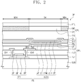
- FIG. 2 is a cross-sectional view illustrating a portion of a pixel area in a substrate according to an embodiment of the inventive concept. Referring to FIGS. 1 and 2 , a mask and a display substrate provided by the mask will be described in more detail.
- Deposition equipment 1000 includes a chamber 100, a substrate seat 200, a substrate 300, a mask frame 400, a deposition source 500, and a mask MS.
- the deposition equipment 1000 is used to provide a plurality of thin film patterns, which are included in a display device, on the substrate 300.
- a space may be defined therein.
- the substrate seat 200, the substrate 300, the mask frame 400, the deposition source 500, and the mask MS may be disposed within the inner space.
- an opening PO may be provided, and the opening PO corresponds to an area through which a deposition material DM is transferred.
- the substrate 300 is disposed on (e.g., under) the substrate seat 200, and the substrate seat 200 supports the substrate 300.
- the substrate seat 200 may be provided in various forms as long as it has a general structure capable of supporting the substrate 300.
- the substrate seat 300 may include a shuttle, an electrostatic chuck, or the like, which is disposed within the chamber 100.
- the deposition material DM is deposited on the substrate 300 through the opening PO of the mask MS, and an area deposited with the deposition material DM may be defined as a pixel area DA that emits light.
- a non-pixel area NDA may be defined between adjacent pixel areas.
- the mask frame 400 may be made of metal with high strength. Accordingly, the deformation of the mask frame 400, which may occur during welding, may be reduced, and thus a process may be stably performed, and a lifespan of the mask frame 400 may be increased.
- a welded portion in which the mask frame 400 and the mask MS are welded and coupled, may be formed.
- a high temperature is generated around this welded portion, and thus the mask frame 400 may be made of a material having the low thermal deformation.
- the deposition source 500 provides the deposition material DM to the substrate.
- the deposition source 500 may be provided with a set or predetermined inner space so as to accommodate the deposition material DM.
- the deposition material may be a material to be sublimated or vaporized, and include at least one of an inorganic substance, metal, or an organic substance.
- a suctioning or vacuum part is operated after the chamber 100 is closed, and thus may maintain the pressure inside the chamber 100 in a substantially vacuum state.
- the deposition source 500 may make the deposition material DM vaporized or sublimated, and accordingly, the deposition material DM passes through the mask MS and may be deposited on the substrate 300.
- the deposition material passes through the opening PO in the mask MS, and thus may be deposited, on the substrate, in a regular pattern.
- the deposition material DM is transferred through the mask MS and deposited on the substrate 300, and thus a deposition pattern EML is defined.
- the shape of the deposition pattern EML may correspond to the opening PO.
- the deposition pattern EML may be a light emitting pattern EML, which will be described later.
- the deposition material DM may include a light emitting material. However, this is merely described as an example.
- the deposition pattern EML may be various suitable patterns that constitute a display panel DP that will be described later, and is not limited to one embodiment.
- the display panel DP includes a display layer DPL, a thin film encapsulation layer TFE, a color filter layer CFL, and a protection layer PTL.
- the display layer DPL includes a base layer SUB, a pixel PX, and a plurality of insulation layers IL1, IL2, and IL3.
- the pixel PX includes a thin film transistor TFT and an organic light emitting element OLED.
- the first insulation layer IL1 and a semiconductor pattern AL of the thin film transistor TFT are disposed on the base layer SUB.
- the first insulation layer IL1 covers the semiconductor pattern AL.
- the second insulation layer IL2 and a control (e.g., gate) electrode GE of the thin film transistor TFT are disposed on the first insulation layer IL1.
- the second insulation layer IL2 covers the control electrode GE.
- Each of the first insulation layer IL1 and the second insulation layer IL2 includes an organic film and/or an inorganic film.
- Each of the first insulation layer IL1 and the second insulation layer IL2 may include a plurality of thin films.
- the third insulation layer IL3, and input and output (e.g., source and drain) electrodes SE and DE of the thin film transistor TFT are disposed on the second insulation layer IL2.
- the third insulation layer IL3 covers the input and output electrodes SE and DE.
- the input and output electrodes SE and DE are connected to the semiconductor pattern AL through first and second through-holes CH1 and CH2, which penetrate the first and second insulation layers IL1 and IL2, respectively.
- a layer, in which the control electrode GE, the input electrode SE, the output electrode DE, and the semiconductor pattern AL are disposed, may be diversely or suitably changed.
- the control electrode GE, the input electrode SE, and the output electrode DE may directly contact the semiconductor AL without a separate through-hole.
- Thin film transistor TFT according to an embodiment of the inventive concept may be provided in various structures, and is not limited to any one embodiment.
- the organic light emitting element OLED and a pixel defining film PDL are disposed on the third insulation layer IL3.
- the organic light emitting element OLED includes an anode electrode AE, a light emitting pattern EML, a cathode electrode CE, a hole transport region CL1 defined between the anode electrode AE and the light emitting pattern EML, and an electron transport region CL2 defined between the light emitting pattern EML and the cathode electrode CE.
- the anode electrode AE is provided in plurality, and each may be disposed to overlap a corresponding one of the pixel areas (along a thickness direction of the display panel DP).
- the pixel defining film PDL is disposed on the anode electrode AE, and exposes a portion of the anode electrode AE.
- the pixel defining film PDL substantially defines the pixel area DA.
- the anode electrode AE is connected to the output electrode DE through a third through-hole CH3 defined in the third insulation layer IL3.
- the hole transport region CL1 is disposed on the anode electrode AE, and covers the anode electrode AE and the pixel defining film PDL.
- the hole transport region CL1 may include at least any one of a hole injection layer, a hole transport layer, or a single layer having both a hole injecting function and a hole transporting function.
- the light emitting pattern EML is disposed on the hole transport region CL1.
- the light emitting pattern EML is provided in plurality, and each overlaps a corresponding one of light emitting areas (along a thickness direction of the display panel DP).
- the light emitting pattern EML may include a phosphorescent material and a fluorescent material.
- the light emitting pattern EML may generate light having one color, or light in which two or more colors are mixed.
- the substrate 300 provided to the deposition equipment 1000 may be supplied in a state in which layers up to the hole transport region CL1, which is a portion of the display layer DPL, are laminated.
- a lamination configuration of the substrate 300 provided to the deposition equipment 1000 is not limited to any one example.
- the electron transport region CL2 is disposed on the light emitting pattern EML, and covers the light emitting pattern EML and the hole transport region CL1.
- the electron transport region CL2 may include at least any one of an electron transport material or an electron injection material.
- the electron transport region CL2 may be an electron transport layer having the electron transport material, or an electron injection/transport single layer having the electron transport material and the electron injection material.
- the cathode electrode CE is disposed on the electron transport region CL2, and faces the anode electrode AE.
- the cathode electrode CE may be made of a material having a low work function so as to enable easy electron injection.
- the cathode electrode CE and the anode AE may be made of different materials, depending on a light emitting method.
- the cathode electrode CE may be a transmissive electrode
- the anode electrode AE may be a reflective electrode.
- the cathode electrode CE may be a reflective electrode
- the anode electrode AE may be a transmissive electrode.
- positions of the cathode electrode CE and the anode electrode AE are not limited thereto, and may be suitably changed.
- the pixel area DA according to the inventive concept may include organic light emitting elements having various suitable structures, and are not limited to any one embodiment.
- the thin film encapsulation layer TFE is disposed on the cathode electrode CE.
- the thin film encapsulation layer TFE covers an entire surface of the cathode electrode CE, and encapsulates the organic light emitting element OLED.
- the thin film encapsulation layer TFE may have a thickness ranging from about 1 ⁇ m to about 10 ⁇ m.
- the pixel area DA includes the thin film encapsulation layer TFE, and thus a thin-film type pixel area DA may be realized.
- the thin film encapsulation layer TFE may include a plurality of inorganic films and/or organic films.
- the inorganic films and the organic films may be alternately disposed.
- the inorganic film protects the organic light emitting element OLED against moisture/oxygen, and the organic film protects the organic light emitting element OLED against impurities such as dust particles.
- the inorganic film may include a nitride layer, a silicon oxynitride layer, a silicon oxide layer, a titanium oxide layer, an aluminum oxide layer, or the like.
- the organic film may include an acrylic-based organic film, but is not particularly limited thereto.
- the color filter layer CFL includes a black matrix BM and color patterns CP.
- the black matrix BM and the color patterns CP are disposed on the same layer.
- the black matrix BM and the color patterns CP are directly disposed on the thin film encapsulation layer TFE, and contact a top surface of the thin film encapsulation layer TFE.
- the black matrix BM may be made of a light blocking material.
- the black matrix BM absorbs light incident to the black matrix BM. Accordingly, the black matrix BM may have mainly a black-based color.
- the color patterns CP include color patterns having at least two different colors.
- the color patterns CP may have four or more colors, and portions of the adjacent color patterns may have the same color.
- the color filter layer CFL according to the inventive concept may include various embodiments, and is not limited to any one embodiment. Also, the color filter layer CFL may be omitted.
- the protection layer PTL is disposed on the color filter layer CFL, and protects the color filter layer CFL.
- the protection layer PTL provides a flat surface in an upper portion.
- the flat surface corresponds to the front surface of the pixel area DA.
- this is merely illustrated as an example.
- the protection layer PTL may be omitted in the pixel area DA according to an embodiment of the inventive concept.
- the mask MS illustrated in FIG. 1 may be applied to a process for manufacturing various suitable elements that constitute the pixel area DA.
- the substrate 300 illustrated in FIG. 1 may be provided in a state in which the hole transport region CL1 is laminated to each region corresponding to the opening PO of the mask.
- the mask MS may be applied in a process of defining the light emitting pattern EML.
- this is merely disclosed as an example.
- the mask MS according to an embodiment of the inventive concept may be applied to various suitable processes, and is not limited thereto.
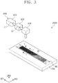
- FIG. 3 is a perspective view of equipment for manufacturing a mask according to an embodiment of the inventive concept.
- a mask manufacturing apparatus 2000 includes a laser irradiation device 600, a stage 700, and a pre-mask MC.
- the mask manufacturing apparatus 2000 is equipment for manufacturing the mask MS (see FIG. 1 ) used in the deposition equipment 1000 (see FIG. 1 ), and may provide the mask MS by removing the front surface of the pre-mask MC. This will be described below in more detail.
- the laser irradiation device 600 includes a laser generation member 610, an optical system 620, and a scanner 630.
- the laser irradiation device 600 may be provided on the stage 700.
- the laser irradiation device 600 is connected to a separate moving unit that may move the laser irradiation device 600 on the stage 700, and may be installed on the stage 700.
- the laser generation member 610 generates a first laser beam L1 that may melt or remove a portion of the pre-mask MC.
- the optical system 620 receives the first laser beam L1, and may control a shape of the first laser beam L1.
- the first laser beam L1 provided from the laser generation member 610 is a laser beam having a Gaussian intensity profile, but a second laser beam L2, which is modified to have a uniform intensity distribution through the optical system 620, is provided. That is, for example, a uniform beam having a flat-top profile may be provided to the scanner 630.
- the optical system 620 may be constituted by a diffractive optical element (DOE) including a beam shaper that serves a beam shaping function.
- DOE diffractive optical element
- Types of light irradiated to the pre-mask MC are not limited thereto, and a Gaussian optical system, a flat-top optical system, a line beam optical system, a multi beam optical system, or the like may be used.
- the scanner 630 adjusts a reflection direction such that the second laser beam L2 provided from the optical system 620 may be irradiated to the mask MC.
- the scanner 630 may be described later in more detail.
- a laser beam L irradiated to the pre-mask MC may be an ultra-short pulsed laser in which a wavelength of transmitted light is extremely short.
- the laser beam L may be a pico-second or a femto-second laser. Accordingly, pattern machining for a very precise unit may be easily performed using the laser beam L.
- the pre-mask MC may be made of a thin plate of an invar material.
- the invar material is an alloy having 64% of iron (Fe) and 36% of nickel (Ni), and it is a material having a very low coefficient of thermal expansion.
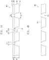
- FIGS. 4A and 4B are cross-sectional views of a mask according to an embodiment of the inventive concept.
- FIG. 4A illustrates a cross-sectional view taken along line I-I' of the pre-mask MC illustrated in FIG. 3 .
- FIG. 4B illustrates a cross-sectional view of a mask MS.
- the mask MS may be provided by the laser machining of the pre-mask MC through the laser irradiation device 600.
- a pre-mask MC1 includes a pattern portion PQ1.
- the pattern portion PQ1 includes a first pattern groove PT1 defined on the front surface of the pre-mask MC1, and a second pattern groove PT2 defined on a rear surface corresponding to the front surface.
- the first pattern groove PT1 and the second pattern groove PT2 may be provided in plurality to the pre-mask MC1.
- the first pattern groove PT1 and the second pattern groove PT2 are disposed to overlap each other, and pass through the pre-mask MC1 to define the pattern portion PQ1.
- the first pattern groove PT1 and the second pattern groove PT2 are illustrated to have inner surfaces of which shapes have curved lines on a cross-section.
- the inner surface of the first pattern groove PT1 has a first curved surface T1
- the inner surface of the second pattern groove PT2 has a second curved surface T2.
- a protrusion R1 is defined at the portion where the first curved surface T1 directly contacts (meets) the second curved surface T2.
- the first pattern groove PT1 and the second pattern groove PT2 have widths that decrease gradually from the front surface and the rear surface, respectively, toward the protrusion R1 of the pre-mask MC1. Also, each of the first curved surface T1 and the second curved surface T2 has a radius of curvature that decreases gradually as it approaches the protrusion R1.
- the first pattern groove PT1 has a first width X1
- the second pattern groove PT2 has a second width X2.
- the first width X1 and the second width X2 may be defined as maximum widths of the first pattern groove PT1 and the second pattern groove PT2, respectively.
- the first width X1 may be measured on the same plane as a first surface S1
- the second width X2 may be measured on the same plane as a second surface S2 corresponding to the first surface S1.
- the first width X1 may be equal to or greater than the second width X2.
- the thickness of the pre-mask MC1 may be defined by the sum of a first thickness W1 corresponding to the depth of the first pattern groove PT1 in the thickness direction from the first surface S1, and a second thickness W2 corresponding to the depth of the second pattern groove PT2 in the thickness direction from the second surface S2.
- the thickness of a first portion M1 may be equal to or greater than the thickness of a second portion M2.
- the pre-mask MC1 may have the thickness ranging from about 10 ⁇ m to about 100 ⁇ m.
- the thickness of the pre-mask MC1 is about 10 ⁇ m or less, it may be difficult to provide an opening that satisfies an intended deposition area.
- a processed depth is from about 1 ⁇ m to about 4 ⁇ m during the machining using the ultra-short pulsed laser, it is desirable for the machining process efficiency that the thickness of the pre-mask MC1 is less than about 100 ⁇ m.
- the first pattern groove PT1 may have the first width X1 ranging form about 15 ⁇ m to about 40 ⁇ m.
- the first width X1 is about 15 ⁇ m or less, a section of the pixel area DA may be narrowly provided, which causes a defect in which the deposition material is not deposited.
- the first width X1 is about 40 ⁇ m or more, a color mixing defect may occur between the adjacent pixels PX.
- the protrusion R1 of the pre-mask MC1 is created during etching processes for the first surface S1 and the second surface S2 of the pre-mask MC1 (see FIGS. 9A to 9D ), and may be provided as the first pattern groove PT1 and the second pattern groove PT2 having different widths that overlap each other in the thickness direction of the pre-mask MC1. That is, the protrusion R1 is produced, as the plurality of pattern grooves overlap each other in the thickness direction.
- the equipment for manufacturing the mask according to an embodiment of the inventive concept aims to remedy the shadow defect.
- the front surface of the pre-mask MC1 is removed through the irradiation of the laser beam L (see FIG. 3 ), and a mask having an opening, in which the protrusion is removed, is provided.
- the cross-sectional view of the mask MS1, which is provided after irradiating the laser beam L to the second surface S2 of the pre-mask MC1 of FIG. 4A is illustrated.
- the laser beam L (see FIG. 3 ) is irradiated to at least one portion of the first portion M1 or the second portion M2 of the pre-mask MC1, and thus at least one portion thereof may be removed.
- the mask MS1 according to an embodiment of the inventive concept, in which the second portion M2 of the pre-mask MC1 is removed, is illustrated.
- the surface, which is removed by the laser beam L has an uneven surface shape QL1.
- the surface, which is not removed by the laser beam L i.e., the surface corresponding to the first surface S1 of the pre-mask MC1 is not damaged by the laser beam L, and this surface may have a relatively even surface shape.
- the protrusion R1 of the pre-mask MC1 is removed by the laser beam L (see FIG. 3 ), and thus the mask MS1 may have an opening P01 corresponding to the first pattern groove PT1.
- the opening PO1 corresponds to the pixel area DA (see FIG. 2 ) of the substrate 300 (see FIG. 1 ), and is an area through which the deposition material is transferred.
- the mask MS1 which is provided by the mask manufacturing apparatus 2000 according to an embodiment of the inventive concept, enables the application of the deposition material to the desired position and with the desired size, by removing the protrusion R1 included in the pre-mask MC1. Therefore, the shadow defect that occurs during the deposition process may be reduced.
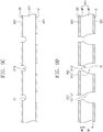
- FIGS. 5A and 5B are cross-sectional views of a mask according to an embodiment of the inventive concept.
- the reference symbols, similar to those of FIGS. 4A and 4B described above, are used, and their duplicated descriptions may not be provided again.
- a pre-mask MC2 includes a pattern portion PQ2.
- the pattern portion PQ2 includes a first pattern groove PT3 defined on a first surface S3 of a pre-mask MC2, and a second pattern groove PT4 defined on a second surface S4 corresponding to the first surface S3.
- the first pattern groove PT3 and the second pattern groove PT4 may be provided in plurality to the pre-mask MC2.
- the first pattern groove PT3 and the second pattern groove PT4 are disposed to overlap each other, and pass through the pre-mask MC2 to define a pattern portion PQ2.
- the inner surface of the first pattern groove PT3 has a first inclined surface T3, and the inner surface of the second pattern groove PT4 has a second inclined surface T4.
- a protrusion R2 is defined at the portion where the first inclined surface T3 directly contacts the second inclined surface T4.
- the first pattern groove PT3 and the second pattern groove PT4 have widths that decrease gradually from the front surface and the rear surface, respectively, toward the protrusion R2 of the pre-mask MC2.
- the first pattern groove PT3 has a first width X3, and the second pattern groove PT4 has a second width X4.
- the first width X3 may be equal to or greater than the second width X4.
- the first pattern groove PT3 and the second pattern groove PT4 according to an embodiment of the inventive concept are illustrated to have inner surfaces of which shapes have inclined lines on a cross-section.
- the thickness of the pre-mask MC2 may be defined by the sum of a first thickness W3 corresponding to the depth of the first pattern groove PT3, and a second thickness W4 corresponding to the depth of the second pattern groove PT4.
- the first thickness W3 may be equal to or greater than the second thickness W4.
- the cross-sectional view of the mask MS2, which is provided after irradiating the laser beam L (see FIG. 3 ) to the second surface S4 of the pre-mask MC2 of FIG. 5A is illustrated.
- the laser beam L is irradiated to at least one portion of the first portion M3 or the second portion M4 of the pre-mask MC2, and thus at least one portion thereof may be removed.
- the mask MS2 according to an embodiment of the inventive concept, in which the second portion M4 of the pre-mask MC2 is removed, is illustrated.
- the surface, which is removed by the laser beam L has an uneven surface shape QL2.
- the surface, which is not removed by the laser beam L, i.e., the surface corresponding to the first surface S3 of the pre-mask MC2 is not damaged by the laser beam L, and this surface may have a relatively even surface shape.
- the protrusion R2 of the pre-mask MC2 is removed by the laser beam L, and thus the mask MS2 may have an opening PO2 corresponding to the first pattern groove PT3.
- the opening PO2 corresponds to the pixel area DA of the substrate 300 (see FIG. 1 ), and is an area through which the deposition material is transferred.
- FIG. 6A is a graph illustrating a probability density distribution of the first laser beam L1 (the laser beam generated in the laser generation member 610), and FIG. 6B is a graph illustrating a probability density distribution of the second laser beam L2 (the laser beam emitted from the optical system 620).
- the first laser beam L1 (see FIG. 3 ), for example, the Gaussian laser beam has an end portion with a convex shape. Therefore, in the case in which the Gaussian laser beam is irradiated to a front surface of the pre-mask MC (see FIG. 3 ) several times while moving in a predetermined direction, the surface to be melted may be uneven. Also, since a direct contact area is small, the processing time required to remove a set or predetermined thickness of the pre-mask MC may increase.
- the second laser beam L2 (see FIG. 3 ), for example, the flat-top beam has an end portion with an even surface shape when compared to the shape of the Gaussian laser beam.
- the first laser beam L1 (the Gaussian shaped laser beam) is transformed into the second laser beam L2 (the flat-top shaped laser beam), and thus may be irradiated to the pre-mask MC.
- the optical system 620 used in the mask manufacturing apparatus 2000 may be constituted by, for example, a diffractive optical element (DOE) including a configuration for the beam shaping function.
- DOE diffractive optical element
- the mask manufacturing apparatus 2000 uses the optical system 620, and thus may be used to transform the Gaussian shaped laser beam produced in the laser generation member 610 into the flat-top shaped laser beam, thereby manufacturing the mask MS (see FIG. 1 ) using the pre-mask MC.
- the flat-top laser beam has the end portion with the flat surface, when it is irradiated to the pre-mask MC, a relatively uniform surface is generated, compared to the shape of Gaussian laser beam, and thus the front surface of the pre-mask MC may be removed. Also, since the area directly contacting the front surface of the pre-mask MC becomes relatively wide, the processing time required to remove a preset or predetermined thickness of the pre-mask MC may be relatively short.
- FIG. 7 is a cross-sectional view of a scanner according to an embodiment of the inventive concept.
- the scanner 630 may be provided with a first mirror 631, a first driving part 632, a second mirror 633, a second driving part 634, and a lens part 635.
- the second laser beam L2 provided through the optical system 620 (see FIG. 3 ) is incident to the scanner 630, and then reflected from the first mirror 631.
- a third laser beam L3 reflected from the first mirror 631 faces toward the second mirror 633.
- the second mirror 633 reflects again the third laser beam L3 reflected from the first mirror 631, and then irradiates the reflected laser beam to the pre-mask MC ( FIG. 3 ).
- the first mirror 631 and the second mirror 633 are driven by the first driving part 632 and the second driving part 634, respectively. That is, the first driving part 632 rotates the first mirror 631, and thus changes the reflection direction of the second laser beam L2 incident to the first mirror 631.
- the second driving part 634 rotates the second mirror 633, and thus changes the reflection direction of the third laser beam L3 reflected from the first mirror 631.
- the first driving part 632 and the second driving part 634 may rotate the first mirror 631 and the second mirror 633, respectively, in different directions.
- the laser beam L may be irradiated onto the pre-mask MC (see FIG. 3 ) while being steered in a first direction DR1 (see FIG. 3 ) and a second direction DR2 (see FIG. 3 ) of the pre-mask MC (e.g., by changing its reflection direction from within the scanner 630) to remove an incident surface portion of the pre-mask MC.
- the lens part 635 functions as collecting the laser beam L reflected from the second mirror 633.
- the lens part 635 may be disposed under the scanner 630 such that the laser beam L is collected and directed toward the pre-mask MC.
- the first mirror 631, the second mirror 633, the first driving part 632, and the second driving part 634 of the scanner 630 may be provided as a galvano scanner. Since provided as the galvano scanner, it is possible to control the direction of the laser beam L, which is provided from the optical system 620 (see FIG. 3 ), by the mirror and the driving parts, which can allow the removal process of the front surface of the pre-mask MC (see FIG. 3 ) to be more precisely performed.
- FIG. 8 is a block diagram illustrating a method for manufacturing a mask according to an embodiment of the inventive concept.
- FIGS. 9A to 9F are views illustrating a process of a method for manufacturing a mask according to an embodiment of the inventive concept.
- the reference symbols, similar to those of FIGS. 3 to 4B , are used, and their duplicated descriptions will be omitted.
- a mask manufacturing method (3000) includes a first etching process (S3100), a second etching process (S3200), and a removing process (S3300).
- the first etching process (S3100) and the second etching process (S3200) are processes that provide a pre-mask
- the removing process (S3300) is a process that removes a portion of the pre-mask to provide a mask.
- the mask manufacturing method will be described in more detail with reference to FIGS. 9A to 9F .
- FIG. 9A to 9D illustrate processes corresponding to the first etching process (S3100) and the second etching process (S3200).
- a first photoresist layer 920 and a second photoresist layer 930 are applied to a first surface S1 and a second surface S2 that corresponds to the first surface S1, respectively, in an initial mask 910.
- the initial mask 910 may be made of a thin plate of an invar material.
- the invar material is an alloy having 64% of Fe and 36% of Ni, and it is a material having a very low coefficient of thermal expansion.
- the first pattern PR1 may have a width U1 that is greater than a width U2 of the second pattern PR2.
- the photolithography process starts with aligning photo-masks that have a plurality of openings with shapes corresponding to patterns that would be defined by the photoresist layers.
- the photo-masks corresponding to photoresist layers, respectively, are aligned. Then, a light exposure process, in which portions of the photoresist layers blocked by the photo-masks are exposed to light, and a developing process, in which the photoresist layers are etched, are performed, and thus the plurality of patterns may be provided.
- the photoresist layers may be provided by applying photoresist solutions on the initial mask 910 through various methods such as a spincoating, a spraying, or a quenching method. In one embodiment, the spincoating method is used, which can uniformly apply the photoresist solution even to a large sized substrate.
- each portion of the first surface S1 and the second surface S2 of the pre-mask 911 exposed by the first pattern PR1 and the second pattern PR2 is wet-etched, and thus a first pattern groove PT1 and a second pattern groove PT2 are provided through the first surface S1 and the second surface S2 of the pre-mask 911, respectively.
- the width of the first pattern groove PT1 is greater than that of the second pattern groove PT2.
- the first pattern groove PT1 and the second pattern groove PT2 are provided to overlap each other, and pass through the pre-mask 911 to define a pattern portion PQ1.
- the inner surface of the first pattern groove PT1 has a first curved surface T1
- the inner surface of the second pattern groove PT2 has a second curved surface T2.
- a protrusion R1 is defined at the portion where the first curved surface T1 directly contacts or meets the second curved surface T2.
- the first pattern groove PT1 and the second pattern groove PT2 have widths that decrease gradually from the first surface S1 and the second surface S2, respectively, toward the protrusion R1 of the pre-mask 911.
- the pre-mask 911 is washed, and then the first photoresist layer 921 and the second photoresist layer 931 may be removed.
- a laser beam L generated in a laser irradiation device 600 is irradiated to a rear surface of the pre-mask 911, in which the second pattern groove PT2 is defined, i.e., the second surface S2 of the pre-mask 911.
- This laser beam L is uniformly irradiated to the rear surface of the pre-mask 911 such that a second portion M2 of the pre-mask 911 is removed.
- a mask MS1 used in the deposition equipment 1000 see FIG. 1 ) is completed.
- the protrusion R1 of the pre-mask 911 is removed by the laser beam L, and thus the mask MS1 may have an opening PO1 corresponding to the first pattern groove PT1.
- the opening PO1 corresponds to the pixel area DA (see FIG. 3 ) of the substrate 300 (see FIG. 1 ), and is an area through which the deposition material is transferred.
- the surface, which is removed by the laser beam L has an uneven surface shape QL1.
- the surface, which is not removed by the laser beam L i.e., the surface corresponding to the first surface S1 of the pre-mask 911 is not damaged by the laser beam L, and this surface may have a relatively even surface shape.
- the mask MS1 in which the protrusion R1 is removed, is provided, and the deposition material is uniformly deposited through the opening PO1 of the mask MS1 during the deposition, which may provide the display device having improved quality.
- the deposition material is uniformly deposited to the display substrate through the opening of the mask during the deposition, which may provide the display device having improved quality.
- the mask manufacturing apparatus and/or any other relevant devices or components according to embodiments of the present invention described herein may be implemented utilizing any suitable hardware, firmware (e.g. an application-specific integrated circuit), software, or a combination of software, firmware, and hardware.
- firmware e.g. an application-specific integrated circuit
- the various components of a controller for the manufacturing apparatus or the laser irradiation device may be formed on one integrated circuit (IC) chip or on separate IC chips.
- the various components of the controller may be implemented on a flexible printed circuit film, a tape carrier package (TCP), a printed circuit board (PCB), or formed on one substrate.
- the various components of the controller may be a process or thread, running on one or more processors, in one or more computing devices, executing computer program instructions and interacting with other system components for performing the various functionalities described herein.
- the computer program instructions are stored in a memory which may be implemented in a computing device using a standard memory device, such as, for example, a random access memory (RAM).
- the computer program instructions may also be stored in other non-transitory computer readable media such as, for example, a CD-ROM, flash drive, or the like.
Landscapes
- Engineering & Computer Science (AREA)
- Optics & Photonics (AREA)
- Physics & Mathematics (AREA)
- Mechanical Engineering (AREA)
- Chemical & Material Sciences (AREA)
- Plasma & Fusion (AREA)
- Manufacturing & Machinery (AREA)
- Chemical Kinetics & Catalysis (AREA)
- Metallurgy (AREA)
- Organic Chemistry (AREA)
- Materials Engineering (AREA)
- General Chemical & Material Sciences (AREA)
- Electroluminescent Light Sources (AREA)
- Physical Vapour Deposition (AREA)
- Laser Beam Processing (AREA)
Abstract
Description
- The present disclosure herein relates to an apparatus for manufacturing a mask and a method for manufacturing a mask.
- Display devices output a video or an image using pixels that have pixel areas, so as to provide various kinds of visual information to a user. Organic light emitting display devices of the display devices have a wide viewing angle, excellent contrast, and fast response speed. The formation of the Pixel areas of these organic light emitting display devices may employ a deposition process to deposit a deposition material. As one example, an organic material is deposited on a substrate through a fine metal mask (FMM) to provide a thin film having a desired pattern.
- As the demand for high resolution display devices increases, an opening of a mask through which the deposition material is transferred also requires a precise manufacturing process. The opening may be made by etching one surface and the other surface of the mask so as to provide a precise opening, but a protrusion is made during the etching process of the both surfaces, which causes the shadow effect that makes it impossible to perform the deposition of the desired shape and size during the deposition process.
- An aspect of the present disclosure relates to an apparatus for manufacturing a mask, so as to provide a mask for solving the above-described limitation.
- An aspect of the present disclosure provides an apparatus for manufacturing a mask, which enables a more precise deposition.
- An embodiment of the inventive concept provides an apparatus for manufacturing a mask, the apparatus including a stage on which a pre-mask is disposed such that a front surface of the pre-mask faces the stage (e.g., faces downward), and a laser irradiation device including a laser generation member configured to irradiate a laser beam to melt or remove a portion of the pre-mask, an optical system configured to receive the laser beam and control a shape of the laser beam, and a scanner configured to adjust a path of the laser beam that has the shape controlled by the optical system, . Here, the pre-mask includes a first portion having a first pattern groove provided through the front surface and a second portion having a second pattern groove provided through a rear surface that faces oppositely away from the front surface, and the first portion and the second portion are arranged in a first direction that is a thickness direction of the pre-mask, and the laser beam with the controlled shape is irradiated onto the second portion of the pre-mask while being steered in a second direction crossing the first direction to remove the second portion to provide a mask having an opening.
- In an embodiment, a width of the first pattern groove is greater than a width of the second pattern groove.
- In an embodiment, the width of the first pattern groove has a maximum width ranging from about 15 µm to about 40 µm.
- In an embodiment, the first pattern groove and the second pattern groove respectively, have widths that decrease gradually from the front surface and the rear surface of the pre-mask in the thickness direction of the pre-mask.
- In an embodiment, a surface of the mask exposed by removing the second portion has an uneven surface shape.
- In an embodiment, the laser beam may be a femto-second laser.
- In an embodiment, the laser beam with the controlled shape may have a flat-top shape.
- In an embodiment, the scanner may include a first mirror configured to reflect the laser beam with the controlled shape, a first driving part configured to rotate the first mirror, a second mirror configured to transmit the laser beam with the controlled shape, which is reflected from the first mirror, to the pre-mask, a second driving part configured to rotate the second mirror, and a lens configured to collect the laser beam with the controlled shape, which is reflected from the second mirror.
- In an embodiment, a shape of an inner surface on a cross-section of each of the first pattern groove and the second pattern groove is formed of either a curved line or a straight line.
- In an embodiment of the inventive concept, an apparatus for manufacturing a mask includes: a stage on which a pre-mask is disposed, the pre-mask having a first surface and a second surface that face oppositely away from each other; and a laser irradiation device including a laser generation member configured to irradiate a laser beam to melt or remove a portion of the pre-mask, an optical system configured to receive the laser beam and control a shape of the laser beam, and a scanner configured to adjust a path of the laser beam that has the shape controlled by the optical system. Here, the pre-mask has a first thickness, the pre-mask includes a pattern portion having a protrusion, the pattern portion being provided in a first direction that is a thickness direction of the pre-mask, and the laser beam with the controlled shape is irradiated on any one of the first surface and the second surface of the pre-mask to provide a mask having a second thickness different from the first thickness and having an opening in which the protrusion is removed.
- In an embodiment, the first thickness may be greater than the second thickness.
- In an embodiment, the width of the opening may have a maximum width ranging from about 15 µm to about 40 µm.
- In an embodiment, a shape of an inner surface of the pattern portion on a cross-section is formed of either a curved line or a straight line.
- In an embodiment, when the shape of the inner surface on a cross section of the pattern portion is the curved line, a radius of curvature may decrease gradually from each of the first surface and the second surface of the mask toward the protrusion.
- In an embodiment, wherein a surface of the mask -- exposed by removing the protrusion -- has an uneven surface shape.
- In an embodiment, the laser beam may be a femto-second laser beam.
- In an embodiment, the laser beam with the controlled shape may have a flat-top shape.
- In an embodiment, the scanner may include a first mirror configured to reflect the laser beam with the controlled shape, a first driving part configured to rotate the first mirror, a second mirror configured to transmit the laser beam with the controlled shape, which is reflected from the first mirror, to the mask, a second driving part configured to rotate the second mirror, and a lens configured to collect the laser beam with the controlled shape, which is reflected from the second mirror.
- In an embodiment of the inventive concept, a method for manufacturing a mask includes performing a first etching in which, for a pre-mask having a first surface and a second surface that face oppositely away from each other, a first pattern groove having a first depth is provided through the first surface, performing a second etching in which a second pattern groove having a second depth is provided through the second surface; and providing a mask that has a front surface having an even surface shape and a rear surface having an uneven surface shape, by removing any one of the first surface and the second surface of the pre-mask, wherein the rear surface is defined by removing any one of the first surface and the second surface.
- In an embodiment, the providing of the mask may include irradiating a laser beam onto the front surface of the pre-mask and removing any one of the first surface and the second surface of the pre-mask.
- At least some of the above features that accord with the invention, and other features according to the invention, are set-out in the claims.
- The drawings illustrate embodiments of the inventive concept and, together with the description, serve to explain principles of the inventive concept. In the drawings:
-
FIG. 1 is a schematic view of deposition equipment using a mask according to an embodiment of the inventive concept; -
FIG. 2 is a cross-sectional view illustrating a portion of a pixel area in a substrate according to an embodiment of the inventive concept; -
FIG. 3 is a perspective view of equipment for manufacturing a mask according to an embodiment of the inventive concept; -
FIGS. 4A and 4B are cross-sectional views of a mask according to an embodiment of the inventive concept; -
FIGS. 5A and 5B are cross-sectional views of a mask according to an embodiment of the inventive concept; -
FIGS. 6A and 6B illustrate shapes of laser according to an embodiment of the inventive concept; -
FIG. 7 is a cross-sectional view of a scanner according to an embodiment of the inventive concept; -
FIG. 8 is a block diagram illustrating a method for manufacturing a mask according to an embodiment of the inventive concept; and -
FIGS. 9A to 9F are views illustrating a process of a method for manufacturing a mask according to an embodiment of the inventive concept. - Since an embodiment of the inventive concept may have various modifications and diverse shapes, particular embodiments are illustrated in the drawings and are described in the detailed description. However, the scope of the present invention is not limited to the disclosure of these particular embodiments.
- When explaining each of the drawings, like reference numerals are used for referring to like elements. In the accompanying drawings, the dimensions of structures are scaled up or down from the real ones for clarity of the present disclosure. It will be understood that although the terms of first and second are used herein to describe various elements, these elements should not be limited by these terms. Terms are only used to distinguish one component from other components. For example, a first element can be referred to as a second element, and similarly a second element can be referred to as a first element without departing from the scope of the present disclosure. The terms of a singular form may include plural forms unless definitely indicating a particular case in terms of the context.
- In the application, it will be understood that the meaning of "include" or "comprise" specifies the presence of a property, a fixed number, a step, a process, an element, a component, or a combination thereof disclosed in the specification but does not exclude the possibility of the presence or addition of one or more of properties, fixed numbers, steps, processes, elements, components, or combinations thereof in advance.
- For an embodiment of the inventive concept so as to achieve the above-described purpose, certain embodiments of the inventive concept will be described in more detail with reference to the accompanying drawings hereinafter.
- Spatially relative terms, such as "beneath", "below", "lower", "under", "above", "upper" and the like, may be used herein for ease of description to describe one element or feature's relationship to another element(s) or feature(s) as illustrated in the figures. It will be understood that the spatially relative terms are intended to encompass different orientations of the device in use or in operation, in addition to the orientation depicted in the figures. For example, if the device in the figures is turned over, elements described as "below" or "beneath" or "under" other elements or features would then be oriented "above" the other elements or features. Thus, the example terms "below" and "under" can encompass both an orientation of above and below. The device may be otherwise oriented (e.g., rotated 90 degrees or at other orientations) and the spatially relative descriptors used herein should be interpreted accordingly. In addition, it will also be understood that when a layer is referred to as being "between" two layers, it can be the only layer between the two layers, or one or more intervening layers may also be present.
- The use of "may" when describing embodiments of the inventive concept refers to "one or more embodiments of the inventive concept."
- It will be understood that when an element or layer is referred to as being "on", "connected to", "coupled to", or "adjacent to" another element or layer, it can be directly on, connected to, coupled to, or adjacent to the other element or layer, or one or more intervening elements or layers may be present. In contrast, when an element or layer is referred to as being "directly on," "directly connected to", "directly coupled to", or "immediately adjacent to" another element or layer, there are no intervening elements or layers present.
- As used herein, the term "substantially," "about," and similar terms are used as terms of approximation and not as terms of degree, and are intended to account for the inherent deviations in measured or calculated values that would be recognized by those of ordinary skill in the art. Also, any numerical range recited herein is intended to include all sub-ranges of the same numerical precision subsumed within the recited range. For example, a range of "1.0 to 10.0" is intended to include all subranges between (and including) the recited minimum value of 1.0 and the recited maximum value of 10.0, that is, having a minimum value equal to or greater than 1.0 and a maximum value equal to or less than 10.0, such as, for example, 2.4 to 7.6. Any maximum numerical limitation recited herein is intended to include all lower numerical limitations subsumed therein and any minimum numerical limitation recited in this specification is intended to include all higher numerical limitations subsumed therein. Accordingly, Applicant reserves the right to amend this specification, including the claims, to expressly recite any sub-range subsumed within the ranges expressly recited herein.
- As used herein, the terms "use," "using," and "used" may be considered synonymous with the terms "utilize," "utilizing," and "utilized," respectively.
-
FIG. 1 is a schematic view of deposition equipment using a mask according to an embodiment of the inventive concept.FIG. 2 is a cross-sectional view illustrating a portion of a pixel area in a substrate according to an embodiment of the inventive concept. Referring toFIGS. 1 and2 , a mask and a display substrate provided by the mask will be described in more detail. -
Deposition equipment 1000 includes achamber 100, asubstrate seat 200, asubstrate 300, amask frame 400, adeposition source 500, and a mask MS. Thedeposition equipment 1000 is used to provide a plurality of thin film patterns, which are included in a display device, on thesubstrate 300. - Inside the
chamber 100, a space may be defined therein. Thesubstrate seat 200, thesubstrate 300, themask frame 400, thedeposition source 500, and the mask MS may be disposed within the inner space. In the mask MS, an opening PO may be provided, and the opening PO corresponds to an area through which a deposition material DM is transferred. - The
substrate 300 is disposed on (e.g., under) thesubstrate seat 200, and thesubstrate seat 200 supports thesubstrate 300. Thesubstrate seat 200 may be provided in various forms as long as it has a general structure capable of supporting thesubstrate 300. For example, thesubstrate seat 300 may include a shuttle, an electrostatic chuck, or the like, which is disposed within thechamber 100. - The deposition material DM is deposited on the
substrate 300 through the opening PO of the mask MS, and an area deposited with the deposition material DM may be defined as a pixel area DA that emits light. A non-pixel area NDA may be defined between adjacent pixel areas. - The
mask frame 400 may be made of metal with high strength. Accordingly, the deformation of themask frame 400, which may occur during welding, may be reduced, and thus a process may be stably performed, and a lifespan of themask frame 400 may be increased. - In one embodiment, a welded portion, in which the
mask frame 400 and the mask MS are welded and coupled, may be formed. A high temperature is generated around this welded portion, and thus themask frame 400 may be made of a material having the low thermal deformation. - The
deposition source 500 provides the deposition material DM to the substrate. Thedeposition source 500 may be provided with a set or predetermined inner space so as to accommodate the deposition material DM. - Here, the deposition material may be a material to be sublimated or vaporized, and include at least one of an inorganic substance, metal, or an organic substance. For example, a suctioning or vacuum part is operated after the
chamber 100 is closed, and thus may maintain the pressure inside thechamber 100 in a substantially vacuum state. Also, thedeposition source 500 may make the deposition material DM vaporized or sublimated, and accordingly, the deposition material DM passes through the mask MS and may be deposited on thesubstrate 300. Here, the deposition material passes through the opening PO in the mask MS, and thus may be deposited, on the substrate, in a regular pattern. - The deposition material DM is transferred through the mask MS and deposited on the
substrate 300, and thus a deposition pattern EML is defined. The shape of the deposition pattern EML may correspond to the opening PO. The deposition pattern EML may be a light emitting pattern EML, which will be described later. Here, the deposition material DM may include a light emitting material. However, this is merely described as an example. Depending on the deposition material DM provided by thedeposition source 500, the deposition pattern EML may be various suitable patterns that constitute a display panel DP that will be described later, and is not limited to one embodiment. - As illustrated in
FIG. 2 , the display panel DP includes a display layer DPL, a thin film encapsulation layer TFE, a color filter layer CFL, and a protection layer PTL. - The display layer DPL includes a base layer SUB, a pixel PX, and a plurality of insulation layers IL1, IL2, and IL3. The pixel PX includes a thin film transistor TFT and an organic light emitting element OLED.
- The first insulation layer IL1 and a semiconductor pattern AL of the thin film transistor TFT are disposed on the base layer SUB. The first insulation layer IL1 covers the semiconductor pattern AL.
- The second insulation layer IL2 and a control (e.g., gate) electrode GE of the thin film transistor TFT are disposed on the first insulation layer IL1. The second insulation layer IL2 covers the control electrode GE. Each of the first insulation layer IL1 and the second insulation layer IL2 includes an organic film and/or an inorganic film. Each of the first insulation layer IL1 and the second insulation layer IL2 may include a plurality of thin films.
- The third insulation layer IL3, and input and output (e.g., source and drain) electrodes SE and DE of the thin film transistor TFT are disposed on the second insulation layer IL2. The third insulation layer IL3 covers the input and output electrodes SE and DE.
- The input and output electrodes SE and DE are connected to the semiconductor pattern AL through first and second through-holes CH1 and CH2, which penetrate the first and second insulation layers IL1 and IL2, respectively. Here, this is merely illustrated as an example. A layer, in which the control electrode GE, the input electrode SE, the output electrode DE, and the semiconductor pattern AL are disposed, may be diversely or suitably changed. The control electrode GE, the input electrode SE, and the output electrode DE may directly contact the semiconductor AL without a separate through-hole. Thin film transistor TFT according to an embodiment of the inventive concept may be provided in various structures, and is not limited to any one embodiment.
- The organic light emitting element OLED and a pixel defining film PDL are disposed on the third insulation layer IL3. The organic light emitting element OLED includes an anode electrode AE, a light emitting pattern EML, a cathode electrode CE, a hole transport region CL1 defined between the anode electrode AE and the light emitting pattern EML, and an electron transport region CL2 defined between the light emitting pattern EML and the cathode electrode CE. The anode electrode AE is provided in plurality, and each may be disposed to overlap a corresponding one of the pixel areas (along a thickness direction of the display panel DP).
- The pixel defining film PDL is disposed on the anode electrode AE, and exposes a portion of the anode electrode AE. The pixel defining film PDL substantially defines the pixel area DA. Here, the anode electrode AE is connected to the output electrode DE through a third through-hole CH3 defined in the third insulation layer IL3.
- The hole transport region CL1 is disposed on the anode electrode AE, and covers the anode electrode AE and the pixel defining film PDL. The hole transport region CL1 may include at least any one of a hole injection layer, a hole transport layer, or a single layer having both a hole injecting function and a hole transporting function.
- The light emitting pattern EML is disposed on the hole transport region CL1. The light emitting pattern EML is provided in plurality, and each overlaps a corresponding one of light emitting areas (along a thickness direction of the display panel DP). The light emitting pattern EML may include a phosphorescent material and a fluorescent material. The light emitting pattern EML may generate light having one color, or light in which two or more colors are mixed.
- According to an embodiment of the inventive concept, the
substrate 300 provided to thedeposition equipment 1000 may be supplied in a state in which layers up to the hole transport region CL1, which is a portion of the display layer DPL, are laminated. However, this is an example, and a lamination configuration of thesubstrate 300 provided to thedeposition equipment 1000 is not limited to any one example. - The electron transport region CL2 is disposed on the light emitting pattern EML, and covers the light emitting pattern EML and the hole transport region CL1. The electron transport region CL2 may include at least any one of an electron transport material or an electron injection material. For example, the electron transport region CL2 may be an electron transport layer having the electron transport material, or an electron injection/transport single layer having the electron transport material and the electron injection material.
- The cathode electrode CE is disposed on the electron transport region CL2, and faces the anode electrode AE. The cathode electrode CE may be made of a material having a low work function so as to enable easy electron injection.
- The cathode electrode CE and the anode AE may be made of different materials, depending on a light emitting method. For example, when the pixel area DA according to the inventive concept is a front-light emitting type, the cathode electrode CE may be a transmissive electrode, and the anode electrode AE may be a reflective electrode.
- Alternatively, for example, when the pixel area DA according to the inventive concept is a rear-light emitting type, the cathode electrode CE may be a reflective electrode, and the anode electrode AE may be a transmissive electrode. Here, positions of the cathode electrode CE and the anode electrode AE are not limited thereto, and may be suitably changed.
- The pixel area DA according to the inventive concept may include organic light emitting elements having various suitable structures, and are not limited to any one embodiment.
- The thin film encapsulation layer TFE is disposed on the cathode electrode CE. The thin film encapsulation layer TFE covers an entire surface of the cathode electrode CE, and encapsulates the organic light emitting element OLED. The thin film encapsulation layer TFE may have a thickness ranging from about 1 µm to about 10 µm. The pixel area DA includes the thin film encapsulation layer TFE, and thus a thin-film type pixel area DA may be realized.
- The thin film encapsulation layer TFE may include a plurality of inorganic films and/or organic films. The inorganic films and the organic films may be alternately disposed. The inorganic film protects the organic light emitting element OLED against moisture/oxygen, and the organic film protects the organic light emitting element OLED against impurities such as dust particles. The inorganic film may include a nitride layer, a silicon oxynitride layer, a silicon oxide layer, a titanium oxide layer, an aluminum oxide layer, or the like. The organic film may include an acrylic-based organic film, but is not particularly limited thereto.
- The color filter layer CFL includes a black matrix BM and color patterns CP. The black matrix BM and the color patterns CP are disposed on the same layer. The black matrix BM and the color patterns CP are directly disposed on the thin film encapsulation layer TFE, and contact a top surface of the thin film encapsulation layer TFE.
- The black matrix BM may be made of a light blocking material. The black matrix BM absorbs light incident to the black matrix BM. Accordingly, the black matrix BM may have mainly a black-based color. The color patterns CP include color patterns having at least two different colors. The color patterns CP may have four or more colors, and portions of the adjacent color patterns may have the same color. The color filter layer CFL according to the inventive concept may include various embodiments, and is not limited to any one embodiment. Also, the color filter layer CFL may be omitted.
- The protection layer PTL is disposed on the color filter layer CFL, and protects the color filter layer CFL. The protection layer PTL provides a flat surface in an upper portion. The flat surface corresponds to the front surface of the pixel area DA. However, this is merely illustrated as an example. The protection layer PTL may be omitted in the pixel area DA according to an embodiment of the inventive concept.
- The mask MS illustrated in
FIG. 1 may be applied to a process for manufacturing various suitable elements that constitute the pixel area DA. For example, thesubstrate 300 illustrated inFIG. 1 may be provided in a state in which the hole transport region CL1 is laminated to each region corresponding to the opening PO of the mask. - Then, the light emitting pattern EML is provided through the mask MS. Accordingly, the mask MS may be applied in a process of defining the light emitting pattern EML. However, this is merely disclosed as an example. The mask MS according to an embodiment of the inventive concept may be applied to various suitable processes, and is not limited thereto.
-
FIG. 3 is a perspective view of equipment for manufacturing a mask according to an embodiment of the inventive concept. - Referring to
FIG. 3 , amask manufacturing apparatus 2000 includes alaser irradiation device 600, astage 700, and a pre-mask MC. Themask manufacturing apparatus 2000 is equipment for manufacturing the mask MS (seeFIG. 1 ) used in the deposition equipment 1000 (seeFIG. 1 ), and may provide the mask MS by removing the front surface of the pre-mask MC. This will be described below in more detail. - The
laser irradiation device 600 includes alaser generation member 610, anoptical system 620, and ascanner 630. Thelaser irradiation device 600 may be provided on thestage 700. In one embodiment, thelaser irradiation device 600 is connected to a separate moving unit that may move thelaser irradiation device 600 on thestage 700, and may be installed on thestage 700. - The
laser generation member 610 generates a first laser beam L1 that may melt or remove a portion of the pre-mask MC. Theoptical system 620 receives the first laser beam L1, and may control a shape of the first laser beam L1. For example, the first laser beam L1 provided from thelaser generation member 610 is a laser beam having a Gaussian intensity profile, but a second laser beam L2, which is modified to have a uniform intensity distribution through theoptical system 620, is provided. That is, for example, a uniform beam having a flat-top profile may be provided to thescanner 630. Theoptical system 620 may be constituted by a diffractive optical element (DOE) including a beam shaper that serves a beam shaping function. - Types of light irradiated to the pre-mask MC are not limited thereto, and a Gaussian optical system, a flat-top optical system, a line beam optical system, a multi beam optical system, or the like may be used.
- The
scanner 630 adjusts a reflection direction such that the second laser beam L2 provided from theoptical system 620 may be irradiated to the mask MC. Thescanner 630 may be described later in more detail. - According to an embodiment of the inventive concept, a laser beam L irradiated to the pre-mask MC may be an ultra-short pulsed laser in which a wavelength of transmitted light is extremely short. For example, the laser beam L may be a pico-second or a femto-second laser. Accordingly, pattern machining for a very precise unit may be easily performed using the laser beam L.
- The pre-mask MC may be made of a thin plate of an invar material. For example, the invar material is an alloy having 64% of iron (Fe) and 36% of nickel (Ni), and it is a material having a very low coefficient of thermal expansion.
-
FIGS. 4A and 4B are cross-sectional views of a mask according to an embodiment of the inventive concept.FIG. 4A illustrates a cross-sectional view taken along line I-I' of the pre-mask MC illustrated inFIG. 3 .FIG. 4B illustrates a cross-sectional view of a mask MS. The mask MS may be provided by the laser machining of the pre-mask MC through thelaser irradiation device 600. - A pre-mask MC1 includes a pattern portion PQ1. The pattern portion PQ1 includes a first pattern groove PT1 defined on the front surface of the pre-mask MC1, and a second pattern groove PT2 defined on a rear surface corresponding to the front surface. The first pattern groove PT1 and the second pattern groove PT2 may be provided in plurality to the pre-mask MC1. The first pattern groove PT1 and the second pattern groove PT2 are disposed to overlap each other, and pass through the pre-mask MC1 to define the pattern portion PQ1.
- The first pattern groove PT1 and the second pattern groove PT2 according to an embodiment of the inventive concept are illustrated to have inner surfaces of which shapes have curved lines on a cross-section. The inner surface of the first pattern groove PT1 has a first curved surface T1, and the inner surface of the second pattern groove PT2 has a second curved surface T2. A protrusion R1 is defined at the portion where the first curved surface T1 directly contacts (meets) the second curved surface T2.
- The first pattern groove PT1 and the second pattern groove PT2 have widths that decrease gradually from the front surface and the rear surface, respectively, toward the protrusion R1 of the pre-mask MC1. Also, each of the first curved surface T1 and the second curved surface T2 has a radius of curvature that decreases gradually as it approaches the protrusion R1.
- The first pattern groove PT1 has a first width X1, and the second pattern groove PT2 has a second width X2. The first width X1 and the second width X2 may be defined as maximum widths of the first pattern groove PT1 and the second pattern groove PT2, respectively. The first width X1 may be measured on the same plane as a first surface S1, and the second width X2 may be measured on the same plane as a second surface S2 corresponding to the first surface S1. The first width X1 may be equal to or greater than the second width X2.
- The thickness of the pre-mask MC1 may be defined by the sum of a first thickness W1 corresponding to the depth of the first pattern groove PT1 in the thickness direction from the first surface S1, and a second thickness W2 corresponding to the depth of the second pattern groove PT2 in the thickness direction from the second surface S2. The thickness of a first portion M1 may be equal to or greater than the thickness of a second portion M2.
- The pre-mask MC1 according to an embodiment of the inventive concept may have the thickness ranging from about 10 µm to about 100 µm. When the thickness of the pre-mask MC1 is about 10 µm or less, it may be difficult to provide an opening that satisfies an intended deposition area. Also, since a processed depth is from about 1 µm to about 4 µm during the machining using the ultra-short pulsed laser, it is desirable for the machining process efficiency that the thickness of the pre-mask MC1 is less than about 100 µm.
- The first pattern groove PT1 may have the first width X1 ranging form about 15 µm to about 40 µm. When the first width X1 is about 15 µm or less, a section of the pixel area DA may be narrowly provided, which causes a defect in which the deposition material is not deposited. When the first width X1 is about 40 µm or more, a color mixing defect may occur between the adjacent pixels PX.
- The protrusion R1 of the pre-mask MC1 is created during etching processes for the first surface S1 and the second surface S2 of the pre-mask MC1 (see
FIGS. 9A to 9D ), and may be provided as the first pattern groove PT1 and the second pattern groove PT2 having different widths that overlap each other in the thickness direction of the pre-mask MC1. That is, the protrusion R1 is produced, as the plurality of pattern grooves overlap each other in the thickness direction. - There may be a shadow defect in which, during the deposition process, a deposition area is expanded due to the protrusion R1 and thus a deposition area for emitting another light is breached. As a result, when a mask having the above-described pre-mask MC1 is used in the deposition process, the quality degradation of the display device, such as the manufacture of defective products, may be caused.
- The equipment for manufacturing the mask according to an embodiment of the inventive concept aims to remedy the shadow defect. The front surface of the pre-mask MC1 is removed through the irradiation of the laser beam L (see
FIG. 3 ), and a mask having an opening, in which the protrusion is removed, is provided. - As illustrated in
FIG. 4B , the cross-sectional view of the mask MS1, which is provided after irradiating the laser beam L to the second surface S2 of the pre-mask MC1 ofFIG. 4A , is illustrated. For example, the laser beam L (seeFIG. 3 ) is irradiated to at least one portion of the first portion M1 or the second portion M2 of the pre-mask MC1, and thus at least one portion thereof may be removed. In the cross-sectional view, the mask MS1 according to an embodiment of the inventive concept, in which the second portion M2 of the pre-mask MC1 is removed, is illustrated. - The surface, which is removed by the laser beam L, has an uneven surface shape QL1. The surface, which is not removed by the laser beam L, i.e., the surface corresponding to the first surface S1 of the pre-mask MC1 is not damaged by the laser beam L, and this surface may have a relatively even surface shape.
- The protrusion R1 of the pre-mask MC1 is removed by the laser beam L (see
FIG. 3 ), and thus the mask MS1 may have an opening P01 corresponding to the first pattern groove PT1. The opening PO1 corresponds to the pixel area DA (seeFIG. 2 ) of the substrate 300 (seeFIG. 1 ), and is an area through which the deposition material is transferred. - The mask MS1, which is provided by the
mask manufacturing apparatus 2000 according to an embodiment of the inventive concept, enables the application of the deposition material to the desired position and with the desired size, by removing the protrusion R1 included in the pre-mask MC1. Therefore, the shadow defect that occurs during the deposition process may be reduced. -
FIGS. 5A and 5B are cross-sectional views of a mask according to an embodiment of the inventive concept. The reference symbols, similar to those ofFIGS. 4A and 4B described above, are used, and their duplicated descriptions may not be provided again. - A pre-mask MC2 includes a pattern portion PQ2. The pattern portion PQ2 includes a first pattern groove PT3 defined on a first surface S3 of a pre-mask MC2, and a second pattern groove PT4 defined on a second surface S4 corresponding to the first surface S3. The first pattern groove PT3 and the second pattern groove PT4 may be provided in plurality to the pre-mask MC2. The first pattern groove PT3 and the second pattern groove PT4 are disposed to overlap each other, and pass through the pre-mask MC2 to define a pattern portion PQ2. The inner surface of the first pattern groove PT3 has a first inclined surface T3, and the inner surface of the second pattern groove PT4 has a second inclined surface T4. A protrusion R2 is defined at the portion where the first inclined surface T3 directly contacts the second inclined surface T4.
- The first pattern groove PT3 and the second pattern groove PT4 have widths that decrease gradually from the front surface and the rear surface, respectively, toward the protrusion R2 of the pre-mask MC2.
- The first pattern groove PT3 has a first width X3, and the second pattern groove PT4 has a second width X4. The first width X3 may be equal to or greater than the second width X4. The first pattern groove PT3 and the second pattern groove PT4 according to an embodiment of the inventive concept are illustrated to have inner surfaces of which shapes have inclined lines on a cross-section.
- The thickness of the pre-mask MC2 may be defined by the sum of a first thickness W3 corresponding to the depth of the first pattern groove PT3, and a second thickness W4 corresponding to the depth of the second pattern groove PT4. The first thickness W3 may be equal to or greater than the second thickness W4.
- As illustrated in
FIG. 5B , the cross-sectional view of the mask MS2, which is provided after irradiating the laser beam L (seeFIG. 3 ) to the second surface S4 of the pre-mask MC2 ofFIG. 5A , is illustrated. For example, the laser beam L is irradiated to at least one portion of the first portion M3 or the second portion M4 of the pre-mask MC2, and thus at least one portion thereof may be removed. In the cross-sectional view, the mask MS2 according to an embodiment of the inventive concept, in which the second portion M4 of the pre-mask MC2 is removed, is illustrated. In the mask MS2, the surface, which is removed by the laser beam L, has an uneven surface shape QL2. - The surface, which is not removed by the laser beam L, i.e., the surface corresponding to the first surface S3 of the pre-mask MC2 is not damaged by the laser beam L, and this surface may have a relatively even surface shape.
- The protrusion R2 of the pre-mask MC2 is removed by the laser beam L, and thus the mask MS2 may have an opening PO2 corresponding to the first pattern groove PT3. The opening PO2 corresponds to the pixel area DA of the substrate 300 (see
FIG. 1 ), and is an area through which the deposition material is transferred. -
FIG. 6A is a graph illustrating a probability density distribution of the first laser beam L1 (the laser beam generated in the laser generation member 610), andFIG. 6B is a graph illustrating a probability density distribution of the second laser beam L2 (the laser beam emitted from the optical system 620). - Referring to
FIG. 6A , the first laser beam L1 (seeFIG. 3 ), for example, the Gaussian laser beam has an end portion with a convex shape. Therefore, in the case in which the Gaussian laser beam is irradiated to a front surface of the pre-mask MC (seeFIG. 3 ) several times while moving in a predetermined direction, the surface to be melted may be uneven. Also, since a direct contact area is small, the processing time required to remove a set or predetermined thickness of the pre-mask MC may increase. - Referring to
FIG. 6B , the second laser beam L2 (seeFIG. 3 ), for example, the flat-top beam has an end portion with an even surface shape when compared to the shape of the Gaussian laser beam. Through the optical system 630 (seeFIG. 3 ), the first laser beam L1 (the Gaussian shaped laser beam) is transformed into the second laser beam L2 (the flat-top shaped laser beam), and thus may be irradiated to the pre-mask MC. - The
optical system 620 used in the mask manufacturing apparatus 2000 (seeFIG. 3 ) may be constituted by, for example, a diffractive optical element (DOE) including a configuration for the beam shaping function. Themask manufacturing apparatus 2000 according to the inventive concept uses theoptical system 620, and thus may be used to transform the Gaussian shaped laser beam produced in thelaser generation member 610 into the flat-top shaped laser beam, thereby manufacturing the mask MS (seeFIG. 1 ) using the pre-mask MC. - Since the flat-top laser beam has the end portion with the flat surface, when it is irradiated to the pre-mask MC, a relatively uniform surface is generated, compared to the shape of Gaussian laser beam, and thus the front surface of the pre-mask MC may be removed. Also, since the area directly contacting the front surface of the pre-mask MC becomes relatively wide, the processing time required to remove a preset or predetermined thickness of the pre-mask MC may be relatively short.
-
FIG. 7 is a cross-sectional view of a scanner according to an embodiment of the inventive concept. - As illustrated in
FIG. 7 , thescanner 630 may be provided with afirst mirror 631, afirst driving part 632, asecond mirror 633, asecond driving part 634, and alens part 635. - The second laser beam L2 provided through the optical system 620 (see
FIG. 3 ) is incident to thescanner 630, and then reflected from thefirst mirror 631. A third laser beam L3 reflected from thefirst mirror 631 faces toward thesecond mirror 633. Thesecond mirror 633 reflects again the third laser beam L3 reflected from thefirst mirror 631, and then irradiates the reflected laser beam to the pre-mask MC (FIG. 3 ). Thefirst mirror 631 and thesecond mirror 633 are driven by thefirst driving part 632 and thesecond driving part 634, respectively. That is, thefirst driving part 632 rotates thefirst mirror 631, and thus changes the reflection direction of the second laser beam L2 incident to thefirst mirror 631. Also, thesecond driving part 634 rotates thesecond mirror 633, and thus changes the reflection direction of the third laser beam L3 reflected from thefirst mirror 631. Thefirst driving part 632 and thesecond driving part 634 may rotate thefirst mirror 631 and thesecond mirror 633, respectively, in different directions. The laser beam L may be irradiated onto the pre-mask MC (seeFIG. 3 ) while being steered in a first direction DR1 (seeFIG. 3 ) and a second direction DR2 (seeFIG. 3 ) of the pre-mask MC (e.g., by changing its reflection direction from within the scanner 630) to remove an incident surface portion of the pre-mask MC. - The
lens part 635 functions as collecting the laser beam L reflected from thesecond mirror 633. Thelens part 635 may be disposed under thescanner 630 such that the laser beam L is collected and directed toward the pre-mask MC. - The
first mirror 631, thesecond mirror 633, thefirst driving part 632, and thesecond driving part 634 of thescanner 630 according to an embodiment of the inventive concept may be provided as a galvano scanner. Since provided as the galvano scanner, it is possible to control the direction of the laser beam L, which is provided from the optical system 620 (seeFIG. 3 ), by the mirror and the driving parts, which can allow the removal process of the front surface of the pre-mask MC (seeFIG. 3 ) to be more precisely performed. -
FIG. 8 is a block diagram illustrating a method for manufacturing a mask according to an embodiment of the inventive concept.FIGS. 9A to 9F are views illustrating a process of a method for manufacturing a mask according to an embodiment of the inventive concept. The reference symbols, similar to those ofFIGS. 3 to 4B , are used, and their duplicated descriptions will be omitted. - As illustrated in
FIG. 8 , a mask manufacturing method (3000) includes a first etching process (S3100), a second etching process (S3200), and a removing process (S3300). The first etching process (S3100) and the second etching process (S3200) are processes that provide a pre-mask, and the removing process (S3300) is a process that removes a portion of the pre-mask to provide a mask. Hereinafter, the mask manufacturing method will be described in more detail with reference toFIGS. 9A to 9F . -
FIG. 9A to 9D illustrate processes corresponding to the first etching process (S3100) and the second etching process (S3200). As illustrated inFIG. 9A , afirst photoresist layer 920 and asecond photoresist layer 930 are applied to a first surface S1 and a second surface S2 that corresponds to the first surface S1, respectively, in aninitial mask 910. As one example, theinitial mask 910 may be made of a thin plate of an invar material. Here, the invar material is an alloy having 64% of Fe and 36% of Ni, and it is a material having a very low coefficient of thermal expansion. - Then, as illustrated in
FIG, 9B , a photolithography process is performed on theinitial mask 910, and thus a first pattern PR1 and a second pattern PR2 is provided in afirst photoresist layer 921 and asecond photoresist layer 931, respectively. The first pattern PR1 may have a width U1 that is greater than a width U2 of the second pattern PR2. - First, the photolithography process starts with aligning photo-masks that have a plurality of openings with shapes corresponding to patterns that would be defined by the photoresist layers.
- The photo-masks corresponding to photoresist layers, respectively, are aligned. Then, a light exposure process, in which portions of the photoresist layers blocked by the photo-masks are exposed to light, and a developing process, in which the photoresist layers are etched, are performed, and thus the plurality of patterns may be provided. The photoresist layers may be provided by applying photoresist solutions on the
initial mask 910 through various methods such as a spincoating, a spraying, or a quenching method. In one embodiment, the spincoating method is used, which can uniformly apply the photoresist solution even to a large sized substrate. - Then, as illustrated in
FIGS. 9C and 9D , each portion of the first surface S1 and the second surface S2 of the pre-mask 911 exposed by the first pattern PR1 and the second pattern PR2 is wet-etched, and thus a first pattern groove PT1 and a second pattern groove PT2 are provided through the first surface S1 and the second surface S2 of the pre-mask 911, respectively. Here, the width of the first pattern groove PT1 is greater than that of the second pattern groove PT2. The first pattern groove PT1 and the second pattern groove PT2 are provided to overlap each other, and pass through the pre-mask 911 to define a pattern portion PQ1. Through the wetetching process, the inner surface of the first pattern groove PT1 has a first curved surface T1, and the inner surface of the second pattern groove PT2 has a second curved surface T2. A protrusion R1 is defined at the portion where the first curved surface T1 directly contacts or meets the second curved surface T2. - The first pattern groove PT1 and the second pattern groove PT2 have widths that decrease gradually from the first surface S1 and the second surface S2, respectively, toward the protrusion R1 of the pre-mask 911.
- After the first pattern groove PT1 and the second pattern groove PT2 are defined, the pre-mask 911 is washed, and then the
first photoresist layer 921 and thesecond photoresist layer 931 may be removed. - As illustrated in
FIGS. 9E and9F , a laser beam L generated in alaser irradiation device 600 is irradiated to a rear surface of the pre-mask 911, in which the second pattern groove PT2 is defined, i.e., the second surface S2 of the pre-mask 911. This laser beam L is uniformly irradiated to the rear surface of the pre-mask 911 such that a second portion M2 of the pre-mask 911 is removed. After the second portion M2 is all removed, a mask MS1 used in the deposition equipment 1000 (seeFIG. 1 ) is completed. - The protrusion R1 of the pre-mask 911 is removed by the laser beam L, and thus the mask MS1 may have an opening PO1 corresponding to the first pattern groove PT1. The opening PO1 corresponds to the pixel area DA (see
FIG. 3 ) of the substrate 300 (seeFIG. 1 ), and is an area through which the deposition material is transferred. - The surface, which is removed by the laser beam L, has an uneven surface shape QL1. The surface, which is not removed by the laser beam L, i.e., the surface corresponding to the first surface S1 of the pre-mask 911 is not damaged by the laser beam L, and this surface may have a relatively even surface shape.
- In the mask manufacturing method according to an embodiment of the inventive concept, the mask MS1, in which the protrusion R1 is removed, is provided, and the deposition material is uniformly deposited through the opening PO1 of the mask MS1 during the deposition, which may provide the display device having improved quality.
- According to an embodiment of the inventive concept, the deposition material is uniformly deposited to the display substrate through the opening of the mask during the deposition, which may provide the display device having improved quality.
- The mask manufacturing apparatus and/or any other relevant devices or components according to embodiments of the present invention described herein may be implemented utilizing any suitable hardware, firmware (e.g. an application-specific integrated circuit), software, or a combination of software, firmware, and hardware. For example, the various components of a controller for the manufacturing apparatus or the laser irradiation device may be formed on one integrated circuit (IC) chip or on separate IC chips. Further, the various components of the controller may be implemented on a flexible printed circuit film, a tape carrier package (TCP), a printed circuit board (PCB), or formed on one substrate. Further, the various components of the controller may be a process or thread, running on one or more processors, in one or more computing devices, executing computer program instructions and interacting with other system components for performing the various functionalities described herein. The computer program instructions are stored in a memory which may be implemented in a computing device using a standard memory device, such as, for example, a random access memory (RAM). The computer program instructions may also be stored in other non-transitory computer readable media such as, for example, a CD-ROM, flash drive, or the like. Also, a person of skill in the art should recognize that the functionality of various computing devices may be combined or integrated into a single computing device, or the functionality of a particular computing device may be distributed across one or more other computing devices without departing from the scope of the exemplary embodiments of the present invention.
- While specific terms were used herein, they were not used to limit the meaning or the scope of the present invention described in the claims but merely used to explain an embodiment of the inventive concept. Accordingly, a person having ordinary skill in the art will understand that various modifications and other equivalent embodiments are also possible. Hence, the real scope of the present invention shall be determined by the scope of the accompanying claims.
Claims (17)
- An apparatus for manufacturing a mask, the apparatus comprising:a stage on which a pre-mask is disposed such that a front surface of the pre-mask faces the stage; anda laser irradiation device comprising a laser generation member configured to irradiate a laser beam to remove a portion of the pre-mask, an optical system configured to receive the laser beam and control a shape of the laser beam, and a scanner configured to adjust a path of the laser beam that has the shape controlled by the optical system,the pre-mask comprising a first portion having a first pattern groove provided through the front surface and a second portion having a second pattern groove provided through a rear surface that faces oppositely away from the front surface, the first portion and the second portion being arranged in a first direction that is a thickness direction of the pre-mask, andthe laser irradiation device being configured to irradiate a beam with the controlled shape onto the second portion of the pre-mask such that it is steered in a second direction crossing the first direction to remove the second portion to provide a mask having an opening.
- Apparatus according to claim 1, wherein a width of the first pattern groove is greater than a width of the second pattern groove.
- Apparatus according to claim 1 or 2, wherein a width of the first pattern groove has a maximum width ranging from about 15 µm to about 40 µm.
- Apparatus according to any preceding claim, wherein the first pattern groove and the second pattern groove respectively have widths that decrease gradually from the front surface and the rear surface of the pre-mask in the thickness direction of the pre-mask.
- Apparatus according to any preceding claim, wherein a surface of the mask exposed by removing the second portion has an uneven surface shape.
- Apparatus according to any preceding claim, wherein
a shape of an inner surface on a cross-section of each of the first pattern groove and the second pattern groove is formed of either a curved line or a straight line. - An apparatus for manufacturing a mask, the apparatus comprising:a stage on which a pre-mask having a first thickness is disposed, the pre-mask having a first surface and a second surface that face oppositely away from each other; anda laser irradiation device comprising a laser generation member configured to irradiate a laser beam to remove a portion of the pre-mask, an optical system configured to receive the laser beam and control a shape of the laser beam, and a scanner configured to adjust a path of the laser beam that has the shape controlled by the optical system,the pre-mask comprising a pattern portion having a protrusion, the pattern portion being provided in a first direction that is a thickness direction of the pre-mask, andthe laser irradiation apparatus being configured to irradiate the laser beam with the controlled shape on any one of the first surface and the second surface of the pre-mask to provide a mask having a second thickness different from the first thickness and having an opening in which the protrusion is removed.
- Apparatus according to claim 7, wherein the first thickness is greater than the second thickness.
- Apparatus according to claim 7 or 8, wherein a width of the opening has a maximum width ranging from about 15 µm to about 40 µm.
- Apparatus according to claim 7, 8 or 9 wherein
a shape of an inner surface of the pattern portion on a cross-section is formed of either a curved line or a straight line. - Apparatus according to claim 10, wherein,
when the shape of the inner surface on a cross section of the pattern portion is a curved line, a radius of curvature decreases gradually from each of the first surface and the second surface of the mask toward the protrusion. - Apparatus according to one of claims 7 to 11, wherein a surface of the mask exposed by removing the protrusion has an uneven surface shape.
- Apparatus according to any preceding claim, wherein the laser beam is a femto-second laser beam.
- Apparatus according to any preceding claim, wherein the laser beam with the controlled shape has a flat-top shape.
- Apparatus according to any preceding claim, wherein the scanner comprises:a first mirror configured to reflect the laser beam with the controlled shape;a first driving part configured to rotate the first mirror;a second mirror configured to transmit the laser beam with the controlled shape, which is reflected from the first mirror, to the pre-mask;a second driving part configured to rotate the second mirror; anda lens configured to collect the laser beam with the controlled shape, which is reflected from the second mirror.
- A method for manufacturing a mask, the method comprising:performing a first etching in which, for a pre-mask having a first surface and a second surface that face oppositely away from each other, a first pattern groove having a first depth is provided through the first surface;performing a second etching in which a second pattern groove having a second depth is provided through the second surface; andproviding a mask that has a front surface having an even surface shape and a rear surface having an uneven surface shape, by removing any one of the first surface and the second surface of the pre-mask,wherein the rear surface is defined by removing any one of the first surface and the second surface.
- A method according to claim 16, wherein the providing of the mask comprises irradiating a laser beam onto the front surface of the pre-mask and removing any one of the first surface and the second surface of the pre-mask.
Applications Claiming Priority (1)
| Application Number | Priority Date | Filing Date | Title |
|---|---|---|---|
| KR1020170151271A KR20190055295A (en) | 2017-11-14 | 2017-11-14 | Apparatus for manufactuing mask and method for manufacturing mask |
Publications (2)
| Publication Number | Publication Date |
|---|---|
| EP3482868A2 true EP3482868A2 (en) | 2019-05-15 |
| EP3482868A3 EP3482868A3 (en) | 2019-08-07 |
Family
ID=64316449
Family Applications (1)
| Application Number | Title | Priority Date | Filing Date |
|---|---|---|---|
| EP18206324.8A Withdrawn EP3482868A3 (en) | 2017-11-14 | 2018-11-14 | Apparatus for manufacturing a mask and method for manufacturing a mask |
Country Status (4)
| Country | Link |
|---|---|
| US (1) | US20190148641A1 (en) |
| EP (1) | EP3482868A3 (en) |
| KR (1) | KR20190055295A (en) |
| CN (1) | CN109794684A (en) |
Families Citing this family (6)
| Publication number | Priority date | Publication date | Assignee | Title |
|---|---|---|---|---|
| DE102019121827A1 (en) * | 2019-08-13 | 2021-02-18 | Trumpf Laser- Und Systemtechnik Gmbh | Laser etching with varying etching selectivity |
| US12201037B2 (en) * | 2019-11-06 | 2025-01-14 | International Business Machines Corporation | Cluster tool for production-worthy fabrication of Dolan bridge quantum Josephson junction devices |
| CN111139450B (en) * | 2020-01-02 | 2021-11-09 | 京东方科技集团股份有限公司 | Mask assembly and manufacturing method thereof |
| KR102323615B1 (en) * | 2020-01-23 | 2021-11-05 | 김용석 | Method of manufacturing the fine metal mask for OLED panel using one-step wet etching technology |
| KR20220041294A (en) * | 2020-09-24 | 2022-04-01 | 삼성디스플레이 주식회사 | Deposition mask, method of manufacturing the same, and method of manufacturing display panel |
| CN113410151B (en) * | 2021-06-01 | 2022-10-14 | 云谷(固安)科技有限公司 | Method, device and equipment for determining position offset of mask |
Citations (2)
| Publication number | Priority date | Publication date | Assignee | Title |
|---|---|---|---|---|
| JP2011054290A (en) * | 2009-08-31 | 2011-03-17 | Hitachi Displays Ltd | Vapor deposition mask and method of manufacturing the same, and method of manufacturing spontaneous light emission display device |
| WO2016148380A1 (en) * | 2015-03-17 | 2016-09-22 | 에이피시스템 주식회사 | Apparatus for manufacturing shadow mask using laser patterning and method for manufacturing shadow mask using laser patterning |
Family Cites Families (8)
| Publication number | Priority date | Publication date | Assignee | Title |
|---|---|---|---|---|
| WO2011097453A1 (en) * | 2010-02-04 | 2011-08-11 | Echelon Laser Systems, Lp | Laser etching system and method |
| KR102134363B1 (en) * | 2013-09-10 | 2020-07-16 | 삼성디스플레이 주식회사 | Method for manufacturing metal mask and metal mask using the same |
| CN103556111A (en) * | 2013-10-30 | 2014-02-05 | 昆山允升吉光电科技有限公司 | Mask plate and production method thereof |
| JP6357312B2 (en) * | 2013-12-20 | 2018-07-11 | 株式会社ブイ・テクノロジー | Method for manufacturing film formation mask and film formation mask |
| KR20160074038A (en) * | 2014-12-17 | 2016-06-28 | 삼성디스플레이 주식회사 | Method of manufacturing mask for deposition |
| US10507544B2 (en) * | 2015-02-27 | 2019-12-17 | Electro Scientific Industries, Inc | Fast beam manipulation for cross-axis miromaching |
| CN107851715B (en) * | 2015-08-10 | 2022-10-28 | Aps控股股份有限公司 | Method for manufacturing shadow mask using hybrid processing method and shadow mask manufactured thereby |
| CN108701776B (en) * | 2016-02-16 | 2020-09-22 | Lg伊诺特有限公司 | Metal plate, mask for deposition and method for manufacturing the same |
-
2017
- 2017-11-14 KR KR1020170151271A patent/KR20190055295A/en not_active Ceased
-
2018
- 2018-09-21 US US16/138,710 patent/US20190148641A1/en not_active Abandoned
- 2018-11-13 CN CN201811346400.2A patent/CN109794684A/en active Pending
- 2018-11-14 EP EP18206324.8A patent/EP3482868A3/en not_active Withdrawn
Patent Citations (2)
| Publication number | Priority date | Publication date | Assignee | Title |
|---|---|---|---|---|
| JP2011054290A (en) * | 2009-08-31 | 2011-03-17 | Hitachi Displays Ltd | Vapor deposition mask and method of manufacturing the same, and method of manufacturing spontaneous light emission display device |
| WO2016148380A1 (en) * | 2015-03-17 | 2016-09-22 | 에이피시스템 주식회사 | Apparatus for manufacturing shadow mask using laser patterning and method for manufacturing shadow mask using laser patterning |
Also Published As
| Publication number | Publication date |
|---|---|
| KR20190055295A (en) | 2019-05-23 |
| EP3482868A3 (en) | 2019-08-07 |
| CN109794684A (en) | 2019-05-24 |
| US20190148641A1 (en) | 2019-05-16 |
Similar Documents
| Publication | Publication Date | Title |
|---|---|---|
| EP3482868A2 (en) | Apparatus for manufacturing a mask and method for manufacturing a mask | |
| KR102134363B1 (en) | Method for manufacturing metal mask and metal mask using the same | |
| US8025542B2 (en) | Method of performing an operation with rheological compound | |
| KR102148970B1 (en) | Deposition mask production method and laser processing apparatus | |
| EP2745974B1 (en) | Laser beam irradiation apparatus and substrate sealing method | |
| KR102000548B1 (en) | Manufacturing method for mask sheet using femto-second laser | |
| US7964416B2 (en) | Manufacturing method of organic EL display | |
| US9780341B2 (en) | Shadow mask, method of manufacturing a shadow mask and method of manufacturing a display device using a shadow mask | |
| KR102380239B1 (en) | Method for fabricating open metal mask for Organic Light Emitting Display | |
| EP2424334B1 (en) | Method for manufacturing an organic EL display | |
| JP6797531B2 (en) | Laser annealing device and method of manufacturing display device using it | |
| US9755190B2 (en) | Laser-induced thermal imaging apparatus, method of laser-induced thermal imaging, and manufacturing method of organic light-emitting display apparatus using the method | |
| US20160301036A1 (en) | Deposition device including laser mask and deposition method using the same | |
| KR102109034B1 (en) | Method of manufacturing mask | |
| US20130105451A1 (en) | Laser repairing apparatus and laser repairing method for substrate | |
| KR20150121340A (en) | Laser machining method for film depth control using beam-shaping and pulse-count adjusting | |
| US20230116956A1 (en) | Manufacturing method for mask | |
| KR102675621B1 (en) | Manufacturing method of metal mask for organic light emitting diode deposition with improved cell end sharpness by two-step processing | |
| Kim et al. | 76‐1: Invited Paper: FMM Material and Manufacturing Process for UHD Resolution AMOLED Displays | |
| US9007564B2 (en) | Exposure apparatus including light blocking member with light condensing part | |
| JP2025542026A (en) | Fine metal mask that prevents deformation defects and removes protruding residues, and its manufacturing method | |
| CN109659449B (en) | Deposition mask manufacturing method | |
| KR102199211B1 (en) | Laser processing apparatus and processing method using the same | |
| KR101200484B1 (en) | Mask for projection ablation and manufacturing method thereof | |
| KR20230001029A (en) | Cover window manufacturing system and method for manufacturing cover window |
Legal Events
| Date | Code | Title | Description |
|---|---|---|---|
| PUAI | Public reference made under article 153(3) epc to a published international application that has entered the european phase |
Free format text: ORIGINAL CODE: 0009012 |
|
| STAA | Information on the status of an ep patent application or granted ep patent |
Free format text: STATUS: THE APPLICATION HAS BEEN PUBLISHED |
|
| AK | Designated contracting states |
Kind code of ref document: A2 Designated state(s): AL AT BE BG CH CY CZ DE DK EE ES FI FR GB GR HR HU IE IS IT LI LT LU LV MC MK MT NL NO PL PT RO RS SE SI SK SM TR |
|
| AX | Request for extension of the european patent |
Extension state: BA ME |
|
| PUAL | Search report despatched |
Free format text: ORIGINAL CODE: 0009013 |
|
| AK | Designated contracting states |
Kind code of ref document: A3 Designated state(s): AL AT BE BG CH CY CZ DE DK EE ES FI FR GB GR HR HU IE IS IT LI LT LU LV MC MK MT NL NO PL PT RO RS SE SI SK SM TR |
|
| AX | Request for extension of the european patent |
Extension state: BA ME |
|
| RIC1 | Information provided on ipc code assigned before grant |
Ipc: C23C 14/04 20060101ALI20190701BHEP Ipc: B23K 103/02 20060101ALN20190701BHEP Ipc: B23K 26/364 20140101ALI20190701BHEP Ipc: C23C 16/04 20060101ALI20190701BHEP Ipc: B23K 26/06 20140101ALN20190701BHEP Ipc: B23K 26/082 20140101ALI20190701BHEP Ipc: G03F 1/80 20120101ALI20190701BHEP Ipc: B23K 26/064 20140101ALI20190701BHEP Ipc: H01L 51/56 20060101ALN20190701BHEP Ipc: B05C 21/00 20060101ALI20190701BHEP Ipc: H01L 51/00 20060101ALI20190701BHEP Ipc: B23K 26/0622 20140101AFI20190701BHEP Ipc: H01L 27/32 20060101ALI20190701BHEP |
|
| STAA | Information on the status of an ep patent application or granted ep patent |
Free format text: STATUS: REQUEST FOR EXAMINATION WAS MADE |
|
| 17P | Request for examination filed |
Effective date: 20200117 |
|
| RBV | Designated contracting states (corrected) |
Designated state(s): AL AT BE BG CH CY CZ DE DK EE ES FI FR GB GR HR HU IE IS IT LI LT LU LV MC MK MT NL NO PL PT RO RS SE SI SK SM TR |
|
| STAA | Information on the status of an ep patent application or granted ep patent |
Free format text: STATUS: EXAMINATION IS IN PROGRESS |
|
| 17Q | First examination report despatched |
Effective date: 20220120 |
|
| STAA | Information on the status of an ep patent application or granted ep patent |
Free format text: STATUS: THE APPLICATION IS DEEMED TO BE WITHDRAWN |
|
| 18D | Application deemed to be withdrawn |
Effective date: 20220531 |