EP3481018A1 - Signal isolator having magnetic signal latching - Google Patents
Signal isolator having magnetic signal latching Download PDFInfo
- Publication number
- EP3481018A1 EP3481018A1 EP18202972.8A EP18202972A EP3481018A1 EP 3481018 A1 EP3481018 A1 EP 3481018A1 EP 18202972 A EP18202972 A EP 18202972A EP 3481018 A1 EP3481018 A1 EP 3481018A1
- Authority
- EP
- European Patent Office
- Prior art keywords
- receiver
- module
- signal
- transmitter
- receive
- Prior art date
- Legal status (The legal status is an assumption and is not a legal conclusion. Google has not performed a legal analysis and makes no representation as to the accuracy of the status listed.)
- Granted
Links
Images


Classifications
-
- H—ELECTRICITY
- H04—ELECTRIC COMMUNICATION TECHNIQUE
- H04L—TRANSMISSION OF DIGITAL INFORMATION, e.g. TELEGRAPHIC COMMUNICATION
- H04L25/00—Baseband systems
- H04L25/02—Details ; arrangements for supplying electrical power along data transmission lines
- H04L25/0264—Arrangements for coupling to transmission lines
- H04L25/0266—Arrangements for providing Galvanic isolation, e.g. by means of magnetic or capacitive coupling
-
- H—ELECTRICITY
- H04—ELECTRIC COMMUNICATION TECHNIQUE
- H04B—TRANSMISSION
- H04B1/00—Details of transmission systems, not covered by a single one of groups H04B3/00 - H04B13/00; Details of transmission systems not characterised by the medium used for transmission
- H04B1/38—Transceivers, i.e. devices in which transmitter and receiver form a structural unit and in which at least one part is used for functions of transmitting and receiving
- H04B1/40—Circuits
- H04B1/44—Transmit/receive switching
-
- G—PHYSICS
- G01—MEASURING; TESTING
- G01R—MEASURING ELECTRIC VARIABLES; MEASURING MAGNETIC VARIABLES
- G01R33/00—Arrangements or instruments for measuring magnetic variables
- G01R33/02—Measuring direction or magnitude of magnetic fields or magnetic flux
- G01R33/06—Measuring direction or magnitude of magnetic fields or magnetic flux using galvano-magnetic devices
- G01R33/09—Magnetoresistive devices
-
- H—ELECTRICITY
- H04—ELECTRIC COMMUNICATION TECHNIQUE
- H04B—TRANSMISSION
- H04B17/00—Monitoring; Testing
- H04B17/10—Monitoring; Testing of transmitters
- H04B17/15—Performance testing
- H04B17/17—Detection of non-compliance or faulty performance, e.g. response deviations
-
- H—ELECTRICITY
- H04—ELECTRIC COMMUNICATION TECHNIQUE
- H04L—TRANSMISSION OF DIGITAL INFORMATION, e.g. TELEGRAPHIC COMMUNICATION
- H04L25/00—Baseband systems
- H04L25/02—Details ; arrangements for supplying electrical power along data transmission lines
- H04L25/08—Modifications for reducing interference; Modifications for reducing effects due to line faults ; Receiver end arrangements for detecting or overcoming line faults
- H04L25/085—Arrangements for reducing interference in line transmission systems, e.g. by differential transmission
Definitions
- signal isolators can be used to transfer information across a barrier used to separate voltage domains for safety or functional isolation.
- optocouplers include a LED that emits light through an optically transparent insulating film and strikes a photo detector that generates a current flow that corresponds to the emitted light.
- RF carriers can also be used to transmit information across an isolation barrier.
- the present invention provides methods and apparatus for a signal isolator having magnetoresistive elements to latch information.
- data is transmitted across the isolation barrier as a magnetic field and received by a by magnetoresistive structure.
- the signal isolator will recover relatively quickly from any one of many forms of electrical interference that may disrupt the data transfer.
- the signal isolator may monitor data transmission and reception across the isolation barrier.
- a signal isolator indicates on one or both sides of the barrier whether the isolator is operating properly.
- a signal isolator comprises: a transmitter comprising: a transmit module to receive an input signal; and a transmit current latching module to magnetically latch an output of the transmit module; and a receiver comprising: a receive module including a receiver magnetic field sensing element to detect and magnetically latch a current signal from the transmit current latching module.
- a signal isolator can further include one or more of the following features: the transmit module further includes a transmitter receive module to receive signals from the receiver, the receiver further includes: a receiver echo module coupled to the receiver magnetic field sensing element; and a receive current latching module to receive an output of the receiver echo module and transmit an output to the transmitter receive module, a barrier region between the transmitter and the receiver, the transmitter and the receiver are disposed on separate die, the receiver magnetic field sensing element includes a magnetoresitive element, the magnetoresistive element comprises a bi-stable magnetoresistive element, the transmit module includes a controller, the controller monitors a state of the input signal, the transmit current latching module, and a transmitter receive module, the controller is configured to resend a signal from the transmitter to the receiver when a disruption of the input signal is detected, the disruption is detected when a timeout is exceeded, and/or a watchdog timer coupled to a receive echo module to detect faults in the receiver module and/or transmit module when data signals are not present.
- a method of communicating signals from a transmitter to a receiver isolated from the transmitter comprises: employing a transmitter having a transmit module to receive an input signal and a transmit current latching module to magnetically latch an output of the transmit module; and employing a receiver having a receive module including a receiver magnetic field sensing element to detect and magnetically latch a signal from the transmit current latching module.
- a method can further include one or more of the following features: the transmit module further includes a transmitter receive module to receive signals from the receiver, the receiver further includes: a receiver echo module coupled to the receiver magnetic field sensing element; and a receive current latching module to receive an output of the receiver echo module and transmit an output to the transmitter receive module, employing a barrier region between the transmitter and the receiver, the transmitter and the receiver are disposed on separate die, the receiver magnetic field sensing element includes a magnetoresitive element, the magnetoresistive element comprises a bi-stable magnetoresistive element, employing a controller to monitor a state of the input signal, the transmit current latching module, and a transmitter receive module, the controller is configured to resend a signal from the transmitter to the receiver when a disruption of the input signal is detected, the disruption is detected when a timeout is exceeded, and/or employing a watchdog timer coupled to a receive echo module to detect faults in the receiver module and/or transmit module when data signals are not present.
- a signal isolator comprises: a transmitter comprising: a transmit means to receive an input signal; and a transmit current latching means to magnetically latch an output of the transmit means; and a receiver comprising: a receive means including a receiver magnetic field sensing means for detecting and magnetically latching a signal from the transmit latching means.
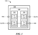
- FIG. 1 shows an example of a signal isolator 100 including first and second dies 102, 104 that form part of an integrated circuit package 106 having magnetic signal latching in accordance with example embodiments of the invention.
- the IC package 106 includes a first input signal INA connected to the first die 102 and a first output signal OUTA connected to the second die 104.
- the IC package 106 further includes a second input signal INB connected to the second die 104 and a second output signal OUTB to the first die 104.
- the first and second dies 102, 104 are separated by a barrier region 108, such as an isolation barrier.
- the first die 102 includes a first transmit module 110 and the second die includes a first receive module 112 that provides a signal path from the first input signal INA to the first output signal OUTA across the barrier 108.
- the second die 104 includes a second transmit module 114 and the first die 104 includes a second receive module 116 that provides a signal path from the second input signal INB to the second output signal OUTB across the barrier 108.
- any practical number of transmit, receive, and transmit/receive modules can be formed on the first and/or second die to meet the needs of a particular application. It is further understood that transmit, receive, and transmit/receive modules can comprise the same or different components.
- bi-directional communication is provided across the barrier.
- circuity in the first and/or second die can be provided to process signals, perform routing of signals, and the like.
- sensing elements are formed in, on, or about the first and/or second die.
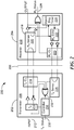
- FIG. 2 shows an example signal isolator 200 having magnetic signal latching of signals from a transmitter 202 to a receiver 204 separated by an isolation barrier 206.
- the transmitter 202 is disposed on a first die 208 and the receiver 204 is disposed on a second die 210, where the first and second die have different voltage domains.
- An INPUT signal 212 is provided to a transmit module 214 that provides a differential output signal to a transmit current latch module 216, which transmits signals in the form of a magnetic signal across the barrier 206 to a receiver Rx module 218.
- the receiver module 218 includes a magnetic field sensing element 220.
- the receiver module 218 includes a bi-stable magnetoresistive element. The receive module 218 provides an OUTPUT signal that can be coupled to an output pin of a signal isolator IC package.
- the receiver 204 includes a receiver echo module 222 coupled to the receiver Rx module 218 that receives the signal sensed by the magnetic field sensing element 220.
- the latched value in the receive current latch module 223 is transmitted in the form of a magnetic signal across the barrier 206 to a transmitter Rx module 226.
- the receiver 204 can generate a receive status signal 228 and the transmitter 202 can generate a transmit status signal 230.
- the transmit module 214 When the INPUT 212 changes state, the transmit module 214 outputs a current pulse representing the INPUT state, creating a magnetic field on the receiver 204.
- the receiver rx module 218 detects the change of state and latches the detected value, which represents the changed state of the data at the INPUT. In order to quickly recover from any data disruption during the data transmission or reception process, a feedback mechanism can be implemented.
- the receiver echo module 222 value latched by the receive current latch module 223 is sent to the transmitter rx module 226 which latches the value and provides this value to a combiner 232.
- the transmit current latch module 216 provides the latched last data transmission sent to the receiver side to the combiner 232, which also receives the INPUT signal 212.
- the combiner is provided as a logical NOR.
- the combiner 232 output is provided to a controller 234, which receives the value in the transmit module 214.
- the transmitter 202 resends a pulse representing the INPUT data state to correct for any inconsistency in the transmitter rx module 226 and the INPUT for setting the OUTPUT equal to the INPUT.
- the isolator latches transmission information at the receiver rx module 218 in magnetic form. Similarly, latching the transmitted data state at the transmitter rx module 226 in magnetic form makes the correction scheme immune to electrical disturbances from the environment.
- the rx echo module 222 can transmit a signal that is an inverse of the state of the receiver rx module 218 periodically as determined by the watch dog timer 224.
- the rx echo module 222 can be triggered by toggling the state of the receiver rx module 218.
- the transmit controller 234 recognizes that the state of the transmitter rx module 226 does not equal the INPUT state and resends the last data transmission.
- the receiver rx module 218 detects the transmission and determines that the transmit side is functioning properly.
- the receiver side echoes the data transition to the transmitter side correcting the state of the transmitter rx module 226 indicating that the receiver side is working properly. If this round trip reset of the data is not completed properly, the transmit status signal 230 and/or the receive status signal 228 can indicate that a fault has occurred.
- FIG. 3 shows an example magnetoresistive sensor 300 having a bridge configuration 302.
- MR elements 304a and 304c will saturate in one direction and MR elements 304b and 304d will saturate in the opposite direction.
- These saturation levels will be latched, i.e. remain in state, until an opposite magnetic field of large enough amplitude overcomes the coercive force of the MR element, as shown in FIG. 4 , changing the state of the MR magnetic latch.
- these opposite states of the magnetorestive sensing elements 304a-d are coupled to an amplifier or comparator 306 to generate an output voltage equal to the latched state of the MR elements.
- FIG. 5A shows example waveforms for an example signal isolator having magnetic signal latching.
- the example waveforms represent the output state of the elements of FIG. 2 .
- waveform Tx CL corresponds to the output of the transmit current latch module 216 in FIG. 2 .
- a transition on the INPUT signal to a logical ONE generates a Tx pulse output by the transmit module 214 is transmitted across the barrier, and is latched during the transmission. This pulse is detected and latched as Rx TMR.
- Rx Echo receives the state of Rx TMR and generates a pulse which is transmitted across the barrier, during which it is latched as Rx CL, for detection and latching as Tx TMR. Since a timeout for the controller was not exceeded, the controller output does not transition.
- the timeout corresponds to a time from a transition of the INPUT signal to a transition of TX TMR.
- FIG. 5B shows example waveforms that have some similarity with FIG. 5A where a controller timeout is exceeded.
- the time from the INPUT signal transitioning to a ONE state to the time the Tx TMR signal (226 in FIG. 2 ) exceeds the timeout value.
- a disruption causes the Tx current pulse in response to the rising edge of the INPUT signal to be missed, so that Tx CL, Rx TMR, Rx Echo signals do not transition, so that the Tx TMR signal monitored by the controller does not transition.
- the controller After the controller detects that the timeout has been exceeded to see state agreement between the INPUT signal and Tx TMR, the controller generates a pulse that causes the transmitter to resend a Tx pulse, which is latched as Tx CL during the transmission, across the barrier to the receiver Rx TMR.
- the Rx Echo signal generates a pulse that is latched as Rx CL during the transmission across the barrier for detection and latching as Tx TMR after which the controller output resets.
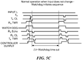
- FIG. 5C shows example waveforms when a watchdog timer signal times out. If the INPUT signal does not transition for a selected amount time, the watchdog timer changes the state of the Rx TMR triggering a signal causing Rx Echo to generate a pulse. In an example embodiment, the rising edge of the watchdog timer signal causes the Rx Echo signal to generate a positive pulse and the falling edge of the watchdog timer signal causes the Rx Echo signal to generate a negative pulse.
- the controller recognizes that the INPUT signal and Tx TMR do not match and generates a pulse that causes the last transmission, here a negative pulse to be resent to the receiver, which is detected by Rx TMR. With reception of this pulse, it can be determined that the transmitter is functioning properly.
- the Rx Echo signal transitions, which causes the Rx CL signal to transition and send a signal to the transmitter.
- the Tx TMR signal transitions indicating that the receiver side is functioning properly.
- the Tx Status and/or Rx Status signals 230, 228 ( FIG. 2 ) can be transitioned to an active state in the event the transmitter and/or receiver is not functioning properly.
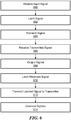
- FIG. 6 shows an example sequence of steps for transmitting a signal with magnetic latching.
- an input is received, such as at an input pin of a signal isolator.
- the input signal is transmitted across a barrier, and latched during the transmission, to a receiver in step 604.
- a magnetoresistive element is used to detect and latch the signal from the transmitter.
- the transmitted signal is received by the receiver.
- the signal can be output by the isolator, such as on an output pin.
- the received signal is transmitted across, and latched during the transmission, the barrier to a sensing element on the transmitter in step 612.
- the sensing element includes a bi-stable magnetoresitive element.
- signals can be examined to determine whether the receiver and/or transmitter are operating properly.
- the transmitter examines the input signal, the latched input signal, and the latched received signal from the receiver. If signals do not match, a controller can retransmit a signal to the receiver.
- a watchdog timer can be used to determine proper operation when data is not being sent.
- the current latch used to detect the transmission of the magnetic field to the other side of the barrier can also be used to detect other current sources on chip.
- it can be used to detect the input current or output drive current; or it could be used to detect current flowing in a shield, or any current needed to be detected as a circuit element as part of a design.
- the magnetic field sensing elements can comprise any suitable magnetoresistive technologies, including AMR, GMR, TMR, or other magneto-resistive technology.
- Example transmissions can be provided as pulsed current, direct current, continuous frequency (e.g., On-off-Keying or OOK) or other suitable data transmission method.
- each die can have any combination of drivers and receivers and each driver and receiver data transmission channel can share any of the fast recovery or diagnostic features or have such features for each individual data channel.
- outputs can be in buffered with a push-pull, open drain or other such output driver, or the output can be a magneto-resistive device with change in resistance indicating logic states.
- Signal isolators in accordance with example embodiments that transmit data across the isolation barrier using pulses to encode data state transitions have low quiescent and data transmission power consumption.
- Conventional signal isolators that use pulses to encode data transitions tend to be prone to output data errors where the output data state does not follow the input data state during the occurrence of electrical disturbances.
- the disturbances can be created by any one of many different electrical phenomenon that can disrupt the data state that is latched at the receiver side by an electrical circuit that holds the data state. The external disturbance can cause the electric circuit latch to change states.
- the digital data is preserved on the transmitter and receiver side during external events that disrupt the electrical operation of the transmitter or receiver making it more immune to disturbance by external electrical phenomenon than other isolator technologies.
- echo feedback in example embodiments of the invention ensures that if the transmission pulse is missed or the receiver pulse is missed during an electrical disturbance the data output is quickly set equal to the data input, while having the benefit of low power consumption and quick data recovery.
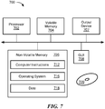
- FIG. 7 shows an exemplary computer 700 that can perform at least part of the processing described herein.
- the computer 700 includes a processor 702, a volatile memory 704, a non-volatile memory 706 (e.g., hard disk), an output device 707 and a graphical user interface (GUI) 708 (e.g., a mouse, a keyboard, a display, for example).
- the non-volatile memory 706 stores computer instructions 712, an operating system 716 and data 718.
- the computer instructions 712 are executed by the processor 702 out of volatile memory 704.
- an article 720 comprises non-transitory computer-readable instructions.
- Processing may be implemented in hardware, software, or a combination of the two. Processing may be implemented in computer programs executed on programmable computers/machines that each includes a processor, a storage medium or other article of manufacture that is readable by the processor (including volatile and non-volatile memory and/or storage elements), at least one input device, and one or more output devices. Program code may be applied to data entered using an input device to perform processing and to generate output information.
- Processing may be performed by one or more programmable processors executing one or more computer programs to perform the functions of the system. All or part of the system may be implemented as, special purpose logic circuitry (e.g., an FPGA (field programmable gate array) and/or an ASIC (application-specific integrated circuit)).
- special purpose logic circuitry e.g., an FPGA (field programmable gate array) and/or an ASIC (application-specific integrated circuit)
Landscapes
- Engineering & Computer Science (AREA)
- Computer Networks & Wireless Communication (AREA)
- Signal Processing (AREA)
- Physics & Mathematics (AREA)
- Power Engineering (AREA)
- Condensed Matter Physics & Semiconductors (AREA)
- General Physics & Mathematics (AREA)
- Electromagnetism (AREA)
- Measuring Magnetic Variables (AREA)
- Electronic Switches (AREA)
Abstract
Description
- As is known in the art, signal isolators can be used to transfer information across a barrier used to separate voltage domains for safety or functional isolation. For example, optocouplers include a LED that emits light through an optically transparent insulating film and strikes a photo detector that generates a current flow that corresponds to the emitted light. RF carriers can also be used to transmit information across an isolation barrier.
- The present invention provides methods and apparatus for a signal isolator having magnetoresistive elements to latch information. In embodiments, data is transmitted across the isolation barrier as a magnetic field and received by a by magnetoresistive structure. By latching data magnetically, the signal isolator will recover relatively quickly from any one of many forms of electrical interference that may disrupt the data transfer. In embodiments, the signal isolator may monitor data transmission and reception across the isolation barrier. In some embodiments, a signal isolator indicates on one or both sides of the barrier whether the isolator is operating properly.
- In one aspect, a signal isolator comprises: a transmitter comprising: a transmit module to receive an input signal; and a transmit current latching module to magnetically latch an output of the transmit module; and a receiver comprising: a receive module including a receiver magnetic field sensing element to detect and magnetically latch a current signal from the transmit current latching module.
- A signal isolator can further include one or more of the following features: the transmit module further includes a transmitter receive module to receive signals from the receiver, the receiver further includes: a receiver echo module coupled to the receiver magnetic field sensing element; and a receive current latching module to receive an output of the receiver echo module and transmit an output to the transmitter receive module, a barrier region between the transmitter and the receiver, the transmitter and the receiver are disposed on separate die, the receiver magnetic field sensing element includes a magnetoresitive element, the magnetoresistive element comprises a bi-stable magnetoresistive element, the transmit module includes a controller, the controller monitors a state of the input signal, the transmit current latching module, and a transmitter receive module, the controller is configured to resend a signal from the transmitter to the receiver when a disruption of the input signal is detected, the disruption is detected when a timeout is exceeded, and/or a watchdog timer coupled to a receive echo module to detect faults in the receiver module and/or transmit module when data signals are not present.
- In another aspect, a method of communicating signals from a transmitter to a receiver isolated from the transmitter comprises: employing a transmitter having a transmit module to receive an input signal and a transmit current latching module to magnetically latch an output of the transmit module; and employing a receiver having a receive module including a receiver magnetic field sensing element to detect and magnetically latch a signal from the transmit current latching module.
- A method can further include one or more of the following features: the transmit module further includes a transmitter receive module to receive signals from the receiver, the receiver further includes: a receiver echo module coupled to the receiver magnetic field sensing element; and a receive current latching module to receive an output of the receiver echo module and transmit an output to the transmitter receive module, employing a barrier region between the transmitter and the receiver, the transmitter and the receiver are disposed on separate die, the receiver magnetic field sensing element includes a magnetoresitive element, the magnetoresistive element comprises a bi-stable magnetoresistive element, employing a controller to monitor a state of the input signal, the transmit current latching module, and a transmitter receive module, the controller is configured to resend a signal from the transmitter to the receiver when a disruption of the input signal is detected, the disruption is detected when a timeout is exceeded, and/or employing a watchdog timer coupled to a receive echo module to detect faults in the receiver module and/or transmit module when data signals are not present.
- In a further aspect, a signal isolator comprises: a transmitter comprising: a transmit means to receive an input signal; and a transmit current latching means to magnetically latch an output of the transmit means; and a receiver comprising: a receive means including a receiver magnetic field sensing means for detecting and magnetically latching a signal from the transmit latching means.
- The foregoing features of this invention, as well as the invention itself, may be more fully understood from the following description of the drawings in which:
-
FIG. 1 is a schematic representation of a signal isolator having magnetic signal latching in accordance with example embodiments of the invention; -
FIG. 2 is a schematic representation of a signal isolator having magnetic signal latching in accordance with example embodiments of the invention; -
FIG. 3 is a schematic representation of an example magnetic field sensing element that can form a portion of the signal isolator ofFIG. 2 ; -
FIG. 4 is a waveform diagram of an example signal for the magnetic field sensing element ofFIG. 3 ; -
FIG. 5A is waveform diagram of example signals generated by an illustrative signal isolator in a first mode; -
FIG. 5B is waveform diagram of example signals generated by an illustrative signal isolator in a second mode; -
FIG. 5C is waveform diagram of example signals generated by an illustrative signal isolator in a third mode; -
FIG. 6 is a flow diagram showing an example sequence of steps for a signal isolator; -
FIG. 7 is a schematic representation of an example computer that may perform at least a portion of the processing described herein. -
FIG. 1 shows an example of asignal isolator 100 including first andsecond dies integrated circuit package 106 having magnetic signal latching in accordance with example embodiments of the invention. In an embodiment, theIC package 106 includes a first input signal INA connected to thefirst die 102 and a first output signal OUTA connected to thesecond die 104. TheIC package 106 further includes a second input signal INB connected to thesecond die 104 and a second output signal OUTB to thefirst die 104. The first andsecond dies barrier region 108, such as an isolation barrier. - In embodiments, the
first die 102 includes afirst transmit module 110 and the second die includes afirst receive module 112 that provides a signal path from the first input signal INA to the first output signal OUTA across thebarrier 108. Thesecond die 104 includes asecond transmit module 114 and thefirst die 104 includes asecond receive module 116 that provides a signal path from the second input signal INB to the second output signal OUTB across thebarrier 108. - It is understood that any practical number of transmit, receive, and transmit/receive modules can be formed on the first and/or second die to meet the needs of a particular application. It is further understood that transmit, receive, and transmit/receive modules can comprise the same or different components. In addition, in embodiments, bi-directional communication is provided across the barrier. Further, circuity in the first and/or second die can be provided to process signals, perform routing of signals, and the like. In some embodiments, sensing elements are formed in, on, or about the first and/or second die.
-
FIG. 2 shows anexample signal isolator 200 having magnetic signal latching of signals from atransmitter 202 to areceiver 204 separated by anisolation barrier 206. In embodiments, thetransmitter 202 is disposed on afirst die 208 and thereceiver 204 is disposed on asecond die 210, where the first and second die have different voltage domains. - An
INPUT signal 212 is provided to atransmit module 214 that provides a differential output signal to a transmitcurrent latch module 216, which transmits signals in the form of a magnetic signal across thebarrier 206 to areceiver Rx module 218. In embodiments, thereceiver module 218 includes a magneticfield sensing element 220. In embodiments, thereceiver module 218 includes a bi-stable magnetoresistive element. The receivemodule 218 provides an OUTPUT signal that can be coupled to an output pin of a signal isolator IC package. - While example embodiments are shown as transmitting differential signals, in other embodiments non-differential signals are transmitted and received. It is understood that any suitable signal transmission configuration can be used.
- In embodiments, the
receiver 204 includes areceiver echo module 222 coupled to thereceiver Rx module 218 that receives the signal sensed by the magneticfield sensing element 220. The latched value in the receivecurrent latch module 223 is transmitted in the form of a magnetic signal across thebarrier 206 to atransmitter Rx module 226. As described more fully below, thereceiver 204 can generate areceive status signal 228 and thetransmitter 202 can generate atransmit status signal 230. - While a signal channel is shown, it is understood that additional channels in either direction can be added to meet the needs of a particular application.
- When the
INPUT 212 changes state, thetransmit module 214 outputs a current pulse representing the INPUT state, creating a magnetic field on thereceiver 204. In embodiments, thereceiver rx module 218 detects the change of state and latches the detected value, which represents the changed state of the data at the INPUT. In order to quickly recover from any data disruption during the data transmission or reception process, a feedback mechanism can be implemented. - The
receiver echo module 222 value latched by the receivecurrent latch module 223 is sent to thetransmitter rx module 226 which latches the value and provides this value to acombiner 232. The transmitcurrent latch module 216 provides the latched last data transmission sent to the receiver side to thecombiner 232, which also receives theINPUT signal 212. In one particular embodiment, the combiner is provided as a logical NOR. Thecombiner 232 output is provided to acontroller 234, which receives the value in thetransmit module 214. - If either the transmit
current latch module 216 value or thetransmitter rx module 226 value do not agree with the INPUT, then the OUTPUT could be different than the INPUT. In an example embodiment, thetransmitter 202 resends a pulse representing the INPUT data state to correct for any inconsistency in thetransmitter rx module 226 and the INPUT for setting the OUTPUT equal to the INPUT. - In order to make the OUTPUT immune to electrical disruptions that can disturb the data state at the OUTPUT, the isolator latches transmission information at the
receiver rx module 218 in magnetic form. Similarly, latching the transmitted data state at thetransmitter rx module 226 in magnetic form makes the correction scheme immune to electrical disturbances from the environment. - In embodiments, in order to be able to distinguish between no data state changes and a non-functional transmitter or receiver device, the
rx echo module 222 can transmit a signal that is an inverse of the state of thereceiver rx module 218 periodically as determined by thewatch dog timer 224. Therx echo module 222 can be triggered by toggling the state of thereceiver rx module 218. When the transmission from therx echo module 222 is detected by thetransmitter rx module 226, the transmitcontroller 234 recognizes that the state of thetransmitter rx module 226 does not equal the INPUT state and resends the last data transmission. Thereceiver rx module 218 detects the transmission and determines that the transmit side is functioning properly. The receiver side echoes the data transition to the transmitter side correcting the state of thetransmitter rx module 226 indicating that the receiver side is working properly. If this round trip reset of the data is not completed properly, the transmitstatus signal 230 and/or the receivestatus signal 228 can indicate that a fault has occurred. -
FIG. 3 shows anexample magnetoresistive sensor 300 having abridge configuration 302.MR elements MR elements FIG. 4 , changing the state of the MR magnetic latch. In the illustrative embodiments, these opposite states of themagnetorestive sensing elements 304a-d are coupled to an amplifier orcomparator 306 to generate an output voltage equal to the latched state of the MR elements. -
FIG. 5A shows example waveforms for an example signal isolator having magnetic signal latching. The example waveforms represent the output state of the elements ofFIG. 2 . For example, waveform Tx CL corresponds to the output of the transmitcurrent latch module 216 inFIG. 2 . As can be seen, a transition on the INPUT signal to a logical ONE generates a Tx pulse output by the transmitmodule 214 is transmitted across the barrier, and is latched during the transmission. This pulse is detected and latched as Rx TMR. Rx Echo receives the state of Rx TMR and generates a pulse which is transmitted across the barrier, during which it is latched as Rx CL, for detection and latching as Tx TMR. Since a timeout for the controller was not exceeded, the controller output does not transition. In embodiments, the timeout corresponds to a time from a transition of the INPUT signal to a transition of TX TMR. -
FIG. 5B shows example waveforms that have some similarity withFIG. 5A where a controller timeout is exceeded. In the illustrated sequence, the time from the INPUT signal transitioning to a ONE state to the time the Tx TMR signal (226 inFIG. 2 ) exceeds the timeout value. For example, a disruption causes the Tx current pulse in response to the rising edge of the INPUT signal to be missed, so that Tx CL, Rx TMR, Rx Echo signals do not transition, so that the Tx TMR signal monitored by the controller does not transition. After the controller detects that the timeout has been exceeded to see state agreement between the INPUT signal and Tx TMR, the controller generates a pulse that causes the transmitter to resend a Tx pulse, which is latched as Tx CL during the transmission, across the barrier to the receiver Rx TMR. The Rx Echo signal generates a pulse that is latched as Rx CL during the transmission across the barrier for detection and latching as Tx TMR after which the controller output resets. -
FIG. 5C shows example waveforms when a watchdog timer signal times out. If the INPUT signal does not transition for a selected amount time, the watchdog timer changes the state of the Rx TMR triggering a signal causing Rx Echo to generate a pulse. In an example embodiment, the rising edge of the watchdog timer signal causes the Rx Echo signal to generate a positive pulse and the falling edge of the watchdog timer signal causes the Rx Echo signal to generate a negative pulse. - The controller recognizes that the INPUT signal and Tx TMR do not match and generates a pulse that causes the last transmission, here a negative pulse to be resent to the receiver, which is detected by Rx TMR. With reception of this pulse, it can be determined that the transmitter is functioning properly. The Rx Echo signal transitions, which causes the Rx CL signal to transition and send a signal to the transmitter. Upon detection, the Tx TMR signal transitions indicating that the receiver side is functioning properly. The Tx Status and/or Rx Status signals 230, 228 (
FIG. 2 ) can be transitioned to an active state in the event the transmitter and/or receiver is not functioning properly. -
FIG. 6 shows an example sequence of steps for transmitting a signal with magnetic latching. Instep 600, an input is received, such as at an input pin of a signal isolator. Instep 602, the input signal is transmitted across a barrier, and latched during the transmission, to a receiver instep 604. In embodiments, a magnetoresistive element is used to detect and latch the signal from the transmitter. Instep 606, the transmitted signal is received by the receiver. Instep 608, the signal can be output by the isolator, such as on an output pin. - In
step 610, the received signal is transmitted across, and latched during the transmission, the barrier to a sensing element on the transmitter instep 612. In embodiments, the sensing element includes a bi-stable magnetoresitive element. Instep 614, signals can be examined to determine whether the receiver and/or transmitter are operating properly. In one embodiment, the transmitter examines the input signal, the latched input signal, and the latched received signal from the receiver. If signals do not match, a controller can retransmit a signal to the receiver. In embodiments, a watchdog timer can be used to determine proper operation when data is not being sent. - In a further embodiment, the current latch used to detect the transmission of the magnetic field to the other side of the barrier, can also be used to detect other current sources on chip. For example it can be used to detect the input current or output drive current; or it could be used to detect current flowing in a shield, or any current needed to be detected as a circuit element as part of a design.
- It is understood that the magnetic field sensing elements can comprise any suitable magnetoresistive technologies, including AMR, GMR, TMR, or other magneto-resistive technology. Example transmissions can be provided as pulsed current, direct current, continuous frequency (e.g., On-off-Keying or OOK) or other suitable data transmission method.
- While example embodiments are shown having a transmitter and receiver on separate die, in other embodiments, they are on the same die. In addition, each die can have any combination of drivers and receivers and each driver and receiver data transmission channel can share any of the fast recovery or diagnostic features or have such features for each individual data channel. In embodiments, outputs can be in buffered with a push-pull, open drain or other such output driver, or the output can be a magneto-resistive device with change in resistance indicating logic states.
- Signal isolators in accordance with example embodiments that transmit data across the isolation barrier using pulses to encode data state transitions have low quiescent and data transmission power consumption. Conventional signal isolators that use pulses to encode data transitions tend to be prone to output data errors where the output data state does not follow the input data state during the occurrence of electrical disturbances. The disturbances can be created by any one of many different electrical phenomenon that can disrupt the data state that is latched at the receiver side by an electrical circuit that holds the data state. The external disturbance can cause the electric circuit latch to change states.
- Known digital isolators that use on-off keying recover quickly from data disturbances by continuous data transmission across the barrier which requires high power consumption during one of the data states when a signal is being continuously transmitted across the isolation barrier. When using on-off keying, the data state when the frequency transmission is off cannot be distinguished from a transmitter that is non-functional.
- By using a magneto-resistive latch to hold the data state on the receiver side in accordance with example embodiments of the invention, the digital data is preserved on the transmitter and receiver side during external events that disrupt the electrical operation of the transmitter or receiver making it more immune to disturbance by external electrical phenomenon than other isolator technologies. In addition, echo feedback in example embodiments of the invention ensures that if the transmission pulse is missed or the receiver pulse is missed during an electrical disturbance the data output is quickly set equal to the data input, while having the benefit of low power consumption and quick data recovery.
-
FIG. 7 shows anexemplary computer 700 that can perform at least part of the processing described herein. Thecomputer 700 includes aprocessor 702, avolatile memory 704, a non-volatile memory 706 (e.g., hard disk), anoutput device 707 and a graphical user interface (GUI) 708 (e.g., a mouse, a keyboard, a display, for example). Thenon-volatile memory 706stores computer instructions 712, anoperating system 716 anddata 718. In one example, thecomputer instructions 712 are executed by theprocessor 702 out ofvolatile memory 704. In one embodiment, anarticle 720 comprises non-transitory computer-readable instructions. - Processing may be implemented in hardware, software, or a combination of the two. Processing may be implemented in computer programs executed on programmable computers/machines that each includes a processor, a storage medium or other article of manufacture that is readable by the processor (including volatile and non-volatile memory and/or storage elements), at least one input device, and one or more output devices. Program code may be applied to data entered using an input device to perform processing and to generate output information.
- Processing may be performed by one or more programmable processors executing one or more computer programs to perform the functions of the system. All or part of the system may be implemented as, special purpose logic circuitry (e.g., an FPGA (field programmable gate array) and/or an ASIC (application-specific integrated circuit)).
- Having described exemplary embodiments of the invention, it will now become apparent to one of ordinary skill in the art that other embodiments incorporating their concepts may also be used. The embodiments contained herein should not be limited to disclosed embodiments but rather should be limited only by the spirit and scope of the appended claims. All publications and references cited herein are expressly incorporated herein by reference in their entirety.
- Elements of different embodiments described herein may be combined to form other embodiments not specifically set forth above. Various elements, which are described in the context of a single embodiment, may also be provided separately or in any suitable subcombination. Other embodiments not specifically described herein are also within the scope of the following claims.
Claims (26)
- A signal isolator, comprising:a transmitter comprising:a transmit module to receive an input signal; anda transmit current latching module to magnetically latch an output of the transmit module; anda receiver comprising:a receive module including a receiver magnetic field sensing element to detect and magnetically latch a signal from the transmit current latching module.
- The signal isolator according to claim 1, wherein the transmit module further includes a transmitter receive module to receive signals from the receiver.
- The signal isolator according to claim 2, wherein the receiver further includes:a receiver echo module coupled to the receiver magnetic field sensing element; anda receive current latching module to receive an output of the receiver echo module and transmit an output to the transmitter receive module.
- The signal isolator according to claim 1, further comprising a barrier region between the transmitter and the receiver.
- The signal isolator according to claim 1, wherein the transmitter and the receiver are disposed on separate die.
- The signal isolator according to claim 1, wherein the receiver magnetic field sensing element includes a magnetoresitive element.
- The signal isolator according to claim 6, wherein the magnetoresistive element comprises a bi-stable magnetoresistive element.
- The signal isolator according to claim 1, wherein the transmit module includes a controller.
- The signal isolator according to claim 8, wherein the controller monitors a state of the input signal, the transmit current latching module, and a transmitter receive module.
- The signal isolator according to claim 9, wherein the controller is configured to resend a signal from the transmitter to the receiver when a disruption of the input signal is detected.
- The signal isolator according to claim 10, wherein the disruption is detected when a timeout is exceeded.
- The signal isolator according to claim 1, further including a watchdog timer coupled to a receive echo module to detect faults in the receiver module and/or transmit module when data signals are not present.
- A method of communicating signals from a transmitter to a receiver isolated from the transmitter, comprising:employing a transmitter having a transmit module to receive an input signal and a transmit current latching module to magnetically latch an output of the transmit module; andemploying a receiver having a receive module including a receiver magnetic field sensing element to detect and magnetically latch a signal from the transmit current latching module.
- The method to claim 13, wherein the transmit module further includes a transmitter receive module to receive signals from the receiver.
- The method according to claim 14, wherein the receiver further includes:a receiver echo module coupled to the receiver magnetic field sensing element; anda receive current latching module to receive an output of the receiver echo module and transmit an output to the transmitter receive module.
- The method according to claim 13, further employing a barrier region between the transmitter and the receiver.
- The method according to claim 13, wherein the transmitter and the receiver are disposed on separate die.
- The method according to claim 13, wherein the receiver magnetic field sensing element includes a magnetoresitive element.
- The method according to claim 18, wherein the magnetoresistive element comprises a bi-stable magnetoresistive element.
- The method according to claim 13, further including employing a controller to monitor a state of the input signal, the transmit current latching module, and a transmitter receive module.
- The method according to claim 20, wherein the controller is configured to resend a signal from the transmitter to the receiver when a disruption of the input signal is detected.
- The method according to claim 21, wherein the disruption is detected when a timeout is exceeded.
- The method according to claim 13, further including employing a watchdog timer coupled to a receive echo module to detect faults in the receiver module and/or transmit module when data signals are not present.
- A signal isolator, comprising:a transmitter comprising:a transmit means to receive an input signal; anda transmit current latching means to magnetically latch an output of the transmit means; anda receiver comprising:a receive means including a receiver magnetic field sensing means for detecting and magnetically latching a signal from the transmit latching means.
- The signal isolator according to claim 24, wherein the transmit means further includes a transmitter receive means for receiving signals from the receiver.
- The signal isolator according to claim 24, wherein the receiver further includes:a receiver echo means coupled to the receiver magnetic field sensing means; anda receive current latching means for receiving an output of the receiver echo means and transmitting an output to the transmitter receive means.
Applications Claiming Priority (1)
| Application Number | Priority Date | Filing Date | Title |
|---|---|---|---|
| US15/801,679 US10236932B1 (en) | 2017-11-02 | 2017-11-02 | Signal isolator having magnetic signal latching |
Publications (2)
| Publication Number | Publication Date |
|---|---|
| EP3481018A1 true EP3481018A1 (en) | 2019-05-08 |
| EP3481018B1 EP3481018B1 (en) | 2023-11-08 |
Family
ID=64100574
Family Applications (1)
| Application Number | Title | Priority Date | Filing Date |
|---|---|---|---|
| EP18202972.8A Active EP3481018B1 (en) | 2017-11-02 | 2018-10-26 | Signal isolator having magnetic signal latching |
Country Status (2)
| Country | Link |
|---|---|
| US (2) | US10236932B1 (en) |
| EP (1) | EP3481018B1 (en) |
Families Citing this family (7)
| Publication number | Priority date | Publication date | Assignee | Title |
|---|---|---|---|---|
| US11115244B2 (en) * | 2019-09-17 | 2021-09-07 | Allegro Microsystems, Llc | Signal isolator with three state data transmission |
| TWI737529B (en) * | 2020-10-30 | 2021-08-21 | 精拓科技股份有限公司 | Digital isolator |
| US11885646B2 (en) | 2021-08-12 | 2024-01-30 | Allegro Microsystems, Llc | Programmable active pixel test injection |
| US12306701B2 (en) | 2022-03-30 | 2025-05-20 | Allegro Microsystems, Llc | Data stream watchdog injection |
| US11722141B1 (en) | 2022-04-22 | 2023-08-08 | Allegro Microsystems, Llc | Delay-locked-loop timing error mitigation |
| US12199586B2 (en) | 2023-03-30 | 2025-01-14 | Allegro Microsystems, Llc | Capacitive isolator having common mode noise suppression |
| US12526012B1 (en) | 2024-09-26 | 2026-01-13 | Allegro Microsystems, Llc | Wireless power transmission with channel redundancy |
Citations (4)
| Publication number | Priority date | Publication date | Assignee | Title |
|---|---|---|---|---|
| US20020135236A1 (en) * | 1997-10-23 | 2002-09-26 | Haigh Geoffrey T. | Non-optical signal isolator |
| US20150004902A1 (en) * | 2013-06-28 | 2015-01-01 | John M. Pigott | Die-to-die inductive communication devices and methods |
| US20170207655A1 (en) * | 2016-01-19 | 2017-07-20 | Industrial Technology Research Institute | Galvanic isolator circuit |
| EP3293888A1 (en) * | 2016-09-13 | 2018-03-14 | Allegro Microsystems, LLC | Signal isolator having bidirectional communication between die |
Family Cites Families (20)
| Publication number | Priority date | Publication date | Assignee | Title |
|---|---|---|---|---|
| US4399557A (en) * | 1981-12-15 | 1983-08-16 | Motorola Inc. | Minimum power, feedback controller, transmit/receive switch |
| US5831426A (en) * | 1996-08-16 | 1998-11-03 | Nonvolatile Electronics, Incorporated | Magnetic current sensor |
| US6054780A (en) * | 1997-10-23 | 2000-04-25 | Analog Devices, Inc. | Magnetically coupled signal isolator using a Faraday shielded MR or GMR receiving element |
| US6300617B1 (en) * | 1998-03-04 | 2001-10-09 | Nonvolatile Electronics, Incorporated | Magnetic digital signal coupler having selected/reversal directions of magnetization |
| US7259545B2 (en) | 2003-02-11 | 2007-08-21 | Allegro Microsystems, Inc. | Integrated sensor |
| US7768083B2 (en) | 2006-01-20 | 2010-08-03 | Allegro Microsystems, Inc. | Arrangements for an integrated sensor |
| ITTO20070325A1 (en) * | 2007-05-11 | 2008-11-12 | St Microelectronics Srl | INTEGRATED GALVANIC INSULATOR USING WIRELESS TRANSMISSION |
| US7973527B2 (en) | 2008-07-31 | 2011-07-05 | Allegro Microsystems, Inc. | Electronic circuit configured to reset a magnetoresistance element |
| US8063634B2 (en) | 2008-07-31 | 2011-11-22 | Allegro Microsystems, Inc. | Electronic circuit and method for resetting a magnetoresistance element |
| EP2393888B1 (en) | 2009-02-03 | 2015-06-03 | Hewlett-Packard Development Company, L.P. | An inkjet ink including polyurethane |
| EP2280488A1 (en) * | 2009-06-30 | 2011-02-02 | STMicroelectronics S.r.l. | Transmission and reception apparatus for digital signals |
| JP5681892B2 (en) * | 2010-02-19 | 2015-03-11 | パナソニックIpマネジメント株式会社 | Electronics |
| JP5622328B2 (en) * | 2011-03-25 | 2014-11-12 | パナソニック株式会社 | Electronic device with gripping device |
| JP5538460B2 (en) * | 2011-04-06 | 2014-07-02 | パナソニック株式会社 | Expansion device and information processing system including the same |
| KR101097649B1 (en) * | 2011-05-06 | 2011-12-22 | 김영선 | Handle structure of portable terminal |
| JP5448216B1 (en) * | 2012-09-26 | 2014-03-19 | Necインフロンティア株式会社 | Portable information terminal holder and desk phone |
| JP5870317B2 (en) * | 2013-02-14 | 2016-02-24 | パナソニックIpマネジメント株式会社 | Mobile device |
| JPWO2014133066A1 (en) * | 2013-02-28 | 2017-02-02 | 日本電気株式会社 | COMMUNICATION SYSTEM, TERMINAL, COMMUNICATION CONTROL DEVICE, COMMUNICATION METHOD, AND PROGRAM |
| US9287917B1 (en) * | 2015-02-19 | 2016-03-15 | A.G. Findings & Mfg. Co. | Electronic device protective case with convenience features |
| EP3116179B1 (en) * | 2015-07-08 | 2018-06-13 | Power Integrations Switzerland GmbH | Communicating across galvanic isolation, for example, in a power converter |
-
2017
- 2017-11-02 US US15/801,679 patent/US10236932B1/en active Active
-
2018
- 2018-10-26 EP EP18202972.8A patent/EP3481018B1/en active Active
-
2019
- 2019-01-24 US US16/256,215 patent/US10498384B2/en active Active
Patent Citations (4)
| Publication number | Priority date | Publication date | Assignee | Title |
|---|---|---|---|---|
| US20020135236A1 (en) * | 1997-10-23 | 2002-09-26 | Haigh Geoffrey T. | Non-optical signal isolator |
| US20150004902A1 (en) * | 2013-06-28 | 2015-01-01 | John M. Pigott | Die-to-die inductive communication devices and methods |
| US20170207655A1 (en) * | 2016-01-19 | 2017-07-20 | Industrial Technology Research Institute | Galvanic isolator circuit |
| EP3293888A1 (en) * | 2016-09-13 | 2018-03-14 | Allegro Microsystems, LLC | Signal isolator having bidirectional communication between die |
Also Published As
| Publication number | Publication date |
|---|---|
| US10236932B1 (en) | 2019-03-19 |
| EP3481018B1 (en) | 2023-11-08 |
| US20190173514A1 (en) | 2019-06-06 |
| US10498384B2 (en) | 2019-12-03 |
Similar Documents
| Publication | Publication Date | Title |
|---|---|---|
| US10498384B2 (en) | Signal isolator having magnetic signal latching | |
| US10142052B2 (en) | Methods and apparatus for communication over an isolation barrier with monitoring | |
| EP3293888B1 (en) | Signal isolator having bidirectional communication between die | |
| JP5930025B2 (en) | USB isolator integrated circuit with USB 2.0 high speed mode and automatic speed detection | |
| EP2996247B1 (en) | Demodulation of on-off-key modulated signals in signal isolator systems | |
| US8497700B2 (en) | Systems and methods for propagating digital data across an isolation barrier | |
| US9678919B2 (en) | Collision detection in EIA-485 bus systems | |
| CN107204610B (en) | Drive circuit | |
| TW202120944A (en) | Testing device and testing method | |
| EP3916406B1 (en) | Integrity monitoring for input/output (io) circuits of a sytsem on a chip (soc) | |
| US9407319B2 (en) | Fault tolerant transceiver | |
| TW202129641A (en) | Serial data processing device and data offset calibration method | |
| US20160336844A1 (en) | Insulation communication device | |
| CN108631808B (en) | Apparatus and method for digital signal transmission | |
| US10574514B2 (en) | Duplex control device and duplex system | |
| US12328119B2 (en) | Transmission circuit | |
| KR101854970B1 (en) | Apparatus and method of multi level reception from pulse-width modulation by using cmos image sensor | |
| EP3157219B1 (en) | Demodulation of on-off modulated signals in signal isolator systems | |
| JP2016116096A (en) | Isolator |
Legal Events
| Date | Code | Title | Description |
|---|---|---|---|
| PUAI | Public reference made under article 153(3) epc to a published international application that has entered the european phase |
Free format text: ORIGINAL CODE: 0009012 |
|
| STAA | Information on the status of an ep patent application or granted ep patent |
Free format text: STATUS: THE APPLICATION HAS BEEN PUBLISHED |
|
| AK | Designated contracting states |
Kind code of ref document: A1 Designated state(s): AL AT BE BG CH CY CZ DE DK EE ES FI FR GB GR HR HU IE IS IT LI LT LU LV MC MK MT NL NO PL PT RO RS SE SI SK SM TR |
|
| AX | Request for extension of the european patent |
Extension state: BA ME |
|
| STAA | Information on the status of an ep patent application or granted ep patent |
Free format text: STATUS: REQUEST FOR EXAMINATION WAS MADE |
|
| 17P | Request for examination filed |
Effective date: 20191108 |
|
| RBV | Designated contracting states (corrected) |
Designated state(s): AL AT BE BG CH CY CZ DE DK EE ES FI FR GB GR HR HU IE IS IT LI LT LU LV MC MK MT NL NO PL PT RO RS SE SI SK SM TR |
|
| STAA | Information on the status of an ep patent application or granted ep patent |
Free format text: STATUS: EXAMINATION IS IN PROGRESS |
|
| 17Q | First examination report despatched |
Effective date: 20200721 |
|
| GRAP | Despatch of communication of intention to grant a patent |
Free format text: ORIGINAL CODE: EPIDOSNIGR1 |
|
| STAA | Information on the status of an ep patent application or granted ep patent |
Free format text: STATUS: GRANT OF PATENT IS INTENDED |
|
| INTG | Intention to grant announced |
Effective date: 20230626 |
|
| GRAS | Grant fee paid |
Free format text: ORIGINAL CODE: EPIDOSNIGR3 |
|
| GRAA | (expected) grant |
Free format text: ORIGINAL CODE: 0009210 |
|
| STAA | Information on the status of an ep patent application or granted ep patent |
Free format text: STATUS: THE PATENT HAS BEEN GRANTED |
|
| AK | Designated contracting states |
Kind code of ref document: B1 Designated state(s): AL AT BE BG CH CY CZ DE DK EE ES FI FR GB GR HR HU IE IS IT LI LT LU LV MC MK MT NL NO PL PT RO RS SE SI SK SM TR |
|
| REG | Reference to a national code |
Ref country code: GB Ref legal event code: FG4D |
|
| REG | Reference to a national code |
Ref country code: CH Ref legal event code: EP |
|
| REG | Reference to a national code |
Ref country code: DE Ref legal event code: R096 Ref document number: 602018060732 Country of ref document: DE |
|
| REG | Reference to a national code |
Ref country code: IE Ref legal event code: FG4D |
|
| REG | Reference to a national code |
Ref country code: LT Ref legal event code: MG9D |
|
| REG | Reference to a national code |
Ref country code: NL Ref legal event code: MP Effective date: 20231108 |
|
| PG25 | Lapsed in a contracting state [announced via postgrant information from national office to epo] |
Ref country code: GR Free format text: LAPSE BECAUSE OF FAILURE TO SUBMIT A TRANSLATION OF THE DESCRIPTION OR TO PAY THE FEE WITHIN THE PRESCRIBED TIME-LIMIT Effective date: 20240209 |
|
| PG25 | Lapsed in a contracting state [announced via postgrant information from national office to epo] |
Ref country code: IS Free format text: LAPSE BECAUSE OF FAILURE TO SUBMIT A TRANSLATION OF THE DESCRIPTION OR TO PAY THE FEE WITHIN THE PRESCRIBED TIME-LIMIT Effective date: 20240308 |
|
| PG25 | Lapsed in a contracting state [announced via postgrant information from national office to epo] |
Ref country code: LT Free format text: LAPSE BECAUSE OF FAILURE TO SUBMIT A TRANSLATION OF THE DESCRIPTION OR TO PAY THE FEE WITHIN THE PRESCRIBED TIME-LIMIT Effective date: 20231108 |
|
| REG | Reference to a national code |
Ref country code: AT Ref legal event code: MK05 Ref document number: 1630637 Country of ref document: AT Kind code of ref document: T Effective date: 20231108 |
|
| PG25 | Lapsed in a contracting state [announced via postgrant information from national office to epo] |
Ref country code: NL Free format text: LAPSE BECAUSE OF FAILURE TO SUBMIT A TRANSLATION OF THE DESCRIPTION OR TO PAY THE FEE WITHIN THE PRESCRIBED TIME-LIMIT Effective date: 20231108 |
|
| PG25 | Lapsed in a contracting state [announced via postgrant information from national office to epo] |
Ref country code: AT Free format text: LAPSE BECAUSE OF FAILURE TO SUBMIT A TRANSLATION OF THE DESCRIPTION OR TO PAY THE FEE WITHIN THE PRESCRIBED TIME-LIMIT Effective date: 20231108 |
|
| PG25 | Lapsed in a contracting state [announced via postgrant information from national office to epo] |
Ref country code: ES Free format text: LAPSE BECAUSE OF FAILURE TO SUBMIT A TRANSLATION OF THE DESCRIPTION OR TO PAY THE FEE WITHIN THE PRESCRIBED TIME-LIMIT Effective date: 20231108 |
|
| PG25 | Lapsed in a contracting state [announced via postgrant information from national office to epo] |
Ref country code: NL Free format text: LAPSE BECAUSE OF FAILURE TO SUBMIT A TRANSLATION OF THE DESCRIPTION OR TO PAY THE FEE WITHIN THE PRESCRIBED TIME-LIMIT Effective date: 20231108 Ref country code: LT Free format text: LAPSE BECAUSE OF FAILURE TO SUBMIT A TRANSLATION OF THE DESCRIPTION OR TO PAY THE FEE WITHIN THE PRESCRIBED TIME-LIMIT Effective date: 20231108 Ref country code: IS Free format text: LAPSE BECAUSE OF FAILURE TO SUBMIT A TRANSLATION OF THE DESCRIPTION OR TO PAY THE FEE WITHIN THE PRESCRIBED TIME-LIMIT Effective date: 20240308 Ref country code: GR Free format text: LAPSE BECAUSE OF FAILURE TO SUBMIT A TRANSLATION OF THE DESCRIPTION OR TO PAY THE FEE WITHIN THE PRESCRIBED TIME-LIMIT Effective date: 20240209 Ref country code: ES Free format text: LAPSE BECAUSE OF FAILURE TO SUBMIT A TRANSLATION OF THE DESCRIPTION OR TO PAY THE FEE WITHIN THE PRESCRIBED TIME-LIMIT Effective date: 20231108 Ref country code: BG Free format text: LAPSE BECAUSE OF FAILURE TO SUBMIT A TRANSLATION OF THE DESCRIPTION OR TO PAY THE FEE WITHIN THE PRESCRIBED TIME-LIMIT Effective date: 20240208 Ref country code: AT Free format text: LAPSE BECAUSE OF FAILURE TO SUBMIT A TRANSLATION OF THE DESCRIPTION OR TO PAY THE FEE WITHIN THE PRESCRIBED TIME-LIMIT Effective date: 20231108 Ref country code: PT Free format text: LAPSE BECAUSE OF FAILURE TO SUBMIT A TRANSLATION OF THE DESCRIPTION OR TO PAY THE FEE WITHIN THE PRESCRIBED TIME-LIMIT Effective date: 20240308 |
|
| PG25 | Lapsed in a contracting state [announced via postgrant information from national office to epo] |
Ref country code: SE Free format text: LAPSE BECAUSE OF FAILURE TO SUBMIT A TRANSLATION OF THE DESCRIPTION OR TO PAY THE FEE WITHIN THE PRESCRIBED TIME-LIMIT Effective date: 20231108 Ref country code: RS Free format text: LAPSE BECAUSE OF FAILURE TO SUBMIT A TRANSLATION OF THE DESCRIPTION OR TO PAY THE FEE WITHIN THE PRESCRIBED TIME-LIMIT Effective date: 20231108 Ref country code: PL Free format text: LAPSE BECAUSE OF FAILURE TO SUBMIT A TRANSLATION OF THE DESCRIPTION OR TO PAY THE FEE WITHIN THE PRESCRIBED TIME-LIMIT Effective date: 20231108 Ref country code: NO Free format text: LAPSE BECAUSE OF FAILURE TO SUBMIT A TRANSLATION OF THE DESCRIPTION OR TO PAY THE FEE WITHIN THE PRESCRIBED TIME-LIMIT Effective date: 20240208 Ref country code: LV Free format text: LAPSE BECAUSE OF FAILURE TO SUBMIT A TRANSLATION OF THE DESCRIPTION OR TO PAY THE FEE WITHIN THE PRESCRIBED TIME-LIMIT Effective date: 20231108 Ref country code: HR Free format text: LAPSE BECAUSE OF FAILURE TO SUBMIT A TRANSLATION OF THE DESCRIPTION OR TO PAY THE FEE WITHIN THE PRESCRIBED TIME-LIMIT Effective date: 20231108 |
|
| PG25 | Lapsed in a contracting state [announced via postgrant information from national office to epo] |
Ref country code: DK Free format text: LAPSE BECAUSE OF FAILURE TO SUBMIT A TRANSLATION OF THE DESCRIPTION OR TO PAY THE FEE WITHIN THE PRESCRIBED TIME-LIMIT Effective date: 20231108 |
|
| PG25 | Lapsed in a contracting state [announced via postgrant information from national office to epo] |
Ref country code: CZ Free format text: LAPSE BECAUSE OF FAILURE TO SUBMIT A TRANSLATION OF THE DESCRIPTION OR TO PAY THE FEE WITHIN THE PRESCRIBED TIME-LIMIT Effective date: 20231108 |
|
| PG25 | Lapsed in a contracting state [announced via postgrant information from national office to epo] |
Ref country code: SK Free format text: LAPSE BECAUSE OF FAILURE TO SUBMIT A TRANSLATION OF THE DESCRIPTION OR TO PAY THE FEE WITHIN THE PRESCRIBED TIME-LIMIT Effective date: 20231108 |
|
| PG25 | Lapsed in a contracting state [announced via postgrant information from national office to epo] |
Ref country code: SM Free format text: LAPSE BECAUSE OF FAILURE TO SUBMIT A TRANSLATION OF THE DESCRIPTION OR TO PAY THE FEE WITHIN THE PRESCRIBED TIME-LIMIT Effective date: 20231108 Ref country code: SK Free format text: LAPSE BECAUSE OF FAILURE TO SUBMIT A TRANSLATION OF THE DESCRIPTION OR TO PAY THE FEE WITHIN THE PRESCRIBED TIME-LIMIT Effective date: 20231108 Ref country code: RO Free format text: LAPSE BECAUSE OF FAILURE TO SUBMIT A TRANSLATION OF THE DESCRIPTION OR TO PAY THE FEE WITHIN THE PRESCRIBED TIME-LIMIT Effective date: 20231108 Ref country code: IT Free format text: LAPSE BECAUSE OF FAILURE TO SUBMIT A TRANSLATION OF THE DESCRIPTION OR TO PAY THE FEE WITHIN THE PRESCRIBED TIME-LIMIT Effective date: 20231108 Ref country code: EE Free format text: LAPSE BECAUSE OF FAILURE TO SUBMIT A TRANSLATION OF THE DESCRIPTION OR TO PAY THE FEE WITHIN THE PRESCRIBED TIME-LIMIT Effective date: 20231108 Ref country code: DK Free format text: LAPSE BECAUSE OF FAILURE TO SUBMIT A TRANSLATION OF THE DESCRIPTION OR TO PAY THE FEE WITHIN THE PRESCRIBED TIME-LIMIT Effective date: 20231108 Ref country code: CZ Free format text: LAPSE BECAUSE OF FAILURE TO SUBMIT A TRANSLATION OF THE DESCRIPTION OR TO PAY THE FEE WITHIN THE PRESCRIBED TIME-LIMIT Effective date: 20231108 |
|
| REG | Reference to a national code |
Ref country code: DE Ref legal event code: R097 Ref document number: 602018060732 Country of ref document: DE |
|
| PLBE | No opposition filed within time limit |
Free format text: ORIGINAL CODE: 0009261 |
|
| STAA | Information on the status of an ep patent application or granted ep patent |
Free format text: STATUS: NO OPPOSITION FILED WITHIN TIME LIMIT |
|
| 26N | No opposition filed |
Effective date: 20240809 |
|
| PG25 | Lapsed in a contracting state [announced via postgrant information from national office to epo] |
Ref country code: SI Free format text: LAPSE BECAUSE OF FAILURE TO SUBMIT A TRANSLATION OF THE DESCRIPTION OR TO PAY THE FEE WITHIN THE PRESCRIBED TIME-LIMIT Effective date: 20231108 |
|
| PG25 | Lapsed in a contracting state [announced via postgrant information from national office to epo] |
Ref country code: SI Free format text: LAPSE BECAUSE OF FAILURE TO SUBMIT A TRANSLATION OF THE DESCRIPTION OR TO PAY THE FEE WITHIN THE PRESCRIBED TIME-LIMIT Effective date: 20231108 |
|
| REG | Reference to a national code |
Ref country code: CH Ref legal event code: PL |
|
| GBPC | Gb: european patent ceased through non-payment of renewal fee |
Effective date: 20241026 |
|
| PG25 | Lapsed in a contracting state [announced via postgrant information from national office to epo] |
Ref country code: MC Free format text: LAPSE BECAUSE OF FAILURE TO SUBMIT A TRANSLATION OF THE DESCRIPTION OR TO PAY THE FEE WITHIN THE PRESCRIBED TIME-LIMIT Effective date: 20231108 |
|
| PG25 | Lapsed in a contracting state [announced via postgrant information from national office to epo] |
Ref country code: GB Free format text: LAPSE BECAUSE OF NON-PAYMENT OF DUE FEES Effective date: 20241026 |
|
| PG25 | Lapsed in a contracting state [announced via postgrant information from national office to epo] |
Ref country code: BE Free format text: LAPSE BECAUSE OF NON-PAYMENT OF DUE FEES Effective date: 20241031 Ref country code: LU Free format text: LAPSE BECAUSE OF NON-PAYMENT OF DUE FEES Effective date: 20241026 |
|
| PG25 | Lapsed in a contracting state [announced via postgrant information from national office to epo] |
Ref country code: FR Free format text: LAPSE BECAUSE OF NON-PAYMENT OF DUE FEES Effective date: 20241031 |
|
| PG25 | Lapsed in a contracting state [announced via postgrant information from national office to epo] |
Ref country code: CH Free format text: LAPSE BECAUSE OF NON-PAYMENT OF DUE FEES Effective date: 20241031 |
|
| REG | Reference to a national code |
Ref country code: BE Ref legal event code: MM Effective date: 20241031 |
|
| PG25 | Lapsed in a contracting state [announced via postgrant information from national office to epo] |
Ref country code: FI Free format text: LAPSE BECAUSE OF FAILURE TO SUBMIT A TRANSLATION OF THE DESCRIPTION OR TO PAY THE FEE WITHIN THE PRESCRIBED TIME-LIMIT Effective date: 20231108 |
|
| PG25 | Lapsed in a contracting state [announced via postgrant information from national office to epo] |
Ref country code: IE Free format text: LAPSE BECAUSE OF NON-PAYMENT OF DUE FEES Effective date: 20241026 |
|
| PGFP | Annual fee paid to national office [announced via postgrant information from national office to epo] |
Ref country code: DE Payment date: 20250916 Year of fee payment: 8 |
|
| PG25 | Lapsed in a contracting state [announced via postgrant information from national office to epo] |
Ref country code: CY Free format text: LAPSE BECAUSE OF FAILURE TO SUBMIT A TRANSLATION OF THE DESCRIPTION OR TO PAY THE FEE WITHIN THE PRESCRIBED TIME-LIMIT; INVALID AB INITIO Effective date: 20181026 |
|
| PG25 | Lapsed in a contracting state [announced via postgrant information from national office to epo] |
Ref country code: HU Free format text: LAPSE BECAUSE OF FAILURE TO SUBMIT A TRANSLATION OF THE DESCRIPTION OR TO PAY THE FEE WITHIN THE PRESCRIBED TIME-LIMIT; INVALID AB INITIO Effective date: 20181026 |
|
| PG25 | Lapsed in a contracting state [announced via postgrant information from national office to epo] |
Ref country code: TR Free format text: LAPSE BECAUSE OF FAILURE TO SUBMIT A TRANSLATION OF THE DESCRIPTION OR TO PAY THE FEE WITHIN THE PRESCRIBED TIME-LIMIT Effective date: 20231108 |