EP3480700A1 - Electronic control device - Google Patents
Electronic control device Download PDFInfo
- Publication number
- EP3480700A1 EP3480700A1 EP17819920.4A EP17819920A EP3480700A1 EP 3480700 A1 EP3480700 A1 EP 3480700A1 EP 17819920 A EP17819920 A EP 17819920A EP 3480700 A1 EP3480700 A1 EP 3480700A1
- Authority
- EP
- European Patent Office
- Prior art keywords
- computation device
- monitoring unit
- unit
- computation
- control operation
- Prior art date
- Legal status (The legal status is an assumption and is not a legal conclusion. Google has not performed a legal analysis and makes no representation as to the accuracy of the status listed.)
- Granted
Links
Images


Classifications
-
- G—PHYSICS
- G06—COMPUTING OR CALCULATING; COUNTING
- G06F—ELECTRIC DIGITAL DATA PROCESSING
- G06F11/00—Error detection; Error correction; Monitoring
- G06F11/07—Responding to the occurrence of a fault, e.g. fault tolerance
- G06F11/0703—Error or fault processing not based on redundancy, i.e. by taking additional measures to deal with the error or fault not making use of redundancy in operation, in hardware, or in data representation
- G06F11/0706—Error or fault processing not based on redundancy, i.e. by taking additional measures to deal with the error or fault not making use of redundancy in operation, in hardware, or in data representation the processing taking place on a specific hardware platform or in a specific software environment
- G06F11/0721—Error or fault processing not based on redundancy, i.e. by taking additional measures to deal with the error or fault not making use of redundancy in operation, in hardware, or in data representation the processing taking place on a specific hardware platform or in a specific software environment within a central processing unit [CPU]
- G06F11/0724—Error or fault processing not based on redundancy, i.e. by taking additional measures to deal with the error or fault not making use of redundancy in operation, in hardware, or in data representation the processing taking place on a specific hardware platform or in a specific software environment within a central processing unit [CPU] in a multiprocessor or a multi-core unit
-
- G—PHYSICS
- G06—COMPUTING OR CALCULATING; COUNTING
- G06F—ELECTRIC DIGITAL DATA PROCESSING
- G06F11/00—Error detection; Error correction; Monitoring
- G06F11/07—Responding to the occurrence of a fault, e.g. fault tolerance
- G06F11/0703—Error or fault processing not based on redundancy, i.e. by taking additional measures to deal with the error or fault not making use of redundancy in operation, in hardware, or in data representation
- G06F11/0751—Error or fault detection not based on redundancy
-
- G—PHYSICS
- G06—COMPUTING OR CALCULATING; COUNTING
- G06F—ELECTRIC DIGITAL DATA PROCESSING
- G06F11/00—Error detection; Error correction; Monitoring
- G06F11/07—Responding to the occurrence of a fault, e.g. fault tolerance
- G06F11/0703—Error or fault processing not based on redundancy, i.e. by taking additional measures to deal with the error or fault not making use of redundancy in operation, in hardware, or in data representation
- G06F11/0766—Error or fault reporting or storing
- G06F11/0772—Means for error signaling, e.g. using interrupts, exception flags, dedicated error registers
Definitions
- the present invention relates to an electronic control device.
- Some electronic control devices such as in-vehicle control devices are configured by a single processor, and some electronic control devices are configured by a multiprocessor for reasons such as a computation amount and troubleshooting.
- Each processor may include a plurality of processor cores (multicore) for reasons such as suppression of power consumption in response to a request for improvement in processing performance.
- PTL 1 describes an electronic control device using a multicore microcomputer.
- PTL 1 a configuration in which data output by processing of a core 1 is input to a core 2 is adopted, and when the core 1 has completed the processing, the core 1 notifies the core 2 of the completion.
- a previous value output by the core 1 is compared with a latest value placed in a shared memory, and processing of the core 2 is activated only when a specific condition such as when both the values are different is satisfied.
- the present invention has been made in view of the above problems, and an objective is to prevent accumulation of error detection delays that arise in the process of control processing in an electronic control device equipped with a plurality of computation devices.
- An electronic control device includes first through third computation devices.
- a third computation device monitoring unit activates a second computation device monitoring unit.
- the second computation device monitoring unit confirms whether the first computation device has output an error, and notifies the third computation device of a result.
- a detection delay when the third computation device detects an error that has occurred in the first computation device can be suppressed.
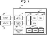
- FIG. 1 is a configuration diagram of an electronic control device 101 according to a first embodiment of the present invention.
- the electronic control device 101 is connected to a sensor 102 and an actuator 103.
- the electronic control device 101 performs a control operation with information obtained from the sensor 102 as an input and outputs a control signal to the actuator 103.
- the actuator 103 is, for example, a brushless DC motor, and the sensor 102 is, for example, a Hall element.
- the electronic control device 101 includes a microcomputer 110, an input circuit 111, an output circuit 112, and a power supply circuit 113.
- the input circuit 111 receives a detection signal from the sensor 102 and gives the detection signal over to the microcomputer 110.
- the output circuit 112 outputs a control signal from the microcomputer 110 to the actuator 103.
- the power supply circuit 113 controls electric power used by the electronic control device 101.
- the microcomputer 110 includes three processor cores (PCs) 121 through 123, an IO 130, a random access memory (RAM) 140, a read only memory (ROM) 150, and a nonvolatile memory 160. These elements are connected by a bus.
- PCs processor cores
- RAM random access memory
- ROM read only memory
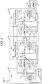
- FIG. 2 is a diagram illustrating processing and data flow among the processor cores 121 through 123.
- Each of functional units described below that are provided in the processor cores 121 through 123 can be implemented as a program module.
- Each processor core reads programs from the ROM 150 and executes these programs, using the RAM 140 as a temporary storage.
- Shared memories 201 through 203 can be configured as storage areas on the RAM 140, which are shared and accessed by each processor core, for example. Initial value of each flag stored in the shared memories 201 through 203 is "invalid".
- the processor core 121 includes a first control unit 210, a first notification unit 211, a first monitoring unit 214, and a first abnormality processing unit 215.
- the first control unit 210 performs a control operation at normal time.
- the first notification unit 211 notifies the processor core 122 that control processing of the first control unit 210 has been completed.
- the first monitoring unit 214 monitors whether control processing of a third control unit 230 (described below) has been completed.
- the first abnormality processing unit 215 performs abnormality processing.
- the processor core 122 includes a second control unit 220, a second notification unit 221, a second notified unit 222, a second confirmation unit 223, a second monitoring unit 224, and a second abnormality processing unit 225.
- the second control unit 220 performs a control operation at normal time.
- the second notification unit 221 notifies the processor core 123 that control processing of the second control unit 220 has been completed.
- the second notified unit 222 receives a notification of completion of the control processing from the first control unit 210.
- the second confirmation unit 223 confirms whether the control processing of the first control unit 210 has been completed and whether the processor core 121 has output an error.
- the second monitoring unit 224 monitors whether the control processing of the first control unit 210 has been completed within a predetermined period.
- the second abnormality processing unit 225 performs abnormality processing.
- the processor core 123 includes a third control unit 230, a third notified unit 232, a third confirmation unit 233, a third monitoring unit 234, and a third abnormality processing unit 235.
- the third control unit 230 performs a control operation at normal time.
- the third notified unit 232 receives a notification of completion of control processing from the second control unit 220.
- the third confirmation unit 233 confirms whether the control processing of the second control unit 220 has been completed and whether the processor core 122 has output an error.
- the third monitoring unit 234 monitors whether the control processing of the second control unit 220 has been completed within a predetermined period.
- the third abnormality processing unit 235 performs abnormality processing.
- the processor core 121 cyclically activates the first control unit 210 according to a timer provided in the processor core 121.
- the first control unit 210 performs the control operation using the signal received from the sensor 102, and outputs a result of the operation to the shared memory 201 as first data.
- the first control unit 210 activates the first notification unit 211.
- the first notification unit 211 writes a value indicating "valid" in a first completion flag on the shared memory 201, and notifies the second notified unit 222 of completion of the control processing.
- a synchronization mechanism such as a spin lock or a semaphore, or an interrupt. This also similarly applies to other notification units to be described below.
- the second confirmation unit 223 reads the first completion flag.
- the first completion flag is "valid" (that is, the control processing of the first control unit 210 has been completed)
- the first data is given over to the second control unit 220 and the second control unit 220 is activated.
- the second confirmation unit 223 rewrites the value with "invalid".
- the second control unit 220 performs the control processing with the first data as an input, and outputs a result of the processing to the shared memory 202 as second data.
- the second control unit 220 activates the second notification unit 221.
- the second notification unit 221 writes a value indicating "valid" in a second completion flag on the shared memory 202, and notifies the third notified unit 232 of completion of the control processing.
- the third notified unit 232 activates the third confirmation unit 233 together with data indicating that the activation source is the third notified unit 232.
- the third confirmation unit 233 reads the second completion flag. In a case where the second completion flag is "valid”, the second data is given over to the third control unit 230, and the third control unit 230 is activated. Immediately after reading the second completion flag, the third confirmation unit 233 rewrites the value with "invalid".
- the third control unit 230 performs the control processing with the second data as an input, and outputs a control signal obtained as a result to the actuator 103.
- the third control unit 230 rewrites a third completion flag on the shared memory 203 with "valid".
- the first control unit 210 In a case where the first control unit 210 has detected abnormality such as the signal from the sensor 102 being out of range, the first control unit 210 rewrites a first error flag on the shared memory 201 with "valid".
- the processor core 122 cyclically activates the second monitoring unit 224.
- An activation cycle of the second monitoring unit 224 is set, for example, in accordance with a cycle in which the first control unit 210 is assumed to complete the processing.
- the second monitoring unit 224 activates the second confirmation unit 223 together with data indicating that the activation source is the second monitoring unit 224.
- the second confirmation unit 223 activates the second abnormality processing unit 225 in a case where the first completion flag is "invalid" (that is, the control processing of the first control unit 210 is incomplete) or the first error flag is "valid".
- the second abnormality processing unit 225 rewrites a second error flag on the shared memory 202 with "valid". Immediately after reading the first error flag, the second confirmation unit 223 rewrites the value with "invalid".
- the processor core 123 cyclically activates the third monitoring unit 234.
- An activation cycle of the third monitoring unit 234 is set, for example, in accordance with a cycle in which the second control unit 220 is assumed to complete the processing.
- the third monitoring unit 234 activates the third confirmation unit 233 together with data indicating that the activation source is the third monitoring unit 234.
- the third confirmation unit 233 activates the third abnormality processing unit 235 in a case where the second completion flag is "invalid" (that is, the control processing of the second control unit 220 is incomplete) or the second error flag is "valid".
- the third confirmation unit 233 rewrites the value with "invalid".
- the third abnormality processing unit 235 After recording information indicating that the third abnormality processing unit 235 has detected abnormality to the nonvolatile memory 160, the third abnormality processing unit 235 stops the actuator 103 and then shuts down the processor core 123. After recordings information indicating that the second abnormality processing unit 225 has detected abnormality to the nonvolatile memory 160, the second abnormality processing unit 225 waits for a fixed time and then shuts down the processor core 122.
- the third monitoring unit 234 activates the second monitoring unit 224 before activating the third confirmation unit 233.
- the third monitoring unit 234 waits for a fixed time to wait for completion of the processing of the second confirmation unit 223, and then reads the second completion flag and the second error flag via the third confirmation unit 233. Since processing of the second confirmation unit 223 is merely reading each flag, the standby time of the third monitoring unit 234 is short.
- the second confirmation unit 223 may notify the third monitoring unit 234 of completion of the processing after completion of the processing, in place of the third monitoring unit 234 waiting for the fixed time. Through these procedures, the second monitoring unit 224 and the third monitoring unit 234 synchronously operate.
- the second monitoring unit 224 operating on the processor core 122 at a preceding stage of the processing is activated from the third monitoring unit 234 operating on the processor core 123 at a subsequent stage of the processing, whereby the abnormality detected by the second confirmation unit 223 is transmitted to the third confirmation unit 233 without separating a large time.
- the second monitoring unit 224 and the third monitoring unit 234 operate without synchronization, there is a possibility of occurrence of a delay in transmission of the abnormality detection between the processor cores 122 and 123 in accordance with a gap in activation timing between the second monitoring unit 224 and the third monitoring unit 234. According to the first embodiment, accumulation of such a propagation delay can be suppressed.
- the processor core 122 activates the second monitoring unit 224 on a cycle T2.
- the processor core 123 activates the third monitoring unit 234 on a cycle T3.
- a timer for activating the second monitoring unit 224, a timer for activating the third monitoring unit 234, and a timer for activating the first control unit 210 are independent of one another.
- T2 and T3 are set to values larger than the activation cycle of the first control unit 210 so that the second monitoring unit 224 and the third monitoring unit 234 do not erroneously detect incompletion of the processing. Further, T3 ⁇ T2 is set as a cycle restriction.
- the second monitoring unit 224 can also monitor incompletion of the processing of the first control unit 210 even in a case where the third monitoring unit 234 is not activated due to abnormality in the timer that activates the third monitoring unit 234, and further, the second monitoring unit 224 is not activated by the third monitoring unit 234.
- the processor core 121 is located at the forefront stage of the control operation but the first monitoring unit 214 is cyclically activated and reads the third completion flag in order to monitor incompletion of the processing of the third control unit 230 of the processor core 123 located at the last stage of the control operation.
- the timer used for this activation is different from the timer that activates the first control unit 210 and the like.
- the first monitoring unit 214 rewrites the value with "invalid”.
- the third completion flag is "invalid”
- the first monitoring unit 214 activates the first abnormality processing unit 215.
- the first abnormality processing unit 215 shuts down the processor core 121. Incompletion of the processing of all the processor cores can be monitored by the first monitoring unit 214.
- the second confirmation unit 223, the third confirmation unit 233, and the first abnormality processing unit 215 may include an error counter.
- the error counter is cleared, and when the first through third completion flags are "invalid", the error counter is incremented by one.
- the error counter exceeds a threshold value, the second abnormality processing unit 225/the third abnormality processing unit 235/the first abnormality processing unit 215 are activated.
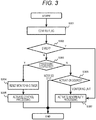
- FIG. 3 is a flowchart for describing the operation of the second confirmation unit 223.
- the third confirmation unit 233 also operates in accordance with a similar flowchart, so that description is omitted.
- each step of FIG. 3 will be described.
- the second confirmation unit 223 reads the first error flag (S301) . In the case where the first error flag is "valid", the processing proceeds to step S307, otherwise proceeds to step S303 (S302).
- the second confirmation unit 223 reads the first completion flag. In the case where the first completion flag is "invalid", the processing proceeds to step S306. Otherwise, the processing proceeds to step S304.
- the second confirmation unit 223 resets the activation timer of the second monitoring unit 224 (S304). For example, when the timer counter is decremented to 0 as time progresses, the timer counter is set to T2 in the case of the timer that activates the second monitoring unit 224.
- the second confirmation unit 223 activates the second control unit 220 (S305).
- the second confirmation unit 223 determines the activation source on the basis of data given at the time of activation (S306). When the activation source is the second monitoring unit 224, the processing proceeds to step S307. When the activation source is the second notified unit 222, the present flowchart is terminated. The second confirmation unit 223 activates the second abnormality processing unit 225 (S307).
- the second control unit 220 is not erroneously activated.
- the activation source is the second notified unit 222 in step S306, abnormality processing different from the processing of the second abnormality processing unit 225 may be performed, such as taking a log of the activation source.
- FIG. 4 is a time chart for describing operation of each unit in a case where a failure occurs in the processor core 121. It is assumed that a failure has occurred in the first control unit 210 at time t1, and the processing does not proceed.
- the third monitoring unit 234 is activated.
- the third monitoring unit 234 activates the second monitoring unit 224.
- the second monitoring unit 224 confirms "invalid" of the first completion flag, and sets the second error flag to "valid”.
- the second monitoring unit 224 activates the second abnormality processing unit 225.
- the third monitoring unit 234 confirms the "valid" of the second error flag, and activates the third abnormality processing unit 235 at the time t6.
- the third monitoring unit 234 waits for a fixed time so as to restart after the time t4.
- the third monitoring unit 234 activates the second monitoring unit 224, whereby the processor core 123 knows the error that has occurred in the processor core 121 at an early stage. As a result, accumulation of delays as the error that has occurred in the processor core 121 is transmitted to the processor core 123 can be suppressed.
- the electronic control device 101 confirms whether each completion flag is "valid" within a predetermined period, thereby to monitor whether each task has been completed within a predetermined period. That is, a deadline monitoring function can be realized.
- FIG. 5 is an example of a software architecture for configuring functions described in the first embodiment.
- a real-time operation system operates on each of the processor cores 121 through 123, and the first control unit 210/the second control unit 220/the third control unit 230, the first monitoring unit 214/the second monitoring unit 224/the third monitoring unit 234, and the second notified unit 222/the third notified unit 232 operate on the real-time OS.
- These programs are registered as OS tasks.
- Execution priorities of the respective tasks are relatively set such that the first control unit 210/the second control unit 220/the third control unit 230 are "medium”, the first monitoring unit 214/the second monitoring unit 224/the third monitoring unit 234 are "high”, and the second notified unit 222/the third notified unit 232 are "low", or the like.
- the first abnormality processing unit 215/the second abnormality processing unit 225/the third abnormality processing unit 235 and the like are also registered as tasks.
- the real-time OS typically has a function to monitor execution time of a task.
- the OS having the execution time monitoring function there are AUTOSAR OS and the like.
- the execution time here is net required execution time excluding time when the task is temporarily stopped out of the time required from the start to completion of the task.
- the real-time OS specifies the task that is the cause of deadline violation from the log stored in a nonvolatile memory 160.
- the first control unit 210/the second control unit 220/the third control unit 230 are monitored for the execution time.
- the cause is in any of the first control unit 210/the second control unit 220/the third control unit 230 or in other processing can be identified.
- the technique described in the first embodiment can detect occurrence of the deadline violation, it is difficult to specify which task is the cause of the violation. Therefore, as in the second embodiment, the task that requires long execution time is identified further using the execution time monitoring function, whereby the task of the cause can be identified when the deadline violation has occurred.
- the present invention is not limited to the above-described embodiments and includes various modifications.
- the above embodiments have been described in detail for describing the present invention in an easy-to-understand manner, and the present invention is not necessarily limited to one including all the described configurations.
- a part of the configuration of a certain embodiment can be replaced with the configuration of another embodiment.
- the configuration of another embodiment can be added to the configuration of a certain embodiment.
- another configuration can be added to, deleted from, replaced with a part of the configurations of each embodiment.
- each of the shared memories 201 through 203 is provided between the processor cores.
- it may be configured such that the processor cores connect in parallel to a single shared memory respectively.
- the processor core 121 may include a first notification unit that receives a notification from another processor core and a first confirmation unit that confirms a log according to the notification. Further, the processor core 123 may include a third notification unit that notifies another processor core of completion of processing.
- a part of the above-described configurations, functions, processing units, and processing means may be realized by hardware by being designed with an integrated circuit or the like. Further, the above-described configurations, functions, and the like may be realized by software in such a manner that the processor interprets and executes programs that realize the respective functions. Information of programs, tables, and files that realize the functions can be stored in a recording device such as a memory, a hard disk, or a solid state drive (SSD), or in a recording medium such as an IC card, an SD card, or a DVD.
- a recording device such as a memory, a hard disk, or a solid state drive (SSD)
- SSD solid state drive
Landscapes
- Engineering & Computer Science (AREA)
- Theoretical Computer Science (AREA)
- Quality & Reliability (AREA)
- Physics & Mathematics (AREA)
- General Engineering & Computer Science (AREA)
- General Physics & Mathematics (AREA)
- Debugging And Monitoring (AREA)
- Microcomputers (AREA)
- Safety Devices In Control Systems (AREA)
Abstract
Description
- The present invention relates to an electronic control device.
- Some electronic control devices such as in-vehicle control devices are configured by a single processor, and some electronic control devices are configured by a multiprocessor for reasons such as a computation amount and troubleshooting. Each processor may include a plurality of processor cores (multicore) for reasons such as suppression of power consumption in response to a request for improvement in processing performance.
-
PTL 1 below describes an electronic control device using a multicore microcomputer. - In
PTL 1, a configuration in which data output by processing of acore 1 is input to acore 2 is adopted, and when thecore 1 has completed the processing, thecore 1 notifies thecore 2 of the completion. InPTL 1, to cope with the case where this notification is wrong, a previous value output by thecore 1 is compared with a latest value placed in a shared memory, and processing of thecore 2 is activated only when a specific condition such as when both the values are different is satisfied. - PTL 1:
JP 2012-108786 A - In an electronic control device in which a next computation device starts processing after completion of processing by another computation device as in the technology described in
PTL 1, it is considered that, when a computation device at a preceding stage outputs an error, a computation device at a subsequent stage executes processing according to the error. At this time, when detection of the error of the computation device at the preceding stage by the computation device at the subsequent stage is delayed, coping with the error by the computation device at the subsequent stage is delayed, and the delay is accumulated in a computation device at a further subsequent stage, and there is a possibility of posing an obstacle to the entire flow. - The present invention has been made in view of the above problems, and an objective is to prevent accumulation of error detection delays that arise in the process of control processing in an electronic control device equipped with a plurality of computation devices.
- An electronic control device according to the present invention includes first through third computation devices. A third computation device monitoring unit activates a second computation device monitoring unit. When the second computation device monitoring unit is activated by the third computation device monitoring unit, the second computation device monitoring unit confirms whether the first computation device has output an error, and notifies the third computation device of a result.
- According to the electronic control device of the present invention, a detection delay when the third computation device detects an error that has occurred in the first computation device can be suppressed.
-
-
FIG. 1 is a configuration diagram of anelectronic control device 101 according to a first embodiment. -
FIG. 2 is a diagram illustrating processing and data flow amongprocessor cores 121 through 123. -
FIG. 3 is a flowchart for describing operation of asecond confirmation unit 223. -
FIG. 4 is a time chart for describing operation of each unit in a case where a failure occurs in theprocessor core 121. -
FIG. 5 is an example of a software architecture for configuring functions described in the first embodiment. -
FIG. 1 is a configuration diagram of anelectronic control device 101 according to a first embodiment of the present invention. Theelectronic control device 101 is connected to asensor 102 and anactuator 103. Theelectronic control device 101 performs a control operation with information obtained from thesensor 102 as an input and outputs a control signal to theactuator 103. Theactuator 103 is, for example, a brushless DC motor, and thesensor 102 is, for example, a Hall element. - The
electronic control device 101 includes amicrocomputer 110, aninput circuit 111, anoutput circuit 112, and apower supply circuit 113. Theinput circuit 111 receives a detection signal from thesensor 102 and gives the detection signal over to themicrocomputer 110. Theoutput circuit 112 outputs a control signal from themicrocomputer 110 to theactuator 103. Thepower supply circuit 113 controls electric power used by theelectronic control device 101. - The
microcomputer 110 includes three processor cores (PCs) 121 through 123, anIO 130, a random access memory (RAM) 140, a read only memory (ROM) 150, and anonvolatile memory 160. These elements are connected by a bus. -
FIG. 2 is a diagram illustrating processing and data flow among theprocessor cores 121 through 123. Each of functional units described below that are provided in theprocessor cores 121 through 123 can be implemented as a program module. Each processor core reads programs from theROM 150 and executes these programs, using theRAM 140 as a temporary storage. Sharedmemories 201 through 203 can be configured as storage areas on theRAM 140, which are shared and accessed by each processor core, for example. Initial value of each flag stored in the sharedmemories 201 through 203 is "invalid". - The
processor core 121 includes afirst control unit 210, afirst notification unit 211, a first monitoring unit 214, and a firstabnormality processing unit 215. Thefirst control unit 210 performs a control operation at normal time. Thefirst notification unit 211 notifies theprocessor core 122 that control processing of thefirst control unit 210 has been completed. The first monitoring unit 214 monitors whether control processing of a third control unit 230 (described below) has been completed. The firstabnormality processing unit 215 performs abnormality processing. - The
processor core 122 includes asecond control unit 220, asecond notification unit 221, a second notifiedunit 222, asecond confirmation unit 223, asecond monitoring unit 224, and a secondabnormality processing unit 225. Thesecond control unit 220 performs a control operation at normal time. Thesecond notification unit 221 notifies theprocessor core 123 that control processing of thesecond control unit 220 has been completed. The second notifiedunit 222 receives a notification of completion of the control processing from thefirst control unit 210. Thesecond confirmation unit 223 confirms whether the control processing of thefirst control unit 210 has been completed and whether theprocessor core 121 has output an error. Thesecond monitoring unit 224 monitors whether the control processing of thefirst control unit 210 has been completed within a predetermined period. The secondabnormality processing unit 225 performs abnormality processing. - The
processor core 123 includes athird control unit 230, a third notifiedunit 232, athird confirmation unit 233, athird monitoring unit 234, and a thirdabnormality processing unit 235. Thethird control unit 230 performs a control operation at normal time. The third notifiedunit 232 receives a notification of completion of control processing from thesecond control unit 220. Thethird confirmation unit 233 confirms whether the control processing of thesecond control unit 220 has been completed and whether theprocessor core 122 has output an error. Thethird monitoring unit 234 monitors whether the control processing of thesecond control unit 220 has been completed within a predetermined period. The thirdabnormality processing unit 235 performs abnormality processing. - The
processor core 121 cyclically activates thefirst control unit 210 according to a timer provided in theprocessor core 121. Thefirst control unit 210 performs the control operation using the signal received from thesensor 102, and outputs a result of the operation to the sharedmemory 201 as first data. When thefirst control unit 210 has completed the control processing, thefirst control unit 210 activates thefirst notification unit 211. - The
first notification unit 211 writes a value indicating "valid" in a first completion flag on the sharedmemory 201, and notifies the second notifiedunit 222 of completion of the control processing. As a method of this notification, a synchronization mechanism such as a spin lock or a semaphore, or an interrupt. This also similarly applies to other notification units to be described below. When the second notifiedunit 222 has received the notification from thefirst notification unit 211, the second notifiedunit 222 activates thesecond confirmation unit 223 together with data indicating that an activation source is the second notifiedunit 222. - The
second confirmation unit 223 reads the first completion flag. In a case where the first completion flag is "valid" (that is, the control processing of thefirst control unit 210 has been completed), the first data is given over to thesecond control unit 220 and thesecond control unit 220 is activated. Immediately after reading the first completion flag, thesecond confirmation unit 223 rewrites the value with "invalid". - The
second control unit 220 performs the control processing with the first data as an input, and outputs a result of the processing to the sharedmemory 202 as second data. When thesecond control unit 220 has completed the control processing, thesecond control unit 220 activates thesecond notification unit 221. - The
second notification unit 221 writes a value indicating "valid" in a second completion flag on the sharedmemory 202, and notifies the third notifiedunit 232 of completion of the control processing. When the third notifiedunit 232 has received the notification from thesecond notification unit 221, the third notifiedunit 232 activates thethird confirmation unit 233 together with data indicating that the activation source is the third notifiedunit 232. - The
third confirmation unit 233 reads the second completion flag. In a case where the second completion flag is "valid", the second data is given over to thethird control unit 230, and thethird control unit 230 is activated. Immediately after reading the second completion flag, thethird confirmation unit 233 rewrites the value with "invalid". - The
third control unit 230 performs the control processing with the second data as an input, and outputs a control signal obtained as a result to theactuator 103. When thethird control unit 230 has completed the control processing, thethird control unit 230 rewrites a third completion flag on the sharedmemory 203 with "valid". - In a case where the
first control unit 210 has detected abnormality such as the signal from thesensor 102 being out of range, thefirst control unit 210 rewrites a first error flag on the sharedmemory 201 with "valid". - The
processor core 122 cyclically activates thesecond monitoring unit 224. An activation cycle of thesecond monitoring unit 224 is set, for example, in accordance with a cycle in which thefirst control unit 210 is assumed to complete the processing. Thesecond monitoring unit 224 activates thesecond confirmation unit 223 together with data indicating that the activation source is thesecond monitoring unit 224. Thesecond confirmation unit 223 activates the secondabnormality processing unit 225 in a case where the first completion flag is "invalid" (that is, the control processing of thefirst control unit 210 is incomplete) or the first error flag is "valid". The secondabnormality processing unit 225 rewrites a second error flag on the sharedmemory 202 with "valid". Immediately after reading the first error flag, thesecond confirmation unit 223 rewrites the value with "invalid". - The
processor core 123 cyclically activates thethird monitoring unit 234. An activation cycle of thethird monitoring unit 234 is set, for example, in accordance with a cycle in which thesecond control unit 220 is assumed to complete the processing. Thethird monitoring unit 234 activates thethird confirmation unit 233 together with data indicating that the activation source is thethird monitoring unit 234. Thethird confirmation unit 233 activates the thirdabnormality processing unit 235 in a case where the second completion flag is "invalid" (that is, the control processing of thesecond control unit 220 is incomplete) or the second error flag is "valid". Immediately after reading the second error flag, thethird confirmation unit 233 rewrites the value with "invalid". - After recording information indicating that the third
abnormality processing unit 235 has detected abnormality to thenonvolatile memory 160, the thirdabnormality processing unit 235 stops theactuator 103 and then shuts down theprocessor core 123. After recordings information indicating that the secondabnormality processing unit 225 has detected abnormality to thenonvolatile memory 160, the secondabnormality processing unit 225 waits for a fixed time and then shuts down theprocessor core 122. - The
third monitoring unit 234 activates thesecond monitoring unit 224 before activating thethird confirmation unit 233. - To execute this activation, for example, an interrupt or the like can be used. After activating the
second monitoring unit 224, thethird monitoring unit 234 waits for a fixed time to wait for completion of the processing of thesecond confirmation unit 223, and then reads the second completion flag and the second error flag via thethird confirmation unit 233. Since processing of thesecond confirmation unit 223 is merely reading each flag, the standby time of thethird monitoring unit 234 is short. Thesecond confirmation unit 223 may notify thethird monitoring unit 234 of completion of the processing after completion of the processing, in place of thethird monitoring unit 234 waiting for the fixed time. Through these procedures, thesecond monitoring unit 224 and thethird monitoring unit 234 synchronously operate. - In this way, the
second monitoring unit 224 operating on theprocessor core 122 at a preceding stage of the processing is activated from thethird monitoring unit 234 operating on theprocessor core 123 at a subsequent stage of the processing, whereby the abnormality detected by thesecond confirmation unit 223 is transmitted to thethird confirmation unit 233 without separating a large time. In contrast, if thesecond monitoring unit 224 and thethird monitoring unit 234 operate without synchronization, there is a possibility of occurrence of a delay in transmission of the abnormality detection between theprocessor cores second monitoring unit 224 and thethird monitoring unit 234. According to the first embodiment, accumulation of such a propagation delay can be suppressed. - The
processor core 122 activates thesecond monitoring unit 224 on a cycle T2. Theprocessor core 123 activates thethird monitoring unit 234 on a cycle T3. A timer for activating thesecond monitoring unit 224, a timer for activating thethird monitoring unit 234, and a timer for activating thefirst control unit 210 are independent of one another. T2 and T3 are set to values larger than the activation cycle of thefirst control unit 210 so that thesecond monitoring unit 224 and thethird monitoring unit 234 do not erroneously detect incompletion of the processing. Further, T3 ≦ T2 is set as a cycle restriction. With the restriction, not only does thesecond monitoring unit 224 operate in synchronization with thethird monitoring unit 234, thesecond monitoring unit 224 can also monitor incompletion of the processing of thefirst control unit 210 even in a case where thethird monitoring unit 234 is not activated due to abnormality in the timer that activates thethird monitoring unit 234, and further, thesecond monitoring unit 224 is not activated by thethird monitoring unit 234. - The
processor core 121 is located at the forefront stage of the control operation but the first monitoring unit 214 is cyclically activated and reads the third completion flag in order to monitor incompletion of the processing of thethird control unit 230 of theprocessor core 123 located at the last stage of the control operation. The timer used for this activation is different from the timer that activates thefirst control unit 210 and the like. Immediately after reading the third completion flag, the first monitoring unit 214 rewrites the value with "invalid". When the third completion flag is "invalid", the first monitoring unit 214 activates the firstabnormality processing unit 215. The firstabnormality processing unit 215 shuts down theprocessor core 121. Incompletion of the processing of all the processor cores can be monitored by the first monitoring unit 214. - The
second confirmation unit 223, thethird confirmation unit 233, and the firstabnormality processing unit 215 may include an error counter. In this case, when the first through third completion flags are "valid", the error counter is cleared, and when the first through third completion flags are "invalid", the error counter is incremented by one. When the error counter exceeds a threshold value, the secondabnormality processing unit 225/the thirdabnormality processing unit 235/the firstabnormality processing unit 215 are activated. -
FIG. 3 is a flowchart for describing the operation of thesecond confirmation unit 223. Thethird confirmation unit 233 also operates in accordance with a similar flowchart, so that description is omitted. Hereinafter, each step ofFIG. 3 will be described. - The
second confirmation unit 223 reads the first error flag (S301) . In the case where the first error flag is "valid", the processing proceeds to step S307, otherwise proceeds to step S303 (S302). - The
second confirmation unit 223 reads the first completion flag. In the case where the first completion flag is "invalid", the processing proceeds to step S306. Otherwise, the processing proceeds to step S304. - The
second confirmation unit 223 resets the activation timer of the second monitoring unit 224 (S304). For example, when the timer counter is decremented to 0 as time progresses, the timer counter is set to T2 in the case of the timer that activates thesecond monitoring unit 224. Thesecond confirmation unit 223 activates the second control unit 220 (S305). - The
second confirmation unit 223 determines the activation source on the basis of data given at the time of activation (S306). When the activation source is thesecond monitoring unit 224, the processing proceeds to step S307. When the activation source is the second notifiedunit 222, the present flowchart is terminated. Thesecond confirmation unit 223 activates the second abnormality processing unit 225 (S307). - According to these steps, in the case where the processing completion of the
first control unit 210 is erroneously notified to the second notifiedunit 222, thesecond control unit 220 is not erroneously activated. In the case where the activation source is the second notifiedunit 222 in step S306, abnormality processing different from the processing of the secondabnormality processing unit 225 may be performed, such as taking a log of the activation source. -
FIG. 4 is a time chart for describing operation of each unit in a case where a failure occurs in theprocessor core 121. It is assumed that a failure has occurred in thefirst control unit 210 at time t1, and the processing does not proceed. At time t2, thethird monitoring unit 234 is activated. At time t3, thethird monitoring unit 234 activates thesecond monitoring unit 224. By time t4, thesecond monitoring unit 224 confirms "invalid" of the first completion flag, and sets the second error flag to "valid". At time t5, thesecond monitoring unit 224 activates the secondabnormality processing unit 225. By time t6, thethird monitoring unit 234 confirms the "valid" of the second error flag, and activates the thirdabnormality processing unit 235 at the time t6. After activating thesecond monitoring unit 224, thethird monitoring unit 234 waits for a fixed time so as to restart after the time t4. - In the
electronic control device 101 according to the first embodiment, thethird monitoring unit 234 activates thesecond monitoring unit 224, whereby theprocessor core 123 knows the error that has occurred in theprocessor core 121 at an early stage. As a result, accumulation of delays as the error that has occurred in theprocessor core 121 is transmitted to theprocessor core 123 can be suppressed. - The
electronic control device 101 according to the first embodiment confirms whether each completion flag is "valid" within a predetermined period, thereby to monitor whether each task has been completed within a predetermined period. That is, a deadline monitoring function can be realized. -
FIG. 5 is an example of a software architecture for configuring functions described in the first embodiment. A real-time operation system (OS) operates on each of theprocessor cores 121 through 123, and thefirst control unit 210/thesecond control unit 220/thethird control unit 230, the first monitoring unit 214/thesecond monitoring unit 224/thethird monitoring unit 234, and the second notifiedunit 222/the third notifiedunit 232 operate on the real-time OS. These programs are registered as OS tasks. Execution priorities of the respective tasks are relatively set such that thefirst control unit 210/thesecond control unit 220/thethird control unit 230 are "medium", the first monitoring unit 214/thesecond monitoring unit 224/thethird monitoring unit 234 are "high", and the second notifiedunit 222/the third notifiedunit 232 are "low", or the like. - Though not illustrated, the first
abnormality processing unit 215/the secondabnormality processing unit 225/the thirdabnormality processing unit 235 and the like are also registered as tasks. - The real-time OS typically has a function to monitor execution time of a task. As the OS having the execution time monitoring function, there are AUTOSAR OS and the like. The execution time here is net required execution time excluding time when the task is temporarily stopped out of the time required from the start to completion of the task. In execution time monitoring processing, the real-time OS specifies the task that is the cause of deadline violation from the log stored in a
nonvolatile memory 160. For example, thefirst control unit 210/thesecond control unit 220/thethird control unit 230 are monitored for the execution time. As a result, when there is deadline violation, whether the cause is in any of thefirst control unit 210/thesecond control unit 220/thethird control unit 230 or in other processing can be identified. - Although the technique described in the first embodiment can detect occurrence of the deadline violation, it is difficult to specify which task is the cause of the violation. Therefore, as in the second embodiment, the task that requires long execution time is identified further using the execution time monitoring function, whereby the task of the cause can be identified when the deadline violation has occurred.
- The present invention is not limited to the above-described embodiments and includes various modifications. For example, the above embodiments have been described in detail for describing the present invention in an easy-to-understand manner, and the present invention is not necessarily limited to one including all the described configurations. Further, a part of the configuration of a certain embodiment can be replaced with the configuration of another embodiment. Further, the configuration of another embodiment can be added to the configuration of a certain embodiment. Further, another configuration can be added to, deleted from, replaced with a part of the configurations of each embodiment.
- In the above embodiments, the configuration in which the error flags and the completion flags are monitored among the processor cores has been described. However, a similar technique can be used in a configuration for monitoring error flags and completion flags among processors in a multiprocessor system.
- In the above embodiments, each of the shared
memories 201 through 203 is provided between the processor cores. However, it may be configured such that the processor cores connect in parallel to a single shared memory respectively. - In the above embodiments, the
processor core 121 may include a first notification unit that receives a notification from another processor core and a first confirmation unit that confirms a log according to the notification. Further, theprocessor core 123 may include a third notification unit that notifies another processor core of completion of processing. - In the above embodiment, the configuration including the three
processor cores 121 through 123 has been described. However, even in a configuration including four or more processor cores, an error at a preceding stage can be notified to a subsequent stage early, adopting a similar technique. - A part of the above-described configurations, functions, processing units, and processing means may be realized by hardware by being designed with an integrated circuit or the like. Further, the above-described configurations, functions, and the like may be realized by software in such a manner that the processor interprets and executes programs that realize the respective functions. Information of programs, tables, and files that realize the functions can be stored in a recording device such as a memory, a hard disk, or a solid state drive (SSD), or in a recording medium such as an IC card, an SD card, or a DVD.
-
- 101
- electronic control device
- 121
- through 123 processor core
- 210
- first control unit
- 211
- first notification unit
- 214
- first monitoring unit
- 215
- first abnormality processing unit
- 220
- second control unit
- 221
- second notification unit
- 222
- second notified unit
- 223
- second confirmation unit
- 224
- second monitoring unit
- 225
- second abnormality processing unit
- 230
- third control unit
- 232
- third notified unit
- 233
- third confirmation unit
- 234
- third monitoring unit
- 235
- third abnormality processing unit
Claims (8)
- An electronic control device for controlling an object to be controlled, the electronic control device comprising:a first computation device, a second computation device, and a third computation device configured to execute processing of controlling the object to be controlled, whereinthe first computation device notifies the second computation device of whether a control operation executed by the first computation device has normally ended,the second computation device includes a second computation device monitoring unit that monitors whether the first computation device has output an error,the third computation device includes a third computation device monitoring unit that monitors whether the second computation device has output an error,the third computation device monitoring unit activates the second computation device monitoring unit before confirming whether the second computation device has output an error, andwhen the second computation device monitoring unit is activated by the third computation device monitoring unit, the second computation device monitoring unit confirms whether the first computation device has output an error and notifies the third computation device of a result of the confirmation.
- The electronic control device according to claim 1, wherein
the third computation device monitoring unit operates on a shorter cycle than the second computation device monitoring unit. - The electronic control device according to claim 2, wherein
the second computation device monitoring unit and the third computation device monitoring unit operate according to timers independent of each other, and
when the second computation device monitoring unit is activated by the third computation device monitoring unit, the second computation device monitoring unit resets the timer that the second computation device monitoring unit relies on. - The electronic control device according to claim 1, wherein
the second computation device monitoring unit monitors whether the first computation device has completed the control operation,
the second computation device starts a control operation when the second computation device monitoring unit has confirmed that the first computation device has completed the control operation,
the third computation device monitoring unit monitors whether the second computation device has completed the control operation, and
the third computation device starts a control operation when the third computation device monitoring unit has confirmed that the second computation device has completed the control operation. - The electronic control device according to claim 4, wherein
the second computation device starts the control operation, using a result of the control operation executed by the first computation device, and
the third computation device starts the control operation, using a result of the control operation executed by the second computation device. - The electronic control device according to claim 4, wherein,
when the second computation device monitoring unit has confirmed that the first computation device has not completed the control operation within a predetermined time, the second computation device outputs an error of the incompletion of the control operation, and
when the third computation device monitoring unit has confirmed that the second computation device has not completed the control operation within a predetermined time, the third computation device outputs an error of the incompletion of the control operation. - The electronic control device according to claim 6, wherein
the electronic control device executes an operating system for controlling operation of the electronic control device, and
the electronic control device monitors a net execution time required to complete the control operations respectively executed by the first computation device, the second computation device, and the third computation device, via the operating system. - The electronic control device according to claim 1, wherein
the first computation device includes a first computation device monitoring unit that monitors whether another computation device has completed a control operation within a predetermined time, and
when the first computation device monitoring unit has confirmed that the another computation device has not completed the control operation within a predetermined time, the first computation device outputs an error of the incompletion of the control operation.
Applications Claiming Priority (2)
| Application Number | Priority Date | Filing Date | Title |
|---|---|---|---|
| JP2016130393A JP6765874B2 (en) | 2016-06-30 | 2016-06-30 | Electronic control device |
| PCT/JP2017/022453 WO2018003560A1 (en) | 2016-06-30 | 2017-06-19 | Electronic control device |
Publications (3)
| Publication Number | Publication Date |
|---|---|
| EP3480700A1 true EP3480700A1 (en) | 2019-05-08 |
| EP3480700A4 EP3480700A4 (en) | 2020-02-26 |
| EP3480700B1 EP3480700B1 (en) | 2022-02-09 |
Family
ID=60786657
Family Applications (1)
| Application Number | Title | Priority Date | Filing Date |
|---|---|---|---|
| EP17819920.4A Not-in-force EP3480700B1 (en) | 2016-06-30 | 2017-06-19 | Electronic control device |
Country Status (3)
| Country | Link |
|---|---|
| EP (1) | EP3480700B1 (en) |
| JP (1) | JP6765874B2 (en) |
| WO (1) | WO2018003560A1 (en) |
Cited By (3)
| Publication number | Priority date | Publication date | Assignee | Title |
|---|---|---|---|---|
| WO2023212119A1 (en) * | 2022-04-26 | 2023-11-02 | Motional Ad Llc | Autonomous vehicle monitoring system using system-on-chip on-die resources |
| WO2025075232A1 (en) * | 2023-10-05 | 2025-04-10 | 주식회사 시옷 | Method and system for recovering from operation errors |
| US12619566B2 (en) | 2022-04-26 | 2026-05-05 | Motional Ad Llc | Scalable configurable chip architecture |
Family Cites Families (6)
| Publication number | Priority date | Publication date | Assignee | Title |
|---|---|---|---|---|
| JPH07262148A (en) * | 1994-03-22 | 1995-10-13 | Nec Corp | Computer system |
| DE19511842A1 (en) * | 1995-03-31 | 1996-10-02 | Teves Gmbh Alfred | Method and circuit arrangement for monitoring a data processing circuit |
| JP4408921B2 (en) * | 2007-08-22 | 2010-02-03 | 株式会社デンソー | Electronics |
| JP2012108786A (en) | 2010-11-18 | 2012-06-07 | Toyota Motor Corp | Microcomputer and processing synchronization method |
| JP2013095379A (en) * | 2011-11-04 | 2013-05-20 | Denso Corp | Vehicle behavior control device |
| DE102012205445A1 (en) * | 2012-04-03 | 2013-10-10 | Siemens Aktiengesellschaft | automation equipment |
-
2016
- 2016-06-30 JP JP2016130393A patent/JP6765874B2/en not_active Expired - Fee Related
-
2017
- 2017-06-19 WO PCT/JP2017/022453 patent/WO2018003560A1/en not_active Ceased
- 2017-06-19 EP EP17819920.4A patent/EP3480700B1/en not_active Not-in-force
Cited By (3)
| Publication number | Priority date | Publication date | Assignee | Title |
|---|---|---|---|---|
| WO2023212119A1 (en) * | 2022-04-26 | 2023-11-02 | Motional Ad Llc | Autonomous vehicle monitoring system using system-on-chip on-die resources |
| US12619566B2 (en) | 2022-04-26 | 2026-05-05 | Motional Ad Llc | Scalable configurable chip architecture |
| WO2025075232A1 (en) * | 2023-10-05 | 2025-04-10 | 주식회사 시옷 | Method and system for recovering from operation errors |
Also Published As
| Publication number | Publication date |
|---|---|
| JP2018005490A (en) | 2018-01-11 |
| EP3480700B1 (en) | 2022-02-09 |
| EP3480700A4 (en) | 2020-02-26 |
| JP6765874B2 (en) | 2020-10-07 |
| WO2018003560A1 (en) | 2018-01-04 |
Similar Documents
| Publication | Publication Date | Title |
|---|---|---|
| CN101149636B (en) | Repositioning system and method | |
| US10585755B2 (en) | Electronic apparatus and method for restarting a central processing unit (CPU) in response to detecting an abnormality | |
| JP2010277303A (en) | Semiconductor device and abnormality detection method | |
| US10102045B2 (en) | Control device, control method and program | |
| EP3480700B1 (en) | Electronic control device | |
| CN106776054A (en) | A deadlock detection method, device and circuit | |
| JP4393954B2 (en) | Microcomputer | |
| JP2007323631A (en) | CPU runaway determination circuit | |
| JP2015014962A (en) | Arithmetic apparatus, arithmetic method, and program | |
| CN1877471B (en) | Task management device and method for control device | |
| JP7012915B2 (en) | controller | |
| CN115904793B (en) | Memory transfer method, system and chip based on multi-core heterogeneous system | |
| US20180089012A1 (en) | Information processing apparatus for analyzing hardware failure | |
| JP4876093B2 (en) | Control device task management device and control device task management method | |
| CN114637631B (en) | A method, apparatus, vehicle, and storage medium for restarting a scheduling table. | |
| CN110832459B (en) | vehicle control device | |
| JPH11175108A (en) | Redundant computer equipment | |
| JP5299681B2 (en) | Program inspection method | |
| JP3724034B2 (en) | Control circuit for production equipment | |
| JP2007011639A (en) | INPUT / OUTPUT CONTROL DEVICE, INFORMATION CONTROL DEVICE, INPUT / OUTPUT CONTROL METHOD, AND INFORMATION CONTROL METHOD | |
| JP2002287856A (en) | Processor-mounted device and delay reset signal generation method | |
| JP2009205276A (en) | Watchdog timer control device, watchdog timer control method, program, and cpu system | |
| CA2619742C (en) | An input/output control apparatus for performing high reliability computations | |
| JP6906369B2 (en) | Computer systems, their control methods, and programs | |
| JPS632922Y2 (en) |
Legal Events
| Date | Code | Title | Description |
|---|---|---|---|
| STAA | Information on the status of an ep patent application or granted ep patent |
Free format text: STATUS: THE INTERNATIONAL PUBLICATION HAS BEEN MADE |
|
| PUAI | Public reference made under article 153(3) epc to a published international application that has entered the european phase |
Free format text: ORIGINAL CODE: 0009012 |
|
| STAA | Information on the status of an ep patent application or granted ep patent |
Free format text: STATUS: REQUEST FOR EXAMINATION WAS MADE |
|
| 17P | Request for examination filed |
Effective date: 20181119 |
|
| AK | Designated contracting states |
Kind code of ref document: A1 Designated state(s): AL AT BE BG CH CY CZ DE DK EE ES FI FR GB GR HR HU IE IS IT LI LT LU LV MC MK MT NL NO PL PT RO RS SE SI SK SM TR |
|
| AX | Request for extension of the european patent |
Extension state: BA ME |
|
| DAV | Request for validation of the european patent (deleted) | ||
| DAX | Request for extension of the european patent (deleted) | ||
| A4 | Supplementary search report drawn up and despatched |
Effective date: 20200127 |
|
| RIC1 | Information provided on ipc code assigned before grant |
Ipc: G06F 11/07 20060101ALI20200121BHEP Ipc: G06F 11/30 20060101AFI20200121BHEP |
|
| RAP3 | Party data changed (applicant data changed or rights of an application transferred) |
Owner name: HITACHI ASTEMO, LTD. |
|
| GRAP | Despatch of communication of intention to grant a patent |
Free format text: ORIGINAL CODE: EPIDOSNIGR1 |
|
| STAA | Information on the status of an ep patent application or granted ep patent |
Free format text: STATUS: GRANT OF PATENT IS INTENDED |
|
| INTG | Intention to grant announced |
Effective date: 20211116 |
|
| GRAS | Grant fee paid |
Free format text: ORIGINAL CODE: EPIDOSNIGR3 |
|
| GRAA | (expected) grant |
Free format text: ORIGINAL CODE: 0009210 |
|
| STAA | Information on the status of an ep patent application or granted ep patent |
Free format text: STATUS: THE PATENT HAS BEEN GRANTED |
|
| AK | Designated contracting states |
Kind code of ref document: B1 Designated state(s): AL AT BE BG CH CY CZ DE DK EE ES FI FR GB GR HR HU IE IS IT LI LT LU LV MC MK MT NL NO PL PT RO RS SE SI SK SM TR |
|
| REG | Reference to a national code |
Ref country code: GB Ref legal event code: FG4D |
|
| REG | Reference to a national code |
Ref country code: CH Ref legal event code: EP Ref country code: AT Ref legal event code: REF Ref document number: 1467945 Country of ref document: AT Kind code of ref document: T Effective date: 20220215 |
|
| REG | Reference to a national code |
Ref country code: DE Ref legal event code: R096 Ref document number: 602017053228 Country of ref document: DE |
|
| REG | Reference to a national code |
Ref country code: IE Ref legal event code: FG4D |
|
| REG | Reference to a national code |
Ref country code: LT Ref legal event code: MG9D |
|
| REG | Reference to a national code |
Ref country code: NL Ref legal event code: MP Effective date: 20220209 |
|
| REG | Reference to a national code |
Ref country code: AT Ref legal event code: MK05 Ref document number: 1467945 Country of ref document: AT Kind code of ref document: T Effective date: 20220209 |
|
| PG25 | Lapsed in a contracting state [announced via postgrant information from national office to epo] |
Ref country code: SE Free format text: LAPSE BECAUSE OF FAILURE TO SUBMIT A TRANSLATION OF THE DESCRIPTION OR TO PAY THE FEE WITHIN THE PRESCRIBED TIME-LIMIT Effective date: 20220209 Ref country code: RS Free format text: LAPSE BECAUSE OF FAILURE TO SUBMIT A TRANSLATION OF THE DESCRIPTION OR TO PAY THE FEE WITHIN THE PRESCRIBED TIME-LIMIT Effective date: 20220209 Ref country code: PT Free format text: LAPSE BECAUSE OF FAILURE TO SUBMIT A TRANSLATION OF THE DESCRIPTION OR TO PAY THE FEE WITHIN THE PRESCRIBED TIME-LIMIT Effective date: 20220609 Ref country code: NO Free format text: LAPSE BECAUSE OF FAILURE TO SUBMIT A TRANSLATION OF THE DESCRIPTION OR TO PAY THE FEE WITHIN THE PRESCRIBED TIME-LIMIT Effective date: 20220509 Ref country code: NL Free format text: LAPSE BECAUSE OF FAILURE TO SUBMIT A TRANSLATION OF THE DESCRIPTION OR TO PAY THE FEE WITHIN THE PRESCRIBED TIME-LIMIT Effective date: 20220209 Ref country code: LT Free format text: LAPSE BECAUSE OF FAILURE TO SUBMIT A TRANSLATION OF THE DESCRIPTION OR TO PAY THE FEE WITHIN THE PRESCRIBED TIME-LIMIT Effective date: 20220209 Ref country code: HR Free format text: LAPSE BECAUSE OF FAILURE TO SUBMIT A TRANSLATION OF THE DESCRIPTION OR TO PAY THE FEE WITHIN THE PRESCRIBED TIME-LIMIT Effective date: 20220209 Ref country code: ES Free format text: LAPSE BECAUSE OF FAILURE TO SUBMIT A TRANSLATION OF THE DESCRIPTION OR TO PAY THE FEE WITHIN THE PRESCRIBED TIME-LIMIT Effective date: 20220209 Ref country code: BG Free format text: LAPSE BECAUSE OF FAILURE TO SUBMIT A TRANSLATION OF THE DESCRIPTION OR TO PAY THE FEE WITHIN THE PRESCRIBED TIME-LIMIT Effective date: 20220509 |
|
| PG25 | Lapsed in a contracting state [announced via postgrant information from national office to epo] |
Ref country code: PL Free format text: LAPSE BECAUSE OF FAILURE TO SUBMIT A TRANSLATION OF THE DESCRIPTION OR TO PAY THE FEE WITHIN THE PRESCRIBED TIME-LIMIT Effective date: 20220209 Ref country code: LV Free format text: LAPSE BECAUSE OF FAILURE TO SUBMIT A TRANSLATION OF THE DESCRIPTION OR TO PAY THE FEE WITHIN THE PRESCRIBED TIME-LIMIT Effective date: 20220209 Ref country code: GR Free format text: LAPSE BECAUSE OF FAILURE TO SUBMIT A TRANSLATION OF THE DESCRIPTION OR TO PAY THE FEE WITHIN THE PRESCRIBED TIME-LIMIT Effective date: 20220510 Ref country code: FI Free format text: LAPSE BECAUSE OF FAILURE TO SUBMIT A TRANSLATION OF THE DESCRIPTION OR TO PAY THE FEE WITHIN THE PRESCRIBED TIME-LIMIT Effective date: 20220209 Ref country code: AT Free format text: LAPSE BECAUSE OF FAILURE TO SUBMIT A TRANSLATION OF THE DESCRIPTION OR TO PAY THE FEE WITHIN THE PRESCRIBED TIME-LIMIT Effective date: 20220209 |
|
| PG25 | Lapsed in a contracting state [announced via postgrant information from national office to epo] |
Ref country code: IS Free format text: LAPSE BECAUSE OF FAILURE TO SUBMIT A TRANSLATION OF THE DESCRIPTION OR TO PAY THE FEE WITHIN THE PRESCRIBED TIME-LIMIT Effective date: 20220609 |
|
| PG25 | Lapsed in a contracting state [announced via postgrant information from national office to epo] |
Ref country code: SM Free format text: LAPSE BECAUSE OF FAILURE TO SUBMIT A TRANSLATION OF THE DESCRIPTION OR TO PAY THE FEE WITHIN THE PRESCRIBED TIME-LIMIT Effective date: 20220209 Ref country code: SK Free format text: LAPSE BECAUSE OF FAILURE TO SUBMIT A TRANSLATION OF THE DESCRIPTION OR TO PAY THE FEE WITHIN THE PRESCRIBED TIME-LIMIT Effective date: 20220209 Ref country code: RO Free format text: LAPSE BECAUSE OF FAILURE TO SUBMIT A TRANSLATION OF THE DESCRIPTION OR TO PAY THE FEE WITHIN THE PRESCRIBED TIME-LIMIT Effective date: 20220209 Ref country code: EE Free format text: LAPSE BECAUSE OF FAILURE TO SUBMIT A TRANSLATION OF THE DESCRIPTION OR TO PAY THE FEE WITHIN THE PRESCRIBED TIME-LIMIT Effective date: 20220209 Ref country code: DK Free format text: LAPSE BECAUSE OF FAILURE TO SUBMIT A TRANSLATION OF THE DESCRIPTION OR TO PAY THE FEE WITHIN THE PRESCRIBED TIME-LIMIT Effective date: 20220209 Ref country code: CZ Free format text: LAPSE BECAUSE OF FAILURE TO SUBMIT A TRANSLATION OF THE DESCRIPTION OR TO PAY THE FEE WITHIN THE PRESCRIBED TIME-LIMIT Effective date: 20220209 |
|
| REG | Reference to a national code |
Ref country code: DE Ref legal event code: R097 Ref document number: 602017053228 Country of ref document: DE |
|
| PG25 | Lapsed in a contracting state [announced via postgrant information from national office to epo] |
Ref country code: AL Free format text: LAPSE BECAUSE OF FAILURE TO SUBMIT A TRANSLATION OF THE DESCRIPTION OR TO PAY THE FEE WITHIN THE PRESCRIBED TIME-LIMIT Effective date: 20220209 |
|
| PLBE | No opposition filed within time limit |
Free format text: ORIGINAL CODE: 0009261 |
|
| STAA | Information on the status of an ep patent application or granted ep patent |
Free format text: STATUS: NO OPPOSITION FILED WITHIN TIME LIMIT |
|
| 26N | No opposition filed |
Effective date: 20221110 |
|
| PG25 | Lapsed in a contracting state [announced via postgrant information from national office to epo] |
Ref country code: MC Free format text: LAPSE BECAUSE OF FAILURE TO SUBMIT A TRANSLATION OF THE DESCRIPTION OR TO PAY THE FEE WITHIN THE PRESCRIBED TIME-LIMIT Effective date: 20220209 |
|
| REG | Reference to a national code |
Ref country code: CH Ref legal event code: PL |
|
| REG | Reference to a national code |
Ref country code: BE Ref legal event code: MM Effective date: 20220630 |
|
| PG25 | Lapsed in a contracting state [announced via postgrant information from national office to epo] |
Ref country code: SI Free format text: LAPSE BECAUSE OF FAILURE TO SUBMIT A TRANSLATION OF THE DESCRIPTION OR TO PAY THE FEE WITHIN THE PRESCRIBED TIME-LIMIT Effective date: 20220209 |
|
| GBPC | Gb: european patent ceased through non-payment of renewal fee |
Effective date: 20220619 |
|
| PG25 | Lapsed in a contracting state [announced via postgrant information from national office to epo] |
Ref country code: LU Free format text: LAPSE BECAUSE OF NON-PAYMENT OF DUE FEES Effective date: 20220619 Ref country code: LI Free format text: LAPSE BECAUSE OF NON-PAYMENT OF DUE FEES Effective date: 20220630 Ref country code: IE Free format text: LAPSE BECAUSE OF NON-PAYMENT OF DUE FEES Effective date: 20220619 Ref country code: FR Free format text: LAPSE BECAUSE OF NON-PAYMENT OF DUE FEES Effective date: 20220630 Ref country code: CH Free format text: LAPSE BECAUSE OF NON-PAYMENT OF DUE FEES Effective date: 20220630 |
|
| PG25 | Lapsed in a contracting state [announced via postgrant information from national office to epo] |
Ref country code: GB Free format text: LAPSE BECAUSE OF NON-PAYMENT OF DUE FEES Effective date: 20220619 Ref country code: BE Free format text: LAPSE BECAUSE OF NON-PAYMENT OF DUE FEES Effective date: 20220630 |
|
| PG25 | Lapsed in a contracting state [announced via postgrant information from national office to epo] |
Ref country code: IT Free format text: LAPSE BECAUSE OF FAILURE TO SUBMIT A TRANSLATION OF THE DESCRIPTION OR TO PAY THE FEE WITHIN THE PRESCRIBED TIME-LIMIT Effective date: 20220209 |
|
| PG25 | Lapsed in a contracting state [announced via postgrant information from national office to epo] |
Ref country code: HU Free format text: LAPSE BECAUSE OF FAILURE TO SUBMIT A TRANSLATION OF THE DESCRIPTION OR TO PAY THE FEE WITHIN THE PRESCRIBED TIME-LIMIT; INVALID AB INITIO Effective date: 20170619 |
|
| PG25 | Lapsed in a contracting state [announced via postgrant information from national office to epo] |
Ref country code: MK Free format text: LAPSE BECAUSE OF FAILURE TO SUBMIT A TRANSLATION OF THE DESCRIPTION OR TO PAY THE FEE WITHIN THE PRESCRIBED TIME-LIMIT Effective date: 20220209 Ref country code: CY Free format text: LAPSE BECAUSE OF FAILURE TO SUBMIT A TRANSLATION OF THE DESCRIPTION OR TO PAY THE FEE WITHIN THE PRESCRIBED TIME-LIMIT Effective date: 20220209 |
|
| PGFP | Annual fee paid to national office [announced via postgrant information from national office to epo] |
Ref country code: DE Payment date: 20240502 Year of fee payment: 8 |
|
| PG25 | Lapsed in a contracting state [announced via postgrant information from national office to epo] |
Ref country code: MT Free format text: LAPSE BECAUSE OF FAILURE TO SUBMIT A TRANSLATION OF THE DESCRIPTION OR TO PAY THE FEE WITHIN THE PRESCRIBED TIME-LIMIT Effective date: 20220209 |
|
| PG25 | Lapsed in a contracting state [announced via postgrant information from national office to epo] |
Ref country code: TR Free format text: LAPSE BECAUSE OF FAILURE TO SUBMIT A TRANSLATION OF THE DESCRIPTION OR TO PAY THE FEE WITHIN THE PRESCRIBED TIME-LIMIT Effective date: 20220209 |
|
| REG | Reference to a national code |
Ref country code: DE Ref legal event code: R119 Ref document number: 602017053228 Country of ref document: DE |
|
| PG25 | Lapsed in a contracting state [announced via postgrant information from national office to epo] |
Ref country code: DE Free format text: LAPSE BECAUSE OF NON-PAYMENT OF DUE FEES Effective date: 20260101 |