EP3480675A1 - Electronic device - Google Patents
Electronic device Download PDFInfo
- Publication number
- EP3480675A1 EP3480675A1 EP18180835.3A EP18180835A EP3480675A1 EP 3480675 A1 EP3480675 A1 EP 3480675A1 EP 18180835 A EP18180835 A EP 18180835A EP 3480675 A1 EP3480675 A1 EP 3480675A1
- Authority
- EP
- European Patent Office
- Prior art keywords
- display panel
- shape memory
- memory component
- flexible display
- electronic device
- Prior art date
- Legal status (The legal status is an assumption and is not a legal conclusion. Google has not performed a legal analysis and makes no representation as to the accuracy of the status listed.)
- Granted
Links
Images


Classifications
-
- G—PHYSICS
- G06—COMPUTING OR CALCULATING; COUNTING
- G06F—ELECTRIC DIGITAL DATA PROCESSING
- G06F1/00—Details not covered by groups G06F3/00 - G06F13/00 and G06F21/00
- G06F1/16—Constructional details or arrangements
- G06F1/1613—Constructional details or arrangements for portable computers
- G06F1/1633—Constructional details or arrangements of portable computers not specific to the type of enclosures covered by groups G06F1/1615 - G06F1/1626
- G06F1/1637—Details related to the display arrangement, including those related to the mounting of the display in the housing
- G06F1/1652—Details related to the display arrangement, including those related to the mounting of the display in the housing the display being flexible, e.g. mimicking a sheet of paper, or rollable
-
- F—MECHANICAL ENGINEERING; LIGHTING; HEATING; WEAPONS; BLASTING
- F03—MACHINES OR ENGINES FOR LIQUIDS; WIND, SPRING, OR WEIGHT MOTORS; PRODUCING MECHANICAL POWER OR A REACTIVE PROPULSIVE THRUST, NOT OTHERWISE PROVIDED FOR
- F03G—SPRING, WEIGHT, INERTIA OR LIKE MOTORS; MECHANICAL-POWER PRODUCING DEVICES OR MECHANISMS, NOT OTHERWISE PROVIDED FOR OR USING ENERGY SOURCES NOT OTHERWISE PROVIDED FOR
- F03G7/00—Mechanical-power-producing mechanisms, not otherwise provided for or using energy sources not otherwise provided for
- F03G7/06—Mechanical-power-producing mechanisms, not otherwise provided for or using energy sources not otherwise provided for using expansion or contraction of bodies due to heating, cooling, moistening, drying or the like
- F03G7/061—Mechanical-power-producing mechanisms, not otherwise provided for or using energy sources not otherwise provided for using expansion or contraction of bodies due to heating, cooling, moistening, drying or the like characterised by the actuating element
- F03G7/0614—Mechanical-power-producing mechanisms, not otherwise provided for or using energy sources not otherwise provided for using expansion or contraction of bodies due to heating, cooling, moistening, drying or the like characterised by the actuating element using shape memory elements
-
- G—PHYSICS
- G02—OPTICS
- G02F—OPTICAL DEVICES OR ARRANGEMENTS FOR THE CONTROL OF LIGHT BY MODIFICATION OF THE OPTICAL PROPERTIES OF THE MEDIA OF THE ELEMENTS INVOLVED THEREIN; NON-LINEAR OPTICS; FREQUENCY-CHANGING OF LIGHT; OPTICAL LOGIC ELEMENTS; OPTICAL ANALOGUE/DIGITAL CONVERTERS
- G02F1/00—Devices or arrangements for the control of the intensity, colour, phase, polarisation or direction of light arriving from an independent light source, e.g. switching, gating or modulating; Non-linear optics
- G02F1/01—Devices or arrangements for the control of the intensity, colour, phase, polarisation or direction of light arriving from an independent light source, e.g. switching, gating or modulating; Non-linear optics for the control of the intensity, phase, polarisation or colour
- G02F1/13—Devices or arrangements for the control of the intensity, colour, phase, polarisation or direction of light arriving from an independent light source, e.g. switching, gating or modulating; Non-linear optics for the control of the intensity, phase, polarisation or colour based on liquid crystals, e.g. single liquid crystal display cells
- G02F1/133—Constructional arrangements; Operation of liquid crystal cells; Circuit arrangements
- G02F1/1333—Constructional arrangements; Manufacturing methods
- G02F1/133305—Flexible substrates, e.g. plastics, organic film
-
- G—PHYSICS
- G06—COMPUTING OR CALCULATING; COUNTING
- G06F—ELECTRIC DIGITAL DATA PROCESSING
- G06F1/00—Details not covered by groups G06F3/00 - G06F13/00 and G06F21/00
- G06F1/16—Constructional details or arrangements
- G06F1/1613—Constructional details or arrangements for portable computers
- G06F1/1615—Constructional details or arrangements for portable computers with several enclosures having relative motions, each enclosure supporting at least one I/O or computing function
- G06F1/1616—Constructional details or arrangements for portable computers with several enclosures having relative motions, each enclosure supporting at least one I/O or computing function with folding flat displays, e.g. laptop computers or notebooks having a clamshell configuration, with body parts pivoting to an open position around an axis parallel to the plane they define in closed position
-
- G—PHYSICS
- G09—EDUCATION; CRYPTOGRAPHY; DISPLAY; ADVERTISING; SEALS
- G09F—DISPLAYING; ADVERTISING; SIGNS; LABELS OR NAME-PLATES; SEALS
- G09F9/00—Indicating arrangements for variable information in which the information is built-up on a support by selection or combination of individual elements
- G09F9/30—Indicating arrangements for variable information in which the information is built-up on a support by selection or combination of individual elements in which the desired character or characters are formed by combining individual elements
- G09F9/301—Indicating arrangements for variable information in which the information is built-up on a support by selection or combination of individual elements in which the desired character or characters are formed by combining individual elements flexible foldable or roll-able electronic displays, e.g. thin LCD, OLED
-
- G—PHYSICS
- G06—COMPUTING OR CALCULATING; COUNTING
- G06F—ELECTRIC DIGITAL DATA PROCESSING
- G06F1/00—Details not covered by groups G06F3/00 - G06F13/00 and G06F21/00
- G06F1/16—Constructional details or arrangements
- G06F1/20—Cooling means
- G06F1/203—Cooling means for portable computers, e.g. for laptops
-
- G—PHYSICS
- G06—COMPUTING OR CALCULATING; COUNTING
- G06F—ELECTRIC DIGITAL DATA PROCESSING
- G06F2200/00—Indexing scheme relating to G06F1/04 - G06F1/32
- G06F2200/20—Indexing scheme relating to G06F1/20
- G06F2200/203—Heat conductive hinge
Definitions
- the invention is related to an electronic device, and particularly to an electronic device having a flexible display panel.
- the aesthetic quality of the appearance of the notebook computer in the closed state is also reduced.
- the back cover of the upper body of the curved display panel is formed in an arc-shape, which increases the size of the overall notebook computer and makes it inconvenient to carry.
- the invention provides an electronic device having a flexible display panel which is capable of moving between a first position and a second position.
- the flexible display panel is in a flat shape at the first position, which facilitates the upper body and the lower body of the electronic device to be tightly combined when they are closed relative to each other, and the flexible display panel is in a curved shape at the second position to be used as a curved display panel.
- An electronic device provided by the invention includes a flexible display panel and a shape memory component.
- the flexible display panel is driven by the shape memory component, wherein when a temperature of the shape memory component is lower than a default temperature range, the shape memory component is formed as a first shape, so that the flexible display panel is capable of being located at a first position.
- the shape memory component is formed as a second shape, so that the flexible display panel is driven to be moved to a second position.
- the electronic device further includes two supporting elements which are respectively secured on both sides of the flexible display panel and the shape memory component is connected to the supporting elements.
- the electronic device further includes a heat source, and the heat source is thermally coupled to the shape memory component.
- the electronic device further includes a heat-conducting element disposed between the heat source and the shape memory component to transmit the heat generated by the heat source to the shape memory component.
- the electronic device further includes a first housing, a second housing and an elastic element.
- the flexible display panel and the shape memory component are disposed between the first housing and the second housing, and the flexible display panel is connected to the second housing.
- the elastic element is disposed between the first housing and the second housing, and adapted to be deformed when the flexible display panel is moved between the first position and the second position.
- the elastic element is disposed around a position near the edge of the first housing and the second housing.
- the flexible display panel is in a flat shape at the first position, the flexible display panel is in a curved shape at the second position, and a radius of curvature of the flexible display panel at the second position ranges from 3800 mm to 4200 mm.
- the shape memory component is attached to the flexible display panel.
- the default temperature range ranges from 40°C to 65°C.
- the shape memory component includes an iron-based alloy, a nickel-titanium alloy or a copper-based alloy.
- the electronic device of the invention is designed in the manner that the flexible display panel is driven by the shape memory component, and the flexible display panel can be moved between the first position and the second position.
- the electronic device is formed as the first shape; when the temperature of the electronic device is higher than the default temperature, the electronic device is formed as the second shape.
- the flexible display panel can be formed in the flat shape at the first position, which facilitates the upper body and the lower body of the electronic device to be closed tightly so that the appearance of the electronic device is integrated in a closed state, and the overall electronic device has a smaller thickness.
- the shape memory component is subjected to heat and deformed such that the flexible display panel is at the second position, and thus the flexible display panel can be used as a curved display panel.
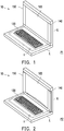
- FIG. 1 is a perspective view illustrating a flexible display panel of an electronic device at a first position according to an embodiment of the invention.
- FIG. 2 is a perspective view illustrating the flexible display panel of the electronic device in FIG. 1 at a second position.
- an electronic device 10 is exemplified as a notebook computer.
- the electronic device 10 may be a tablet PC, a display and the like, which should not be construed as a limitation to the invention.
- the electronic device 10 includes an upper body U and a lower body L, wherein the upper body U is pivoted to the lower body L, and the upper body U may be closed or opened relative to the lower body L.
- the upper body U of the electronic device 10 includes a flexible display panel 100.
- the flexible display panel 100 may be exemplified as a flexible organic light emitting diode panel.
- the flexible display panel 100 may be other types of flexible display panel, and the invention provides no limitation to the type of the flexible display panel.
- the lower body L includes a heat source H and a heat-conducting element thermally coupled to the heat source H.
- the heat source H is, for example, a CPU or a GPU, but the invention provides no limitation to the type of the heat source H.
- the heat-conducting element is exemplified as a heat pipe 130, but the invention provides no limitation to the type of the heat-conducting element.
- the heat pipe 130 may be extended from the heat source H of the lower body L to the upper body U.
- the electronic device 10 enables the flexible display panel 100 in a specific state to be automatically deformed from the flat display panel shown in FIG. 1 to the curved display panel shown in FIG. 2 . Descriptions in this regard are incorporated below.
- FIG. 3 is a schematic view illustrating a portion of component in an upper body of the electronic device in FIG. 1 at the first position.
- FIG. 4 is a schematic view illustrating the component in FIG. 3 deformed to be at the second position. It should be indicated that, in order to clearly describe relative relationship between the flexible display panel 100, the shape memory component 110, the supporting element 120 and a portion of the heat pipe 130 in the upper body U, FIG. 3 and FIG. 4 only schematically illustrate the above-mentioned components. Referring to FIG. 3 and FIG. 4 , in the embodiment, the upper body U of the electronic device 10 is provided with the shape memory component 110 and the two supporting elements 120 therein.
- the two supporting elements 120 are disposed on both ends of the shape memory component 110, and connected to both ends of the flexible display panel 100.
- FIG. 3 shows that the heat pipe 130 extended from the heat source H of the lower body L to the upper body U is located at a position near both ends of the shape memory component 110. It should be indicted that the heat pipe 130 may be extended from the heat source H of the lower body L to a position near the shape memory component 110 on the upper body U. If the upper body U is provided with the heat source H therein, the heat pipe 130 may only be disposed in the upper body U, and extended from the heat source H to the position near the shape memory component 110.
- the configuration of the heat-conducting element 130 in the drawing serves for exemplary purpose only, and the actual circumstances may be adjusted depending on the configuration of the components of the electronic device 10.
- the invention provides no limitation to the overlapping range of the heat-conducting element 130 and the shape memory component 110.
- the heat-conducting element 130 may partially pass through the shape memory component 110.
- the heat-conducting element 130 may completely pass through the shape memory component 110, which should not be construed as a limitation to the invention.
- the invention provides no limitation to the method through which the heat source H transmits the heat to the shape memory component 110.
- the heat source H may transmit heat to the shape memory component 110 by directly contacting the shape memory component 110 without using the heat-conducting element 130, such that the energy consumption caused by transmitting heat energy through a plurality of different media can be reduced.
- the material of the shape memory component 110 is a shape memory alloy (SAM).
- SAM shape memory alloy
- the shape memory alloy changes the shape thereof with the material which can change the metal phase thereof at a specific temperature.
- the shape memory alloy is exhibited in different phases at different temperatures, for example, the shape memory alloy is exhibited in a martersite phase at a relative low temperature, and exhibited in an austenite phase at a relative high temperature.
- the shape memory alloy can be deformed from an initial shape when the temperature is changed and changed back to the initial shape when the temperature is returned to the original temperature. Therefore, in the embodiment, the shape memory component 110 can be deformed spontaneously at different temperatures.
- the material of the shape memory component 110 is, for example, an iron-based alloy, a nickel-titanium alloy or a copper-based alloy. Certainly, the material of the shape memory component 110 is not limited thereto. The designer may select other metal that is exhibited in the martersite phase at room temperature and exhibited in austenite phase at the operating temperature of the heat source H.
- the temperature of the heat source H is relatively low, and the shape memory component 110 is formed as a first shape S1, and the flexible display panel 100 is correspondingly located at a first position P1.
- the temperature of the heat source H is increased, and the heat pipe 130 transmits the heat to a position near the shape memory component 110 such that the shape memory component 110 is deformed from the first shape S1 to a second shape S2.
- the flexible display panel 100 is deformed correspondingly from the first position P1 to a second position P2.
- the flexible display panel 100 and the shape memory component 110 are not directly adhered to each other, and the flexible display panel 100 is driven by the shape memory component 110 through the supporting element 120.
- the flexible display panel 100 may be directly secured to the shape memory component 110 without necessarily being connected to the shape memory component 110 by the supporting element 120.
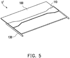
- FIG. 5 is a schematic view illustrating a portion of component in an electronic device according to another embodiment of the invention.
- the shape memory component 110 in an upper body U' may be directly attached to the flexible display panel 100 and directly drives the flexible display panel 100 to change position when the shape memory component 110 is deformed, which can reduce space for disposing the supporting element 120 and the spare space can be used for disposing other component.
- FIG. 6 is a cross-sectional view illustrating an upper body of a flexible display panel at the first position.
- the viewing angle illustrated in FIG. 6 is, for example, line A-A taken along FIG. 3 .
- the upper body U (shown in FIG. 1 ) of the electronic device 10 (shown in FIG. 1 ) is provided with a first housing 140, a second housing 150 and an elastic element E.
- the first housing 140 is a back cover of the electronic device 10
- the second housing 150 is a front frame of the electronic device 10, which should not be construed as a limitation to the invention.
- the flexible display panel 100 and the shape memory component 110 are disposed between the first housing 140 and the second housing 150, and the two supporting elements 120 are connected to the second housing 150.
- the flexible display panel 100 has a display surface and a non-display surface, and the display surface is exposed to the second housing 150.
- the elastic element E is disposed between the first housing 140 and the second housing 150, and for example, disposed around a position near the edge of the first housing 140 and the second housing 150, such that the first housing 140 and the second housing 150 can be moved relatively.
- the material of the elastic element E is a spring; the material of the elastic element E may be rubber or other elastic material.
- the invention provides no limitation to the material of the elastic element E.
- the elastic element E is adapted to be deformed when the flexible display panel 100 is moved between the first position P1 and the second position P2.
- the default temperature range T is a ranged that is exceeded when the electronic device 10 is heated by the heat source H under operation.
- the selected default temperature range T within which the material of the shape memory component 110 is deformed may range from 40° C to 65°C.
- the shape memory component 110 When the temperature of the shape memory component 110 is lower than the default temperature range T, the shape memory component 110 is formed as the first shape S1 such that the flexible display panel 100 is located at the first position P1 and the shape memory component 110 is in the martersite phase, wherein the flexible display panel 100 is exhibited in the flat shape at the first position PI, which reduces the size of the electronic device 10 when the upper body U and the lower body L are closed relative to each other, and makes it more convenient to carry.
- the first housing 140 since the first housing 140 is not exhibited in the arc-shape, no gap is formed when the upper body U and the lower body L are closed relative to each other, such that foreign substance from external environment cannot easily get into the electronic device 10 to cause increase of the possibility of damage to the inner component of the electronic device 10.
- FIG. 7 is a cross-sectional view illustrating an upper body of a flexible display panel at the second position.
- the viewing angle in FIG. 7 is, for example, line B-B taken along FIG. 4 .
- the heat pipe 130 transmits heat to the position near the shape memory component 110 such that the shape memory component 110 is deformed from the first shape S1 to the second shape S2.
- the shape memory component 110 is in the austenite phase.
- the two supporting elements 120 are disposed on both ends of the shape memory component 110 and connected to the both ends of the flexible display panel 100, when the shape memory component 110 is deformed, the relative positions of the two supporting elements 120 are changed as well; accordingly, the flexible display panel 100 is correspondingly deformed from the first position P1 to the second position P2.
- the flexible display panel 100 is in a curved shape at the second position P2, and the radius of curvature of the flexible display panel 100 at the second position P2 ranges from 3800 mm to 4200 mm.
- the range of the radius of curvature of the flexible display panel 100 at the second position P2 is not limited thereto.
- the flexible display panel 100 When the flexible display panel 100 is in the curved state, the flexible display panel 100 has a better visual effect as compared with conventional flat display panel in known technologies; for example, the visible angle is broader, the depth of field is reinforced and the contrast ratio is higher as compared with conventional flat display panel.
- first shape S1 and the second shape S2 are in flat shape and curved shape respectively, the first shape S1 and the second shape S2 may be in any shape within the deformation range of the flexible display panel, and the invention provides no limitation thereto.
- the second housing 150 since the second housing 150 is connected to the two supporting elements 120, the position of the second housing 150 is changed as well such that the elastic element E is deformed. In the embodiment, the second housing 150 is moved relative to the first housing 140 by the elastic element E as shown in FIG. 6 and FIG. 7 .
- the heat generated by the heat source H is waste heat generated by the electronic device 10 under operation.
- it is generally required to dispose a fan or a heat-dissipating fin to transmit the waste heat to the outside of the notebook computer. If the fan or heat-dissipating fin is not provided, the waste heat is accumulated in the notebook computer and causes negative effect on the component in the notebook computer.
- the heat generated by the heat source H is transmitted to the shape memory component 110 to recycle a portion of the waste heat for reuse, so that the shape memory component 110 does not require an additional heat source.
- a portion of the waste heat transmitted to the shape memory component 110 can heat the shape memory component 110 to reach the temperature for phase change, such that the electrical consumption required for adding an additional heat source for heating in conventional technologies can be saved. Since a portion of the waste heat is transmitted to the shape memory component 110 for the purpose of heating, which facilitates the overall electronic device 10 to dissipate the heat. For the electronic device 10, when the sum of waste heat to be discharged is reduced, the required heat-dissipating device can be reduced or cancelled and the spare space can be used for other purpose.
- the electronic device of the invention uses the shape memory component in cooperation with the flexible display panel.
- the temperature of the shape memory component does not exceed the default temperature range
- the flexible display panel of the electronic device is maintained to be in a flat shape so that the upper body and the lower body can be tightly combined when they are closed relative to each other, which reduces the size when the upper body and the lower body are closed relative to each other and makes it more convenient to carry.
- the upper body since it is not required for the upper body to be formed in the arc-shape, the upper body can be tightly closed on the lower body, such that the foreign substance from the outer environment does not easily get into the electronic device to cause damage to the inner component of the electronic device.
- the heat source of the electronic device When the electronic device is in use, the heat source of the electronic device generates heat. At this time, the heat is transmitted to the shape memory component by the heat-conducting element, and the temperature of the shape memory component exceeds the default temperature range to generate phase change; as a result, the shape of the shape memory component is changed so that the flexible display panel is driven to be moved accordingly. Meanwhile, the flexible display panel is in the curved shape so that the user can acquire a better visual effect through the curved display panel than the flat display panel. Moreover, since the heat used by the shape memory component is the waste heat generated by the electronic device, the default temperature range can be reached or exceeded without configuration of an additional heat source for the shape memory component, and the electrical consumption required for adding additional heat source can be saved. Apart from that, since a portion of the waste heat is recycled by the shape memory component for the purpose of deformation, the sum of waste heat in the electronic device is reduced, which facilitates the electronic device to dissipate heat.
Landscapes
- Engineering & Computer Science (AREA)
- Physics & Mathematics (AREA)
- Theoretical Computer Science (AREA)
- Computer Hardware Design (AREA)
- General Physics & Mathematics (AREA)
- General Engineering & Computer Science (AREA)
- Chemical & Material Sciences (AREA)
- Combustion & Propulsion (AREA)
- Human Computer Interaction (AREA)
- Mathematical Physics (AREA)
- Nonlinear Science (AREA)
- Mechanical Engineering (AREA)
- Optics & Photonics (AREA)
- Crystallography & Structural Chemistry (AREA)
- Devices For Indicating Variable Information By Combining Individual Elements (AREA)
Abstract
Description
- The invention is related to an electronic device, and particularly to an electronic device having a flexible display panel.
- In order to meet a variety of users' demands, existing display panels not only include conventional flat display panels but also include curved display panels. However, on the market, curved display is rarely applied to, for example, notebook computer and other portable electronic devices. One of the reasons is that, if the upper body of the notebook computer is provided with a curved display panel, when the upper body of the notebook computer is closed on the lower body, a non-uniformed gap is formed between the curved display panel and the operating surface (i.e., the surface on which the keyboard and the touch panel are located) of the lower body. The gap keeps the upper body of the notebook computer from being tightly combined with the lower body, and foreign substance is likely to get into the notebook computer easily, which increases chance of damage. In addition, the aesthetic quality of the appearance of the notebook computer in the closed state is also reduced. Moreover, the back cover of the upper body of the curved display panel is formed in an arc-shape, which increases the size of the overall notebook computer and makes it inconvenient to carry.
- The invention provides an electronic device having a flexible display panel which is capable of moving between a first position and a second position. The flexible display panel is in a flat shape at the first position, which facilitates the upper body and the lower body of the electronic device to be tightly combined when they are closed relative to each other, and the flexible display panel is in a curved shape at the second position to be used as a curved display panel.
- An electronic device provided by the invention includes a flexible display panel and a shape memory component. The flexible display panel is driven by the shape memory component, wherein when a temperature of the shape memory component is lower than a default temperature range, the shape memory component is formed as a first shape, so that the flexible display panel is capable of being located at a first position. When the temperature of the shape memory component is higher than the default temperature range, the shape memory component is formed as a second shape, so that the flexible display panel is driven to be moved to a second position.
- In an embodiment of the invention, the electronic device further includes two supporting elements which are respectively secured on both sides of the flexible display panel and the shape memory component is connected to the supporting elements.
- In an embodiment of the invention, the electronic device further includes a heat source, and the heat source is thermally coupled to the shape memory component.
- In an embodiment of the invention, the electronic device further includes a heat-conducting element disposed between the heat source and the shape memory component to transmit the heat generated by the heat source to the shape memory component.
- In an embodiment of the invention, the electronic device further includes a first housing, a second housing and an elastic element. The flexible display panel and the shape memory component are disposed between the first housing and the second housing, and the flexible display panel is connected to the second housing. The elastic element is disposed between the first housing and the second housing, and adapted to be deformed when the flexible display panel is moved between the first position and the second position.
- In an embodiment of the invention, the elastic element is disposed around a position near the edge of the first housing and the second housing.
- In an embodiment of the invention, the flexible display panel is in a flat shape at the first position, the flexible display panel is in a curved shape at the second position, and a radius of curvature of the flexible display panel at the second position ranges from 3800 mm to 4200 mm.
- In an embodiment of the invention, the shape memory component is attached to the flexible display panel.
- In an embodiment of the invention, the default temperature range ranges from 40°C to 65°C.
- In an embodiment of the invention, the shape memory component includes an iron-based alloy, a nickel-titanium alloy or a copper-based alloy.
- In summary, the electronic device of the invention is designed in the manner that the flexible display panel is driven by the shape memory component, and the flexible display panel can be moved between the first position and the second position. When the temperature of the electronic device is lower than the default temperature, the electronic device is formed as the first shape; when the temperature of the electronic device is higher than the default temperature, the electronic device is formed as the second shape. If the electronic device is exemplified as the notebook computer, when the electronic device is not in use, the flexible display panel can be formed in the flat shape at the first position, which facilitates the upper body and the lower body of the electronic device to be closed tightly so that the appearance of the electronic device is integrated in a closed state, and the overall electronic device has a smaller thickness. When the electronic device is in use, the shape memory component is subjected to heat and deformed such that the flexible display panel is at the second position, and thus the flexible display panel can be used as a curved display panel.
- In order to make the aforementioned features and advantages of the invention more comprehensible, embodiments accompanying figures are described in detail below.
-
-
FIG. 1 is a perspective view illustrating a flexible display panel of an electronic device at a first position according to an embodiment of the invention. -
FIG. 2 is a perspective view illustrating the flexible display panel of the electronic device inFIG. 1 at a second position. -
FIG. 3 is a schematic view illustrating a portion of component in an upper body of the electronic device inFIG. 1 at the first position. -
FIG. 4 is a schematic view illustrating the component inFIG. 3 deformed to be at the second position. -
FIG. 5 is a schematic view illustrating a portion of component in an electronic device according to another embodiment of the invention. -
FIG. 6 is a cross-sectional view illustrating an upper body of a flexible display panel at the first position. -
FIG. 7 is a cross-sectional view illustrating an upper body of a flexible display panel at the second position. -
FIG. 1 is a perspective view illustrating a flexible display panel of an electronic device at a first position according to an embodiment of the invention.FIG. 2 is a perspective view illustrating the flexible display panel of the electronic device inFIG. 1 at a second position. Referring toFIG. 1 and FIG. 2 , in the embodiment, anelectronic device 10 is exemplified as a notebook computer. Certainly, in other embodiment, theelectronic device 10 may be a tablet PC, a display and the like, which should not be construed as a limitation to the invention. In the embodiment, theelectronic device 10 includes an upper body U and a lower body L, wherein the upper body U is pivoted to the lower body L, and the upper body U may be closed or opened relative to the lower body L. In the embodiment, the upper body U of theelectronic device 10 includes aflexible display panel 100. In the embodiment, theflexible display panel 100 may be exemplified as a flexible organic light emitting diode panel. Certainly, theflexible display panel 100 may be other types of flexible display panel, and the invention provides no limitation to the type of the flexible display panel. - In the embodiment, the lower body L includes a heat source H and a heat-conducting element thermally coupled to the heat source H. In the embodiment, the heat source H is, for example, a CPU or a GPU, but the invention provides no limitation to the type of the heat source H. In addition, in the embodiment, the heat-conducting element is exemplified as a
heat pipe 130, but the invention provides no limitation to the type of the heat-conducting element. Theheat pipe 130 may be extended from the heat source H of the lower body L to the upper body U. In the embodiment, theelectronic device 10 enables theflexible display panel 100 in a specific state to be automatically deformed from the flat display panel shown inFIG. 1 to the curved display panel shown inFIG. 2 . Descriptions in this regard are incorporated below. -
FIG. 3 is a schematic view illustrating a portion of component in an upper body of the electronic device inFIG. 1 at the first position.FIG. 4 is a schematic view illustrating the component inFIG. 3 deformed to be at the second position. It should be indicated that, in order to clearly describe relative relationship between theflexible display panel 100, theshape memory component 110, the supportingelement 120 and a portion of theheat pipe 130 in the upper body U,FIG. 3 and FIG. 4 only schematically illustrate the above-mentioned components. Referring toFIG. 3 and FIG. 4 , in the embodiment, the upper body U of theelectronic device 10 is provided with theshape memory component 110 and the two supportingelements 120 therein. The two supportingelements 120 are disposed on both ends of theshape memory component 110, and connected to both ends of theflexible display panel 100.FIG. 3 shows that theheat pipe 130 extended from the heat source H of the lower body L to the upper body U is located at a position near both ends of theshape memory component 110. It should be indicted that theheat pipe 130 may be extended from the heat source H of the lower body L to a position near theshape memory component 110 on the upper body U. If the upper body U is provided with the heat source H therein, theheat pipe 130 may only be disposed in the upper body U, and extended from the heat source H to the position near theshape memory component 110. - In addition, the configuration of the heat-conducting
element 130 in the drawing serves for exemplary purpose only, and the actual circumstances may be adjusted depending on the configuration of the components of theelectronic device 10. The invention provides no limitation to the overlapping range of the heat-conductingelement 130 and theshape memory component 110. For example, the heat-conductingelement 130 may partially pass through theshape memory component 110. In another example, the heat-conductingelement 130 may completely pass through theshape memory component 110, which should not be construed as a limitation to the invention. However, the invention provides no limitation to the method through which the heat source H transmits the heat to theshape memory component 110. In other embodiment, the heat source H may transmit heat to theshape memory component 110 by directly contacting theshape memory component 110 without using the heat-conductingelement 130, such that the energy consumption caused by transmitting heat energy through a plurality of different media can be reduced. - In the embodiment, the material of the
shape memory component 110 is a shape memory alloy (SAM). The shape memory alloy changes the shape thereof with the material which can change the metal phase thereof at a specific temperature. Furthermore, the shape memory alloy is exhibited in different phases at different temperatures, for example, the shape memory alloy is exhibited in a martersite phase at a relative low temperature, and exhibited in an austenite phase at a relative high temperature. With the characteristic of being exhibited in a different phases at different temperatures, the shape memory alloy can be deformed from an initial shape when the temperature is changed and changed back to the initial shape when the temperature is returned to the original temperature. Therefore, in the embodiment, theshape memory component 110 can be deformed spontaneously at different temperatures. - In the embodiment, the material of the
shape memory component 110 is, for example, an iron-based alloy, a nickel-titanium alloy or a copper-based alloy. Certainly, the material of theshape memory component 110 is not limited thereto. The designer may select other metal that is exhibited in the martersite phase at room temperature and exhibited in austenite phase at the operating temperature of the heat source H. - In the embodiment, as shown in
FIG. 1 andFIG. 3 , when theelectronic device 10 is not in operation, the temperature of the heat source H is relatively low, and theshape memory component 110 is formed as a first shape S1, and theflexible display panel 100 is correspondingly located at a first position P1. As shown inFIG. 2 andFIG. 4 , when theelectronic device 10 is in operation, the temperature of the heat source H is increased, and theheat pipe 130 transmits the heat to a position near theshape memory component 110 such that theshape memory component 110 is deformed from the first shape S1 to a second shape S2. Since the two supportingelements 120 are disposed on both ends of theshape memory component 110 and connected to both ends of theflexible display panel 100, when theshape memory component 110 is deformed, the relative positions of the two supportingelements 120 are also changed; accordingly, theflexible display panel 100 is deformed correspondingly from the first position P1 to a second position P2. In the embodiment, theflexible display panel 100 and theshape memory component 110 are not directly adhered to each other, and theflexible display panel 100 is driven by theshape memory component 110 through the supportingelement 120. Certainly, in other embodiment, theflexible display panel 100 may be directly secured to theshape memory component 110 without necessarily being connected to theshape memory component 110 by the supportingelement 120. -
FIG. 5 is a schematic view illustrating a portion of component in an electronic device according to another embodiment of the invention. Referring toFIG. 5 , in the embodiment, theshape memory component 110 in an upper body U' may be directly attached to theflexible display panel 100 and directly drives theflexible display panel 100 to change position when theshape memory component 110 is deformed, which can reduce space for disposing the supportingelement 120 and the spare space can be used for disposing other component. -
FIG. 6 is a cross-sectional view illustrating an upper body of a flexible display panel at the first position. The viewing angle illustrated inFIG. 6 is, for example, line A-A taken alongFIG. 3 . Referring toFIG. 6 , the upper body U (shown inFIG. 1 ) of the electronic device 10 (shown inFIG. 1 ) is provided with afirst housing 140, asecond housing 150 and an elastic element E. In the embodiment, thefirst housing 140 is a back cover of theelectronic device 10, and thesecond housing 150 is a front frame of theelectronic device 10, which should not be construed as a limitation to the invention. Theflexible display panel 100 and theshape memory component 110 are disposed between thefirst housing 140 and thesecond housing 150, and the two supportingelements 120 are connected to thesecond housing 150. Theflexible display panel 100 has a display surface and a non-display surface, and the display surface is exposed to thesecond housing 150. - In the embodiment, the elastic element E is disposed between the
first housing 140 and thesecond housing 150, and for example, disposed around a position near the edge of thefirst housing 140 and thesecond housing 150, such that thefirst housing 140 and thesecond housing 150 can be moved relatively. In the embodiment, the material of the elastic element E is a spring; the material of the elastic element E may be rubber or other elastic material. The invention provides no limitation to the material of the elastic element E. The elastic element E is adapted to be deformed when theflexible display panel 100 is moved between the first position P1 and the second position P2. - If the temperature range within which the material of the
shape memory component 110 is deformed is a default temperature range T, the default temperature range T is a ranged that is exceeded when theelectronic device 10 is heated by the heat source H under operation. In the embodiment, the selected default temperature range T within which the material of theshape memory component 110 is deformed may range from 40° C to 65°C. When the temperature of theshape memory component 110 is lower than the default temperature range T, theshape memory component 110 is formed as the first shape S1 such that theflexible display panel 100 is located at the first position P1 and theshape memory component 110 is in the martersite phase, wherein theflexible display panel 100 is exhibited in the flat shape at the first position PI, which reduces the size of theelectronic device 10 when the upper body U and the lower body L are closed relative to each other, and makes it more convenient to carry. In addition, since thefirst housing 140 is not exhibited in the arc-shape, no gap is formed when the upper body U and the lower body L are closed relative to each other, such that foreign substance from external environment cannot easily get into theelectronic device 10 to cause increase of the possibility of damage to the inner component of theelectronic device 10. -
FIG. 7 is a cross-sectional view illustrating an upper body of a flexible display panel at the second position. The viewing angle inFIG. 7 is, for example, line B-B taken alongFIG. 4 . Referring toFIG. 7 , when the temperature of theshape memory component 110 is higher than the default temperature range T, theheat pipe 130 transmits heat to the position near theshape memory component 110 such that theshape memory component 110 is deformed from the first shape S1 to the second shape S2. In the meantime, theshape memory component 110 is in the austenite phase. Since the two supportingelements 120 are disposed on both ends of theshape memory component 110 and connected to the both ends of theflexible display panel 100, when theshape memory component 110 is deformed, the relative positions of the two supportingelements 120 are changed as well; accordingly, theflexible display panel 100 is correspondingly deformed from the first position P1 to the second position P2. - In the embodiment, the
flexible display panel 100 is in a curved shape at the second position P2, and the radius of curvature of theflexible display panel 100 at the second position P2 ranges from 3800 mm to 4200 mm. Certainly, the range of the radius of curvature of theflexible display panel 100 at the second position P2 is not limited thereto. When theflexible display panel 100 is in the curved state, theflexible display panel 100 has a better visual effect as compared with conventional flat display panel in known technologies; for example, the visible angle is broader, the depth of field is reinforced and the contrast ratio is higher as compared with conventional flat display panel. - It should be pointed out that, in the embodiment, although the first shape S1 and the second shape S2 are in flat shape and curved shape respectively, the first shape S1 and the second shape S2 may be in any shape within the deformation range of the flexible display panel, and the invention provides no limitation thereto.
- Additionally, in the embodiment, since the
second housing 150 is connected to the two supportingelements 120, the position of thesecond housing 150 is changed as well such that the elastic element E is deformed. In the embodiment, thesecond housing 150 is moved relative to thefirst housing 140 by the elastic element E as shown inFIG. 6 and FIG. 7 . - It should be mentioned that the heat generated by the heat source H is waste heat generated by the
electronic device 10 under operation. When conventional notebook computer processes waste heat, it is generally required to dispose a fan or a heat-dissipating fin to transmit the waste heat to the outside of the notebook computer. If the fan or heat-dissipating fin is not provided, the waste heat is accumulated in the notebook computer and causes negative effect on the component in the notebook computer. In the embodiment, the heat generated by the heat source H is transmitted to theshape memory component 110 to recycle a portion of the waste heat for reuse, so that theshape memory component 110 does not require an additional heat source. A portion of the waste heat transmitted to theshape memory component 110 can heat theshape memory component 110 to reach the temperature for phase change, such that the electrical consumption required for adding an additional heat source for heating in conventional technologies can be saved. Since a portion of the waste heat is transmitted to theshape memory component 110 for the purpose of heating, which facilitates the overallelectronic device 10 to dissipate the heat. For theelectronic device 10, when the sum of waste heat to be discharged is reduced, the required heat-dissipating device can be reduced or cancelled and the spare space can be used for other purpose. - In summary, the electronic device of the invention uses the shape memory component in cooperation with the flexible display panel. When the electronic device is not in use, the temperature of the shape memory component does not exceed the default temperature range, and the flexible display panel of the electronic device is maintained to be in a flat shape so that the upper body and the lower body can be tightly combined when they are closed relative to each other, which reduces the size when the upper body and the lower body are closed relative to each other and makes it more convenient to carry. Furthermore, since it is not required for the upper body to be formed in the arc-shape, the upper body can be tightly closed on the lower body, such that the foreign substance from the outer environment does not easily get into the electronic device to cause damage to the inner component of the electronic device. When the electronic device is in use, the heat source of the electronic device generates heat. At this time, the heat is transmitted to the shape memory component by the heat-conducting element, and the temperature of the shape memory component exceeds the default temperature range to generate phase change; as a result, the shape of the shape memory component is changed so that the flexible display panel is driven to be moved accordingly. Meanwhile, the flexible display panel is in the curved shape so that the user can acquire a better visual effect through the curved display panel than the flat display panel. Moreover, since the heat used by the shape memory component is the waste heat generated by the electronic device, the default temperature range can be reached or exceeded without configuration of an additional heat source for the shape memory component, and the electrical consumption required for adding additional heat source can be saved. Apart from that, since a portion of the waste heat is recycled by the shape memory component for the purpose of deformation, the sum of waste heat in the electronic device is reduced, which facilitates the electronic device to dissipate heat.
Claims (10)
- An electronic device (10), comprising:a flexible display panel (100); anda shape memory component (110), the flexible display panel (100) being driven by the shape memory component (110), wherein when a temperature of the shape memory component (110) is lower than a default temperature range, the shape memory component (110) is formed as a first shape (S1) so that the flexible display panel (100) is located at a first position (P1), when the temperature of the shape memory component (110) is higher than the default temperature range, the shape memory component (110) is deformed as a second shape (S2) and drives the flexible display panel (100) to be moved to a second position (P2).
- The electronic device (10) according to claim 1, further comprising:
two supporting elements (120), respectively secured on both sides of the flexible display panel (100), and the shape memory component (110) being connected to the two supporting elements (120). - The electronic device (10) according to claims 1 or 2, further comprising:
a heat source (H), thermally coupled to the shape memory component (110). - The electronic device (10) according to claim 3, further comprising:
a heat-conducting element (130), disposed between the heat source (H) and the shape memory component (110) to transmit heat generated by the heat source(H) to the shape memory component (110). - The electronic device (10) according to any one of claims 1-4, further comprising:a first housing (140);a second housing (150), the flexible display panel (100) and the shape memory component (110) being disposed between the first housing (140) and the second housing (150), and the flexible display panel (100) being connected to the second housing (150); andan elastic element (E), disposed between the first housing (140) and the second housing (150), and adapted to be deformed when the flexible display panel (100) is moved between the first position (P1) and the second positon (P2).
- The electronic device (10) according to claim 5, wherein the elastic element (E) is disposed around a position near an edge of the first housing (140) and the second housing (150).
- The electronic device (10) according to any one of claims 1-6, wherein the flexible display panel (100) is in a flat shape at the first position (P1), the flexible display panel (100) is in a curved shape at the second position (P2), and a radius of curvature of the flexible display panel (100) at the second position (P2) ranges from 3800 mm to 4200 mm.
- The electronic device (10) according to any one of claims 1-7, wherein the shape memory component (110) is attached to the flexible display panel (100).
- The electronic device (10) according to any one of claims 1-8, wherein the default temperature range is between 40°C and 65°C.
- The electronic device (10) according to any one of claims 1-9, wherein the shape memory component (110) comprises an iron-based alloy, a nickel-titanium alloy or a copper-based alloy.
Applications Claiming Priority (1)
| Application Number | Priority Date | Filing Date | Title |
|---|---|---|---|
| TW106137887A TW201918817A (en) | 2017-11-02 | 2017-11-02 | Electronic device |
Publications (2)
| Publication Number | Publication Date |
|---|---|
| EP3480675A1 true EP3480675A1 (en) | 2019-05-08 |
| EP3480675B1 EP3480675B1 (en) | 2021-12-01 |
Family
ID=62837756
Family Applications (1)
| Application Number | Title | Priority Date | Filing Date |
|---|---|---|---|
| EP18180835.3A Not-in-force EP3480675B1 (en) | 2017-11-02 | 2018-06-29 | Electronic device |
Country Status (3)
| Country | Link |
|---|---|
| US (1) | US10401908B2 (en) |
| EP (1) | EP3480675B1 (en) |
| TW (1) | TW201918817A (en) |
Families Citing this family (8)
| Publication number | Priority date | Publication date | Assignee | Title |
|---|---|---|---|---|
| TWI721369B (en) * | 2018-01-30 | 2021-03-11 | 仁寶電腦工業股份有限公司 | Electronic device |
| TWI717997B (en) * | 2020-02-12 | 2021-02-01 | 宏碁股份有限公司 | Display assembly and portable electronic device |
| US11163335B1 (en) * | 2020-05-01 | 2021-11-02 | Dell Products L.P. | Portable information handling system having a bendable integrated display |
| US12085995B2 (en) * | 2020-09-26 | 2024-09-10 | Intel Corporation | Dynamic curvature devices and peripherals |
| US11798439B2 (en) * | 2021-05-12 | 2023-10-24 | Dell Products L.P. | Information handling system monitor with selectively curved and flat display panel |
| CN113409694B (en) * | 2021-06-25 | 2023-03-24 | 上海天马微电子有限公司 | Foldable display device |
| CN115308941B (en) * | 2022-08-10 | 2025-12-09 | 四川示润科技有限公司 | Curved surface full-lamination touch screen |
| TWI886007B (en) * | 2024-07-30 | 2025-06-01 | 大陸商宏啟勝精密電子(秦皇島)有限公司 | Circuit board and manufacturing method thereof |
Citations (4)
| Publication number | Priority date | Publication date | Assignee | Title |
|---|---|---|---|---|
| US20130258565A1 (en) * | 2012-03-30 | 2013-10-03 | Sony Corporation | Display unit and electronic apparatus |
| US20140118910A1 (en) * | 2012-10-25 | 2014-05-01 | Jaehyun Sung | Display device |
| US20150092353A1 (en) * | 2013-10-01 | 2015-04-02 | Lg Display Co., Ltd. | Display device |
| US20150331445A1 (en) * | 2014-05-19 | 2015-11-19 | Lenovo (Beijing) Co., Ltd. | Electronic Device and a Switching Method |
Family Cites Families (20)
| Publication number | Priority date | Publication date | Assignee | Title |
|---|---|---|---|---|
| JP2008287402A (en) | 2007-05-16 | 2008-11-27 | Sony Corp | Touch panel display device, touch pad and electronic device |
| US8929085B2 (en) * | 2011-09-30 | 2015-01-06 | Apple Inc. | Flexible electronic devices |
| US9711752B2 (en) * | 2011-12-19 | 2017-07-18 | Lg Electronics Inc. | Display apparatus |
| KR101507206B1 (en) * | 2012-02-13 | 2015-03-30 | 엘지디스플레이 주식회사 | Flexible Display Device |
| KR101420329B1 (en) * | 2012-06-11 | 2014-07-16 | 삼성디스플레이 주식회사 | A display apparatus |
| KR101986796B1 (en) * | 2013-01-14 | 2019-06-10 | 삼성디스플레이 주식회사 | Display device |
| KR102088912B1 (en) * | 2013-11-13 | 2020-03-13 | 엘지전자 주식회사 | Image display device |
| KR102315659B1 (en) * | 2013-11-27 | 2021-10-20 | 가부시키가이샤 한도오따이 에네루기 켄큐쇼 | Display device |
| KR102206456B1 (en) * | 2014-01-02 | 2021-01-21 | 엘지전자 주식회사 | Display apparatus |
| WO2015160099A1 (en) * | 2014-04-15 | 2015-10-22 | Lg Electronics Inc. | Display apparatus |
| KR102273718B1 (en) * | 2014-04-29 | 2021-07-06 | 엘지디스플레이 주식회사 | Variable display device and method for driving a flat mode and curved mode the same |
| EP2940552B1 (en) * | 2014-04-29 | 2020-04-22 | LG Display Co., Ltd. | Adjustable display device |
| CN104050882B (en) * | 2014-05-30 | 2016-07-20 | 京东方科技集团股份有限公司 | A kind of display device |
| CN104006357A (en) | 2014-06-10 | 2014-08-27 | 深圳市华星光电技术有限公司 | Backlight module, liquid crystal display device and organic light emitting diode display device |
| CN104217650B (en) * | 2014-09-18 | 2019-09-27 | 青岛海信电器股份有限公司 | TV set with adjustable rear shell and curvature |
| CN105118401B (en) * | 2015-10-12 | 2018-03-02 | 京东方科技集团股份有限公司 | Display device and display device |
| KR102483559B1 (en) * | 2015-12-28 | 2023-01-02 | 엘지디스플레이 주식회사 | Display device |
| KR102429119B1 (en) * | 2015-12-30 | 2022-08-05 | 엘지디스플레이 주식회사 | Display device |
| CN105427751B (en) * | 2016-01-05 | 2019-03-19 | 京东方科技集团股份有限公司 | A bendable display device |
| KR102497211B1 (en) | 2016-04-11 | 2023-02-08 | 삼성전자주식회사 | Display device and electronic device with the same |
-
2017
- 2017-11-02 TW TW106137887A patent/TW201918817A/en unknown
-
2018
- 2018-06-11 US US16/004,452 patent/US10401908B2/en active Active
- 2018-06-29 EP EP18180835.3A patent/EP3480675B1/en not_active Not-in-force
Patent Citations (4)
| Publication number | Priority date | Publication date | Assignee | Title |
|---|---|---|---|---|
| US20130258565A1 (en) * | 2012-03-30 | 2013-10-03 | Sony Corporation | Display unit and electronic apparatus |
| US20140118910A1 (en) * | 2012-10-25 | 2014-05-01 | Jaehyun Sung | Display device |
| US20150092353A1 (en) * | 2013-10-01 | 2015-04-02 | Lg Display Co., Ltd. | Display device |
| US20150331445A1 (en) * | 2014-05-19 | 2015-11-19 | Lenovo (Beijing) Co., Ltd. | Electronic Device and a Switching Method |
Also Published As
| Publication number | Publication date |
|---|---|
| US20190129474A1 (en) | 2019-05-02 |
| EP3480675B1 (en) | 2021-12-01 |
| TW201918817A (en) | 2019-05-16 |
| US10401908B2 (en) | 2019-09-03 |
Similar Documents
| Publication | Publication Date | Title |
|---|---|---|
| EP3480675B1 (en) | Electronic device | |
| US7336494B2 (en) | Electronic device having compact heat radiation structure | |
| US9377820B2 (en) | Foot cushion mechanism and electronic device therewith | |
| EP4027213B1 (en) | Electronic device | |
| US9568255B2 (en) | Electronic device | |
| KR102483238B1 (en) | Heat dissipation apparatus and electronic device having the same | |
| WO2018042602A1 (en) | Information processing device | |
| JP2021012590A (en) | Thermal module and electronic device | |
| JP2016517566A (en) | System for cooling an integrated circuit in a computing device | |
| US20120188697A1 (en) | Docking station and electronic apparatus using the same | |
| US7940528B2 (en) | Electronic device and heat sink thereof | |
| US10785894B2 (en) | Case heat dissipation unit of handheld electronic device | |
| EP2706430A2 (en) | Portable computer having heat dissipation structure | |
| CN108109522B (en) | Composite sheet, method of manufacturing the same, and display device including the same | |
| CN109960317A (en) | electronic device | |
| US20160187943A1 (en) | Electronic device having a bimetallic material | |
| CN103649868B (en) | Heat sink | |
| JPH09167820A (en) | heatsink | |
| KR101388859B1 (en) | Electronic device having waterproof structure | |
| US20180321717A1 (en) | Heat-conducting case unit for handheld electronic device | |
| CN101719008A (en) | Electronic device | |
| CN104216475B (en) | A kind of electronic equipment | |
| CN105283032B (en) | Electronic device | |
| JP5067497B2 (en) | Display device, display panel unit, and information processing device | |
| JP2007318210A (en) | Antenna for portable information processing device |
Legal Events
| Date | Code | Title | Description |
|---|---|---|---|
| PUAI | Public reference made under article 153(3) epc to a published international application that has entered the european phase |
Free format text: ORIGINAL CODE: 0009012 |
|
| STAA | Information on the status of an ep patent application or granted ep patent |
Free format text: STATUS: THE APPLICATION HAS BEEN PUBLISHED |
|
| STAA | Information on the status of an ep patent application or granted ep patent |
Free format text: STATUS: REQUEST FOR EXAMINATION WAS MADE |
|
| AK | Designated contracting states |
Kind code of ref document: A1 Designated state(s): AL AT BE BG CH CY CZ DE DK EE ES FI FR GB GR HR HU IE IS IT LI LT LU LV MC MK MT NL NO PL PT RO RS SE SI SK SM TR |
|
| AX | Request for extension of the european patent |
Extension state: BA ME |
|
| 17P | Request for examination filed |
Effective date: 20190424 |
|
| RBV | Designated contracting states (corrected) |
Designated state(s): AL AT BE BG CH CY CZ DE DK EE ES FI FR GB GR HR HU IE IS IT LI LT LU LV MC MK MT NL NO PL PT RO RS SE SI SK SM TR |
|
| STAA | Information on the status of an ep patent application or granted ep patent |
Free format text: STATUS: EXAMINATION IS IN PROGRESS |
|
| 17Q | First examination report despatched |
Effective date: 20201130 |
|
| GRAP | Despatch of communication of intention to grant a patent |
Free format text: ORIGINAL CODE: EPIDOSNIGR1 |
|
| STAA | Information on the status of an ep patent application or granted ep patent |
Free format text: STATUS: GRANT OF PATENT IS INTENDED |
|
| RIC1 | Information provided on ipc code assigned before grant |
Ipc: G06F 1/16 20060101AFI20210617BHEP Ipc: F03G 7/06 20060101ALI20210617BHEP Ipc: G06F 1/20 20060101ALN20210617BHEP |
|
| RIC1 | Information provided on ipc code assigned before grant |
Ipc: G06F 1/16 20060101AFI20210705BHEP Ipc: F03G 7/06 20060101ALI20210705BHEP Ipc: G06F 1/20 20060101ALN20210705BHEP |
|
| INTG | Intention to grant announced |
Effective date: 20210721 |
|
| GRAS | Grant fee paid |
Free format text: ORIGINAL CODE: EPIDOSNIGR3 |
|
| GRAA | (expected) grant |
Free format text: ORIGINAL CODE: 0009210 |
|
| STAA | Information on the status of an ep patent application or granted ep patent |
Free format text: STATUS: THE PATENT HAS BEEN GRANTED |
|
| AK | Designated contracting states |
Kind code of ref document: B1 Designated state(s): AL AT BE BG CH CY CZ DE DK EE ES FI FR GB GR HR HU IE IS IT LI LT LU LV MC MK MT NL NO PL PT RO RS SE SI SK SM TR |
|
| REG | Reference to a national code |
Ref country code: GB Ref legal event code: FG4D |
|
| REG | Reference to a national code |
Ref country code: AT Ref legal event code: REF Ref document number: 1452384 Country of ref document: AT Kind code of ref document: T Effective date: 20211215 Ref country code: CH Ref legal event code: EP |
|
| REG | Reference to a national code |
Ref country code: IE Ref legal event code: FG4D |
|
| REG | Reference to a national code |
Ref country code: DE Ref legal event code: R096 Ref document number: 602018027368 Country of ref document: DE |
|
| REG | Reference to a national code |
Ref country code: LT Ref legal event code: MG9D |
|
| REG | Reference to a national code |
Ref country code: NL Ref legal event code: MP Effective date: 20211201 |
|
| REG | Reference to a national code |
Ref country code: AT Ref legal event code: MK05 Ref document number: 1452384 Country of ref document: AT Kind code of ref document: T Effective date: 20211201 |
|
| PG25 | Lapsed in a contracting state [announced via postgrant information from national office to epo] |
Ref country code: RS Free format text: LAPSE BECAUSE OF FAILURE TO SUBMIT A TRANSLATION OF THE DESCRIPTION OR TO PAY THE FEE WITHIN THE PRESCRIBED TIME-LIMIT Effective date: 20211201 Ref country code: LT Free format text: LAPSE BECAUSE OF FAILURE TO SUBMIT A TRANSLATION OF THE DESCRIPTION OR TO PAY THE FEE WITHIN THE PRESCRIBED TIME-LIMIT Effective date: 20211201 Ref country code: FI Free format text: LAPSE BECAUSE OF FAILURE TO SUBMIT A TRANSLATION OF THE DESCRIPTION OR TO PAY THE FEE WITHIN THE PRESCRIBED TIME-LIMIT Effective date: 20211201 Ref country code: BG Free format text: LAPSE BECAUSE OF FAILURE TO SUBMIT A TRANSLATION OF THE DESCRIPTION OR TO PAY THE FEE WITHIN THE PRESCRIBED TIME-LIMIT Effective date: 20220301 Ref country code: AT Free format text: LAPSE BECAUSE OF FAILURE TO SUBMIT A TRANSLATION OF THE DESCRIPTION OR TO PAY THE FEE WITHIN THE PRESCRIBED TIME-LIMIT Effective date: 20211201 |
|
| PG25 | Lapsed in a contracting state [announced via postgrant information from national office to epo] |
Ref country code: SE Free format text: LAPSE BECAUSE OF FAILURE TO SUBMIT A TRANSLATION OF THE DESCRIPTION OR TO PAY THE FEE WITHIN THE PRESCRIBED TIME-LIMIT Effective date: 20211201 Ref country code: PL Free format text: LAPSE BECAUSE OF FAILURE TO SUBMIT A TRANSLATION OF THE DESCRIPTION OR TO PAY THE FEE WITHIN THE PRESCRIBED TIME-LIMIT Effective date: 20211201 Ref country code: NO Free format text: LAPSE BECAUSE OF FAILURE TO SUBMIT A TRANSLATION OF THE DESCRIPTION OR TO PAY THE FEE WITHIN THE PRESCRIBED TIME-LIMIT Effective date: 20220301 Ref country code: LV Free format text: LAPSE BECAUSE OF FAILURE TO SUBMIT A TRANSLATION OF THE DESCRIPTION OR TO PAY THE FEE WITHIN THE PRESCRIBED TIME-LIMIT Effective date: 20211201 Ref country code: HR Free format text: LAPSE BECAUSE OF FAILURE TO SUBMIT A TRANSLATION OF THE DESCRIPTION OR TO PAY THE FEE WITHIN THE PRESCRIBED TIME-LIMIT Effective date: 20211201 Ref country code: GR Free format text: LAPSE BECAUSE OF FAILURE TO SUBMIT A TRANSLATION OF THE DESCRIPTION OR TO PAY THE FEE WITHIN THE PRESCRIBED TIME-LIMIT Effective date: 20220302 Ref country code: ES Free format text: LAPSE BECAUSE OF FAILURE TO SUBMIT A TRANSLATION OF THE DESCRIPTION OR TO PAY THE FEE WITHIN THE PRESCRIBED TIME-LIMIT Effective date: 20211201 |
|
| PG25 | Lapsed in a contracting state [announced via postgrant information from national office to epo] |
Ref country code: NL Free format text: LAPSE BECAUSE OF FAILURE TO SUBMIT A TRANSLATION OF THE DESCRIPTION OR TO PAY THE FEE WITHIN THE PRESCRIBED TIME-LIMIT Effective date: 20211201 |
|
| PG25 | Lapsed in a contracting state [announced via postgrant information from national office to epo] |
Ref country code: SM Free format text: LAPSE BECAUSE OF FAILURE TO SUBMIT A TRANSLATION OF THE DESCRIPTION OR TO PAY THE FEE WITHIN THE PRESCRIBED TIME-LIMIT Effective date: 20211201 Ref country code: SK Free format text: LAPSE BECAUSE OF FAILURE TO SUBMIT A TRANSLATION OF THE DESCRIPTION OR TO PAY THE FEE WITHIN THE PRESCRIBED TIME-LIMIT Effective date: 20211201 Ref country code: RO Free format text: LAPSE BECAUSE OF FAILURE TO SUBMIT A TRANSLATION OF THE DESCRIPTION OR TO PAY THE FEE WITHIN THE PRESCRIBED TIME-LIMIT Effective date: 20211201 Ref country code: PT Free format text: LAPSE BECAUSE OF FAILURE TO SUBMIT A TRANSLATION OF THE DESCRIPTION OR TO PAY THE FEE WITHIN THE PRESCRIBED TIME-LIMIT Effective date: 20220401 Ref country code: EE Free format text: LAPSE BECAUSE OF FAILURE TO SUBMIT A TRANSLATION OF THE DESCRIPTION OR TO PAY THE FEE WITHIN THE PRESCRIBED TIME-LIMIT Effective date: 20211201 Ref country code: CZ Free format text: LAPSE BECAUSE OF FAILURE TO SUBMIT A TRANSLATION OF THE DESCRIPTION OR TO PAY THE FEE WITHIN THE PRESCRIBED TIME-LIMIT Effective date: 20211201 |
|
| REG | Reference to a national code |
Ref country code: DE Ref legal event code: R097 Ref document number: 602018027368 Country of ref document: DE |
|
| PG25 | Lapsed in a contracting state [announced via postgrant information from national office to epo] |
Ref country code: IS Free format text: LAPSE BECAUSE OF FAILURE TO SUBMIT A TRANSLATION OF THE DESCRIPTION OR TO PAY THE FEE WITHIN THE PRESCRIBED TIME-LIMIT Effective date: 20220401 |
|
| PLBE | No opposition filed within time limit |
Free format text: ORIGINAL CODE: 0009261 |
|
| STAA | Information on the status of an ep patent application or granted ep patent |
Free format text: STATUS: NO OPPOSITION FILED WITHIN TIME LIMIT |
|
| PG25 | Lapsed in a contracting state [announced via postgrant information from national office to epo] |
Ref country code: DK Free format text: LAPSE BECAUSE OF FAILURE TO SUBMIT A TRANSLATION OF THE DESCRIPTION OR TO PAY THE FEE WITHIN THE PRESCRIBED TIME-LIMIT Effective date: 20211201 Ref country code: AL Free format text: LAPSE BECAUSE OF FAILURE TO SUBMIT A TRANSLATION OF THE DESCRIPTION OR TO PAY THE FEE WITHIN THE PRESCRIBED TIME-LIMIT Effective date: 20211201 |
|
| 26N | No opposition filed |
Effective date: 20220902 |
|
| PG25 | Lapsed in a contracting state [announced via postgrant information from national office to epo] |
Ref country code: SI Free format text: LAPSE BECAUSE OF FAILURE TO SUBMIT A TRANSLATION OF THE DESCRIPTION OR TO PAY THE FEE WITHIN THE PRESCRIBED TIME-LIMIT Effective date: 20211201 |
|
| PG25 | Lapsed in a contracting state [announced via postgrant information from national office to epo] |
Ref country code: MC Free format text: LAPSE BECAUSE OF FAILURE TO SUBMIT A TRANSLATION OF THE DESCRIPTION OR TO PAY THE FEE WITHIN THE PRESCRIBED TIME-LIMIT Effective date: 20211201 |
|
| REG | Reference to a national code |
Ref country code: CH Ref legal event code: PL |
|
| REG | Reference to a national code |
Ref country code: BE Ref legal event code: MM Effective date: 20220630 |
|
| PG25 | Lapsed in a contracting state [announced via postgrant information from national office to epo] |
Ref country code: LU Free format text: LAPSE BECAUSE OF NON-PAYMENT OF DUE FEES Effective date: 20220629 Ref country code: LI Free format text: LAPSE BECAUSE OF NON-PAYMENT OF DUE FEES Effective date: 20220630 Ref country code: IE Free format text: LAPSE BECAUSE OF NON-PAYMENT OF DUE FEES Effective date: 20220629 Ref country code: CH Free format text: LAPSE BECAUSE OF NON-PAYMENT OF DUE FEES Effective date: 20220630 |
|
| PG25 | Lapsed in a contracting state [announced via postgrant information from national office to epo] |
Ref country code: IT Free format text: LAPSE BECAUSE OF FAILURE TO SUBMIT A TRANSLATION OF THE DESCRIPTION OR TO PAY THE FEE WITHIN THE PRESCRIBED TIME-LIMIT Effective date: 20211201 Ref country code: BE Free format text: LAPSE BECAUSE OF NON-PAYMENT OF DUE FEES Effective date: 20220630 |
|
| PG25 | Lapsed in a contracting state [announced via postgrant information from national office to epo] |
Ref country code: HU Free format text: LAPSE BECAUSE OF FAILURE TO SUBMIT A TRANSLATION OF THE DESCRIPTION OR TO PAY THE FEE WITHIN THE PRESCRIBED TIME-LIMIT; INVALID AB INITIO Effective date: 20180629 |
|
| PG25 | Lapsed in a contracting state [announced via postgrant information from national office to epo] |
Ref country code: MK Free format text: LAPSE BECAUSE OF FAILURE TO SUBMIT A TRANSLATION OF THE DESCRIPTION OR TO PAY THE FEE WITHIN THE PRESCRIBED TIME-LIMIT Effective date: 20211201 Ref country code: CY Free format text: LAPSE BECAUSE OF FAILURE TO SUBMIT A TRANSLATION OF THE DESCRIPTION OR TO PAY THE FEE WITHIN THE PRESCRIBED TIME-LIMIT Effective date: 20211201 |
|
| PGFP | Annual fee paid to national office [announced via postgrant information from national office to epo] |
Ref country code: GB Payment date: 20240509 Year of fee payment: 7 |
|
| PGFP | Annual fee paid to national office [announced via postgrant information from national office to epo] |
Ref country code: DE Payment date: 20240507 Year of fee payment: 7 |
|
| PGFP | Annual fee paid to national office [announced via postgrant information from national office to epo] |
Ref country code: FR Payment date: 20240509 Year of fee payment: 7 |
|
| PG25 | Lapsed in a contracting state [announced via postgrant information from national office to epo] |
Ref country code: MT Free format text: LAPSE BECAUSE OF FAILURE TO SUBMIT A TRANSLATION OF THE DESCRIPTION OR TO PAY THE FEE WITHIN THE PRESCRIBED TIME-LIMIT Effective date: 20211201 |
|
| PG25 | Lapsed in a contracting state [announced via postgrant information from national office to epo] |
Ref country code: TR Free format text: LAPSE BECAUSE OF FAILURE TO SUBMIT A TRANSLATION OF THE DESCRIPTION OR TO PAY THE FEE WITHIN THE PRESCRIBED TIME-LIMIT Effective date: 20211201 |
|
| REG | Reference to a national code |
Ref country code: DE Ref legal event code: R119 Ref document number: 602018027368 Country of ref document: DE |
|
| GBPC | Gb: european patent ceased through non-payment of renewal fee |
Effective date: 20250629 |
|
| PG25 | Lapsed in a contracting state [announced via postgrant information from national office to epo] |
Ref country code: GB Free format text: LAPSE BECAUSE OF NON-PAYMENT OF DUE FEES Effective date: 20250629 |
|
| PG25 | Lapsed in a contracting state [announced via postgrant information from national office to epo] |
Ref country code: DE Free format text: LAPSE BECAUSE OF NON-PAYMENT OF DUE FEES Effective date: 20260101 |
|
| PG25 | Lapsed in a contracting state [announced via postgrant information from national office to epo] |
Ref country code: FR Free format text: LAPSE BECAUSE OF NON-PAYMENT OF DUE FEES Effective date: 20250630 |