EP3480656B1 - Display system and method - Google Patents
Display system and method Download PDFInfo
- Publication number
- EP3480656B1 EP3480656B1 EP17823450.6A EP17823450A EP3480656B1 EP 3480656 B1 EP3480656 B1 EP 3480656B1 EP 17823450 A EP17823450 A EP 17823450A EP 3480656 B1 EP3480656 B1 EP 3480656B1
- Authority
- EP
- European Patent Office
- Prior art keywords
- light
- solid
- light source
- display system
- state
- Prior art date
- Legal status (The legal status is an assumption and is not a legal conclusion. Google has not performed a legal analysis and makes no representation as to the accuracy of the status listed.)
- Active
Links
- 238000000034 method Methods 0.000 title claims description 8
- 230000003287 optical effect Effects 0.000 claims description 19
- 238000000265 homogenisation Methods 0.000 claims description 2
- 238000003384 imaging method Methods 0.000 description 11
- 238000010586 diagram Methods 0.000 description 7
- 239000006185 dispersion Substances 0.000 description 7
- 230000000694 effects Effects 0.000 description 4
- 230000000007 visual effect Effects 0.000 description 3
- 238000005286 illumination Methods 0.000 description 2
- 230000001678 irradiating effect Effects 0.000 description 2
- 238000013507 mapping Methods 0.000 description 2
- 230000004075 alteration Effects 0.000 description 1
- 230000000712 assembly Effects 0.000 description 1
- 238000000429 assembly Methods 0.000 description 1
- 201000009310 astigmatism Diseases 0.000 description 1
- 230000005540 biological transmission Effects 0.000 description 1
- 238000005516 engineering process Methods 0.000 description 1
- 239000004973 liquid crystal related substance Substances 0.000 description 1
- 238000002834 transmittance Methods 0.000 description 1
Images

Classifications
-
- G—PHYSICS
- G03—PHOTOGRAPHY; CINEMATOGRAPHY; ANALOGOUS TECHNIQUES USING WAVES OTHER THAN OPTICAL WAVES; ELECTROGRAPHY; HOLOGRAPHY
- G03B—APPARATUS OR ARRANGEMENTS FOR TAKING PHOTOGRAPHS OR FOR PROJECTING OR VIEWING THEM; APPARATUS OR ARRANGEMENTS EMPLOYING ANALOGOUS TECHNIQUES USING WAVES OTHER THAN OPTICAL WAVES; ACCESSORIES THEREFOR
- G03B21/00—Projectors or projection-type viewers; Accessories therefor
- G03B21/14—Details
- G03B21/20—Lamp housings
- G03B21/2006—Lamp housings characterised by the light source
- G03B21/2013—Plural light sources
-
- G—PHYSICS
- G03—PHOTOGRAPHY; CINEMATOGRAPHY; ANALOGOUS TECHNIQUES USING WAVES OTHER THAN OPTICAL WAVES; ELECTROGRAPHY; HOLOGRAPHY
- G03B—APPARATUS OR ARRANGEMENTS FOR TAKING PHOTOGRAPHS OR FOR PROJECTING OR VIEWING THEM; APPARATUS OR ARRANGEMENTS EMPLOYING ANALOGOUS TECHNIQUES USING WAVES OTHER THAN OPTICAL WAVES; ACCESSORIES THEREFOR
- G03B21/00—Projectors or projection-type viewers; Accessories therefor
- G03B21/005—Projectors using an electronic spatial light modulator but not peculiar thereto
-
- G—PHYSICS
- G03—PHOTOGRAPHY; CINEMATOGRAPHY; ANALOGOUS TECHNIQUES USING WAVES OTHER THAN OPTICAL WAVES; ELECTROGRAPHY; HOLOGRAPHY
- G03B—APPARATUS OR ARRANGEMENTS FOR TAKING PHOTOGRAPHS OR FOR PROJECTING OR VIEWING THEM; APPARATUS OR ARRANGEMENTS EMPLOYING ANALOGOUS TECHNIQUES USING WAVES OTHER THAN OPTICAL WAVES; ACCESSORIES THEREFOR
- G03B21/00—Projectors or projection-type viewers; Accessories therefor
- G03B21/14—Details
- G03B21/147—Optical correction of image distortions, e.g. keystone
-
- G—PHYSICS
- G03—PHOTOGRAPHY; CINEMATOGRAPHY; ANALOGOUS TECHNIQUES USING WAVES OTHER THAN OPTICAL WAVES; ELECTROGRAPHY; HOLOGRAPHY
- G03B—APPARATUS OR ARRANGEMENTS FOR TAKING PHOTOGRAPHS OR FOR PROJECTING OR VIEWING THEM; APPARATUS OR ARRANGEMENTS EMPLOYING ANALOGOUS TECHNIQUES USING WAVES OTHER THAN OPTICAL WAVES; ACCESSORIES THEREFOR
- G03B21/00—Projectors or projection-type viewers; Accessories therefor
- G03B21/14—Details
- G03B21/20—Lamp housings
- G03B21/2006—Lamp housings characterised by the light source
- G03B21/2033—LED or laser light sources
-
- G—PHYSICS
- G03—PHOTOGRAPHY; CINEMATOGRAPHY; ANALOGOUS TECHNIQUES USING WAVES OTHER THAN OPTICAL WAVES; ELECTROGRAPHY; HOLOGRAPHY
- G03B—APPARATUS OR ARRANGEMENTS FOR TAKING PHOTOGRAPHS OR FOR PROJECTING OR VIEWING THEM; APPARATUS OR ARRANGEMENTS EMPLOYING ANALOGOUS TECHNIQUES USING WAVES OTHER THAN OPTICAL WAVES; ACCESSORIES THEREFOR
- G03B21/00—Projectors or projection-type viewers; Accessories therefor
- G03B21/14—Details
- G03B21/20—Lamp housings
- G03B21/2053—Intensity control of illuminating light
-
- G—PHYSICS
- G03—PHOTOGRAPHY; CINEMATOGRAPHY; ANALOGOUS TECHNIQUES USING WAVES OTHER THAN OPTICAL WAVES; ELECTROGRAPHY; HOLOGRAPHY
- G03B—APPARATUS OR ARRANGEMENTS FOR TAKING PHOTOGRAPHS OR FOR PROJECTING OR VIEWING THEM; APPARATUS OR ARRANGEMENTS EMPLOYING ANALOGOUS TECHNIQUES USING WAVES OTHER THAN OPTICAL WAVES; ACCESSORIES THEREFOR
- G03B21/00—Projectors or projection-type viewers; Accessories therefor
- G03B21/14—Details
- G03B21/20—Lamp housings
- G03B21/2066—Reflectors in illumination beam
-
- G—PHYSICS
- G03—PHOTOGRAPHY; CINEMATOGRAPHY; ANALOGOUS TECHNIQUES USING WAVES OTHER THAN OPTICAL WAVES; ELECTROGRAPHY; HOLOGRAPHY
- G03B—APPARATUS OR ARRANGEMENTS FOR TAKING PHOTOGRAPHS OR FOR PROJECTING OR VIEWING THEM; APPARATUS OR ARRANGEMENTS EMPLOYING ANALOGOUS TECHNIQUES USING WAVES OTHER THAN OPTICAL WAVES; ACCESSORIES THEREFOR
- G03B21/00—Projectors or projection-type viewers; Accessories therefor
- G03B21/005—Projectors using an electronic spatial light modulator but not peculiar thereto
- G03B21/008—Projectors using an electronic spatial light modulator but not peculiar thereto using micromirror devices
-
- G—PHYSICS
- G03—PHOTOGRAPHY; CINEMATOGRAPHY; ANALOGOUS TECHNIQUES USING WAVES OTHER THAN OPTICAL WAVES; ELECTROGRAPHY; HOLOGRAPHY
- G03B—APPARATUS OR ARRANGEMENTS FOR TAKING PHOTOGRAPHS OR FOR PROJECTING OR VIEWING THEM; APPARATUS OR ARRANGEMENTS EMPLOYING ANALOGOUS TECHNIQUES USING WAVES OTHER THAN OPTICAL WAVES; ACCESSORIES THEREFOR
- G03B21/00—Projectors or projection-type viewers; Accessories therefor
- G03B21/14—Details
- G03B21/20—Lamp housings
- G03B21/208—Homogenising, shaping of the illumination light
Definitions
- the present disclosure relates to the field of projection and display, and in particular, to a display system and a method.
- An existing display mainly includes a light source, a first photoelectric modulator, an imaging system, a second photoelectric modulator, a projection screen, etc. Based on an image signal, two photoelectric modulators are required to control a light beam, resulting in a complex structure and error-prone situations.
- Another display system from the prior art US 2011/0222023 includes a light source configured to emit a plurality of light beams.
- the plurality of light beams enters a light-homogenized rod unit and is sent to a modulator via a set of relay lenses.
- an internal reflection prism is used to change a propagation direction of light. Since the internal reflection prism has a large light-cone angle when being spread, the resulting spherical aberration and the astigmatism will cause a large difference in dispersion degrees of light spots on the photoelectric modulator. This may result in distortion and color deviation, poor color uniformity and poor quality of image display during the system imaging.
- a display system in a first aspect of the present disclosure, includes: a light source device; an optical processing assembly; a reflection device; and a light modulator.
- the light source device is configured to emit a plurality of light beams.
- the optical processing assembly is configured to perform a light path adjustment on each light beam of the plurality of light beams from the light source device in such a manner that the light beam irradiates on the reflection device at a preset light-cone angle.
- the reflection device is configured to reflect the plurality of light beams from the optical processing assembly to the light modulator.
- the light modulator includes a plurality of sets of controllable units. The reflection device is adopted to make the light beam reflected by itself illuminates on a set of controllable units.
- the light modulator is configured to modulate the light beam by each controllable unit, so as to emit desired display light.
- the light source device is characterized in that a central axis direction between the light source device and the set of first relay lenses is a first direction, and a central axis direction between lenses of the set of second relay lenses is a second direction, and the first direction and the second direction are offset from each other by a preset angle of inclination.
- a display method includes:
- the laser beam emitted from the array of solid-state light sources is further modulated in the spatial light modulator, thereby emitting display light for generating a more approximate desired image.
- This can avoid errors that easily occur.
- the difference in dispersion degrees of the light spots on the spatial light modulator can be reduced, thereby reducing the distortion and color deviation in imaging of the display system, and thus improving the imaging quality and the display effect of the image.
- a display system includes a light source device 10, an optical processing assembly, a reflection device 30, a spatial light modulator 40, a controller, and a screen.
- the controller is respectively connected to the light source device 10 and the spatial light modulator 40.
- the optical processing assembly includes a set of first relay lenses 201, a light-homogenized rod unit 202 and a set of second relay lenses 203.
- the light source device 10 is an array of solid-state light sources for emitting a plurality of light beams.
- the spatial light modulator 40 includes a plurality of controllable units, i.e., pixel units. Each solid-state light source of the light source device 10 emits a light beam corresponding to a set of pixel units of the spatial light modulator 40.
- the solid-state light source includes a laser device and a LED. Unless otherwise specified, the laser device and array of laser devices will be described by way of an example in the following.
- the controller first receives a control signal, which may be information on each pixel in one frame of image.
- the controller controls each laser device in the array of laser devices 10 to emit light in accordance with the control signal.
- the light emitted from each laser device has an independent state.
- each laser device can be controlled to turn on or turn off based on the control signal, or each laser device can emit laser beams having different light intensities or brightness based on the control signal.
- the light source device can also be designed as a single laser source with a light modulator. Each controllable unit of the light modulator separately modulates the laser that irradiates on it based on the control signal, until the laser emitted from the laser source is decomposed into light beams of different states.
- the array of laser devices 10 emits each laser beam to the set of first relay lenses 201.
- laser beams emitted from the array of laser devices 10 diverge to some extent and cannot be regarded as pure light.
- the laser beam emitting from the optical processing assembly is in a light-cone state with a light-cone angle.
- the set of first relay lenses 201 is used to converge the light beams to the light-homogenized rod unit 202.
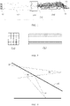
- the light-homogenized rod unit 202 is in a form a rectangular array of light-homogenized rods as shown in FIG.
- FIG. 2(a) is a front view of rectangular light-homogenized rods
- FIG. 2(b) is a side view thereof.
- Each laser device in the array of laser devices 10 corresponds to a respective one light-homogenized rod of the array of light-homogenized rods 202, and the laser device and the light-homogenized rod correspond to a respective set of pixel units of the spatial light modulator 40.
- the set of second relay lenses 203 can adopt a classic TRP (tilt & roll pixel) illumination light path.
- the set of second relay lenses 203 can be formed by a combination of different lenses, and a purpose of its design is to adjust each light beam from the light-homogenized rod unit 202 in such a manner that each beam can irradiate on the reflection device 30 at a preset light-cone angle.
- the preset light-cone angle is 34° or smaller.
- the preset light-cone angle ranges from 16° to 34°.
- the light beam irradiates on the reflection device 30 at a preset light-cone angle of 34°.
- the angle of 34° is based on the principle of optical design, and is related to a flip angle of the controllable unit of the spatial light modulator 40 and can be adapted to optical elements based on actual needs.
- the spatial light modulator 40 preferably adopts a light-cone angle of 34°, and if it is larger than 34°, the optical efficiency and the imaging quality will be influenced.
- Those skilled in the art can design various optical processing assemblies in combination with conventional technical measures, without limitation to the structure in FIG. 1 , as long as the light-cone angle of the light emitted to the reflection device 30 is 34°.
- the reflection device 30 can adopt a total internal reflection mirror, which is configured in such a manner that an angle between a light-cone of a light beam from the optical processing assembly and a light-exiting surface of the total internal reflection mirror is in a range of 17°-51° (sharp angles).
- the angle between the light-cone of the light beam and the light-exiting surface of the total internal reflection mirror can be in another range, depending on a different light-cone angle of the light beam.
- the pixel unit of the spatial light modulator 40 can be achieved by a technique such as a transmittance-variable display device, a liquid crystal display device, or a digital mirror/micromirror device (DMD).
- FIG. 4 is a schematic plan view of a spatial light modulator 40.
- the spatial light modulator 40 includes a plurality of independently addressable pixel units 401 (or DMD lenses).
- An irradiation area 001' of each light-cone reflected by the reflection device 30 corresponds to one set of pixel units.
- a set of pixel units includes one or more pixel units.
- the array of laser devices 10 is in a one-to-one mapping relationship with a working surface of the DMD that is equally divided into hundreds of parts.
- the control signal is also used to control nine pixel units 401 corresponding to an irradiation area 003'.
- the nine pixel units 401 respectively correspond to individual signal values.
- the nine pixel units 401 are controlled to have individual deflection angles or individual durations, so that light passing through each pixel unit 401 has a different brightness, light amount, or a transmittance, etc.
- the irradiation area 003' is formed by the laser 003 passing through the reflection device 30.
- One pixel unit 401 may further include independently addressable sub-pixel units 4011, which may be associated with, for example, a particular color such as red, green, and blue.
- Those skilled in the art can also use other conventional technical measures to simultaneously control at the array of laser devices 10 end and at the spatial light modulator 40 end, so that the laser beam emitted from the array of laser devices 10 can be further modulated in the spatial light modulator 40.
- An original image can be obtained by only the array of laser devices 10, and display light that is more approximate to the desired image can be obtained through further modulation by the spatial light modulator 40. This can ensure a sufficient dark image occurring in a dark area outside the area with the maximum brightness in the image, so that the dark image has a more delicate and rich image level, and thus the viewer can have a better visual experience when the display light is projected onto the screen and imaged.
- the optical path control principle of this embodiment will be briefly summarized as follows.
- the array of laser devices 10 emits light beams, and each laser device corresponds to one light-homogenized rod in the array of light-homogenized rods 202 and corresponds to a set of DMD lenses.
- the intensity of the light beam emitted from each laser device can be modulated by controlling the laser device, and the intensity of the light beam incident on the set of DMD lenses corresponding to the laser device is controlled by controlling the flip angle/duration of some or all of the DMD lenses of the set of DMD lenses, so that the light beam is reflected to the lens. That is, the laser device and the set of DMD lenses are controlled in series, and the light beam is controlled both at the laser device end and at the DMD lens end.
- a direction of a central axis between the light source device 10 and the set of first relay lenses 201 is a first direction
- a direction of a central axis between the lenses in the set of second relay lenses 203 is a second direction.
- both the first direction and the second direction each are generally designed as a horizontal direction.
- a surface of the spatial light modulator 40 for receiving the light is also in the horizontal direction.
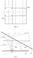
- two light beams i.e., a first light-cone 001 and a second light-cone 002
- a light axis direction of the first light-cone 001 and a light axis direction of the second light-cone 002 are also the horizontal direction.
- an apexes of the light-cones (which can be considered to have a diameter d') are not all exactly in the horizontal line. As shown in FIG.
- an irradiation area 002' on the spatial light modulator 40 formed by the second light-cone 002 overlaps exactly with a set of pixel units, and its diameter is d'.
- An irradiation area 001' on the spatial light modulator 40 formed by the first light-cone 001 is larger, and its diameter d1 is beyond the area of a set of pixel units. Therefore, this phenomenon of the display system in the related art causes a large difference in dispersion degrees of many light spots (i.e., the irradiation areas), which affects controlling the light by the spatial light modulator 40, and reduces the imaging quality.
- the array of laser devices 10 is tilted upward by a preset angle of inclination relative to the horizontal direction, for example, the array of laser devices 10 is tilted upward by 2°-3°. That is, the first direction is a direction tilted upward by 2°-3° relative to the horizontal direction, and the second direction is the horizontal direction. Then, the first light-cone 001 and the second light-cone 002 irradiate on the reflection device 30, the direction of the light axis of the first light-cone 001 and the direction of the light axis of the second light-cone 002 are also tilted upward by 2°-3° relative to the horizontal direction.
- an irradiation area on the spatial light modulator 40 formed by the second light-cone 002 overlaps exactly with a set of pixels.
- a diameter of an irradiation area on the spatial light modulator 40 formed by the first light-cone 001 is d2. It can be clearly seen that d2 is smaller than d1. In other words, compared with the related art, the display system in this embodiment has a smaller or negligible difference in dispersion degrees of the light spots on the photoelectric modulator 40, and the imaging quality is improved.
- the direction of the central axis between the lenses in the set of second relay lenses 203 may be tilted upward by a preset angle with respect to the horizontal direction, and the first direction is the horizontal direction; or the direction of the central axis between the lenses in the optical processing assembly may be tilted upward by a preset angle with respect to the horizontal direction, and the first direction is the horizontal direction; or both the first direction and the second direction are tilted upward by a preset angle, so that the direction of the light axis of the first light-cone 001 and the direction of the light axis of the second light-cone 002 are tilted upward by a preset angle relative to the horizontal direction.
- the preset angle may be tilted upward relative to the horizontal direction or may be tilted downward relative to the horizontal direction, depending on the actual configuration of the display system.
- the first direction or the second direction can be offset from the vertical direction by a preset angle, so that the direction of the light axis of the first light-cone 001 and the direction of the light axis of the second light-cone 002 are offset from the vertical direction by a preset angle.
- the display system in this embodiment can have a smaller difference in dispersion degrees of the light spots on the photoelectric modulator 40, and the imaging quality and the display effect of the image can be improved.
- the display system and the display method of the present disclosure can be used in the field of High-Dynamic Range (HDR) digital imaging and projection display technologies, for example, in a Digital Light Procession (DLP) projector using TRP illumination.
- HDR High-Dynamic Range
- DLP Digital Light Procession
- the laser source can be switched and modulated at a high speed so that each laser source can achieve a function of the first photoelectric modulator, and the laser beam emitted from the array of laser devices 10 can be further modulated at the spatial light modulator 40. That is, the HDR function can be achieved by separately controlling each laser device and the DMD local area mapped thereto, thereby emitting display light for generating a more approximate desired image.
- the present disclosure uses only one spatial light modulator, which not only simplifies the light path structure, but also avoids errors that are easily caused by controlling two spatial light modulators. In this way, it is more in line with the interests of the users, and it can ensure a sufficient dark image occurring in a dark area outside the area with the maximum brightness in the image, so that the dark image has a more delicate and rich image level, and thus the viewer can have a better visual experience.
- the problem of a large difference in dispersion degrees of the light spots on the spatial light modulator in the conventional display system is solved, thereby reducing the distortion and color deviation in the imaging of the display system.
- the brightness and the color are more uniform, and the image is more similar to the object, thereby improving the imaging quality and the display effect of the image.
- the solution of these problems can allow the technician to design a more detailed mapping relationship in the DMD working surface, and provide a better hardware support for achieving the HDR function.
- the present disclosure does not require any addition optical element or light modulator while achieving significant improvements by using the cost and condition in the related art, so the present disclosure is of great significance to the developers, manufacturers and users of display systems.
Landscapes
- Physics & Mathematics (AREA)
- General Physics & Mathematics (AREA)
- Optics & Photonics (AREA)
- Engineering & Computer Science (AREA)
- Multimedia (AREA)
- Signal Processing (AREA)
- Mechanical Light Control Or Optical Switches (AREA)
- Projection Apparatus (AREA)
- Optical Modulation, Optical Deflection, Nonlinear Optics, Optical Demodulation, Optical Logic Elements (AREA)
Description
- The present disclosure relates to the field of projection and display, and in particular, to a display system and a method.
- An existing display mainly includes a light source, a first photoelectric modulator, an imaging system, a second photoelectric modulator, a projection screen, etc. Based on an image signal, two photoelectric modulators are required to control a light beam, resulting in a complex structure and error-prone situations.
- Another display system from the prior art
US 2011/0222023 includes a light source configured to emit a plurality of light beams. The plurality of light beams enters a light-homogenized rod unit and is sent to a modulator via a set of relay lenses. - For some designs in the display device, an internal reflection prism is used to change a propagation direction of light. Since the internal reflection prism has a large light-cone angle when being spread, the resulting spherical aberration and the astigmatism will cause a large difference in dispersion degrees of light spots on the photoelectric modulator. This may result in distortion and color deviation, poor color uniformity and poor quality of image display during the system imaging.
- In a first aspect of the present disclosure, a display system is provided. The display system includes: a light source device; an optical processing assembly; a reflection device; and a light modulator. The light source device is configured to emit a plurality of light beams. The optical processing assembly is configured to perform a light path adjustment on each light beam of the plurality of light beams from the light source device in such a manner that the light beam irradiates on the reflection device at a preset light-cone angle. The reflection device is configured to reflect the plurality of light beams from the optical processing assembly to the light modulator. The light modulator includes a plurality of sets of controllable units. The reflection device is adopted to make the light beam reflected by itself illuminates on a set of controllable units. The light modulator is configured to modulate the light beam by each controllable unit, so as to emit desired display light. The light source device is characterized in that a central axis direction between the light source device and the set of first relay lenses is a first direction, and a central axis direction between lenses of the set of second relay lenses is a second direction, and the first direction and the second direction are offset from each other by a preset angle of inclination.
- In a second aspect of the present disclosure, a display method is provided. The display method includes:
- controlling the array of solid-state light sources to emit light, and controlling each solid-state light source in the array of solid-state light sources to modulate intensity of a light beam emitted from the solid-state light source; and
- controlling a flip angle/duration of one or more controllable units of the set of controllable units corresponding to the solid-state light source, thereby controlling intensity of the light beam emitted from the set of controllable units.
- In the present disclosure, by simultaneously controlling at the array of solid-state light sources end and at the spatial light modulator end, the laser beam emitted from the array of solid-state light sources is further modulated in the spatial light modulator, thereby emitting display light for generating a more approximate desired image. This can avoid errors that easily occur. By designing a preset angle of inclination, the difference in dispersion degrees of the light spots on the spatial light modulator can be reduced, thereby reducing the distortion and color deviation in imaging of the display system, and thus improving the imaging quality and the display effect of the image.
-
-
FIG. 1 is a schematic structural diagram of a display system according toEmbodiment 1 of the present disclosure; -
FIG. 2 is a schematic structural diagram of a rectangular light-homogenized rod of a display system according toEmbodiment 1 of the present disclosure; -
FIG. 3 is a schematic diagram of a light-cone angle in a display system according toEmbodiment 1 of the present disclosure; -
FIG. 4 is a diagram illustrating a correspondence between irradiation ranges of light-cone and pixel units on a spatial light modulator according toEmbodiment 1 of the present disclosure; -
FIG. 5 is a schematic diagram of light-cones irradiating a spatial light modulator in a display system according to the related art; -
FIG. 6 is a schematic diagram illustrating a difference in dispersion degrees of light spots on a spatial light modulator in a display system according to the related art; and -
FIG. 7 is a schematic diagram of light-cones irradiating a spatial light modulator in a display system according toEmbodiment 1 of the present disclosure. - The present disclosure will be further described in the following with reference to the accompanying drawings and embodiments.
- As shown in
FIG. 1 , in this embodiment, a display system includes alight source device 10, an optical processing assembly, areflection device 30, aspatial light modulator 40, a controller, and a screen. The controller is respectively connected to thelight source device 10 and thespatial light modulator 40. The optical processing assembly includes a set offirst relay lenses 201, a light-homogenized rod unit 202 and a set ofsecond relay lenses 203. - The
light source device 10 is an array of solid-state light sources for emitting a plurality of light beams. Thespatial light modulator 40 includes a plurality of controllable units, i.e., pixel units. Each solid-state light source of thelight source device 10 emits a light beam corresponding to a set of pixel units of thespatial light modulator 40. It should be noted that the solid-state light source includes a laser device and a LED. Unless otherwise specified, the laser device and array of laser devices will be described by way of an example in the following. - The principle of the display system according to the present embodiment generating display light will be described in the following.
- The controller first receives a control signal, which may be information on each pixel in one frame of image. The controller controls each laser device in the array of
laser devices 10 to emit light in accordance with the control signal. The light emitted from each laser device has an independent state. For example, each laser device can be controlled to turn on or turn off based on the control signal, or each laser device can emit laser beams having different light intensities or brightness based on the control signal. In other embodiments of the present disclosure, the light source device can also be designed as a single laser source with a light modulator. Each controllable unit of the light modulator separately modulates the laser that irradiates on it based on the control signal, until the laser emitted from the laser source is decomposed into light beams of different states. - The array of
laser devices 10 emits each laser beam to the set offirst relay lenses 201. In practical applications, considering dimensions of optical elements in the display system, laser beams emitted from the array oflaser devices 10 diverge to some extent and cannot be regarded as pure light. Correspondingly, the laser beam emitting from the optical processing assembly is in a light-cone state with a light-cone angle. The set offirst relay lenses 201 is used to converge the light beams to the light-homogenized rod unit 202. In this embodiment, the light-homogenized rod unit 202 is in a form a rectangular array of light-homogenized rods as shown inFIG. 2 , which is more advantageous for performing homogenization on each light beam from the set offirst relay lenses 201 and then transmitting the light beam to the set ofsecond relay lenses 203.FIG. 2(a) is a front view of rectangular light-homogenized rods, andFIG. 2(b) is a side view thereof. Each laser device in the array oflaser devices 10 corresponds to a respective one light-homogenized rod of the array of light-homogenized rods 202, and the laser device and the light-homogenized rod correspond to a respective set of pixel units of thespatial light modulator 40. The set ofsecond relay lenses 203 can adopt a classic TRP (tilt & roll pixel) illumination light path. The set ofsecond relay lenses 203 can be formed by a combination of different lenses, and a purpose of its design is to adjust each light beam from the light-homogenizedrod unit 202 in such a manner that each beam can irradiate on thereflection device 30 at a preset light-cone angle. Herein, the preset light-cone angle is 34° or smaller. Preferably, the preset light-cone angle ranges from 16° to 34°. For example, in this embodiment, after a series of transmission and refraction in the set ofsecond relay lenses 203, the light beam irradiates on thereflection device 30 at a preset light-cone angle of 34°. Herein, the angle of 34° is based on the principle of optical design, and is related to a flip angle of the controllable unit of the spatiallight modulator 40 and can be adapted to optical elements based on actual needs. In this embodiment, the spatiallight modulator 40 preferably adopts a light-cone angle of 34°, and if it is larger than 34°, the optical efficiency and the imaging quality will be influenced. Those skilled in the art can design various optical processing assemblies in combination with conventional technical measures, without limitation to the structure inFIG. 1 , as long as the light-cone angle of the light emitted to thereflection device 30 is 34°. - In this embodiment, as shown in
FIG. 3 , thereflection device 30 can adopt a total internal reflection mirror, which is configured in such a manner that an angle between a light-cone of a light beam from the optical processing assembly and a light-exiting surface of the total internal reflection mirror is in a range of 17°-51° (sharp angles). In other embodiments of the present disclosure, considering an overall design for the display system, the angle between the light-cone of the light beam and the light-exiting surface of the total internal reflection mirror can be in another range, depending on a different light-cone angle of the light beam. - In this embodiment, the pixel unit of the spatial light modulator 40 (SLM) can be achieved by a technique such as a transmittance-variable display device, a liquid crystal display device, or a digital mirror/micromirror device (DMD).
FIG. 4 is a schematic plan view of a spatiallight modulator 40. The spatiallight modulator 40 includes a plurality of independently addressable pixel units 401 (or DMD lenses). An irradiation area 001' of each light-cone reflected by thereflection device 30 corresponds to one set of pixel units. A set of pixel units includes one or more pixel units. The array oflaser devices 10 is in a one-to-one mapping relationship with a working surface of the DMD that is equally divided into hundreds of parts. When the controller uses a control signal to control a laser device in the array oflaser devices 10 to emitlaser 003, the control signal is also used to control ninepixel units 401 corresponding to an irradiation area 003'. The ninepixel units 401 respectively correspond to individual signal values. For example, the ninepixel units 401 are controlled to have individual deflection angles or individual durations, so that light passing through eachpixel unit 401 has a different brightness, light amount, or a transmittance, etc. The irradiation area 003' is formed by thelaser 003 passing through thereflection device 30. Onepixel unit 401 may further include independentlyaddressable sub-pixel units 4011, which may be associated with, for example, a particular color such as red, green, and blue. Those skilled in the art can also use other conventional technical measures to simultaneously control at the array oflaser devices 10 end and at the spatiallight modulator 40 end, so that the laser beam emitted from the array oflaser devices 10 can be further modulated in the spatiallight modulator 40. An original image can be obtained by only the array oflaser devices 10, and display light that is more approximate to the desired image can be obtained through further modulation by the spatiallight modulator 40. This can ensure a sufficient dark image occurring in a dark area outside the area with the maximum brightness in the image, so that the dark image has a more delicate and rich image level, and thus the viewer can have a better visual experience when the display light is projected onto the screen and imaged. - The optical path control principle of this embodiment will be briefly summarized as follows. The array of
laser devices 10 emits light beams, and each laser device corresponds to one light-homogenized rod in the array of light-homogenizedrods 202 and corresponds to a set of DMD lenses. In this embodiment, the intensity of the light beam emitted from each laser device can be modulated by controlling the laser device, and the intensity of the light beam incident on the set of DMD lenses corresponding to the laser device is controlled by controlling the flip angle/duration of some or all of the DMD lenses of the set of DMD lenses, so that the light beam is reflected to the lens. That is, the laser device and the set of DMD lenses are controlled in series, and the light beam is controlled both at the laser device end and at the DMD lens end. - A direction of a central axis between the
light source device 10 and the set offirst relay lenses 201 is a first direction, and a direction of a central axis between the lenses in the set ofsecond relay lenses 203 is a second direction. As shown inFIG. 5 , for the display system in the related art, both the first direction and the second direction each are generally designed as a horizontal direction. A surface of the spatiallight modulator 40 for receiving the light is also in the horizontal direction. For example, two light beams, i.e., a first light-cone 001 and a second light-cone 002, are emitted from the set ofsecond relay lenses 203, and a light axis direction of the first light-cone 001 and a light axis direction of the second light-cone 002 are also the horizontal direction. After the first light-cone 001 and the second light-cone 002 are reflected by thereflection device 30, an apexes of the light-cones (which can be considered to have a diameter d') are not all exactly in the horizontal line. As shown inFIG. 6 , considering the second light-cone 002 as an ideal case, an irradiation area 002' on the spatiallight modulator 40 formed by the second light-cone 002 overlaps exactly with a set of pixel units, and its diameter is d'. An irradiation area 001' on the spatiallight modulator 40 formed by the first light-cone 001 is larger, and its diameter d1 is beyond the area of a set of pixel units. Therefore, this phenomenon of the display system in the related art causes a large difference in dispersion degrees of many light spots (i.e., the irradiation areas), which affects controlling the light by the spatiallight modulator 40, and reduces the imaging quality. - As shown in
FIG. 7 , in this embodiment, the array oflaser devices 10 is tilted upward by a preset angle of inclination relative to the horizontal direction, for example, the array oflaser devices 10 is tilted upward by 2°-3°. That is, the first direction is a direction tilted upward by 2°-3° relative to the horizontal direction, and the second direction is the horizontal direction. Then, the first light-cone 001 and the second light-cone 002 irradiate on thereflection device 30, the direction of the light axis of the first light-cone 001 and the direction of the light axis of the second light-cone 002 are also tilted upward by 2°-3° relative to the horizontal direction. After the first light-cone 001 and the second light-cone 002 are reflected onto the spatiallight modulator 40, considering the second light-cone 002 as an ideal case, an irradiation area on the spatiallight modulator 40 formed by the second light-cone 002 overlaps exactly with a set of pixels. A diameter of an irradiation area on the spatiallight modulator 40 formed by the first light-cone 001 is d2. It can be clearly seen that d2 is smaller than d1. In other words, compared with the related art, the display system in this embodiment has a smaller or negligible difference in dispersion degrees of the light spots on thephotoelectric modulator 40, and the imaging quality is improved. In other embodiments of the present disclosure, the direction of the central axis between the lenses in the set ofsecond relay lenses 203, i.e., the second direction, may be tilted upward by a preset angle with respect to the horizontal direction, and the first direction is the horizontal direction; or the direction of the central axis between the lenses in the optical processing assembly may be tilted upward by a preset angle with respect to the horizontal direction, and the first direction is the horizontal direction; or both the first direction and the second direction are tilted upward by a preset angle, so that the direction of the light axis of the first light-cone 001 and the direction of the light axis of the second light-cone 002 are tilted upward by a preset angle relative to the horizontal direction. Moreover, the preset angle may be tilted upward relative to the horizontal direction or may be tilted downward relative to the horizontal direction, depending on the actual configuration of the display system. When the display system as a whole is not horizontally but vertically disposed, the first direction or the second direction can be offset from the vertical direction by a preset angle, so that the direction of the light axis of the first light-cone 001 and the direction of the light axis of the second light-cone 002 are offset from the vertical direction by a preset angle. In this way, compared with the related art, the display system in this embodiment can have a smaller difference in dispersion degrees of the light spots on thephotoelectric modulator 40, and the imaging quality and the display effect of the image can be improved. - The display system and the display method of the present disclosure can be used in the field of High-Dynamic Range (HDR) digital imaging and projection display technologies, for example, in a Digital Light Procession (DLP) projector using TRP illumination. By simultaneously controlling at the array of
laser devices 10 end and at the spatiallight modulator 40 end, the laser source can be switched and modulated at a high speed so that each laser source can achieve a function of the first photoelectric modulator, and the laser beam emitted from the array oflaser devices 10 can be further modulated at the spatiallight modulator 40. That is, the HDR function can be achieved by separately controlling each laser device and the DMD local area mapped thereto, thereby emitting display light for generating a more approximate desired image. In this way, the viewer can have a better visual experience when the display light is projected onto the screen. At the same time, compared with the related art in which two spatial light modulators are used, the present disclosure uses only one spatial light modulator, which not only simplifies the light path structure, but also avoids errors that are easily caused by controlling two spatial light modulators. In this way, it is more in line with the interests of the users, and it can ensure a sufficient dark image occurring in a dark area outside the area with the maximum brightness in the image, so that the dark image has a more delicate and rich image level, and thus the viewer can have a better visual experience. Moreover, with the present disclosure, the problem of a large difference in dispersion degrees of the light spots on the spatial light modulator in the conventional display system is solved, thereby reducing the distortion and color deviation in the imaging of the display system. As a result, the brightness and the color are more uniform, and the image is more similar to the object, thereby improving the imaging quality and the display effect of the image. The solution of these problems can allow the technician to design a more detailed mapping relationship in the DMD working surface, and provide a better hardware support for achieving the HDR function. The present disclosure does not require any addition optical element or light modulator while achieving significant improvements by using the cost and condition in the related art, so the present disclosure is of great significance to the developers, manufacturers and users of display systems.
Claims (10)
- A display system, comprising:a light source device (10);an optical processing assembly;a reflection device (30); anda light modulator (40);wherein the light source device is configured to emit a plurality of light beams,the optical processing assembly comprises a set of first relay lenses, lenses (201);a light-homogenized rod unit (202) and a set of second relay lenses, lenses (203); wherein the set of first relay lenses is configured to converge the plurality of light beams from the light source device to the light-homogenized rod unit, the light-homogenized rod unit is configured to perform homogenization on each light beam from the set of first relay lenses and transmit the light beam to the set of second relay lenses, and the set of second relay lenses is configured to adjust each light beam from the light-homogenized rod unit such that each light beam is irradiated on the reflection device in a preset light-cone angle,the reflection device is configured to reflect the plurality of light beams from the optical processing assembly to the light modulator, andthe light modulator comprises a plurality of sets of controllable units, each light beam reflected by the reflection device corresponds to a respective set of the plurality of sets of controllable units, and the light modulator is configured to control one or more controllable units in the respective set of controllable units to modulate the light beam corresponding to the set of controllable units, so as to emit desired display light,characterized in that a central axis direction between the light source device and the set of first relay lenses is a first direction, and a central axis direction between lenses of the set of second relay lenses is a second direction, and the first direction and the second direction are offset from each other by a preset angle of inclination.
- The display system according to claim 1, characterized in that the light source device comprises an array of solid-state light sources (10) configured to emit a plurality of laser beam: (003) and a laser beam emitted from each solid-state light source in the array of solid-state light sources corresponds to one set of the plurality of sets of controllable units of the light modulator.
- The display system according to claim 2, characterized in further comprising:a controller connected to the light source device and the light modulator,wherein the controller is configured to receive a control signal, control a light emission state of a solid-state light source in the array of solid-state light sources in accordance with the control signal, and control a modulation state of one or more controllable units of the set of controllable units corresponding to the solid-state light source, such that the light modulator modulates the light beam emitted from the solid-state light source and emit desired display light in accordance with the control signal.
- The display system according to claim 1, characterized in that the light-homogenized rod unit (202) is a rectangular array of light-homogenized rods, and each light source in the array of solid-state light sources is in one-to-one correspondence to a respective light-homogenized rod of the array of light-homogenized rods, and the solid-state light source and the light-homogenized rod correspond to a respective set of controllable units (401) of the light modulator.
- The display system according to claim 1, characterized in that the preset light-cone angle is in a range of 16°-34°.
- The display system according to any one of claims 1-3, characterized in that the reflection device (30) is disposed in such a manner that an angle between a light beam in a form of a light-cone from the optical processing assembly and a light-exiting surface of the reflection device is in a range of 17°-51°.
- The display system according to any one of claims 1-3, characterized in further comprising a projection screen configured to receive display light from the light modulator so as to display an image.
- The display system according to claim 1, characterized in that the first direction and the second direction are offset from each other by 2°-3°.
- The display system according to claim 1, characterized in that the first direction is a horizontal/vertical direction, and the second direction is offset from the horizontal/vertical direction by the preset angle of inclination; or the second direction is a horizontal/vertical direction, and the first direction is offset from the horizontal/vertical direction by the preset angle of inclination.
- A display method, characterized in using the display system according to any one of claims 1-9, wherein the display method comprises:controlling the array of solid-state light sources (10) to emit light, and controlling each solid-state light source in the array of solid-state light sources to modulate intensity of a light beam emitted from the solid-state light source; andcontrolling a flip angle/duration of one or more controllable units (401)of the set of controllable units corresponding to the solid-state light source, thereby controlling intensity of the light beam emitted from the set of controllable units.
Applications Claiming Priority (2)
| Application Number | Priority Date | Filing Date | Title |
|---|---|---|---|
| CN201610519561.1A CN107577108B (en) | 2016-07-04 | 2016-07-04 | A kind of display system and method |
| PCT/CN2017/082409 WO2018006638A1 (en) | 2016-07-04 | 2017-04-28 | Display system and method |
Publications (3)
| Publication Number | Publication Date |
|---|---|
| EP3480656A1 EP3480656A1 (en) | 2019-05-08 |
| EP3480656A4 EP3480656A4 (en) | 2020-03-11 |
| EP3480656B1 true EP3480656B1 (en) | 2022-10-12 |
Family
ID=60901701
Family Applications (1)
| Application Number | Title | Priority Date | Filing Date |
|---|---|---|---|
| EP17823450.6A Active EP3480656B1 (en) | 2016-07-04 | 2017-04-28 | Display system and method |
Country Status (4)
| Country | Link |
|---|---|
| US (1) | US11003064B2 (en) |
| EP (1) | EP3480656B1 (en) |
| CN (1) | CN107577108B (en) |
| WO (1) | WO2018006638A1 (en) |
Families Citing this family (1)
| Publication number | Priority date | Publication date | Assignee | Title |
|---|---|---|---|---|
| CN113038103A (en) * | 2021-03-22 | 2021-06-25 | 青岛海信激光显示股份有限公司 | Laser projection host applied to laser display equipment and laser display equipment |
Family Cites Families (29)
| Publication number | Priority date | Publication date | Assignee | Title |
|---|---|---|---|---|
| JPH10254370A (en) * | 1997-03-10 | 1998-09-25 | Canon Inc | Display panel and projection type display device using it |
| KR100493839B1 (en) * | 2000-03-14 | 2005-06-10 | 미쓰비시덴키 가부시키가이샤 | An image display apparatus and an image display method |
| JP2002350775A (en) * | 2001-05-30 | 2002-12-04 | Fuji Photo Optical Co Ltd | Projector |
| ES2675880T3 (en) * | 2002-03-13 | 2018-07-13 | Dolby Laboratories Licensing Corporation | Failure compensation of light emitting element on a monitor |
| US6724546B2 (en) * | 2002-04-25 | 2004-04-20 | Mitsubishi Denki Kabushiki Kaisha | Light converging optical system for converging light onto a reflecting optical-spatial modulator element and image displaying apparatus for displaying an image formed by light reflected by the reflecting optical-spatial modulator element |
| CN1383034A (en) | 2002-05-24 | 2002-12-04 | 杭州浙大科特光电科技有限公司 | Optical engine of back-projecting liquid crystal TV set |
| JP4082332B2 (en) * | 2003-04-11 | 2008-04-30 | セイコーエプソン株式会社 | Display device and projector |
| CN100410722C (en) * | 2003-06-02 | 2008-08-13 | 明锐有限公司 | Manufacture of high fill ratio reflective spatial light modulator with hidden hinge |
| KR100677551B1 (en) | 2005-01-05 | 2007-02-02 | 삼성전자주식회사 | LED package, illumination system and projection system employing the LED package |
| CN1847975A (en) * | 2005-04-05 | 2006-10-18 | 中强光电股份有限公司 | Light source device of projector |
| CN101109488A (en) * | 2007-08-23 | 2008-01-23 | 福州高意光学有限公司 | Multiple primary color LED luminous structure and application in projector and lighting system |
| CN101387815B (en) * | 2007-09-12 | 2010-09-29 | 鸿富锦精密工业(深圳)有限公司 | Projector |
| US8451427B2 (en) * | 2007-09-14 | 2013-05-28 | Nikon Corporation | Illumination optical system, exposure apparatus, optical element and manufacturing method thereof, and device manufacturing method |
| CN101424768A (en) * | 2007-11-02 | 2009-05-06 | 北京京东方光电科技有限公司 | Light guide board, back light source and LCD |
| US7551341B1 (en) | 2008-01-28 | 2009-06-23 | Dolby Laboratories Licensing Corporation | Serial modulation display having binary light modulation stage |
| CN102239445A (en) * | 2008-12-05 | 2011-11-09 | 三洋电机株式会社 | Lighting device and projection type video display device |
| WO2012139634A1 (en) * | 2011-04-12 | 2012-10-18 | Barco N.V. | Laser projector with reduced speckle |
| CN102269920B (en) * | 2011-07-21 | 2013-01-23 | 凝辉(天津)科技有限责任公司 | Separable micro laser projection device |
| WO2013070514A2 (en) * | 2011-11-08 | 2013-05-16 | Reald Inc. | Imaging path speckle mitigation |
| US8860640B2 (en) | 2012-05-30 | 2014-10-14 | Christie Digital Systems Usa, Inc. | Zonal illumination for high dynamic range projection |
| JP5910324B2 (en) * | 2012-06-04 | 2016-04-27 | ソニー株式会社 | Illumination device, projection display device, and direct view display device |
| CN103913937B (en) * | 2013-01-01 | 2016-04-20 | 深圳市光峰光电技术有限公司 | Light-emitting device and relevant projecting system thereof |
| CN104049445B (en) * | 2013-03-11 | 2016-12-28 | 深圳市绎立锐光科技开发有限公司 | Light-emitting device and optical projection system |
| KR20150114763A (en) | 2014-04-02 | 2015-10-13 | 삼성전자주식회사 | Projector |
| CN104062838A (en) * | 2014-07-08 | 2014-09-24 | 深圳市安华光电技术有限公司 | Interactive projection optical system and working method thereof |
| CN105334687B (en) | 2014-08-01 | 2019-04-12 | 欧司朗股份有限公司 | Optical projection system |
| CN204178113U (en) * | 2014-10-31 | 2015-02-25 | 深圳市绎立锐光科技开发有限公司 | Light-emitting device and there is its projector |
| WO2017013706A1 (en) * | 2015-07-17 | 2017-01-26 | Necディスプレイソリューションズ株式会社 | Image display device and image display method |
| CN205984148U (en) * | 2016-07-04 | 2017-02-22 | 深圳市光峰光电技术有限公司 | Display system |
-
2016
- 2016-07-04 CN CN201610519561.1A patent/CN107577108B/en active Active
-
2017
- 2017-04-28 US US16/314,899 patent/US11003064B2/en active Active
- 2017-04-28 EP EP17823450.6A patent/EP3480656B1/en active Active
- 2017-04-28 WO PCT/CN2017/082409 patent/WO2018006638A1/en unknown
Also Published As
| Publication number | Publication date |
|---|---|
| CN107577108B (en) | 2019-09-20 |
| EP3480656A1 (en) | 2019-05-08 |
| WO2018006638A1 (en) | 2018-01-11 |
| US20190155137A1 (en) | 2019-05-23 |
| EP3480656A4 (en) | 2020-03-11 |
| CN107577108A (en) | 2018-01-12 |
| US11003064B2 (en) | 2021-05-11 |
Similar Documents
| Publication | Publication Date | Title |
|---|---|---|
| JP7108770B2 (en) | Method and system for high dynamic range image projector | |
| EP2670144B1 (en) | Zonal illumination for high dynamic range projection | |
| EP2869570B1 (en) | Two-stage light modulation for high dynamic range | |
| JP2004523001A5 (en) | ||
| TW201602556A (en) | Camera shooting method achieved through camera shooting elements | |
| CN102914938B (en) | Projector | |
| JP2009037259A (en) | High dynamic range display device | |
| JP2009186923A (en) | Illuminating device, illuminating method, image signal processing device, image signal processing method, and image projecting device | |
| US20160327783A1 (en) | Projection display system and method | |
| CN107797368B (en) | Dual spatial light modulation system and method for light modulation using the same | |
| US20230098832A1 (en) | Laser projection device and projection display method thereof | |
| JP2014178686A5 (en) | ||
| CN110855968A (en) | Projection display apparatus using self-luminous pixel array device | |
| CN112637576A (en) | Projection apparatus and projection control method | |
| EP3480656B1 (en) | Display system and method | |
| CN110876045B (en) | Projection method and projector | |
| EP3848753B1 (en) | Light source system and control method thereof, display device and control method thereof | |
| CN205984148U (en) | Display system | |
| CN105980927A (en) | Acousto-optic beam steering modulator for a projection system | |
| KR101419966B1 (en) | Projection image display device having two modulation stages, including one aperture modulation stage | |
| CN113031257B (en) | Display system | |
| EP3931607A1 (en) | Method and system for spatial and angular uniformization of light beams | |
| CN210431678U (en) | Projection display apparatus using self-luminous pixel array device | |
| KR19980040064A (en) | Optical Projection System and Light Projection Method Using The Same | |
| JP2023529104A (en) | Projection system with rotatable anamorphic lens |
Legal Events
| Date | Code | Title | Description |
|---|---|---|---|
| STAA | Information on the status of an ep patent application or granted ep patent |
Free format text: STATUS: THE INTERNATIONAL PUBLICATION HAS BEEN MADE |
|
| PUAI | Public reference made under article 153(3) epc to a published international application that has entered the european phase |
Free format text: ORIGINAL CODE: 0009012 |
|
| STAA | Information on the status of an ep patent application or granted ep patent |
Free format text: STATUS: REQUEST FOR EXAMINATION WAS MADE |
|
| STAA | Information on the status of an ep patent application or granted ep patent |
Free format text: STATUS: REQUEST FOR EXAMINATION WAS MADE |
|
| 17P | Request for examination filed |
Effective date: 20190115 |
|
| AK | Designated contracting states |
Kind code of ref document: A1 Designated state(s): AL AT BE BG CH CY CZ DE DK EE ES FI FR GB GR HR HU IE IS IT LI LT LU LV MC MK MT NL NO PL PT RO RS SE SI SK SM TR |
|
| AX | Request for extension of the european patent |
Extension state: BA ME |
|
| DAV | Request for validation of the european patent (deleted) | ||
| DAX | Request for extension of the european patent (deleted) | ||
| A4 | Supplementary search report drawn up and despatched |
Effective date: 20200212 |
|
| RIC1 | Information provided on ipc code assigned before grant |
Ipc: G03B 21/20 20060101AFI20200206BHEP |
|
| GRAP | Despatch of communication of intention to grant a patent |
Free format text: ORIGINAL CODE: EPIDOSNIGR1 |
|
| STAA | Information on the status of an ep patent application or granted ep patent |
Free format text: STATUS: GRANT OF PATENT IS INTENDED |
|
| INTG | Intention to grant announced |
Effective date: 20220512 |
|
| GRAS | Grant fee paid |
Free format text: ORIGINAL CODE: EPIDOSNIGR3 |
|
| GRAA | (expected) grant |
Free format text: ORIGINAL CODE: 0009210 |
|
| STAA | Information on the status of an ep patent application or granted ep patent |
Free format text: STATUS: THE PATENT HAS BEEN GRANTED |
|
| AK | Designated contracting states |
Kind code of ref document: B1 Designated state(s): AL AT BE BG CH CY CZ DE DK EE ES FI FR GB GR HR HU IE IS IT LI LT LU LV MC MK MT NL NO PL PT RO RS SE SI SK SM TR |
|
| REG | Reference to a national code |
Ref country code: GB Ref legal event code: FG4D |
|
| REG | Reference to a national code |
Ref country code: CH Ref legal event code: EP |
|
| REG | Reference to a national code |
Ref country code: DE Ref legal event code: R096 Ref document number: 602017062632 Country of ref document: DE |
|
| REG | Reference to a national code |
Ref country code: IE Ref legal event code: FG4D |
|
| REG | Reference to a national code |
Ref country code: AT Ref legal event code: REF Ref document number: 1524523 Country of ref document: AT Kind code of ref document: T Effective date: 20221115 |
|
| REG | Reference to a national code |
Ref country code: LT Ref legal event code: MG9D |
|
| REG | Reference to a national code |
Ref country code: NL Ref legal event code: MP Effective date: 20221012 |
|
| REG | Reference to a national code |
Ref country code: AT Ref legal event code: MK05 Ref document number: 1524523 Country of ref document: AT Kind code of ref document: T Effective date: 20221012 |
|
| PG25 | Lapsed in a contracting state [announced via postgrant information from national office to epo] |
Ref country code: NL Free format text: LAPSE BECAUSE OF FAILURE TO SUBMIT A TRANSLATION OF THE DESCRIPTION OR TO PAY THE FEE WITHIN THE PRESCRIBED TIME-LIMIT Effective date: 20221012 |
|
| PG25 | Lapsed in a contracting state [announced via postgrant information from national office to epo] |
Ref country code: SE Free format text: LAPSE BECAUSE OF FAILURE TO SUBMIT A TRANSLATION OF THE DESCRIPTION OR TO PAY THE FEE WITHIN THE PRESCRIBED TIME-LIMIT Effective date: 20221012 Ref country code: PT Free format text: LAPSE BECAUSE OF FAILURE TO SUBMIT A TRANSLATION OF THE DESCRIPTION OR TO PAY THE FEE WITHIN THE PRESCRIBED TIME-LIMIT Effective date: 20230213 Ref country code: NO Free format text: LAPSE BECAUSE OF FAILURE TO SUBMIT A TRANSLATION OF THE DESCRIPTION OR TO PAY THE FEE WITHIN THE PRESCRIBED TIME-LIMIT Effective date: 20230112 Ref country code: LT Free format text: LAPSE BECAUSE OF FAILURE TO SUBMIT A TRANSLATION OF THE DESCRIPTION OR TO PAY THE FEE WITHIN THE PRESCRIBED TIME-LIMIT Effective date: 20221012 Ref country code: FI Free format text: LAPSE BECAUSE OF FAILURE TO SUBMIT A TRANSLATION OF THE DESCRIPTION OR TO PAY THE FEE WITHIN THE PRESCRIBED TIME-LIMIT Effective date: 20221012 Ref country code: ES Free format text: LAPSE BECAUSE OF FAILURE TO SUBMIT A TRANSLATION OF THE DESCRIPTION OR TO PAY THE FEE WITHIN THE PRESCRIBED TIME-LIMIT Effective date: 20221012 Ref country code: AT Free format text: LAPSE BECAUSE OF FAILURE TO SUBMIT A TRANSLATION OF THE DESCRIPTION OR TO PAY THE FEE WITHIN THE PRESCRIBED TIME-LIMIT Effective date: 20221012 |
|
| PG25 | Lapsed in a contracting state [announced via postgrant information from national office to epo] |
Ref country code: RS Free format text: LAPSE BECAUSE OF FAILURE TO SUBMIT A TRANSLATION OF THE DESCRIPTION OR TO PAY THE FEE WITHIN THE PRESCRIBED TIME-LIMIT Effective date: 20221012 Ref country code: PL Free format text: LAPSE BECAUSE OF FAILURE TO SUBMIT A TRANSLATION OF THE DESCRIPTION OR TO PAY THE FEE WITHIN THE PRESCRIBED TIME-LIMIT Effective date: 20221012 Ref country code: LV Free format text: LAPSE BECAUSE OF FAILURE TO SUBMIT A TRANSLATION OF THE DESCRIPTION OR TO PAY THE FEE WITHIN THE PRESCRIBED TIME-LIMIT Effective date: 20221012 Ref country code: IS Free format text: LAPSE BECAUSE OF FAILURE TO SUBMIT A TRANSLATION OF THE DESCRIPTION OR TO PAY THE FEE WITHIN THE PRESCRIBED TIME-LIMIT Effective date: 20230212 Ref country code: HR Free format text: LAPSE BECAUSE OF FAILURE TO SUBMIT A TRANSLATION OF THE DESCRIPTION OR TO PAY THE FEE WITHIN THE PRESCRIBED TIME-LIMIT Effective date: 20221012 Ref country code: GR Free format text: LAPSE BECAUSE OF FAILURE TO SUBMIT A TRANSLATION OF THE DESCRIPTION OR TO PAY THE FEE WITHIN THE PRESCRIBED TIME-LIMIT Effective date: 20230113 |
|
| REG | Reference to a national code |
Ref country code: DE Ref legal event code: R097 Ref document number: 602017062632 Country of ref document: DE |
|
| PG25 | Lapsed in a contracting state [announced via postgrant information from national office to epo] |
Ref country code: SM Free format text: LAPSE BECAUSE OF FAILURE TO SUBMIT A TRANSLATION OF THE DESCRIPTION OR TO PAY THE FEE WITHIN THE PRESCRIBED TIME-LIMIT Effective date: 20221012 Ref country code: RO Free format text: LAPSE BECAUSE OF FAILURE TO SUBMIT A TRANSLATION OF THE DESCRIPTION OR TO PAY THE FEE WITHIN THE PRESCRIBED TIME-LIMIT Effective date: 20221012 Ref country code: EE Free format text: LAPSE BECAUSE OF FAILURE TO SUBMIT A TRANSLATION OF THE DESCRIPTION OR TO PAY THE FEE WITHIN THE PRESCRIBED TIME-LIMIT Effective date: 20221012 Ref country code: DK Free format text: LAPSE BECAUSE OF FAILURE TO SUBMIT A TRANSLATION OF THE DESCRIPTION OR TO PAY THE FEE WITHIN THE PRESCRIBED TIME-LIMIT Effective date: 20221012 Ref country code: CZ Free format text: LAPSE BECAUSE OF FAILURE TO SUBMIT A TRANSLATION OF THE DESCRIPTION OR TO PAY THE FEE WITHIN THE PRESCRIBED TIME-LIMIT Effective date: 20221012 |
|
| PGFP | Annual fee paid to national office [announced via postgrant information from national office to epo] |
Ref country code: FR Payment date: 20230425 Year of fee payment: 7 Ref country code: DE Payment date: 20230412 Year of fee payment: 7 |
|
| PLBE | No opposition filed within time limit |
Free format text: ORIGINAL CODE: 0009261 |
|
| STAA | Information on the status of an ep patent application or granted ep patent |
Free format text: STATUS: NO OPPOSITION FILED WITHIN TIME LIMIT |
|
| PG25 | Lapsed in a contracting state [announced via postgrant information from national office to epo] |
Ref country code: SK Free format text: LAPSE BECAUSE OF FAILURE TO SUBMIT A TRANSLATION OF THE DESCRIPTION OR TO PAY THE FEE WITHIN THE PRESCRIBED TIME-LIMIT Effective date: 20221012 Ref country code: AL Free format text: LAPSE BECAUSE OF FAILURE TO SUBMIT A TRANSLATION OF THE DESCRIPTION OR TO PAY THE FEE WITHIN THE PRESCRIBED TIME-LIMIT Effective date: 20221012 |
|
| 26N | No opposition filed |
Effective date: 20230713 |
|
| PGFP | Annual fee paid to national office [announced via postgrant information from national office to epo] |
Ref country code: GB Payment date: 20230424 Year of fee payment: 7 |
|
| PG25 | Lapsed in a contracting state [announced via postgrant information from national office to epo] |
Ref country code: SI Free format text: LAPSE BECAUSE OF FAILURE TO SUBMIT A TRANSLATION OF THE DESCRIPTION OR TO PAY THE FEE WITHIN THE PRESCRIBED TIME-LIMIT Effective date: 20221012 |
|
| REG | Reference to a national code |
Ref country code: CH Ref legal event code: PL |
|
| PG25 | Lapsed in a contracting state [announced via postgrant information from national office to epo] |
Ref country code: LU Free format text: LAPSE BECAUSE OF NON-PAYMENT OF DUE FEES Effective date: 20230428 |
|
| REG | Reference to a national code |
Ref country code: BE Ref legal event code: MM Effective date: 20230430 |
|
| PG25 | Lapsed in a contracting state [announced via postgrant information from national office to epo] |
Ref country code: MC Free format text: LAPSE BECAUSE OF FAILURE TO SUBMIT A TRANSLATION OF THE DESCRIPTION OR TO PAY THE FEE WITHIN THE PRESCRIBED TIME-LIMIT Effective date: 20221012 |
|
| PG25 | Lapsed in a contracting state [announced via postgrant information from national office to epo] |
Ref country code: MC Free format text: LAPSE BECAUSE OF FAILURE TO SUBMIT A TRANSLATION OF THE DESCRIPTION OR TO PAY THE FEE WITHIN THE PRESCRIBED TIME-LIMIT Effective date: 20221012 Ref country code: LI Free format text: LAPSE BECAUSE OF NON-PAYMENT OF DUE FEES Effective date: 20230430 Ref country code: CH Free format text: LAPSE BECAUSE OF NON-PAYMENT OF DUE FEES Effective date: 20230430 |
|
| REG | Reference to a national code |
Ref country code: IE Ref legal event code: MM4A |
|
| PG25 | Lapsed in a contracting state [announced via postgrant information from national office to epo] |
Ref country code: BE Free format text: LAPSE BECAUSE OF NON-PAYMENT OF DUE FEES Effective date: 20230430 |
|
| PG25 | Lapsed in a contracting state [announced via postgrant information from national office to epo] |
Ref country code: IE Free format text: LAPSE BECAUSE OF NON-PAYMENT OF DUE FEES Effective date: 20230428 |
|
| PG25 | Lapsed in a contracting state [announced via postgrant information from national office to epo] |
Ref country code: IE Free format text: LAPSE BECAUSE OF NON-PAYMENT OF DUE FEES Effective date: 20230428 |