EP3480278A1 - Compound for organic optoelectronic device, composition for organic optoelectronic device, organic optoelectronic device and display apparatus - Google Patents
Compound for organic optoelectronic device, composition for organic optoelectronic device, organic optoelectronic device and display apparatus Download PDFInfo
- Publication number
- EP3480278A1 EP3480278A1 EP17820373.3A EP17820373A EP3480278A1 EP 3480278 A1 EP3480278 A1 EP 3480278A1 EP 17820373 A EP17820373 A EP 17820373A EP 3480278 A1 EP3480278 A1 EP 3480278A1
- Authority
- EP
- European Patent Office
- Prior art keywords
- group
- substituted
- unsubstituted
- compound
- optoelectronic device
- Prior art date
- Legal status (The legal status is an assumption and is not a legal conclusion. Google has not performed a legal analysis and makes no representation as to the accuracy of the status listed.)
- Granted
Links
- 0 C=*C[n]1c2ccccc2c2ccccc12 Chemical compound C=*C[n]1c2ccccc2c2ccccc12 0.000 description 1
- UHOVQNZJYSORNB-UHFFFAOYSA-N c1ccccc1 Chemical compound c1ccccc1 UHOVQNZJYSORNB-UHFFFAOYSA-N 0.000 description 1
Images

Classifications
-
- C—CHEMISTRY; METALLURGY
- C07—ORGANIC CHEMISTRY
- C07D—HETEROCYCLIC COMPOUNDS
- C07D251/00—Heterocyclic compounds containing 1,3,5-triazine rings
- C07D251/02—Heterocyclic compounds containing 1,3,5-triazine rings not condensed with other rings
- C07D251/12—Heterocyclic compounds containing 1,3,5-triazine rings not condensed with other rings having three double bonds between ring members or between ring members and non-ring members
- C07D251/14—Heterocyclic compounds containing 1,3,5-triazine rings not condensed with other rings having three double bonds between ring members or between ring members and non-ring members with hydrogen or carbon atoms directly attached to at least one ring carbon atom
- C07D251/24—Heterocyclic compounds containing 1,3,5-triazine rings not condensed with other rings having three double bonds between ring members or between ring members and non-ring members with hydrogen or carbon atoms directly attached to at least one ring carbon atom to three ring carbon atoms
-
- C—CHEMISTRY; METALLURGY
- C07—ORGANIC CHEMISTRY
- C07D—HETEROCYCLIC COMPOUNDS
- C07D209/00—Heterocyclic compounds containing five-membered rings, condensed with other rings, with one nitrogen atom as the only ring hetero atom
- C07D209/56—Ring systems containing three or more rings
- C07D209/80—[b, c]- or [b, d]-condensed
- C07D209/82—Carbazoles; Hydrogenated carbazoles
- C07D209/86—Carbazoles; Hydrogenated carbazoles with only hydrogen atoms, hydrocarbon or substituted hydrocarbon radicals, directly attached to carbon atoms of the ring system
-
- C—CHEMISTRY; METALLURGY
- C07—ORGANIC CHEMISTRY
- C07D—HETEROCYCLIC COMPOUNDS
- C07D307/00—Heterocyclic compounds containing five-membered rings having one oxygen atom as the only ring hetero atom
- C07D307/77—Heterocyclic compounds containing five-membered rings having one oxygen atom as the only ring hetero atom ortho- or peri-condensed with carbocyclic rings or ring systems
- C07D307/91—Dibenzofurans; Hydrogenated dibenzofurans
-
- C—CHEMISTRY; METALLURGY
- C07—ORGANIC CHEMISTRY
- C07D—HETEROCYCLIC COMPOUNDS
- C07D333/00—Heterocyclic compounds containing five-membered rings having one sulfur atom as the only ring hetero atom
- C07D333/50—Heterocyclic compounds containing five-membered rings having one sulfur atom as the only ring hetero atom condensed with carbocyclic rings or ring systems
- C07D333/76—Dibenzothiophenes
-
- C—CHEMISTRY; METALLURGY
- C07—ORGANIC CHEMISTRY
- C07D—HETEROCYCLIC COMPOUNDS
- C07D405/00—Heterocyclic compounds containing both one or more hetero rings having oxygen atoms as the only ring hetero atoms, and one or more rings having nitrogen as the only ring hetero atom
- C07D405/14—Heterocyclic compounds containing both one or more hetero rings having oxygen atoms as the only ring hetero atoms, and one or more rings having nitrogen as the only ring hetero atom containing three or more hetero rings
-
- C—CHEMISTRY; METALLURGY
- C07—ORGANIC CHEMISTRY
- C07D—HETEROCYCLIC COMPOUNDS
- C07D409/00—Heterocyclic compounds containing two or more hetero rings, at least one ring having sulfur atoms as the only ring hetero atoms
- C07D409/14—Heterocyclic compounds containing two or more hetero rings, at least one ring having sulfur atoms as the only ring hetero atoms containing three or more hetero rings
-
- C—CHEMISTRY; METALLURGY
- C09—DYES; PAINTS; POLISHES; NATURAL RESINS; ADHESIVES; COMPOSITIONS NOT OTHERWISE PROVIDED FOR; APPLICATIONS OF MATERIALS NOT OTHERWISE PROVIDED FOR
- C09K—MATERIALS FOR MISCELLANEOUS APPLICATIONS, NOT PROVIDED FOR ELSEWHERE
- C09K11/00—Luminescent materials, e.g. electroluminescent or chemiluminescent
- C09K11/02—Use of particular materials as binders, particle coatings or suspension media therefor
-
- C—CHEMISTRY; METALLURGY
- C09—DYES; PAINTS; POLISHES; NATURAL RESINS; ADHESIVES; COMPOSITIONS NOT OTHERWISE PROVIDED FOR; APPLICATIONS OF MATERIALS NOT OTHERWISE PROVIDED FOR
- C09K—MATERIALS FOR MISCELLANEOUS APPLICATIONS, NOT PROVIDED FOR ELSEWHERE
- C09K11/00—Luminescent materials, e.g. electroluminescent or chemiluminescent
- C09K11/06—Luminescent materials, e.g. electroluminescent or chemiluminescent containing organic luminescent materials
-
- H—ELECTRICITY
- H10—SEMICONDUCTOR DEVICES; ELECTRIC SOLID-STATE DEVICES NOT OTHERWISE PROVIDED FOR
- H10K—ORGANIC ELECTRIC SOLID-STATE DEVICES
- H10K50/00—Organic light-emitting devices
-
- H—ELECTRICITY
- H10—SEMICONDUCTOR DEVICES; ELECTRIC SOLID-STATE DEVICES NOT OTHERWISE PROVIDED FOR
- H10K—ORGANIC ELECTRIC SOLID-STATE DEVICES
- H10K50/00—Organic light-emitting devices
- H10K50/10—OLEDs or polymer light-emitting diodes [PLED]
- H10K50/14—Carrier transporting layers
- H10K50/15—Hole transporting layers
-
- H—ELECTRICITY
- H10—SEMICONDUCTOR DEVICES; ELECTRIC SOLID-STATE DEVICES NOT OTHERWISE PROVIDED FOR
- H10K—ORGANIC ELECTRIC SOLID-STATE DEVICES
- H10K50/00—Organic light-emitting devices
- H10K50/10—OLEDs or polymer light-emitting diodes [PLED]
- H10K50/14—Carrier transporting layers
- H10K50/16—Electron transporting layers
- H10K50/166—Electron transporting layers comprising a multilayered structure
-
- H—ELECTRICITY
- H10—SEMICONDUCTOR DEVICES; ELECTRIC SOLID-STATE DEVICES NOT OTHERWISE PROVIDED FOR
- H10K—ORGANIC ELECTRIC SOLID-STATE DEVICES
- H10K85/00—Organic materials used in the body or electrodes of devices covered by this subclass
- H10K85/60—Organic compounds having low molecular weight
- H10K85/649—Aromatic compounds comprising a hetero atom
- H10K85/654—Aromatic compounds comprising a hetero atom comprising only nitrogen as heteroatom
-
- H—ELECTRICITY
- H10—SEMICONDUCTOR DEVICES; ELECTRIC SOLID-STATE DEVICES NOT OTHERWISE PROVIDED FOR
- H10K—ORGANIC ELECTRIC SOLID-STATE DEVICES
- H10K85/00—Organic materials used in the body or electrodes of devices covered by this subclass
- H10K85/60—Organic compounds having low molecular weight
- H10K85/649—Aromatic compounds comprising a hetero atom
- H10K85/657—Polycyclic condensed heteroaromatic hydrocarbons
-
- H—ELECTRICITY
- H10—SEMICONDUCTOR DEVICES; ELECTRIC SOLID-STATE DEVICES NOT OTHERWISE PROVIDED FOR
- H10K—ORGANIC ELECTRIC SOLID-STATE DEVICES
- H10K85/00—Organic materials used in the body or electrodes of devices covered by this subclass
- H10K85/60—Organic compounds having low molecular weight
- H10K85/649—Aromatic compounds comprising a hetero atom
- H10K85/657—Polycyclic condensed heteroaromatic hydrocarbons
- H10K85/6572—Polycyclic condensed heteroaromatic hydrocarbons comprising only nitrogen in the heteroaromatic polycondensed ring system, e.g. phenanthroline or carbazole
-
- H—ELECTRICITY
- H10—SEMICONDUCTOR DEVICES; ELECTRIC SOLID-STATE DEVICES NOT OTHERWISE PROVIDED FOR
- H10K—ORGANIC ELECTRIC SOLID-STATE DEVICES
- H10K85/00—Organic materials used in the body or electrodes of devices covered by this subclass
- H10K85/60—Organic compounds having low molecular weight
- H10K85/649—Aromatic compounds comprising a hetero atom
- H10K85/657—Polycyclic condensed heteroaromatic hydrocarbons
- H10K85/6574—Polycyclic condensed heteroaromatic hydrocarbons comprising only oxygen in the heteroaromatic polycondensed ring system, e.g. cumarine dyes
-
- H—ELECTRICITY
- H10—SEMICONDUCTOR DEVICES; ELECTRIC SOLID-STATE DEVICES NOT OTHERWISE PROVIDED FOR
- H10K—ORGANIC ELECTRIC SOLID-STATE DEVICES
- H10K85/00—Organic materials used in the body or electrodes of devices covered by this subclass
- H10K85/60—Organic compounds having low molecular weight
- H10K85/649—Aromatic compounds comprising a hetero atom
- H10K85/657—Polycyclic condensed heteroaromatic hydrocarbons
- H10K85/6576—Polycyclic condensed heteroaromatic hydrocarbons comprising only sulfur in the heteroaromatic polycondensed ring system, e.g. benzothiophene
-
- H—ELECTRICITY
- H10—SEMICONDUCTOR DEVICES; ELECTRIC SOLID-STATE DEVICES NOT OTHERWISE PROVIDED FOR
- H10K—ORGANIC ELECTRIC SOLID-STATE DEVICES
- H10K99/00—Subject matter not provided for in other groups of this subclass
-
- C—CHEMISTRY; METALLURGY
- C09—DYES; PAINTS; POLISHES; NATURAL RESINS; ADHESIVES; COMPOSITIONS NOT OTHERWISE PROVIDED FOR; APPLICATIONS OF MATERIALS NOT OTHERWISE PROVIDED FOR
- C09K—MATERIALS FOR MISCELLANEOUS APPLICATIONS, NOT PROVIDED FOR ELSEWHERE
- C09K2211/00—Chemical nature of organic luminescent or tenebrescent compounds
- C09K2211/10—Non-macromolecular compounds
- C09K2211/1018—Heterocyclic compounds
-
- C—CHEMISTRY; METALLURGY
- C09—DYES; PAINTS; POLISHES; NATURAL RESINS; ADHESIVES; COMPOSITIONS NOT OTHERWISE PROVIDED FOR; APPLICATIONS OF MATERIALS NOT OTHERWISE PROVIDED FOR
- C09K—MATERIALS FOR MISCELLANEOUS APPLICATIONS, NOT PROVIDED FOR ELSEWHERE
- C09K2211/00—Chemical nature of organic luminescent or tenebrescent compounds
- C09K2211/10—Non-macromolecular compounds
- C09K2211/1018—Heterocyclic compounds
- C09K2211/1025—Heterocyclic compounds characterised by ligands
- C09K2211/1029—Heterocyclic compounds characterised by ligands containing one nitrogen atom as the heteroatom
-
- C—CHEMISTRY; METALLURGY
- C09—DYES; PAINTS; POLISHES; NATURAL RESINS; ADHESIVES; COMPOSITIONS NOT OTHERWISE PROVIDED FOR; APPLICATIONS OF MATERIALS NOT OTHERWISE PROVIDED FOR
- C09K—MATERIALS FOR MISCELLANEOUS APPLICATIONS, NOT PROVIDED FOR ELSEWHERE
- C09K2211/00—Chemical nature of organic luminescent or tenebrescent compounds
- C09K2211/10—Non-macromolecular compounds
- C09K2211/1018—Heterocyclic compounds
- C09K2211/1025—Heterocyclic compounds characterised by ligands
- C09K2211/1059—Heterocyclic compounds characterised by ligands containing three nitrogen atoms as heteroatoms
-
- C—CHEMISTRY; METALLURGY
- C09—DYES; PAINTS; POLISHES; NATURAL RESINS; ADHESIVES; COMPOSITIONS NOT OTHERWISE PROVIDED FOR; APPLICATIONS OF MATERIALS NOT OTHERWISE PROVIDED FOR
- C09K—MATERIALS FOR MISCELLANEOUS APPLICATIONS, NOT PROVIDED FOR ELSEWHERE
- C09K2211/00—Chemical nature of organic luminescent or tenebrescent compounds
- C09K2211/18—Metal complexes
- C09K2211/185—Metal complexes of the platinum group, i.e. Os, Ir, Pt, Ru, Rh or Pd
-
- H—ELECTRICITY
- H10—SEMICONDUCTOR DEVICES; ELECTRIC SOLID-STATE DEVICES NOT OTHERWISE PROVIDED FOR
- H10K—ORGANIC ELECTRIC SOLID-STATE DEVICES
- H10K2101/00—Properties of the organic materials covered by group H10K85/00
- H10K2101/10—Triplet emission
-
- H—ELECTRICITY
- H10—SEMICONDUCTOR DEVICES; ELECTRIC SOLID-STATE DEVICES NOT OTHERWISE PROVIDED FOR
- H10K—ORGANIC ELECTRIC SOLID-STATE DEVICES
- H10K2101/00—Properties of the organic materials covered by group H10K85/00
- H10K2101/90—Multiple hosts in the emissive layer
-
- H—ELECTRICITY
- H10—SEMICONDUCTOR DEVICES; ELECTRIC SOLID-STATE DEVICES NOT OTHERWISE PROVIDED FOR
- H10K—ORGANIC ELECTRIC SOLID-STATE DEVICES
- H10K50/00—Organic light-emitting devices
- H10K50/10—OLEDs or polymer light-emitting diodes [PLED]
- H10K50/11—OLEDs or polymer light-emitting diodes [PLED] characterised by the electroluminescent [EL] layers
-
- H—ELECTRICITY
- H10—SEMICONDUCTOR DEVICES; ELECTRIC SOLID-STATE DEVICES NOT OTHERWISE PROVIDED FOR
- H10K—ORGANIC ELECTRIC SOLID-STATE DEVICES
- H10K50/00—Organic light-emitting devices
- H10K50/10—OLEDs or polymer light-emitting diodes [PLED]
- H10K50/14—Carrier transporting layers
- H10K50/16—Electron transporting layers
-
- H—ELECTRICITY
- H10—SEMICONDUCTOR DEVICES; ELECTRIC SOLID-STATE DEVICES NOT OTHERWISE PROVIDED FOR
- H10K—ORGANIC ELECTRIC SOLID-STATE DEVICES
- H10K50/00—Organic light-emitting devices
- H10K50/10—OLEDs or polymer light-emitting diodes [PLED]
- H10K50/17—Carrier injection layers
-
- H—ELECTRICITY
- H10—SEMICONDUCTOR DEVICES; ELECTRIC SOLID-STATE DEVICES NOT OTHERWISE PROVIDED FOR
- H10K—ORGANIC ELECTRIC SOLID-STATE DEVICES
- H10K50/00—Organic light-emitting devices
- H10K50/10—OLEDs or polymer light-emitting diodes [PLED]
- H10K50/17—Carrier injection layers
- H10K50/171—Electron injection layers
-
- H—ELECTRICITY
- H10—SEMICONDUCTOR DEVICES; ELECTRIC SOLID-STATE DEVICES NOT OTHERWISE PROVIDED FOR
- H10K—ORGANIC ELECTRIC SOLID-STATE DEVICES
- H10K50/00—Organic light-emitting devices
- H10K50/10—OLEDs or polymer light-emitting diodes [PLED]
- H10K50/18—Carrier blocking layers
-
- Y—GENERAL TAGGING OF NEW TECHNOLOGICAL DEVELOPMENTS; GENERAL TAGGING OF CROSS-SECTIONAL TECHNOLOGIES SPANNING OVER SEVERAL SECTIONS OF THE IPC; TECHNICAL SUBJECTS COVERED BY FORMER USPC CROSS-REFERENCE ART COLLECTIONS [XRACs] AND DIGESTS
- Y02—TECHNOLOGIES OR APPLICATIONS FOR MITIGATION OR ADAPTATION AGAINST CLIMATE CHANGE
- Y02E—REDUCTION OF GREENHOUSE GAS [GHG] EMISSIONS, RELATED TO ENERGY GENERATION, TRANSMISSION OR DISTRIBUTION
- Y02E10/00—Energy generation through renewable energy sources
- Y02E10/50—Photovoltaic [PV] energy
- Y02E10/549—Organic PV cells
Definitions
- a compound for an organic optoelectronic device a composition for an organic optoelectronic device, an organic optoelectronic device, and a display device are disclosed.
- An organic optoelectronic device is a device that converts electrical energy into photoenergy, and vice versa.
- An organic optoelectronic device may be classified as follows in accordance with its driving principles.
- One is a photoelectric device where excitons are generated by photoenergy, separated into electrons and holes, and are transferred to different electrodes to generate electrical energy
- the other is a light emitting device where a voltage or a current is supplied to an electrode to generate photoenergy from electrical energy.
- Examples of an organic optoelectronic device may be an organic photoelectric device, an organic light emitting diode, an organic solar cell, and an organic photo conductor drum.
- the organic light emitting diode is a device converting electrical energy into light by applying current to an organic light emitting material, and has a structure in which an organic layer is disposed between an anode and a cathode.
- the organic layer may include a light-emitting layer and optionally an auxiliary layer, and the auxiliary layer may be, for example at least one selected from a hole injection layer, a hole transport layer, an electron blocking layer, an electron transport layer, an electron injection layer, and a hole blocking layer for improving efficiency and stability of an organic light emitting diode.
- Performance of an organic light emitting diode may be affected by characteristics of the organic layer, and among them, may be mainly affected by characteristics of an organic material of the organic layer.
- An embodiment provides a composition for an organic optoelectronic device capable of realizing an organic optoelectronic device having high efficiency and a long life-span.
- Another embodiment provides a composition for an organic optoelectronic device including the compound for an organic optoelectronic device.
- Yet another embodiment provides an organic optoelectronic device including the compound.
- Still another embodiment provides a display device including the organic optoelectronic device.
- a compound represented by Chemical Formula 1 for an organic optoelectronic device is provided.
- X 1 to X 3 are independently N or CR a , at least two of X 1 to X 3 are N, Y 1 and Y 2 are independently O or S, n1 and n2 are independently an integer of 0 or 1, R a and R 1 to R 8 are independently hydrogen, deuterium, a cyano group, a nitro group, a substituted or unsubstituted C1 to C10 alkyl group, a substituted or unsubstituted C6 to C30 aryl group, a substituted or unsubstituted C2 to C30 heterocyclic group, or a combination thereof, and the "substituted” refers to replacement of at least one hydrogen by deuterium, a C1 to C20 alkyl group, a C6 to C30 aryl group, or a C2 to C30 heteroaryl group.
- a composition for an organic optoelectronic device includes the first compound for an organic optoelectronic device; and a second compound for an organic optoelectronic device represented by Chemical Formula 2.
- L 1 and L 2 are independently a single bond, a substituted or unsubstituted C6 to C30 arylene group, a substituted or unsubstituted C2 to C30 heteroarylene group, or a combination thereof
- Ar 1 and Ar 2 are independently a substituted or unsubstituted C6 to C30 aryl group, a substituted or unsubstituted C2 to C30 heterocyclic group, or a combination thereof
- R 9 to R 14 are independently hydrogen, deuterium, a substituted or unsubstituted C1 to C20 alkyl group, a substituted or unsubstituted C6 to C30 aryl group, a substituted or unsubstituted C2 to C30 heterocyclic group, or a combination thereof
- m is an integer of 0 to 2; wherein the "substituted" refers to replacement of at least one hydrogen by deuterium, a C1 to C4 alkyl group, a C6 to C
- an organic optoelectronic device includes an anode and a cathode facing each other and at least one organic layer disposed between the anode and the cathode wherein the organic layer includes the compound for an organic optoelectronic device, or the composition for an organic optoelectronic device.
- a display device including the organic optoelectronic device is provided.
- An organic optoelectronic device having high efficiency and a long life-span may be realized.
- FIGS. 1 and 2 are cross-sectional views showing organic light emitting diodes according embodiments.
- substituted refers to replacement of at least one hydrogen of a substituent or a compound by deuterium, a halogen, a hydroxyl group, an amino group, a substituted or unsubstituted C1 to C30 amine group, a nitro group, a substituted or unsubstituted C1 to C40 silyl group, a C1 to C30 alkyl group, a C1 to C10 alkylsilyl group, a C6 to C30 arylsilyl group, a C3 to C30 cycloalkyl group, a C3 to C30 heterocycloalkyl group, a C6 to C30 aryl group, a C2 to C30 heteroaryl group, a C1 to C20 alkoxy group, a fluoro group, a C1 to C10 trifluoroalkyl group, a cyano group, or a combination thereof.
- the "substituted” refers to replacement of at least one hydrogen of a substituent or a compound by deuterium, a C1 to C30 alkyl group, a C1 to C10 alkylsilyl group, a C6 to C30 arylsilyl group, a C3 to C30 cycloalkyl group, a C3 to C30 heterocycloalkyl group, a C6 to C30 aryl group, or a C2 to C30 heteroaryl group.
- the "substituted” refers to replacement of at least one hydrogen of a substituent or a compound by deuterium, a C1 to C20 alkyl group, a C6 to C30 aryl group, or a C2 to C30 heteroaryl group.
- the "substituted” refers to replacement of at least one hydrogen by deuterium, C1 to C20 alkyl group, a C6 to C30 aryl group, a substituted or unsubstituted pyridinyl group, a substituted or unsubstituted quinolinyl group, a substituted or unsubstituted isoquinolinyl group, a substituted or unsubstituted dibenzofuranyl group, or a substituted or unsubstituted dibenzothiophenyl group.
- the "substituted” refers to replacement of at least one hydrogen by deuterium, C1 to C5 alkyl group, a C6 to C18 aryl group, a pyridinyl group, a quinolinyl group, a isoquinolinyl group, a dibenzofuranyl group, or a dibenzothiophenyl group.
- the "substituted” refers to replacement of at least one hydrogen by deuterium, C1 to C5 alkyl group or a C6 to C12 aryl group.
- hetero refers to one including one to three heteroatoms selected from N, O, S, P, and Si, and remaining carbons in one functional group.
- alkyl group refers to an aliphatic hydrocarbon group.
- the alkyl group may be "a saturated alkyl group” without any double bond or triple bond.
- the alkyl group may be a C1 to C30 alkyl group. More specifically, the alkyl group may be a C1 to C20 alkyl group or a C1 to C10 alkyl group.
- a C1 to C4 alkyl group may have one to four carbon atoms in the alkyl chain, and may be selected from methyl, ethyl, propyl, iso-propyl, n-butyl, isobutyl, sec-butyl, and t-butyl.
- alkyl group may be a methyl group, an ethyl group, a propyl group, an isopropyl group, a butyl group, an isobutyl group, a t-butyl group, a pentyl group, a hexyl group, a cyclopropyl group, a cyclobutyl group, a cyclopentyl group, a cyclohexyl group, and the like.
- an "aryl group” refers to a group including at least one hydrocarbon aromatic moiety, and all the elements of the hydrocarbon aromatic moiety have p-orbitals which form conjugation, for example a phenyl group, a naphthyl group, and the like, two or more hydrocarbon aromatic moieties may be linked by a sigma bond and may be, for example a biphenyl group, a terphenyl group, a quarterphenyl group, and the like, and two or more hydrocarbon aromatic moieties are fused directly or indirectly to provide a non-aromatic fused ring. For example, it may be a fluorenyl group.
- the aryl group may include a monocyclic, polycyclic or fused ring polycyclic (i.e., rings sharing adjacent pairs of carbon atoms) functional group.
- heterocyclic group is a generic concept of a heteroaryl group, and may include at least one heteroatom selected from N, O, S, P, and Si instead of carbon (C) in a cyclic compound such as an aryl group, a cycloalkyl group, a fused ring thereof, or a combination thereof.
- a cyclic compound such as an aryl group, a cycloalkyl group, a fused ring thereof, or a combination thereof.
- the heterocyclic group is a fused ring, the entire ring or each ring of the heterocyclic group may include one or more heteroatoms.
- a “heteroaryl group” may refer to an aryl group including at least one heteroatom selected from N, O, S, P, and Si. Two or more heteroaryl groups are linked by a sigma bond directly, or when the heteroaryl group includes two or more rings, the two or more rings may be fused. When the heteroaryl group is a fused ring, each ring may include one to three heteroatoms.
- heterocyclic group may be a pyridinyl group, a pyrimidinyl group, a pyrazinyl group, a pyridazinyl group, a triazinyl group, a quinolinyl group, an isoquinolinyl group, and the like.
- the substituted or unsubstituted C6 to C30 aryl group and/or the substituted or unsubstituted C2 to C30 heterocyclic group may be a substituted or unsubstituted phenyl group, a substituted or unsubstituted naphthyl group, a substituted or unsubstituted anthracenyl group, a substituted or unsubstituted phenanthrenyl group, a substituted or unsubstituted naphthacenyl group, a substituted or unsubstituted pyrenyl group, a substituted or unsubstituted biphenyl group, a substituted or unsubstituted p-terphenyl group, a substituted or unsubstituted m-terphenyl group, a substituted or unsubstituted o-terphenyl group, a substituted or unsubstituted chrysenyl group,
- hole characteristics refer to an ability to donate an electron to form a hole when an electric field is applied, and that a hole formed in the anode may be easily injected into a light-emitting layer, and a hole formed in a light-emitting layer may be easily transported into an anode and transported in a light-emitting layer due to conductive characteristics according to a highest occupied molecular orbital (HOMO) level.
- HOMO highest occupied molecular orbital
- electron characteristics refer to an ability to accept an electron when an electric field is applied and that an electron formed in a cathode may be easily injected into a light-emitting layer, and an electron formed in a light-emitting layer may be easily transported into a cathode and transported in a light-emitting layer due to conductive characteristics according to a lowest unoccupied molecular orbital (LUMO) level.
- ET core means a core which has electron characteristics.
- a compound for an organic optoelectronic device according to an embodiment is represented by Chemical Formula 1.
- X 1 to X 3 are independently N or CR a , at least two of X 1 to X 3 are N, Y 1 and Y 2 are independently O or S, n1 and n2 are independently an integer of 0 or 1, R a and R 1 to R 8 are independently hydrogen, deuterium, a cyano group, a nitro group, a substituted or unsubstituted C1 to C10 alkyl group, a substituted or unsubstituted C6 to C30 aryl group, a substituted or unsubstituted C2 to C30 heterocyclic group, or a combination thereof, and the "substituted” refers to replacement of at least one hydrogen by deuterium, a C1 to C20 alkyl group, a C6 to C30 aryl group, or a C2 to C30 heteroaryl group.
- a compound for an organic optoelectronic device includes an ET core including an N-containing 6-membered ring that includes a substituent directly linked with at least two dibenzofuran or dibenzothiophene at a position No. 3 without a linking group, and thereby a LUMO energy band is effectively expanded, planarity of a molecular structure is increased, and the compound may become a structure capable of accepting electrons when an electric field is applied, and accordingly an organic optoelectronic device including the compound for an organic optoelectronic device may exhibit a lowered driving voltage.
- Such a LUMO expansion and ring fusion increase stability for electrons of the ET core and life-span of a device is effectively improved.
- a kinked moiety such as the meta-bound arylene increases a glass transition temperature (Tg) of a compound and stability of a compound may be increased and degradation may be suppressed when it is applied to a device.
- Tg glass transition temperature
- an ET core consisting of X 1 to X 3 may be pyrimidine or triazine and may be for example represented by Chemical Formula 1-I, Chemical Formula 1-II, or Chemical Formula 1-III. More specifically, it may be represented by Chemical Formula 1-I or Chemical Formula 1-II.
- R 1 to R 8 may independently be hydrogen, or a substituted or unsubstituted C6 to C30 aryl group, and specifically hydrogen, a substituted or unsubstituted phenyl group, a substituted or unsubstituted biphenyl group, a substituted or unsubstituted naphthyl group, a substituted or unsubstituted p-terphenyl group, a substituted or unsubstituted m-terphenyl group, a substituted or unsubstituted o-terphenyl group, a substituted or unsubstituted anthracenyl group, a substituted or unsubstituted phenanthrenyl group, a substituted or unsubstituted triphenylenyl group, or a substituted or unsubstituted fluorenyl group, and more specifically hydrogen, a phenyl group, a biphenyl group,
- R 1 to R 3 may independently be hydrogen, deuterium, a phenyl group, a biphenyl group, or a naphthyl group.
- one of R 4 to R 8 may be deuterium, a phenyl group, a biphenyl group, or a terphenyl group and the rest is hydrogen.
- one of R 5 and R 7 or all of R 5 and R 7 may be deuterium, hydrogen, a phenyl group, a biphenyl group, or a terphenyl group, and all R 4 , R 6 , and R 8 may be hydrogen.
- R 1 may be hydrogen, or a phenyl group
- all R 2 and R 3 may be hydrogen
- all R 4 to R 8 may be hydrogen or one of R 4 to R 8 may be a phenyl group, a biphenyl group, or a terphenyl group and the rest may be hydrogen.
- R 1 may be a phenyl group.
- Chemical Formula 1 may be for example represented by Chemical Formula 1A, Chemical Formula 1B, or Chemical Formula 1C.
- R 1 to R 8 are the same as above, and X 1 to X 3 are independently N or CH provided that at least two of X 1 to X 3 are N.
- Chemical Formula 1 may be represented by Chemical Formula 1A, or Chemical Formula 1B, for example Chemical Formula 1A.
- R 2 of Chemical Formulae 1-1 and 1-2 may be a substituted or unsubstituted C1 to C10 alkyl group, a substituted or unsubstituted C6 to C30 aryl group, or a substituted or unsubstituted C2 to C30 heterocyclic group, and more specifically R 2 may be substituted in a meta position, which may be represented by Chemical Formula 1-1a or Chemical Formula 1-2a.
- R 2 -substituted phenylene may include a kinked terphenyl group.
- R 2 may be a substituted or unsubstituted C1 to C4 alkyl group or a substituted or unsubstituted C6 to C30 aryl group, for example, a phenyl group, a biphenyl group, a terphenyl group, or a naphthyl group, and more specifically a substituted or unsubstituted phenyl group.
- a glass transition temperature (Tg) may be increased effectively, and a low molecular weight compound having a high glass transition temperature (Tg) may be designed and thereby thermal characteristics may be ensured and stability and the like may be ensured.
- the glass transition temperature (Tg) may have a relation with thermal stability of a compound and a device including the same. That is, when a compound for an organic optoelectronic device having a high glass transition temperature (Tg) is applied to an organic light emitting diode in a form of a thin film, degradation by temperature may be prevented and an organic compound and life-span characteristics of a device may be ensured in subsequent processes after deposition of the compound for an organic optoelectronic device.
- a linking group represented by may be linked by a meta bond or a para bond.
- the compound for an organic optoelectronic device represented by Chemical Formula 1 may be for example selected from compounds of Group 1, but is not limited thereto.
- the first compound for an organic optoelectronic device may be applied to an organic optoelectronic device alone or with other compounds for an organic optoelectronic device.
- the compound for an organic optoelectronic device may be used with other compounds for an organic optoelectronic device, they may be applied in a form of a composition.
- composition for an organic optoelectronic device including the first compound for an organic optoelectronic device is described.
- a composition for an organic optoelectronic device includes the first compound for an organic optoelectronic device; and a second compound for an organic optoelectronic device represented by Chemical Formula 2.
- L 1 and L 2 are independently a single bond, a substituted or unsubstituted C6 to C30 arylene group, a substituted or unsubstituted C2 to C30 heteroarylene group, or a combination thereof
- Ar 1 and Ar 2 are independently a substituted or unsubstituted C6 to C30 aryl group, a substituted or unsubstituted C2 to C30 heterocyclic group, or a combination thereof
- R 9 to R 14 are independently hydrogen, deuterium, a substituted or unsubstituted C1 to C20 alkyl group, a substituted or unsubstituted C6 to C30 aryl group, a substituted or unsubstituted C2 to C30 heterocyclic group, or a combination thereof
- m is an integer of 0 to 2; wherein the "substituted" refers to replacement of at least one hydrogen by deuterium, a C1 to C4 alkyl group, a C6 to C
- L 1 and L 2 of Chemical Formula 2 may independently be a single bond, or a substituted or unsubstituted C6 to C18 arylene group.
- Ar 1 and Ar 2 of Chemical Formula 2 may independently be a substituted or unsubstituted phenyl group, a substituted or unsubstituted biphenyl group, a substituted or unsubstituted terphenyl group, a substituted or unsubstituted naphthyl group, a substituted or unsubstituted anthracenyl group, a substituted or unsubstituted triphenylenyl group, a substituted or unsubstituted pyridinyl group, a substituted or unsubstituted pyrimidinyl group, a substituted or unsubstituted quinazolyl group, a substituted or unsubstituted isoquinazolyl group, a substituted or unsubstituted dibenzothiophenyl group, a substituted or unsubstituted dibenzofuranyl group, a substituted or unsubstit
- Ar 1 and Ar 2 of Chemical Formula 2 may independently be a substituted or unsubstituted phenyl group, a substituted or unsubstituted biphenyl group, a substituted or unsubstituted terphenyl group, a substituted or unsubstituted naphthyl group, a substituted or unsubstituted anthracenyl group, a substituted or unsubstituted triphenylenyl group, a substituted or unsubstituted pyridinyl group, a substituted or unsubstituted quinazolyl group, a substituted or unsubstituted isoquinazolyl group, a substituted or unsubstituted dibenzothiophenyl group, a substituted or unsubstituted dibenzofuranyl group, a substituted or unsubstituted quinolinyl group, a substituted or unsubstitute
- R 9 to R 14 of Chemical Formula 2 may independently be hydrogen, deuterium, or a substituted or unsubstituted C6 to C12 aryl group.
- m of Chemical Formula 2 may be 0 or 1.
- Chemical Formula 2 may be one of structures of Group II and *-L 1 -Ar 1 and *-L 2 -Ar 2 may be one of substituents of Group III.
- the second compound for an organic optoelectronic device represented by Chemical Formula 2 may be for example selected from compounds of Group 2.
- the first host compound and the second host compound may variously be combined to provide various compositions.
- a composition according to an example embodiment of the present invention includes a compound represented by Chemical Formula 1-I or Chemical Formula 1-II as a first host, and a compound represented by Chemical Formula C-8 or Chemical Formula C-17 of Group II as a second host.
- first host represented by Chemical Formula 1-A, or Chemical Formula 1-B and a second host represented by Chemical Formula C-8 or Chemical Formula C-17 of Group II may be included.
- a first host represented by Chemical Formula 1-1 and a second host represented by Chemical Formula C-8 or Chemical Formula C-17 of Group II may be included.
- *-L 1 -Ar 1 and *-L 2 -Ar 2 of Chemical Formula 2 may be selected from B-1, B-2, B-3, and B-16 of Group III.
- the second compound for an organic optoelectronic device is used with the first compound for an organic optoelectronic device in a light-emitting layer, and thereby charge mobility and stability are increased and luminous efficiency and life-span characteristics are improved.
- a ratio between the second compound for an organic optoelectronic device and the first compound for an organic optoelectronic device is controlled and thereby charge mobility may be controlled.
- the first compound for an organic optoelectronic device and the second compound for an organic optoelectronic device may be included in a weight ratio of about 1:9 to 9:1, specifically 2:8 to 8:2, 3:7 to 7:3, 4:6 to 6:4, or 5:5, and for example the first compound for an organic optoelectronic device and the second compound for an organic optoelectronic device may be included in a weight ratio of 3:7.
- efficiency and life-span may be improved simultaneously.
- composition may further include one or more organic compound in addition to the first compound for an organic optoelectronic device and the second compound for an organic optoelectronic device.
- the compound for an organic optoelectronic device may further include a dopant.
- the dopant may be a red, green, or blue dopant.
- the dopant is a material in small amount to cause light emission and may be generally a material such as a metal complex that emits light by multiple excitation into a triplet or more.
- the dopant may be for example an inorganic, organic, or organic/inorganic compound, and one or more kinds thereof may be used.
- the dopant may be a phosphorescent dopant and examples of the phosphorescent dopant may be an organometal compound including Ir, Pt, Os, Ti, Zr, Hf, Eu, Tb, Tm, Fe, Co, Ni, Ru, Rh, Pd, or a combination thereof.
- the phosphorescent dopant may be, for example a compound represented by Chemical Formula Z, but is not limited thereto. [Chemical Formula Z] L 2 MX
- M is a metal
- L and X are the same or different, and are a ligand to form a complex compound with M.
- the M may be for example, Ir, Pt, Os, Ti, Zr, Hf, Eu, Tb, Tm, Fe, Co, Ni, Ru, Rh, Pd, or a combination thereof and L and X may be for example a bidendate ligand.
- an organic optoelectronic device including the compound for an organic optoelectronic device or the composition for an organic optoelectronic device is described.
- An organic optoelectronic device includes an anode and a cathode facing each other and at least one organic layer disposed between the anode and the cathode, wherein the organic layer includes the compound for an organic optoelectronic device or the composition for an organic optoelectronic device.
- the organic layer may include a light-emitting layer and the light-emitting layer may include the compound for an organic optoelectronic device or the composition for an organic optoelectronic device.
- the compound for an organic optoelectronic device or the composition for an organic optoelectronic device may be included as a green host of the light-emitting layer.
- the organic layer includes a light-emitting layer and at least one auxiliary layer selected from a hole injection layer, a hole transport layer, an electron blocking layer, an electron transport layer, an electron injection layer, and a hole blocking layer and the auxiliary layer may include the compound for an organic optoelectronic device or the composition for an organic optoelectronic device.
- the auxiliary layer may further include an electron transport auxiliary layer that is adjacent to the light-emitting layer and the electron transport auxiliary layer may include the compound for an organic optoelectronic device, or the composition for an organic optoelectronic device.
- the compound for an organic optoelectronic device in the electron transport auxiliary layer may be represented by Chemical Formula 1-I, Chemical Formula 1A, or Chemical Formula 1-1.
- the organic optoelectronic device may be any device to convert electrical energy into photoenergy and vice versa without particular limitation, and may be, for example an organic photoelectric diode, an organic light emitting diode, an organic solar cell, and an organic photo conductor drum.
- FIGS. 1 and 2 are cross-sectional views showing organic light emitting diodes according to embodiments.
- an organic light emitting diode 100 includes an anode 120 and a cathode 110 facing each other and an organic layer 105 between the anode 120 and the cathode 110.
- the anode 120 may be made of a conductor having a large work function to help hole injection, and may be for example a metal, a metal oxide and/or a conductive polymer.
- the anode 120 may be, for example a metal nickel, platinum, vanadium, chromium, copper, zinc, gold, and the like or an alloy thereof; metal oxide such as zinc oxide, indium oxide, indium tin oxide (ITO), indium zinc oxide (IZO), and the like; a combination of metal and oxide such as ZnO and Al or SnO 2 and Sb; a conductive polymer such as poly(3-methylthiophene), poly(3,4-(ethylene-1,2-dioxy)thiophene) (PEDT), polypyrrole, and polyaniline, but is not limited thereto.
- the cathode 110 may be made of a conductor having a small work function to help electron injection, and may be for example a metal, a metal oxide and/or a conductive polymer.
- the cathode 110 may be for example a metal or an alloy thereof such as magnesium, calcium, sodium, potassium, titanium, indium, yttrium, lithium, gadolinium, aluminum, silver, tin, lead, cesium, barium, and the like; a multi-layer structure material such as LiF/Al, LiO 2 /Al, LiF/Ca, LiF/Al and BaF 2 /Ca, but is not limited thereto.
- the organic layer 105 includes a light-emitting layer 130 including the compound for an organic optoelectronic device.
- FIG. 2 is a cross-sectional view of an organic light emitting diode according to another embodiment.
- an organic light emitting diode 200 further includes a hole auxiliary layer 140 in addition to the light-emitting layer 130.
- the hole auxiliary layer 140 may further increase hole injection and/or hole mobility and block electrons between the anode 120 and the light-emitting layer 130.
- the hole auxiliary layer 140 may be, for example a hole transport layer, a hole injection layer, and/or an electron blocking layer, and may include at least one layer.
- the organic layer 105 of FIG. 1 or 2 may further include an electron injection layer, an electron transport layer, an electron transport auxiliary layer, a hole transport layer, a hole transport auxiliary layer, a hole injection layer, or a combination thereof even if they are not shown.
- the compound for an organic optoelectronic device of the present invention may be included in these organic layers.
- the organic light emitting diodes 100 and 200 may be manufactured by forming an anode or a cathode on a substrate, forming an organic layer using a dry film formation method such as a vacuum deposition method (evaporation), sputtering, plasma plating, and ion plating or a wet coating method such as spin coating, dipping, and flow coating, and forming a cathode or an anode thereon.
- a dry film formation method such as a vacuum deposition method (evaporation), sputtering, plasma plating, and ion plating or a wet coating method such as spin coating, dipping, and flow coating, and forming a cathode or an anode thereon.
- the organic light emitting diode may be applied to an organic light emitting diode display.
- 2,4,6-trichloropyrimidine (18.3 g, 100 mmol) was added to tetrahydrofuran (200 mL) and distilled water (100 mL) in a 500 mL round-bottomed flask, 1.9 equivalents of dibenzofuran-3-boronic acid (Cas No.: 395087-89-5), 0.03 equivalents of tetrakistriphenylphosphine palladium, and 2 equivalents of potassium carbonate were added thereto, and the mixture was heated and refluxed under a nitrogen atmosphere. After 18 hours, the reaction solution was cooled down, and a solid precipitated therein was filtered and washed with water (500 mL). The solid was recrystallized with monochlorobenzene (500 mL) to obtain Intermediate A-15-1 (26.8 g, a yield of 60 %).
- N-phenyl-3,3-bicarbazole (6.3 g, 15.4 mmol), 4-(4-bromophenyl)dibenzo[b,d]furan (5.0 g, 15.4 mmol), sodium t-butoxide (3.0 g, 30.7 mmol), tris(dibenzylideneacetone)dipalladium (0.9 g, 1.5 mmol), and tri t-butylphosphine (1.2 mL, 50 % in toluene) were mixed with xylene (100 mL) in a 250 mL round flask, and the mixture was heated and refluxed under a nitrogen flow for 15 hours.
- Comparative Compound 1 was synthesized according to the same method as b) of Synthesis Example 1 by using 2-chloro-4,6-diphenyltriazine and dibenzothiophene-3-boronic acid. LC/MS calculated for: C27H17N3S Exact Mass: 415.1143 found for 416.11 [M+H]
- Comparative Compound 2 was synthesized according to the same method as b) of Synthesis Example 1 by using 2,4-bis([1,1'-biphenyl]-4-yl)-6-chloro-1,3,5-triazine and dibenzothiophene-3-boronic acid.
- Comparative Compound 3 was synthesized according to the same method as b) of Synthesis Example 1 by using Intermediate A-1-1 and dibenzofuran-2-boronic acid. LC/MS calculated for: C39H23N3O Exact Mass: 565.1790 found for 566.18 [M+H]
- Comparative Compound 4 was synthesized according to the same method as b) of Synthesis Example 1 by using 2,4-dichloro-6-phenyl-1,3,5-triazine and dibenzofuran-2-yl-3-phenylboronic acid. LC/MS calculated for: C39H23N3O Exact Mass: 565.1790 found for 566.18 [M+H]
- Comparative Compound 5 was synthesized according to the same method as b) of Synthesis Example 1 by using Intermediate 5-2 and 4,6-dichloro-2-phenyl-1,3-pyrimidine. LC/MS calculated for: C46H28N2O2 Exact Mass: 640.2151 found for 641.22 [M+H]
- ITO indium tin oxide
- the glass substrate was ultrasonic wave-washed with a solvent such as isopropyl alcohol, acetone, methanol, and the like and dried, moved to a plasma cleaner, cleaned with oxygen plasma for 10 minutes, and moved to a vacuum depositor.
- This obtained ITO transparent electrode was used as an anode, Compound A was vacuum-deposited on the ITO substrate to form a 700 ⁇ -thick hole injection layer, Compound B was deposited to be 50 ⁇ thick on the injection layer, and Compound C was deposited to be 1020 ⁇ thick to form a hole transport layer.
- a 400 ⁇ -thick light-emitting layer was formed on the hole transport layer by vacuum-depositing Compound A-1 of Synthesis Example 1 and Compound E-130 of Synthesis Example 7 simultaneously as a host and 10 wt% of tris(2-phenylpyridine)iridium(III) [Ir(ppy) 3 ] as a dopant.
- Compound A-1 and Compound E-130 were used at a weight ratio of 3:7 and in the following examples, a ratio is separately described.
- Compound D and Liq were vacuum-deposited simultaneously at a 1:1 ratio on the light-emitting layer to form a 300 ⁇ -thick electron transport layer and a cathode was formed by sequentially vacuum-depositing Liq to be 15 ⁇ thick and Al to be 1200 ⁇ thick on the electron transport layer, manufacturing an organic light emitting diode.
- An organic light emitting diode according to Example 2 was manufactured according to the same method as Example 1 by using Compound A-2 alone.
- Organic light emitting diodes according to Examples 3 to 10 were manufactured according to the same method as Example 1 by using first and second hosts of the present invention as shown in Tables 2 and 3.
- Luminous efficiency and life-span characteristics of each organic light emitting diode according to Examples 1 to 10 and Comparative Examples 1 to 7 were measured. Specific measurement methods are as follows, and the results are shown in Table 1.
- the obtained organic light emitting diodes were measured regarding a current value flowing in the unit device, while increasing the voltage from 0 V to 10 V using a current-voltage meter (Keithley 2400), and, the measured current value was divided by area to provide the results.
- Luminance was measured by using a luminance meter (Minolta Cs-1000A), while the voltage of the organic light emitting diodes was increased from 0 V to 10 V.
- T90 life-spans of the organic light emitting diodes according to Examples 1 to 10 and Comparative Examples 1 to 7 were measured as a time when their luminance decreased down to 90 % relative to the initial luminance (cd/m 2 ) after emitting light with 5000 cd/m 2 as the initial luminance (cd/m 2 ) and measuring their luminance decreases depending on a time with a Polanonix life-span measurement system.
- Example 2 Compound A-2 green 39 140 Comparative Example 1 Comparative Compound 1 green 32 60 Comparative Example 2 Comparative Compound 2 green 33 40
- Examples having a structural feature of additionally including a meta-substituted aryl group showed greater than or equal to 1.2 times higher efficiency and at most greater than or equal to 4 times longer life-span than Comparative Examples despite dibenzofuran linked with triazine at the same position No. 3.
- ITO indium tin oxide
- a solvent such as isopropyl alcohol, acetone, methanol, and the like and dried, moved to a plasma cleaner, cleaned with oxygen plasma for 10 minutes, and moved to a vacuum depositor.
- ITO transparent electrode was used as an anode, a 700 ⁇ -thick hole injection layer was formed on the ITO substrate by vacuum-depositing Compound A, and a hole transport layer was formed on the injection layer by depositing Compound B to be 50 ⁇ thick and Compound C to be 1020 ⁇ thick. Then, a 200 ⁇ -thick light-emitting layer was formed thereon by vacuum-depositing BH113 and BD370 (Manufacturer: SFC Inc.) as a blue fluorescent luminescent host and a dopant in a dopant concentration of 5 wt%. On the light-emitting layer, Compound A-5 was vacuum-deposited to form a 50 ⁇ -thick electron transport auxiliary layer.
- BH113 and BD370 Manufacturer: SFC Inc.
- the electron transport auxiliary layer may be formed by using a material represented by Chemical Formula I alone or mixing the material with the compound of Group E.
- a 300 ⁇ -thick electron transport layer was formed by vacuum-depositing Compound D and Liq simultaneously in a weight ratio of 1:1, and on the electron transport layer, a cathode was formed by sequentially vacuum-depositing Liq to be 15 ⁇ thick and Al to be 1200 ⁇ thick, manufacturing an organic light emitting diode.
- An organic light emitting diode was manufactured according to the same method as Example 11 except for using Compound A-15.
- An organic light emitting diode was manufactured according to the same method as Example 11 except for using Comparative Compound 1.
- T97 life-spans of the organic light emitting diodes according to Example 11, Example 12, and Comparative Example 8 were measured as a time when their luminance decreased down to 97 % relative to the initial luminance (cd/m 2 ) after emitting light with 750 cd/m 2 as the initial luminance (cd/m 2 ) and measuring their luminance decrease depending on a time with a Polanonix life-span measurement system.
- the organic light emitting diodes according to Examples 11 and 12 showed simultaneously improved luminous efficiency and life-span characteristics compared with the organic light emitting diode according to Comparative Example 8.
Landscapes
- Chemical & Material Sciences (AREA)
- Organic Chemistry (AREA)
- Engineering & Computer Science (AREA)
- Materials Engineering (AREA)
- Physics & Mathematics (AREA)
- Spectroscopy & Molecular Physics (AREA)
- Optics & Photonics (AREA)
- Electroluminescent Light Sources (AREA)
- Photovoltaic Devices (AREA)
- Indole Compounds (AREA)
- Devices For Indicating Variable Information By Combining Individual Elements (AREA)
- Plural Heterocyclic Compounds (AREA)
Abstract
Description
- A compound for an organic optoelectronic device, a composition for an organic optoelectronic device, an organic optoelectronic device, and a display device are disclosed.
- An organic optoelectronic device is a device that converts electrical energy into photoenergy, and vice versa.
- An organic optoelectronic device may be classified as follows in accordance with its driving principles. One is a photoelectric device where excitons are generated by photoenergy, separated into electrons and holes, and are transferred to different electrodes to generate electrical energy, and the other is a light emitting device where a voltage or a current is supplied to an electrode to generate photoenergy from electrical energy.
- Examples of an organic optoelectronic device may be an organic photoelectric device, an organic light emitting diode, an organic solar cell, and an organic photo conductor drum.
- Of these, an organic light emitting diode (OLED) has recently drawn attention due to an increase in demand for flat panel displays. The organic light emitting diode is a device converting electrical energy into light by applying current to an organic light emitting material, and has a structure in which an organic layer is disposed between an anode and a cathode. Herein, the organic layer may include a light-emitting layer and optionally an auxiliary layer, and the auxiliary layer may be, for example at least one selected from a hole injection layer, a hole transport layer, an electron blocking layer, an electron transport layer, an electron injection layer, and a hole blocking layer for improving efficiency and stability of an organic light emitting diode.
- Performance of an organic light emitting diode may be affected by characteristics of the organic layer, and among them, may be mainly affected by characteristics of an organic material of the organic layer.
- Particularly, development for an organic material being capable of increasing hole and electron mobility and simultaneously increasing electrochemical stability is needed so that the organic light emitting diode may be applied to a large-size flat panel display.
- An embodiment provides a composition for an organic optoelectronic device capable of realizing an organic optoelectronic device having high efficiency and a long life-span.
- Another embodiment provides a composition for an organic optoelectronic device including the compound for an organic optoelectronic device.
- Yet another embodiment provides an organic optoelectronic device including the compound.
- Still another embodiment provides a display device including the organic optoelectronic device.
- According to an embodiment, a compound represented by Chemical Formula 1 for an organic optoelectronic device is provided.

- In Chemical Formula 1,
X1 to X3 are independently N or CRa,
at least two of X1 to X3 are N,
Y1 and Y2 are independently O or S,
n1 and n2 are independently an integer of 0 or 1,
Ra and R1 to R8 are independently hydrogen, deuterium, a cyano group, a nitro group, a substituted or unsubstituted C1 to C10 alkyl group, a substituted or unsubstituted C6 to C30 aryl group, a substituted or unsubstituted C2 to C30 heterocyclic group, or a combination thereof, and
the "substituted" refers to replacement of at least one hydrogen by deuterium, a C1 to C20 alkyl group, a C6 to C30 aryl group, or a C2 to C30 heteroaryl group. - According to another embodiment, a composition for an organic optoelectronic device includes the first compound for an organic optoelectronic device; and a second compound for an organic optoelectronic device represented by Chemical Formula 2.

- In Chemical Formula 2,
L1 and L2 are independently a single bond, a substituted or unsubstituted C6 to C30 arylene group, a substituted or unsubstituted C2 to C30 heteroarylene group, or a combination thereof,
Ar1 and Ar2 are independently a substituted or unsubstituted C6 to C30 aryl group, a substituted or unsubstituted C2 to C30 heterocyclic group, or a combination thereof,
R9 to R14 are independently hydrogen, deuterium, a substituted or unsubstituted C1 to C20 alkyl group, a substituted or unsubstituted C6 to C30 aryl group, a substituted or unsubstituted C2 to C30 heterocyclic group, or a combination thereof, and
m is an integer of 0 to 2;
wherein the "substituted" refers to replacement of at least one hydrogen by deuterium, a C1 to C4 alkyl group, a C6 to C18 aryl group, or a C2 to C30 heteroaryl group. - According to another embodiment, an organic optoelectronic device includes an anode and a cathode facing each other and at least one organic layer disposed between the anode and the cathode wherein the organic layer includes the compound for an organic optoelectronic device, or the composition for an organic optoelectronic device.
- According to another embodiment, a display device including the organic optoelectronic device is provided.
- An organic optoelectronic device having high efficiency and a long life-span may be realized.
-
FIGS. 1 and 2 are cross-sectional views showing organic light emitting diodes according embodiments. -
- 100, 200: organic light emitting diode
- 105: organic layer
- 110: cathode
- 120: anode
- 130: light-emitting layer
- 140: hole auxiliary layer
- Hereinafter, embodiments of the present invention are described in detail. However, these embodiments are exemplary, the present invention is not limited thereto and the present invention is defined by the scope of claims.
- As used herein, when a definition is not otherwise provided, "substituted" refers to replacement of at least one hydrogen of a substituent or a compound by deuterium, a halogen, a hydroxyl group, an amino group, a substituted or unsubstituted C1 to C30 amine group, a nitro group, a substituted or unsubstituted C1 to C40 silyl group, a C1 to C30 alkyl group, a C1 to C10 alkylsilyl group, a C6 to C30 arylsilyl group, a C3 to C30 cycloalkyl group, a C3 to C30 heterocycloalkyl group, a C6 to C30 aryl group, a C2 to C30 heteroaryl group, a C1 to C20 alkoxy group, a fluoro group, a C1 to C10 trifluoroalkyl group, a cyano group, or a combination thereof.
- In one example of the present invention, the "substituted" refers to replacement of at least one hydrogen of a substituent or a compound by deuterium, a C1 to C30 alkyl group, a C1 to C10 alkylsilyl group, a C6 to C30 arylsilyl group, a C3 to C30 cycloalkyl group, a C3 to C30 heterocycloalkyl group, a C6 to C30 aryl group, or a C2 to C30 heteroaryl group. In specific example of the present invention, the "substituted" refers to replacement of at least one hydrogen of a substituent or a compound by deuterium, a C1 to C20 alkyl group, a C6 to C30 aryl group, or a C2 to C30 heteroaryl group. In specific example of the present invention, the "substituted" refers to replacement of at least one hydrogen by deuterium, C1 to C20 alkyl group, a C6 to C30 aryl group, a substituted or unsubstituted pyridinyl group, a substituted or unsubstituted quinolinyl group, a substituted or unsubstituted isoquinolinyl group, a substituted or unsubstituted dibenzofuranyl group, or a substituted or unsubstituted dibenzothiophenyl group. In specific example of the present invention, the "substituted" refers to replacement of at least one hydrogen by deuterium, C1 to C5 alkyl group, a C6 to C18 aryl group, a pyridinyl group, a quinolinyl group, a isoquinolinyl group, a dibenzofuranyl group, or a dibenzothiophenyl group. In another specific example of the present invention, the "substituted" refers to replacement of at least one hydrogen by deuterium, C1 to C5 alkyl group or a C6 to C12 aryl group.
- As used herein, when a definition is not otherwise provided, "hetero" refers to one including one to three heteroatoms selected from N, O, S, P, and Si, and remaining carbons in one functional group.
- As used herein, when a definition is not otherwise provided, "alkyl group" refers to an aliphatic hydrocarbon group. The alkyl group may be "a saturated alkyl group" without any double bond or triple bond.
- The alkyl group may be a C1 to C30 alkyl group. More specifically, the alkyl group may be a C1 to C20 alkyl group or a C1 to C10 alkyl group. For example, a C1 to C4 alkyl group may have one to four carbon atoms in the alkyl chain, and may be selected from methyl, ethyl, propyl, iso-propyl, n-butyl, isobutyl, sec-butyl, and t-butyl.
- Specific examples of the alkyl group may be a methyl group, an ethyl group, a propyl group, an isopropyl group, a butyl group, an isobutyl group, a t-butyl group, a pentyl group, a hexyl group, a cyclopropyl group, a cyclobutyl group, a cyclopentyl group, a cyclohexyl group, and the like.
- As used herein, an "aryl group" refers to a group including at least one hydrocarbon aromatic moiety, and
all the elements of the hydrocarbon aromatic moiety have p-orbitals which form conjugation, for example a phenyl group, a naphthyl group, and the like,
two or more hydrocarbon aromatic moieties may be linked by a sigma bond and may be, for example a biphenyl group, a terphenyl group, a quarterphenyl group, and the like, and
two or more hydrocarbon aromatic moieties are fused directly or indirectly to provide a non-aromatic fused ring. For example, it may be a fluorenyl group. - The aryl group may include a monocyclic, polycyclic or fused ring polycyclic (i.e., rings sharing adjacent pairs of carbon atoms) functional group.
- As used herein, "heterocyclic group" is a generic concept of a heteroaryl group, and may include at least one heteroatom selected from N, O, S, P, and Si instead of carbon (C) in a cyclic compound such as an aryl group, a cycloalkyl group, a fused ring thereof, or a combination thereof. When the heterocyclic group is a fused ring, the entire ring or each ring of the heterocyclic group may include one or more heteroatoms.
- For example, a "heteroaryl group" may refer to an aryl group including at least one heteroatom selected from N, O, S, P, and Si. Two or more heteroaryl groups are linked by a sigma bond directly, or when the heteroaryl group includes two or more rings, the two or more rings may be fused. When the heteroaryl group is a fused ring, each ring may include one to three heteroatoms.
- Specific examples of the heterocyclic group may be a pyridinyl group, a pyrimidinyl group, a pyrazinyl group, a pyridazinyl group, a triazinyl group, a quinolinyl group, an isoquinolinyl group, and the like.
- More specifically, the substituted or unsubstituted C6 to C30 aryl group and/or the substituted or unsubstituted C2 to C30 heterocyclic group may be a substituted or unsubstituted phenyl group, a substituted or unsubstituted naphthyl group, a substituted or unsubstituted anthracenyl group, a substituted or unsubstituted phenanthrenyl group, a substituted or unsubstituted naphthacenyl group, a substituted or unsubstituted pyrenyl group, a substituted or unsubstituted biphenyl group, a substituted or unsubstituted p-terphenyl group, a substituted or unsubstituted m-terphenyl group, a substituted or unsubstituted o-terphenyl group, a substituted or unsubstituted chrysenyl group, a substituted or unsubstituted triphenylenyl group, a substituted or unsubstituted perylenyl group, a substituted or unsubstituted fluorenyl group, a substituted or unsubstituted indenyl group, a substituted or unsubstituted furanyl group, a substituted or unsubstituted thiophenyl group, a substituted or unsubstituted pyrrolyl group, a substituted or unsubstituted pyrazolyl group, a substituted or unsubstituted imidazolyl group, a substituted or unsubstituted triazolyl group, a substituted or unsubstituted oxazolyl group, a substituted or unsubstituted thiazolyl group, a substituted or unsubstituted oxadiazolyl group, a substituted or unsubstituted thiadiazolyl group, a substituted or unsubstituted pyridyl group, a substituted or unsubstituted pyrimidinyl group, a substituted or unsubstituted pyrazinyl group, a substituted or unsubstituted triazinyl group, a substituted or unsubstituted benzofuranyl group, a substituted or unsubstituted benzothiophenyl group, a substituted or unsubstituted benzimidazolyl group, a substituted or unsubstituted indolyl group, a substituted or unsubstituted quinolinyl group, a substituted or unsubstituted isoquinolinyl group, a substituted or unsubstituted quinazolinyl group, a substituted or unsubstituted quinoxalinyl group, a substituted or unsubstituted naphthyridinyl group, a substituted or unsubstituted benzoxazinyl group, a substituted or unsubstituted benzthiazinyl group, a substituted or unsubstituted acridinyl group, a substituted or unsubstituted phenazinyl group, a substituted or unsubstituted phenothiazinyl group, a substituted or unsubstituted phenoxazinyl group, a substituted or unsubstituted dibenzofuranyl group, or a substituted or unsubstituted dibenzothiophenyl group, or a combination thereof, but are not limited thereto.
- In the present specification, hole characteristics refer to an ability to donate an electron to form a hole when an electric field is applied, and that a hole formed in the anode may be easily injected into a light-emitting layer, and a hole formed in a light-emitting layer may be easily transported into an anode and transported in a light-emitting layer due to conductive characteristics according to a highest occupied molecular orbital (HOMO) level.
- In addition, electron characteristics refer to an ability to accept an electron when an electric field is applied and that an electron formed in a cathode may be easily injected into a light-emitting layer, and an electron formed in a light-emitting layer may be easily transported into a cathode and transported in a light-emitting layer due to conductive characteristics according to a lowest unoccupied molecular orbital (LUMO) level. For example, ET core means a core which has electron characteristics.
- Hereinafter, a compound for an organic optoelectronic device according to an embodiment is described.
- A compound for an organic optoelectronic device according to an embodiment is represented by Chemical Formula 1.

- In Chemical Formula 1,
X1 to X3 are independently N or CRa,
at least two of X1 to X3 are N,
Y1 and Y2 are independently O or S,
n1 and n2 are independently an integer of 0 or 1,
Ra and R1 to R8 are independently hydrogen, deuterium, a cyano group, a nitro group, a substituted or unsubstituted C1 to C10 alkyl group, a substituted or unsubstituted C6 to C30 aryl group, a substituted or unsubstituted C2 to C30 heterocyclic group, or a combination thereof, and
the "substituted" refers to replacement of at least one hydrogen by deuterium, a C1 to C20 alkyl group, a C6 to C30 aryl group, or a C2 to C30 heteroaryl group. - A compound for an organic optoelectronic device according to the present invention includes an ET core including an N-containing 6-membered ring that includes a substituent directly linked with at least two dibenzofuran or dibenzothiophene at a position No. 3 without a linking group, and thereby a LUMO energy band is effectively expanded, planarity of a molecular structure is increased, and the compound may become a structure capable of accepting electrons when an electric field is applied, and accordingly an organic optoelectronic device including the compound for an organic optoelectronic device may exhibit a lowered driving voltage. Such a LUMO expansion and ring fusion increase stability for electrons of the ET core and life-span of a device is effectively improved.
- In addition, interactions with adjacent molecules may be suppressed and crystallization is decreased due to steric hindrance characteristics by at least one meta-bound arylene and accordingly efficiency and life-span characteristics of an organic optoelectronic device including the compound for an organic optoelectronic device may be improved.
- A kinked moiety such as the meta-bound arylene increases a glass transition temperature (Tg) of a compound and stability of a compound may be increased and degradation may be suppressed when it is applied to a device.
- In an example embodiment of the present invention, an ET core consisting of X1 to X3 may be pyrimidine or triazine and may be for example represented by Chemical Formula 1-I, Chemical Formula 1-II, or Chemical Formula 1-III. More specifically, it may be represented by Chemical Formula 1-I or Chemical Formula 1-II.


- In Chemical Formula 1-I, Chemical Formula 1-II, and Chemical Formula 1-III, Y1 and Y2, n1 and n2 and R1 to R8 are the same as described above.
- In an example embodiment of the present invention, R1 to R8 may independently be hydrogen, or a substituted or unsubstituted C6 to C30 aryl group, and
specifically hydrogen, a substituted or unsubstituted phenyl group, a substituted or unsubstituted biphenyl group, a substituted or unsubstituted naphthyl group, a substituted or unsubstituted p-terphenyl group, a substituted or unsubstituted m-terphenyl group, a substituted or unsubstituted o-terphenyl group, a substituted or unsubstituted anthracenyl group, a substituted or unsubstituted phenanthrenyl group, a substituted or unsubstituted triphenylenyl group, or a substituted or unsubstituted fluorenyl group, and more specifically hydrogen, a phenyl group, a biphenyl group, a terphenyl group, or a naphthyl group. - For example, R1 to R3 may independently be hydrogen, deuterium, a phenyl group, a biphenyl group, or a naphthyl group.
- In one example of the present invention, one of R4 to R8 may be deuterium, a phenyl group, a biphenyl group, or a terphenyl group and the rest is hydrogen.
- In one example of the present invention, one of R5 and R7 or all of R5 and R7 may be deuterium, hydrogen, a phenyl group, a biphenyl group, or a terphenyl group, and all R4, R6, and R8 may be hydrogen.
- For example, R1 may be hydrogen, or a phenyl group, all R2 and R3 may be hydrogen, and all R4 to R8 may be hydrogen or one of R4 to R8 may be a phenyl group, a biphenyl group, or a terphenyl group and the rest may be hydrogen.
- In one example of the present invention, R1 may be a phenyl group.
- Chemical Formula 1 may be for example represented by Chemical Formula 1A, Chemical Formula 1B, or Chemical Formula 1C.

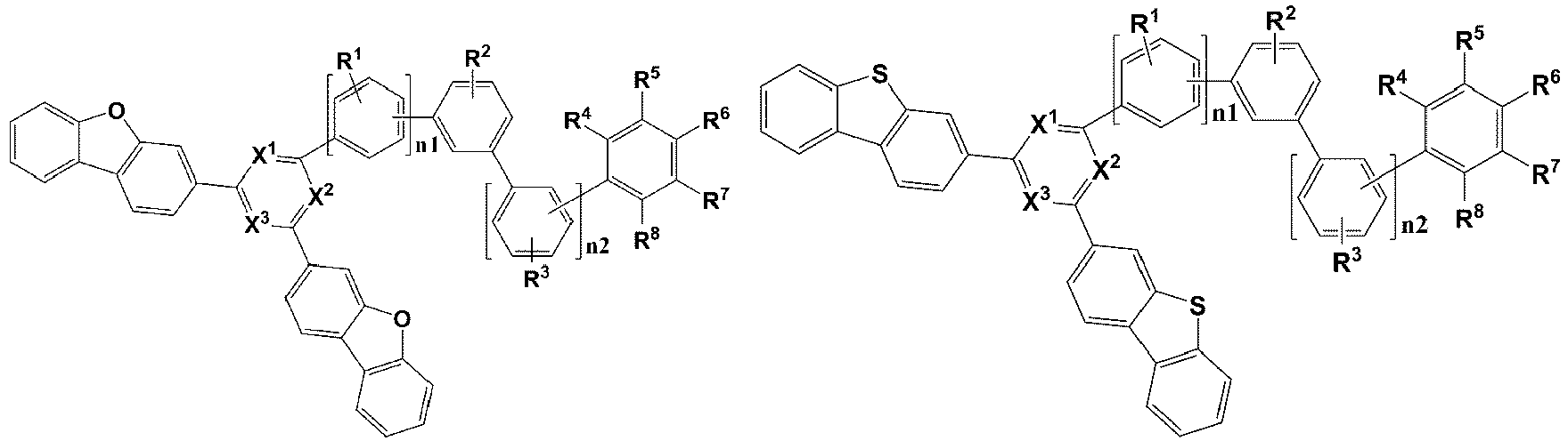

- In Chemical Formula 1A, Chemical Formula 1B, and Chemical Formula 1C, n1 and n2, R1 to R8 are the same as above, and
X1 to X3 are independently N or CH provided that at least two of X1 to X3 are N. - As shown in Chemical Formulae 1A to 1C, when the N-containing 6-membered ring includes a substituent directly linked at a position No. 3 of a dibenzofuranyl group and/or a dibenzothiophenyl group without a linking group, an optimal effect in terms of a driving voltage decrease and a life-span increase may be obtained by positioning LUMO phore on one plane and thus maximizing an expansion effect. However, when the dibenzofuran and/or the dibenzothiophene is linked with the N-containing 6-membered ring at not the position No. 3 but the other positions or through an arylene linker and the like therebetween, an effect of the driving voltage decrease through the LUMO expansion and a stability increase through a fusion of rings may be reduced.
- In an example embodiment of the present invention, Chemical Formula 1 may be represented by Chemical Formula 1A, or Chemical Formula 1B, for example Chemical Formula 1A.
- In an example embodiment of the present invention, both of n1 and n2 are 0 or n1=1, n2=0; or n1=0, n2=1, and Chemical Formula 1 has a structure including a meta-bonded arylene and may be for example represented by Chemical Formula 1-1 or Chemical Formula 1-2 and more specifically represented by Chemical Formula 1-1.

- In Chemical Formulae 1-1 to 1-2, X1 to X3, Y1 and Y2, n2, and R1 to R8 are the same as described above.
- Particularly, R2 of Chemical Formulae 1-1 and 1-2 may be a substituted or unsubstituted C1 to C10 alkyl group, a substituted or unsubstituted C6 to C30 aryl group, or a substituted or unsubstituted C2 to C30 heterocyclic group, and more specifically R2 may be substituted in a meta position, which may be represented by Chemical Formula 1-1a or Chemical Formula 1-2a. Herein, R2-substituted phenylene may include a kinked terphenyl group.


- In an example embodiment of the present invention, R2 may be a substituted or unsubstituted C1 to C4 alkyl group or a substituted or unsubstituted C6 to C30 aryl group, for example, a phenyl group, a biphenyl group, a terphenyl group, or a naphthyl group, and more specifically a substituted or unsubstituted phenyl group.
- When the kinked terphenyl group is included, a glass transition temperature (Tg) may be increased effectively, and a low molecular weight compound having a high glass transition temperature (Tg) may be designed and thereby thermal characteristics may be ensured and stability and the like may be ensured.
- The glass transition temperature (Tg) may have a relation with thermal stability of a compound and a device including the same. That is, when a compound for an organic optoelectronic device having a high glass transition temperature (Tg) is applied to an organic light emitting diode in a form of a thin film, degradation by temperature may be prevented and an organic compound and life-span characteristics of a device may be ensured in subsequent processes after deposition of the compound for an organic optoelectronic device.
- In Chemical Formulae 1-1 and 1-2, a linking group represented by

- The compound for an organic optoelectronic device represented by Chemical Formula 1 may be for example selected from compounds of Group 1, but is not limited thereto.


- The first compound for an organic optoelectronic device may be applied to an organic optoelectronic device alone or with other compounds for an organic optoelectronic device. When the compound for an organic optoelectronic device is used with other compounds for an organic optoelectronic device, they may be applied in a form of a composition.
- Hereinafter, one example of a composition for an organic optoelectronic device including the first compound for an organic optoelectronic device is described.
- A composition for an organic optoelectronic device according to another embodiment of the present invention includes the first compound for an organic optoelectronic device; and a second compound for an organic optoelectronic device represented by Chemical Formula 2.


- In Chemical Formula 2,
L1 and L2 are independently a single bond, a substituted or unsubstituted C6 to C30 arylene group, a substituted or unsubstituted C2 to C30 heteroarylene group, or a combination thereof,
Ar1 and Ar2 are independently a substituted or unsubstituted C6 to C30 aryl group, a substituted or unsubstituted C2 to C30 heterocyclic group, or a combination thereof,
R9 to R14 are independently hydrogen, deuterium, a substituted or unsubstituted C1 to C20 alkyl group, a substituted or unsubstituted C6 to C30 aryl group, a substituted or unsubstituted C2 to C30 heterocyclic group, or a combination thereof, and
m is an integer of 0 to 2;
wherein the "substituted" refers to replacement of at least one hydrogen by deuterium, a C1 to C4 alkyl group, a C6 to C18 aryl group, or a C2 to C30 heteroaryl group. - In an example embodiment of the present invention, L1 and L2 of Chemical Formula 2 may independently be a single bond, or a substituted or unsubstituted C6 to C18 arylene group.
- In an example embodiment of the present invention, Ar1 and Ar2 of Chemical Formula 2 may independently be a substituted or unsubstituted phenyl group, a substituted or unsubstituted biphenyl group, a substituted or unsubstituted terphenyl group, a substituted or unsubstituted naphthyl group, a substituted or unsubstituted anthracenyl group, a substituted or unsubstituted triphenylenyl group, a substituted or unsubstituted pyridinyl group, a substituted or unsubstituted pyrimidinyl group, a substituted or unsubstituted quinazolyl group, a substituted or unsubstituted isoquinazolyl group, a substituted or unsubstituted dibenzothiophenyl group, a substituted or unsubstituted dibenzofuranyl group, a substituted or unsubstituted triazinyl group, a substituted or unsubstituted quinolinyl group, a substituted or unsubstituted isoquinolinyl group, a substituted or unsubstituted carbazolyl group, a substituted or unsubstituted fluorenyl group, or a combination thereof.
- In an example embodiment of the present invention, Ar1 and Ar2 of Chemical Formula 2 may independently be a substituted or unsubstituted phenyl group, a substituted or unsubstituted biphenyl group, a substituted or unsubstituted terphenyl group, a substituted or unsubstituted naphthyl group, a substituted or unsubstituted anthracenyl group, a substituted or unsubstituted triphenylenyl group, a substituted or unsubstituted pyridinyl group, a substituted or unsubstituted quinazolyl group, a substituted or unsubstituted isoquinazolyl group, a substituted or unsubstituted dibenzothiophenyl group, a substituted or unsubstituted dibenzofuranyl group, a substituted or unsubstituted quinolinyl group, a substituted or unsubstituted isoquinolinyl group, a substituted or unsubstituted carbazolyl group, a substituted or unsubstituted fluorenyl group, or a combination thereof.
- In an example embodiment of the present invention, R9 to R14 of Chemical Formula 2 may independently be hydrogen, deuterium, or a substituted or unsubstituted C6 to C12 aryl group.
- In an example embodiment of the present invention, m of Chemical Formula 2 may be 0 or 1.
- In a specific example embodiment of the present invention, Chemical Formula 2 may be one of structures of Group II and *-L1-Ar1 and *-L2-Ar2 may be one of substituents of Group III.


- In Groups II and III, * is a linking point.
- The second compound for an organic optoelectronic device represented by Chemical Formula 2 may be for example selected from compounds of Group 2.


- The first host compound and the second host compound may variously be combined to provide various compositions.
- A composition according to an example embodiment of the present invention includes a compound represented by Chemical Formula 1-I or Chemical Formula 1-II as a first host, and a compound represented by Chemical Formula C-8 or Chemical Formula C-17 of Group II as a second host.
- In addition, a first host represented by Chemical Formula 1-A, or Chemical Formula 1-B and a second host represented by Chemical Formula C-8 or Chemical Formula C-17 of Group II may be included.
- A first host represented by Chemical Formula 1-1 and a second host represented by Chemical Formula C-8 or Chemical Formula C-17 of Group II may be included.
- For example, *-L1-Ar1 and *-L2-Ar2 of Chemical Formula 2 may be selected from B-1, B-2, B-3, and B-16 of Group III.
- The second compound for an organic optoelectronic device is used with the first compound for an organic optoelectronic device in a light-emitting layer, and thereby charge mobility and stability are increased and luminous efficiency and life-span characteristics are improved. In addition, a ratio between the second compound for an organic optoelectronic device and the first compound for an organic optoelectronic device is controlled and thereby charge mobility may be controlled.
- For example, the first compound for an organic optoelectronic device and the second compound for an organic optoelectronic device may be included in a weight ratio of about 1:9 to 9:1, specifically 2:8 to 8:2, 3:7 to 7:3, 4:6 to 6:4, or 5:5, and for example the first compound for an organic optoelectronic device and the second compound for an organic optoelectronic device may be included in a weight ratio of 3:7. Within the ranges, efficiency and life-span may be improved simultaneously.
- The composition may further include one or more organic compound in addition to the first compound for an organic optoelectronic device and the second compound for an organic optoelectronic device.
- The compound for an organic optoelectronic device may further include a dopant. The dopant may be a red, green, or blue dopant.
- The dopant is a material in small amount to cause light emission and may be generally a material such as a metal complex that emits light by multiple excitation into a triplet or more. The dopant may be for example an inorganic, organic, or organic/inorganic compound, and one or more kinds thereof may be used.
- One example of the dopant may be a phosphorescent dopant and examples of the phosphorescent dopant may be an organometal compound including Ir, Pt, Os, Ti, Zr, Hf, Eu, Tb, Tm, Fe, Co, Ni, Ru, Rh, Pd, or a combination thereof. The phosphorescent dopant may be, for example a compound represented by Chemical Formula Z, but is not limited thereto.
[Chemical Formula Z] L2MX
- In Chemical Formula Z, M is a metal, and L and X are the same or different, and are a ligand to form a complex compound with M.
- The M may be for example, Ir, Pt, Os, Ti, Zr, Hf, Eu, Tb, Tm, Fe, Co, Ni, Ru, Rh, Pd, or a combination thereof and L and X may be for example a bidendate ligand.
- Hereinafter, an organic optoelectronic device including the compound for an organic optoelectronic device or the composition for an organic optoelectronic device is described.
- An organic optoelectronic device according to another embodiment includes an anode and a cathode facing each other and at least one organic layer disposed between the anode and the cathode, wherein the organic layer includes the compound for an organic optoelectronic device or the composition for an organic optoelectronic device.
- For example, the organic layer may include a light-emitting layer and the light-emitting layer may include the compound for an organic optoelectronic device or the composition for an organic optoelectronic device.
- Specifically, the compound for an organic optoelectronic device or the composition for an organic optoelectronic device may be included as a green host of the light-emitting layer.
- In addition, the organic layer includes a light-emitting layer and at least one auxiliary layer selected from a hole injection layer, a hole transport layer, an electron blocking layer, an electron transport layer, an electron injection layer, and a hole blocking layer and the auxiliary layer may include the compound for an organic optoelectronic device or the composition for an organic optoelectronic device.
- The auxiliary layer may further include an electron transport auxiliary layer that is adjacent to the light-emitting layer and the electron transport auxiliary layer may include the compound for an organic optoelectronic device, or the composition for an organic optoelectronic device.
- In an example embodiment of the present invention, the compound for an organic optoelectronic device in the electron transport auxiliary layer may be represented by Chemical Formula 1-I, Chemical Formula 1A, or Chemical Formula 1-1.
- The organic optoelectronic device may be any device to convert electrical energy into photoenergy and vice versa without particular limitation, and may be, for example an organic photoelectric diode, an organic light emitting diode, an organic solar cell, and an organic photo conductor drum.
- Herein, an organic light emitting diode as one example of an organic optoelectronic device is described referring to drawings.
-
FIGS. 1 and 2 are cross-sectional views showing organic light emitting diodes according to embodiments. - Referring to
FIG. 1 , an organiclight emitting diode 100 according to an embodiment includes ananode 120 and acathode 110 facing each other and anorganic layer 105 between theanode 120 and thecathode 110. - The
anode 120 may be made of a conductor having a large work function to help hole injection, and may be for example a metal, a metal oxide and/or a conductive polymer. Theanode 120 may be, for example a metal nickel, platinum, vanadium, chromium, copper, zinc, gold, and the like or an alloy thereof; metal oxide such as zinc oxide, indium oxide, indium tin oxide (ITO), indium zinc oxide (IZO), and the like; a combination of metal and oxide such as ZnO and Al or SnO2 and Sb; a conductive polymer such as poly(3-methylthiophene), poly(3,4-(ethylene-1,2-dioxy)thiophene) (PEDT), polypyrrole, and polyaniline, but is not limited thereto. - The
cathode 110 may be made of a conductor having a small work function to help electron injection, and may be for example a metal, a metal oxide and/or a conductive polymer. Thecathode 110 may be for example a metal or an alloy thereof such as magnesium, calcium, sodium, potassium, titanium, indium, yttrium, lithium, gadolinium, aluminum, silver, tin, lead, cesium, barium, and the like; a multi-layer structure material such as LiF/Al, LiO2/Al, LiF/Ca, LiF/Al and BaF2/Ca, but is not limited thereto. - The
organic layer 105 includes a light-emittinglayer 130 including the compound for an organic optoelectronic device. -
FIG. 2 is a cross-sectional view of an organic light emitting diode according to another embodiment. - Referring to
FIG. 2 , an organiclight emitting diode 200 further includes a holeauxiliary layer 140 in addition to the light-emittinglayer 130. The holeauxiliary layer 140 may further increase hole injection and/or hole mobility and block electrons between theanode 120 and the light-emittinglayer 130. The holeauxiliary layer 140 may be, for example a hole transport layer, a hole injection layer, and/or an electron blocking layer, and may include at least one layer. - The
organic layer 105 ofFIG. 1 or 2 may further include an electron injection layer, an electron transport layer, an electron transport auxiliary layer, a hole transport layer, a hole transport auxiliary layer, a hole injection layer, or a combination thereof even if they are not shown. The compound for an organic optoelectronic device of the present invention may be included in these organic layers. The organiclight emitting diodes - The organic light emitting diode may be applied to an organic light emitting diode display.
- Hereinafter, the embodiments are illustrated in more detail with reference to examples. These examples, however, are not in any sense to be interpreted as limiting the scope of the invention.
- Hereinafter, starting materials and reactants used in Examples and Synthesis Examples were purchased from Sigma-Aldrich Co., Ltd. or TCI Inc. as far as there is no particular comment or were synthesized by known methods.
- The compound as one specific examples of the present invention was synthesized through the following steps.
-

- Cyanuric chloride (15 g, 81.34 mmol) was dissolved in anhydrous tetrahydrofuran (200 mL) in a 500 mL round-bottomed flask, 1 equivalent of a 3-biphenyl magnesium bromide solution (0.5 M tetrahydrofuran) was added thereto in a dropwise fashion at 0° C under a nitrogen atmosphere, and the temperature was slowly increased up to room temperature. A reaction solution was stirred at room temperature for 1 hour and then, added to ice water (500 mL) to separate layers. An organic layer was separated therefrom, treated with anhydrous magnesium sulfate, and concentrated. Concentrated residue was recrystallized with tetrahydrofuran and methanol to obtain Intermediate A-1-1 (17.2 g).
- Intermediate A-1-1 (17.2 g, 56.9 mmol) was added to tetrahydrofuran (200 mL) and distilled water (100 mL) in a 500 mL round-bottomed flask, 2 equivalents of dibenzofuran-3-boronic acid (cas: 395087-89-5), 0.03 equivalents of tetrakistriphenylphosphine palladium, and 2 equivalents of potassium carbonate were added thereto, and the mixture was heated and refluxed under a nitrogen atmosphere. After 18 hours, a reaction solution was cooled down, and a solid precipitated therein was filtered and washed with water (500 mL). The solid was recrystallized with monochlorobenzene (500 mL) to obtain Compound A-1 (12.87 g).
LC/MS calculated for: C39H23N3O2 Exact Mass: 565.1790 found for: 566.18 [M+H] -

- Magnesium (7.86 g, 323 mmol) and iodine (1.64 g, 6.46 mmol) were added to tetrahydrofuran (THF, 0.1 L) under a nitrogen environment and mixed therewith for 30 minutes, and 3-bromo-m-terphenyl (100 g, 323 mmol) dissolved in THF (0.3 L) was slowly added thereto in a dropwise fashion at 0 ° C for 30 minutes. This mixed solution was slowly added in a dropwise fashion to cyanuric chloride (64.5 g, 350 mmol) dissolved in THF (0.5 L) at 0 °C over 30 minutes. After the reaction was complete, water was added to the reaction solution, the mixture was extracted with dichloromethane (DCM) and treated with anhydrous MgSO4 to remove moisture, and the resultant was filtered and concentrated under a reduced pressure. The obtained residue was separated and purified through flash column chromatography to obtain Intermediate A-2-1 (85.5 g, 70 %).
- Compound A-2 was synthesized according to the same method as b) of Synthesis Example 1 by using Intermediate A-2-1.
LC/MS calculated for: C45H27N3O2 Exact Mass: 641.2103 found for 642.21 [M+H] -

- Magnesium (7.86 g, 323 mmol) and iodine (1.64 g, 6.46 mmol) were added to tetrahydrofuran (THF, 0.1 L) and stirred therewith for 30 minutes under a nitrogen environment, and 1-bromo-3,5-diphenylbenzene (100 g, 323 mmol) dissolved in THF (0.3 L) was slowly added thereto in a dropwise fashion at 0 °C for 30 minutes. This mixed solution was slowly added in a dropwise fashion to cyanuric chloride (64.5 g, 350 mmol) dissolved in THF (0.5 L) at 0° C for 30 minutes. After the reaction was complete, water was added to the reaction solution, the mixture was extracted with dichloromethane (DCM) and treated with anhydrous MgSO4 to remove moisture, and the resultant was filtered and concentrated under a reduced pressure. The obtained residue was separated and purified through flash column chromatography to obtain Intermediate A-5-1 (79.4 g, 65 %).
- Compound A-5 was synthesized according to the same method as b) of Synthesis Example 1 by using Intermediate A-5-1.
LC/MS calculated for: C45H27N3O2 Exact Mass: 641.2103 found for 642.21 [M+H] -

- Compound A-6 was synthesized according to the same method as b) of Synthesis Example 1 by using dibenzothiophene-3-boronic acid (Cas No.: 108847-24-1) instead of Intermediate A-1-1 and dibenzofuran-3-boronic acid (Cas No.: 395087-89-5).
LC/MS calculated for: C39H23N3S2 Exact Mass: 597.1333 found for 598.13 [M+H] -

- 2,4,6-trichloropyrimidine (18.3 g, 100 mmol) was added to tetrahydrofuran (200 mL) and distilled water (100 mL) in a 500 mL round-bottomed flask, 1.9 equivalents of dibenzofuran-3-boronic acid (Cas No.: 395087-89-5), 0.03 equivalents of tetrakistriphenylphosphine palladium, and 2 equivalents of potassium carbonate were added thereto, and the mixture was heated and refluxed under a nitrogen atmosphere. After 18 hours, the reaction solution was cooled down, and a solid precipitated therein was filtered and washed with water (500 mL). The solid was recrystallized with monochlorobenzene (500 mL) to obtain Intermediate A-15-1 (26.8 g, a yield of 60 %).
- Compound A-15 was synthesized according to the same method as b) of Synthesis Example 1 by using Intermediate A-15-1 and 1.1 equivalents of 3,5-diphenylbenzene boronic acid.
LC/MS calculated for: C46H28N2O2 Exact Mass: 640.2151 found for 641.21 [M+H] -

- Intermediate A-21-1 was synthesized according to the same method as a) of Synthesis Example 5 by using the dibenzothiophene-3-boronic acid (Cas No. 108847-24-1) instead of the dibenzofuran-3-boronic acid (cas: 395087-89-5).
- Compound A-21 was synthesized according to the same method as b) of Synthesis Example 5 by using Intermediate A-21-1 and 1.1 equivalents of biphenyl-3-boronic acid.
LC/MS calculated for: C40H24N2S2 Exact Mass: 596.1381 found for 597.14 [M+H] -


- 3-bromo-6-phenyl-N-metabiphenylcarbazole (20.00 g, 42.16 mmol) and N-phenylcarbazole-3-boronic ester (17.12 g, 46.38 mmol) were mixed with a mixture of tetrahydrofuran:toluene (1:1, 175 mL) and a 2 M-potassium carbonate aqueous solution (75 mL) under a nitrogen atmosphere in a 500 mL round-bottomed flask equipped with an agitator, tetrakistriphenylphosphinepalladium (0) (1.46 g, 1.26 mmol) was added thereto, and the obtained mixture was heated and refluxed under a nitrogen flow for 12 hours. When the reaction was complete, the reactant was poured into methanol, and a solid produced therein was filtered, sufficiently washed with water and methanol, and dried. The resulting material was dissolved in chlorobenzene (700 mL) through heating, the solution was silica gel-filtered, and after completely removing a solvent therefrom, a solid obtained therefrom was dissolved in chlorobenzene (400 mL) through heating and recrystallized to obtain Compound E-130 (18.52 g, a yield of 69 %).
calcd. C42H32N2: C, 90.54; H, 5.07; N, 4.40; found: C, 90.54; H, 5.07; N, 4.40 -


- N-phenyl-3,3-bicarbazole (6.3 g, 15.4 mmol), 4-(4-bromophenyl)dibenzo[b,d]furan (5.0 g, 15.4 mmol), sodium t-butoxide (3.0 g, 30.7 mmol), tris(dibenzylideneacetone)dipalladium (0.9 g, 1.5 mmol), and tri t-butylphosphine (1.2 mL, 50 % in toluene) were mixed with xylene (100 mL) in a 250 mL round flask, and the mixture was heated and refluxed under a nitrogen flow for 15 hours. The obtained mixture was added to methanol (300 mL), and a solid crystallized therein was dissolved in dichlorobenzene, filtered with silica gel/Celite, and after removing an appropriate amount of an organic solvent, recrystallized with methanol to obtain Compound E-137 (7.3 g, a yield of 73 %).
calcd. C48H30N2O: C, 88.59; H, 4.65; N, 4.30; O, 2.46; found: C, 88.56; H, 4.62; N, 4.20; O, 2.43 -


- Comparative Compound 1 was synthesized according to the same method as b) of Synthesis Example 1 by using 2-chloro-4,6-diphenyltriazine and dibenzothiophene-3-boronic acid.
LC/MS calculated for: C27H17N3S Exact Mass: 415.1143 found for 416.11 [M+H] -

- Comparative Compound 2 was synthesized according to the same method as b) of Synthesis Example 1 by using 2,4-bis([1,1'-biphenyl]-4-yl)-6-chloro-1,3,5-triazine and dibenzothiophene-3-boronic acid.
LC/MS calculated for: C39H25N3S Exact Mass: 567.1769 found for 568.18 [M+H] -

- Comparative Compound 3 was synthesized according to the same method as b) of Synthesis Example 1 by using Intermediate A-1-1 and dibenzofuran-2-boronic acid.
LC/MS calculated for: C39H23N3O Exact Mass: 565.1790 found for 566.18 [M+H] -


- Comparative Compound 4 was synthesized according to the same method as b) of Synthesis Example 1 by using 2,4-dichloro-6-phenyl-1,3,5-triazine and dibenzofuran-2-yl-3-phenylboronic acid.
LC/MS calculated for: C39H23N3O Exact Mass: 565.1790 found for 566.18 [M+H] -

- Intermediate 5-1 was synthesized according to the same method as b) of Synthesis Example 1 by using 1-bromo-4-chlorobenzene and dibenzofuran-3-boronic acid.
- Intermediate 5-1 (328 mmol) was dissolved in dimethylforamide (DMF, 1.0 L), bis(pinacolato)diboron (100 g, 394 mmol), (1,1'-bis(diphenylphosphine)ferrocene)dichloropalladium (II) (2.68 g, 3.28 mmol), and potassium acetate (96.6 g, 984 mmol) were added thereto, and the mixture was heated and refluxed at 150 ° C for 20 hours. After the reaction was complete, water was added to the reaction solution and the mixture was filtered and dried in a vacuum oven. The obtained residue was separated and purified through flash column chromatography to obtain Intermediate 5-2 (71 %).
- Comparative Compound 5 was synthesized according to the same method as b) of Synthesis Example 1 by using Intermediate 5-2 and 4,6-dichloro-2-phenyl-1,3-pyrimidine.
LC/MS calculated for: C46H28N2O2 Exact Mass: 640.2151 found for 641.22 [M+H] - A glass substrate coated with ITO (indium tin oxide) as a 1500 Å-thick thin film was washed with distilled water. After washed with distilled water, the glass substrate was ultrasonic wave-washed with a solvent such as isopropyl alcohol, acetone, methanol, and the like and dried, moved to a plasma cleaner, cleaned with oxygen plasma for 10 minutes, and moved to a vacuum depositor. This obtained ITO transparent electrode was used as an anode, Compound A was vacuum-deposited on the ITO substrate to form a 700 Å-thick hole injection layer, Compound B was deposited to be 50 Å thick on the injection layer, and Compound C was deposited to be 1020 Å thick to form a hole transport layer. A 400 Å-thick light-emitting layer was formed on the hole transport layer by vacuum-depositing Compound A-1 of Synthesis Example 1 and Compound E-130 of Synthesis Example 7 simultaneously as a host and 10 wt% of tris(2-phenylpyridine)iridium(III) [Ir(ppy)3] as a dopant. Herein, Compound A-1 and Compound E-130 were used at a weight ratio of 3:7 and in the following examples, a ratio is separately described. Subsequently, Compound D and Liq were vacuum-deposited simultaneously at a 1:1 ratio on the light-emitting layer to form a 300 Å-thick electron transport layer and a cathode was formed by sequentially vacuum-depositing Liq to be 15 Å thick and Al to be 1200 Å thick on the electron transport layer, manufacturing an organic light emitting diode.
- The organic light emitting diode had a five-layered organic thin layer, and specifically
ITO/Compound A (700 Å)/Compound B (50 Å)/Compound C (1020 Å)/EML [Compound A-1:E-130:Ir(ppy)3 = 27 wt%:63 wt%:10 wt%] (400 Å)/Compound D:Liq (300 Å)/Liq (15 Å)/Al (1200 Å). - Compound A: N4,N4'-diphenyl-N4,N4'-bis(9-phenyl-9H-carbazol-3-yl)biphenyl-4,4'-diamine
- Compound B: 1,4,5,8,9,11-hexaazatriphenylene-hexacarbonitrile (HAT-CN),
- Compound C: N-(biphenyl-4-yl)-9,9-dimethyl-N-(4-(9-phenyl-9H-carbazol-3-yl)phenyl)-9H-fluoren-2-amine
- Compound D: 8-(4-(4,6-di(naphthalen-2-yl)-1,3,5-triazin-2-yl)phenyl)quinoline
- An organic light emitting diode according to Example 2 was manufactured according to the same method as Example 1 by using Compound A-2 alone.
- Organic light emitting diodes according to Examples 3 to 10 were manufactured according to the same method as Example 1 by using first and second hosts of the present invention as shown in Tables 2 and 3.
- Organic light emitting diodes according to Comparative Examples 1 and 2 were manufactured according to the same method as Example 1 by using Comparative Compound 1 and Comparative Compound 2 respectively alone.
- Organic light emitting diodes according to Comparative Examples 3 to 7 were manufactured according to the same method as Example 1 by using either one of Comparative Compound 1 to Comparative Compound 5 with Compound E-31 with a ratio of 3:7 as shown in Tables 2 and 3.
- Luminous efficiency and life-span characteristics of each organic light emitting diode according to Examples 1 to 10 and Comparative Examples 1 to 7 were measured. Specific measurement methods are as follows, and the results are shown in Table 1.
- The obtained organic light emitting diodes were measured regarding a current value flowing in the unit device, while increasing the voltage from 0 V to 10 V using a current-voltage meter (Keithley 2400), and, the measured current value was divided by area to provide the results.
- Luminance was measured by using a luminance meter (Minolta Cs-1000A), while the voltage of the organic light emitting diodes was increased from 0 V to 10 V.
- Current efficiency (cd/A) at the same current density (10 mA/cm2) were calculated by using the luminance, current density, and voltages (V) from the items (1) and (2).
- T90 life-spans of the organic light emitting diodes according to Examples 1 to 10 and Comparative Examples 1 to 7 were measured as a time when their luminance decreased down to 90 % relative to the initial luminance (cd/m2) after emitting light with 5000 cd/m2 as the initial luminance (cd/m2) and measuring their luminance decreases depending on a time with a Polanonix life-span measurement system.
[Table 1] Single Host Device First host Color Efficiency (Cd/A) Life-span (T90) Example 2 Compound A-2 green 39 140 Comparative Example 1 Comparative Compound 1 green 32 60 Comparative Example 2 Comparative Compound 2 green 33 40 - Referring to Table 1, comparing Examples and Comparative Examples 1 and 2 in case of using a single host, Examples having a structural feature of additionally including a meta-substituted aryl group showed greater than or equal to 1.2 times higher efficiency and at most greater than or equal to 4 times longer life-span than Comparative Examples despite dibenzofuran linked with triazine at the same position No. 3.
[Table 2] Mixed Host Device Effect: Triazine First host Second host First host + Second host ratio Color Effici ency Cd/A Life-span (T90) Example 1 Compound A-1 Compound E-130 3:7 green 51 460 Example 3 Compound A-2 Compound E-130 3:7 green 52 530 Example 4 Compound A-2 Compound E-99 3:7 green 50 600 Example 5 Compound A-2 Compound E-31 3:7 green 51 650 Example 6 Compound A-2 Compound E-137 3:7 green 50 570 Example 7 Compound A-5 Compound E-31 3:7 green 51 600 Example 8 Compound A-6 Compound E-31 3:7 green 49 480 Comparative Example 3 Comparative Compound 1 Compound E-31 3:7 green 48 160 Comparative Example 4 Comparative Compound 2 Compound E-31 3:7 green 46 240 Comparative Example 5 Comparative Compound 3 Compound E-31 3:7 green 46 130 Comparative Example 6 Comparative Compound 4 Compound E-31 3:7 green 50 290 [Table 3] Mixed Host Device Effect: Pyrimidine First host Second host First host + Second host ratio Color Effici ency Cd/A Life-span (T90) Example 9 Compound A-15 Compound E-31 3:7 green 52 340 Example 10 Compound A-21 Compound E-31 3:7 green 53 380 Comparative Example 7 Comparative Compound 5 Compound E-31 3:7 green 46 150 - Referring to Tables 2 and 3, Examples using first and second hosts according to the present invention and having a structural feature of having dibenzofuran linked with triazine at the position No. 3 and/or additionally including a meta-substituted aryl group showed at most 5 times longer life-span than Comparative Example using a mixed host with the same second host.
- This life-span increase effect was equally obtained in the pyrimidine core as well as the triazine core. Accordingly, referring to corresponding device data, a life-span of a corresponding material in a device turned out to be improved through effects of a LUMO expansion and a cyclic fusion, when dibenzofuran or dibenzothiophene is directly linked with an ET core group.
- A driving voltage of each device was measured at 15 mA/cm2 by using a current-voltage meter (Keithley 2400), and the results are shown in Table 4.
[Table 4] First host Second host First host + Second host ratio Color Vd Example 4 Compound A-2 Compound E-99 3:7 green 3.75 Example 5 Compound A-2 Compound E-31 3:7 green 3.90 Example 8 Compound A-6 Compound E-31 3:7 green 3.85 Comparative Example 5 Comparative Compound 3 Compound E-137 3:7 green 4.20 Comparative Example 6 Comparative Compound 4 Compound E-137 3:7 green 4.40 - Referring to Table 4, comparing Examples 4, 5, and 8 using a host combination according to the present invention with Comparative Examples 5 and 6, an excellent effect in terms of a driving voltage was obtained, when the position No. 3 of dibenzofuran or dibenzothiophene is directly substituted and liked with triazine compared with when other positions of dibenzofuran or dibenzothiophene were substituted and linked with triazine even though the aryl linker at a meta position was included and when the dibenzofuran or dibenzothiophene was substituted not directly but through the aryl linker and linked with triazine. Accordingly, the direct substitution of the position No. 3 of the dibenzofuran or dibenzothiophene turned out to bring about an excellent effect in terms of driving.
- ITO (indium tin oxide) was coated to be 1500 Å thick on a glass substrate, and the coated glass substrate was ultrasonic wave-washed with a distilled water. After the washing with distilled water, the glass substrate was ultrasonic wave-washed with a solvent such as isopropyl alcohol, acetone, methanol, and the like and dried, moved to a plasma cleaner, cleaned with oxygen plasma for 10 minutes, and moved to a vacuum depositor. This obtained ITO transparent electrode was used as an anode, a 700 Å-thick hole injection layer was formed on the ITO substrate by vacuum-depositing Compound A, and a hole transport layer was formed on the injection layer by depositing Compound B to be 50 Å thick and Compound C to be 1020 Å thick. Then, a 200 Å-thick light-emitting layer was formed thereon by vacuum-depositing BH113 and BD370 (Manufacturer: SFC Inc.) as a blue fluorescent luminescent host and a dopant in a dopant concentration of 5 wt%. On the light-emitting layer, Compound A-5 was vacuum-deposited to form a 50 Å-thick electron transport auxiliary layer. The electron transport auxiliary layer may be formed by using a material represented by Chemical Formula I alone or mixing the material with the compound of Group E. On the electron transport auxiliary layer, a 300 Å-thick electron transport layer was formed by vacuum-depositing Compound D and Liq simultaneously in a weight ratio of 1:1, and on the electron transport layer, a cathode was formed by sequentially vacuum-depositing Liq to be 15 Å thick and Al to be 1200 Å thick, manufacturing an organic light emitting diode. The organic light emitting diode had a structure of 5 organic thin film layers and specifically, ITO/Compound A (700 Å)/Compound B (50 Å)/ Compound C (1020 Å)/EML[BH113:BD370 = 95:5 (wt:wt)] (200 Å)/Compound A-5 (50 Å)/ Compound D:Liq (300 Å) = 1:1/Liq (15 Å)/Al (1200 Å).
- Compound A: N4,N4'-diphenyl-N4,N4'-bis(9-phenyl-9H-carbazol-3-yl)biphenyl-4,4'-diamine
- Compound B: 1,4,5,8,9,11-hexaazatriphenylene-hexacarbonitrile (HAT-CN),
- Compound C: N-(biphenyl-4-yl)-9,9-dimethyl-N-(4-(9-phenyl-9H-carbazol-3-yl)phenyl)-9H-fluoren-2-amine
- Compound D: 8-(4-(4,6-di(naphthalen-2-yl)-1,3,5-triazin-2-yl)phenyl)quinoline
- An organic light emitting diode was manufactured according to the same method as Example 11 except for using Compound A-15.
- An organic light emitting diode was manufactured according to the same method as Example 11 except for using Comparative Compound 1.
- Current density change, luminance change, and luminous efficiency depending on a voltage of each organic light emitting diode according to Examples 11 and 12 and Comparative Example 8 were measured.
- Specific measurement methods are the same as in Evaluation 1, a method of measuring life-span is as follows, and the results are shown in Table 5.
- T97 life-spans of the organic light emitting diodes according to Example 11, Example 12, and Comparative Example 8 were measured as a time when their luminance decreased down to 97 % relative to the initial luminance (cd/m2) after emitting light with 750 cd/m2 as the initial luminance (cd/m2) and measuring their luminance decrease depending on a time with a Polanonix life-span measurement system.
[Table 5] Devices Electron transport auxiliary layer (weight ratio) Luminous efficiency (cd/A) Color coordinate (x, y) T97(h) @750nit Example 11 compound A-5 6.7 (0.132, 0.149) 85 Example 12 compound A-15 7.1 (0.133, 0.148) 70 Comparative Example 8 Comparative Compound 1 5.9 (0.132, 0.149) 48 - Referring to Table 5, the organic light emitting diodes according to Examples 11 and 12 showed simultaneously improved luminous efficiency and life-span characteristics compared with the organic light emitting diode according to Comparative Example 8.
- While this invention has been described in connection with what is presently considered to be practical example embodiments, it is to be understood that the invention is not limited to the disclosed embodiments, but, on the contrary, is intended to cover various modifications and equivalent arrangements included within the spirit and scope of the appended claims. Therefore, the aforementioned embodiments should be understood to be exemplary but not limiting the present invention in any way.
Claims (15)
- A compound represented by Chemical Formula 1 for an organic optoelectronic device:
 X1 to X3 are independently N or CRa,at least two of X1 to X3 are N,Y1 and Y2 are independently O or S,n1 and n2 are independently an integer of 0 or 1,Ra and R1 to R8 are independently hydrogen, deuterium, a cyano group, a nitro group, a substituted or unsubstituted C1 to C10 alkyl group, a substituted or unsubstituted C6 to C30 aryl group, a substituted or unsubstituted C2 to C30 heterocyclic group, or a combination thereof, andthe "substituted" refers to replacement of at least one hydrogen by deuterium, a C1 to C20 alkyl group, a C6 to C30 aryl group, or a C2 to C30 heteroaryl group.
 - The compound for an organic optoelectronic device of claim 1, wherein the compound is represented by Chemical Formula 1-I, Chemical Formula 1-II, or Chemical Formula 1-III:

 Y1 and Y2 are independently O or S,n1 and n2 are independently an integer of 0 or 1, andR1 to R8 are independently hydrogen, deuterium, a cyano group, a nitro group, a substituted or unsubstituted C1 to C10 alkyl group, a substituted or unsubstituted C6 to C30 aryl group, a substituted or unsubstituted C2 to C30 heterocyclic group, or a combination thereof.
 - The compound for an organic optoelectronic device of claim 1, wherein the compound is represented by Chemical Formula 1A, Chemical Formula 1B, or Chemical Formula 1C:


 X1 to X3 are independently N or CH,at least two of X1 to X3 are N,n1 and n2 are independently an integer of 0 or 1, andR1 to R8 are independently hydrogen, deuterium, a cyano group, a nitro group, a substituted or unsubstituted C1 to C10 alkyl group, a substituted or unsubstituted C6 to C30 aryl group, a substituted or unsubstituted C2 to C30 heterocyclic group, or a combination thereof.
 - The compound for an organic optoelectronic device of claim 1, wherein the compound is represented by Chemical Formula 1-1 or 1-2:

 X1 to X3 are independently N or CH,at least two of X1 to X3 are N,Y1 and Y2 are independently O or S,n2 is an integer of 0 or 1, andR1 to R8 are independently hydrogen, deuterium, a cyano group, a nitro group, a substituted or unsubstituted C1 to C10 alkyl group, a substituted or unsubstituted C6 to C30 aryl group, a substituted or unsubstituted C2 to C30 heterocyclic group, or a combination thereof.
 - The compound for an organic optoelectronic device of claim 1, wherein the R1 to R8 are independently hydrogen, a substituted or unsubstituted phenyl group, a substituted or unsubstituted biphenyl group, a substituted or unsubstituted naphthyl group, a substituted or unsubstituted p-terphenyl group, a substituted or unsubstituted m-terphenyl group, a substituted or unsubstituted o-terphenyl group, a substituted or unsubstituted anthracenyl group, a substituted or unsubstituted phenanthrenyl group, a substituted or unsubstituted triphenylenyl group, or a substituted or unsubstituted fluorenyl group.
- The compound for an organic optoelectronic device of claim 1, wherein the compound is selected from compounds of Group 1:


- A composition for an organic optoelectronic device, comprising
the compound for an organic optoelectronic device of claim 1; and
a second compound for an organic optoelectronic device represented by Chemical Formula 2: L1 and L2 are independently a single bond, a substituted or unsubstituted C6 to C30 arylene group, a substituted or unsubstituted C2 to C30 heteroarylene group, or a combination thereof,Ar1 and Ar2 are independently a substituted or unsubstituted C6 to C30 aryl group, a substituted or unsubstituted C2 to C30 heterocyclic group, or a combination thereof,R9 to R14 are independently hydrogen, deuterium, a substituted or unsubstituted C1 to C20 alkyl group, a substituted or unsubstituted C6 to C30 aryl group, a substituted or unsubstituted C2 to C30 heterocyclic group, or a combination thereof, andm is an integer of 0 to 2;wherein the "substituted" refers to replacement of at least one hydrogen by deuterium, a C1 to C4 alkyl group, a C6 to C18 aryl group, or a C2 to C30 heteroaryl group.
 - The composition for an organic optoelectronic device of claim 7, wherein Ar1 and Ar2 of Chemical Formula 2 are independently, a substituted or unsubstituted phenyl group, a substituted or unsubstituted biphenyl group, a substituted or unsubstituted terphenyl group, a substituted or unsubstituted naphthyl group, a substituted or unsubstituted anthracenyl group, a substituted or unsubstituted triphenylenyl group, a substituted or unsubstituted pyridinyl group, a substituted or unsubstituted pyrimidinyl group, a substituted or unsubstituted triazinyl group, a substituted or unsubstituted quinolinyl group, a substituted or unsubstituted isoquinolinyl group, a substituted or unsubstituted quinazolyl group, a substituted or unsubstituted isoquinazolyl group, a substituted or unsubstituted dibenzothiophenyl group, a substituted or unsubstituted dibenzofuranyl group, a substituted or unsubstituted carbazolyl group, a substituted or unsubstituted fluorenyl group, or a combination thereof.
- The composition for an organic optoelectronic device of claim 7, wherein Chemical Formula 2 is one of structures of Group II and
*-L1-Ar1 and *-L2-Ar2 are one of substituents of Group III:


- The composition for an organic optoelectronic device of claim 9, wherein Chemical Formula 2 is represented by Chemical Formula C-8 or Chemical Formula C-17 of Group II and
*-L1-Ar1 and *-L2-Ar2 are selected from B-1, B-2, B-3, and B-16 of Group III. - An organic optoelectronic device, comprising
an anode and a cathode facing each other, and
at least one organic layer disposed between the anode and the cathode,
wherein the organic layer includes the compound for an organic optoelectronic device of any one of claim 1 to claim 6; or
the composition for an organic optoelectronic device of any one of claim 7 to claim 10. - The organic optoelectronic device of claim 11, wherein the organic layer includes a light-emitting layer, and
the light-emitting layer includes the compound for an organic optoelectronic device or the composition for an organic optoelectronic device. - The organic optoelectronic device of claim 12, wherein the compound for an organic optoelectronic device or the composition for an organic optoelectronic device is included as a host of the light-emitting layer.
- The organic optoelectronic device of claim 12, wherein the organic layer further includes at least one auxiliary layer selected from a hole injection layer, a hole transport layer, an electron blocking layer, an electron transport layer, an electron injection layer, and a hole blocking layer,
the auxiliary layer further includes an electron transport auxiliary layer that is adjacent to the light-emitting layer, and
the electron transport auxiliary layer includes the compound for an organic optoelectronic device; or the composition for an organic optoelectronic device. - A display device comprising the organic optoelectronic device of claim 11.
Applications Claiming Priority (2)
| Application Number | Priority Date | Filing Date | Title |
|---|---|---|---|
| KR1020160081767A KR102027961B1 (en) | 2016-06-29 | 2016-06-29 | Compound for organic optoelectronic device, composition for organic optoelectronic device and organic optoelectronic device and display device |
| PCT/KR2017/000619 WO2018004096A1 (en) | 2016-06-29 | 2017-01-18 | Compound for organic optoelectronic device, composition for organic optoelectronic device, organic optoelectronic device and display apparatus |
Publications (3)
| Publication Number | Publication Date |
|---|---|
| EP3480278A1 true EP3480278A1 (en) | 2019-05-08 |
| EP3480278A4 EP3480278A4 (en) | 2020-01-22 |
| EP3480278B1 EP3480278B1 (en) | 2024-05-08 |
Family
ID=60787466
Family Applications (1)
| Application Number | Title | Priority Date | Filing Date |
|---|---|---|---|
| EP17820373.3A Active EP3480278B1 (en) | 2016-06-29 | 2017-01-18 | Compound for organic optoelectronic device, composition for organic optoelectronic device, organic optoelectronic device and display apparatus |
Country Status (7)
| Country | Link |
|---|---|
| US (1) | US11706975B2 (en) |
| EP (1) | EP3480278B1 (en) |
| JP (1) | JP6644920B2 (en) |
| KR (1) | KR102027961B1 (en) |
| CN (1) | CN109415625B (en) |
| TW (1) | TWI637952B (en) |
| WO (1) | WO2018004096A1 (en) |
Cited By (1)
| Publication number | Priority date | Publication date | Assignee | Title |
|---|---|---|---|---|
| EP4033556A4 (en) * | 2019-09-16 | 2023-09-13 | Solus Advanced Materials Co., Ltd. | ORGANIC ELECTROLUMINESCENT DEVICE |
Families Citing this family (34)
| Publication number | Priority date | Publication date | Assignee | Title |
|---|---|---|---|---|
| KR102037816B1 (en) * | 2016-11-16 | 2019-10-29 | 삼성에스디아이 주식회사 | Organic optoelectronic device and display device |
| KR102044943B1 (en) | 2018-05-28 | 2019-11-14 | 삼성에스디아이 주식회사 | Compound, composition and organic optoelectronic device and display device |
| KR102430047B1 (en) * | 2018-06-08 | 2022-08-05 | 삼성에스디아이 주식회사 | Compound for optoelectronic device, composition for optoelectronic device, organic optoelectronic device and display device |
| KR102217250B1 (en) * | 2018-06-12 | 2021-02-18 | 삼성에스디아이 주식회사 | Composition for organic optoelectronic device and organic optoelectronic device and display device |
| KR102283787B1 (en) * | 2018-11-02 | 2021-07-30 | 삼성에스디아이 주식회사 | Organic optoelectronic device and display device |
| CN112533914B (en) | 2018-11-06 | 2025-02-21 | 株式会社Lg化学 | Compound and organic light-emitting device containing the same |
| WO2020096351A1 (en) * | 2018-11-06 | 2020-05-14 | 주식회사 엘지화학 | Novel compound and organic light-emitting element using same |
| KR102448566B1 (en) | 2018-12-04 | 2022-09-27 | 삼성에스디아이 주식회사 | Organic optoelectronic devices and display devices |
| KR102366291B1 (en) | 2019-02-15 | 2022-02-21 | 삼성에스디아이 주식회사 | Composition for optoelectronic device and organic optoelectronic device and display device |
| KR102365130B1 (en) | 2019-02-15 | 2022-02-17 | 삼성에스디아이 주식회사 | Composition for optoelectronic device and organic optoelectronic device and display device |
| KR102624670B1 (en) | 2019-10-29 | 2024-01-11 | 삼성에스디아이 주식회사 | Compound for organic optoelectronic device, composition for organic optoelectronic device and organic optoelectronic device and display device |
| CN112851645B (en) * | 2019-11-28 | 2023-06-23 | 南京高光半导体材料有限公司 | A kind of organic electroluminescent material and organic electroluminescent device based on triazine ring structure |
| KR102739126B1 (en) | 2020-06-10 | 2024-12-05 | 삼성전자주식회사 | Composition and organic light emitting device including the same |
| WO2022047098A1 (en) * | 2020-08-27 | 2022-03-03 | Utica Leaseco, Llc | Bifacial optoelectronic device with transparent conductive layer |
| JP2023542097A (en) * | 2020-09-11 | 2023-10-05 | エルティー・マテリアルズ・カンパニー・リミテッド | Heterocyclic compounds and organic light-emitting devices containing them |
| KR102786596B1 (en) * | 2021-05-18 | 2025-03-26 | 삼성에스디아이 주식회사 | Composition for organic optoelectronic device, organic optoelectronic device and display device |
| KR102756338B1 (en) * | 2021-12-10 | 2025-01-21 | 엘티소재주식회사 | Heterocyclic compound, organic light-emitting device comprising same and composition for organic material layer of organic light-emitting device comprising same |
| EP4631325A1 (en) | 2022-12-08 | 2025-10-15 | Merck Patent GmbH | Organic electronic device and special materials for organic electronic devices |
| KR20250124370A (en) | 2022-12-19 | 2025-08-19 | 메르크 파텐트 게엠베하 | Materials for electronic devices |
| CN120826409A (en) | 2023-03-20 | 2025-10-21 | 默克专利有限公司 | Materials for organic electroluminescent devices |
| KR20260058873A (en) | 2023-08-29 | 2026-04-29 | 메르크 파텐트 게엠베하 | Materials for organic electroluminescent devices |
| CN121753521A (en) | 2023-08-30 | 2026-03-27 | 默克专利有限公司 | Material for organic light emitting device |
| CN121773745A (en) | 2023-08-30 | 2026-03-31 | 默克专利有限公司 | Material for organic light emitting device |
| CN121753522A (en) | 2023-08-30 | 2026-03-27 | 默克专利有限公司 | Material for organic light emitting device |
| CN121969629A (en) | 2023-10-04 | 2026-05-01 | 默克专利有限公司 | Materials for organic electroluminescent devices |
| WO2025104058A1 (en) | 2023-11-16 | 2025-05-22 | Merck Patent Gmbh | Materials for organic electronic devices |
| WO2025119821A1 (en) | 2023-12-05 | 2025-06-12 | Merck Patent Gmbh | Material composition for organic electroluminescent devices |
| WO2025168515A1 (en) | 2024-02-06 | 2025-08-14 | Merck Patent Gmbh | Materials for organic electronic devices |
| WO2025195961A1 (en) | 2024-03-19 | 2025-09-25 | Merck Patent Gmbh | Organic light-emitting devices |
| WO2025228800A1 (en) | 2024-04-30 | 2025-11-06 | Merck Patent Gmbh | Materials for organic electronic devices |
| WO2026017611A1 (en) | 2024-07-15 | 2026-01-22 | Merck Patent Gmbh | Organic light emitting device |
| WO2026017608A1 (en) | 2024-07-15 | 2026-01-22 | Merck Patent Gmbh | Materials for organic light-emitting devices |
| WO2026017607A1 (en) | 2024-07-15 | 2026-01-22 | Merck Patent Gmbh | Organic light-emitting device |
| WO2026017612A1 (en) | 2024-07-15 | 2026-01-22 | Merck Patent Gmbh | Organic light-emitting device |
Family Cites Families (81)
| Publication number | Priority date | Publication date | Assignee | Title |
|---|---|---|---|---|
| US6229012B1 (en) | 1998-10-01 | 2001-05-08 | Xerox Corporation | Triazine compositions |
| US6900458B2 (en) | 2003-02-21 | 2005-05-31 | Universal Display Corporation | Transflective display having an OLED backlight |
| US7306970B2 (en) | 2004-08-30 | 2007-12-11 | International Business Machines Corporation | Method and apparatus for manufacturing an optoelectronic device |
| US7651791B2 (en) | 2005-12-15 | 2010-01-26 | Idemitsu Kosan Co., Ltd. | Material for organic electroluminescence device and electroluminescence device employing the same |
| WO2010044342A1 (en) | 2008-10-15 | 2010-04-22 | コニカミノルタホールディングス株式会社 | Organic el element, organic el element manufacturing method, white organic el element, display device, and illumination device |
| US9617255B2 (en) | 2009-02-06 | 2017-04-11 | Konica Minolta, Inc. | Organic electroluminescent element, and illumination device and display device each comprising the element |
| KR101741415B1 (en) | 2009-04-29 | 2017-05-30 | 롬엔드하스전자재료코리아유한회사 | Novel organic electroluminescent compounds and organic electroluminescent device using the same |
| KR101297158B1 (en) | 2010-02-22 | 2013-08-21 | 제일모직주식회사 | Compound for organic photoelectric device and organic photoelectric device including the same |
| WO2011132683A1 (en) * | 2010-04-20 | 2011-10-27 | 出光興産株式会社 | Bis-carbazole derivative, material for organic electroluminescent element and organic electroluminescent element using same |
| CN102947416B (en) | 2010-06-18 | 2016-04-13 | 巴斯夫欧洲公司 | Comprise the organic electronic devices of the layer of diphenylene-oxide compound and oxine root conjunction alkaline-earth metal or alkali metal complex |
| JP5847420B2 (en) | 2010-09-08 | 2016-01-20 | ユー・ディー・シー アイルランド リミテッド | Organic electroluminescent device and compound |
| KR20130130788A (en) | 2010-12-20 | 2013-12-02 | 이 아이 듀폰 디 네모아 앤드 캄파니 | Triazine derivatives for electronic applications |
| KR101813865B1 (en) * | 2011-04-07 | 2018-01-02 | 미쯔비시 케미컬 주식회사 | Organic compound, charge transport material, composition containing said compound, organic electroluminescent element, display device, and lighting device |
| KR20120129733A (en) | 2011-05-20 | 2012-11-28 | (주)씨에스엘쏠라 | Organic light compound and organic light device using the same |
| CN103380508B (en) | 2011-11-22 | 2017-09-08 | 出光兴产株式会社 | Aromatic heterocyclic derivative, material for organic electroluminescent element, and organic electroluminescent element |
| KR20130061371A (en) | 2011-12-01 | 2013-06-11 | 롬엔드하스전자재료코리아유한회사 | Novel organic electroluminescence compounds and organic electroluminescence device using the same |
| WO2013161603A1 (en) | 2012-04-24 | 2013-10-31 | コニカミノルタ株式会社 | Transparent electrode, electronic device, and transparent electrode manufacturing method |
| JP2015524610A (en) | 2012-07-04 | 2015-08-24 | サムスン エスディアイ カンパニー,リミテッド | Composition for organic light emitting device, organic light emitting layer containing the same, and organic light emitting device |
| JP6339071B2 (en) * | 2012-07-23 | 2018-06-06 | メルク パテント ゲーエムベーハー | Materials for organic electroluminescent devices |
| CN102850329A (en) | 2012-08-28 | 2013-01-02 | 李崇 | Triazinyl derivative compound and its application in OLED (organic light emission diode) |
| KR20140144550A (en) | 2013-06-11 | 2014-12-19 | 롬엔드하스전자재료코리아유한회사 | Organic Electroluminescent Compounds and Organic Electroluminescent Device Comprising the Same |
| KR101423067B1 (en) | 2012-10-04 | 2014-07-29 | 롬엔드하스전자재료코리아유한회사 | Novel organic electroluminescence compounds and organic electroluminescence device comprising the same |
| TW201425527A (en) | 2012-10-04 | 2014-07-01 | 羅門哈斯電子材料韓國公司 | Organic electroluminescent compounds and organic electroluminescent device comprising the same |
| US10361378B2 (en) | 2012-12-17 | 2019-07-23 | Nippon Steel Chemical & Material Co., Ltd. | Organic electroluminescent device |
| JP6335428B2 (en) | 2012-12-21 | 2018-05-30 | 出光興産株式会社 | Organic electroluminescence device and electronic device |
| WO2014106524A2 (en) | 2013-01-03 | 2014-07-10 | Merck Patent Gmbh | Materials for electronic devices |
| WO2014123369A1 (en) | 2013-02-06 | 2014-08-14 | 주식회사 엘지화학 | Novel compound and organic electronic element using same |
| JP6317544B2 (en) | 2013-02-15 | 2018-04-25 | 出光興産株式会社 | Organic electroluminescence device and electronic device |
| CN103232843B (en) | 2013-04-18 | 2015-02-25 | 烟台万润精细化工股份有限公司 | Electroluminescent material and application thereof |
| KR102117610B1 (en) | 2013-06-10 | 2020-06-02 | 삼성디스플레이 주식회사 | Heterocyclic compound and organic light emitting device comprising same |
| WO2014208755A1 (en) | 2013-06-28 | 2014-12-31 | 東ソー株式会社 | Cyclic azine compound, method for producing same, and organic electroluminescent element using same |
| KR101593465B1 (en) | 2013-06-28 | 2016-02-12 | (주)피엔에이치테크 | Novel compound for organic electroluminescent device and organic electroluminescent device comprising the same |
| EP2821459B1 (en) * | 2013-07-01 | 2017-10-04 | Cheil Industries Inc. | Composition and organic optoelectric device and display device |
| WO2015000549A1 (en) | 2013-07-02 | 2015-01-08 | Merck Patent Gmbh | Materials for electronic devices |
| CN105359290A (en) | 2013-07-02 | 2016-02-24 | 默克专利有限公司 | Organic electroluminescent device |
| JP6010508B2 (en) | 2013-07-03 | 2016-10-19 | ボーグワーナー インコーポレーテッド | Manufacturing method of sliding member, manufacturing method of chain link, and manufacturing method of chain provided with the link |
| KR102202756B1 (en) | 2013-07-30 | 2021-01-13 | 메르크 파텐트 게엠베하 | Materials for electronic devices |
| KR101686078B1 (en) | 2013-08-12 | 2016-12-13 | 제일모직 주식회사 | Composition and organic optoelectric device and display device |
| KR101618409B1 (en) | 2013-10-10 | 2016-05-04 | 주식회사 두산 | Organic compounds and organic electro luminescence device comprising the same |
| KR102145888B1 (en) | 2013-12-13 | 2020-08-20 | 삼성디스플레이 주식회사 | Triazine-based compounds and organic light-emitting devices comprising the same |
| KR102140018B1 (en) | 2013-12-17 | 2020-07-31 | 삼성전자주식회사 | Condensed cyclic compound and organic light emitting device including the same |
| US9755159B2 (en) | 2014-01-23 | 2017-09-05 | Universal Display Corporation | Organic materials for OLEDs |
| KR101542714B1 (en) | 2014-04-04 | 2015-08-12 | 주식회사 엘지화학 | Hetero-cyclic compound and organic light emitting device comprising the same |
| KR101754715B1 (en) | 2014-04-08 | 2017-07-10 | 롬엔드하스전자재료코리아유한회사 | Multi-component host material and organic electroluminescence device comprising the same |
| WO2015156587A1 (en) | 2014-04-08 | 2015-10-15 | Rohm And Haas Electronic Materials Korea Ltd. | Multi-component host material and organic electroluminescent device comprising the same |
| KR101502316B1 (en) | 2014-04-18 | 2015-03-13 | 롬엔드하스전자재료코리아유한회사 | Multi-component host material and an organic electroluminescence device comprising the same |
| EP3140302B1 (en) | 2014-05-05 | 2019-08-21 | Merck Patent GmbH | Materials for organic light emitting devices |
| KR101729660B1 (en) | 2014-05-09 | 2017-04-26 | (주)씨엠디엘 | Novel compoung for organic electroluminescent device, organic electroluminescent device including the same and electric apparatus |
| KR101770463B1 (en) | 2014-05-15 | 2017-08-23 | 주식회사 엘지화학 | Hetero-cyclic compound and organic light emitting device comprising the same |
| US9997716B2 (en) | 2014-05-27 | 2018-06-12 | Universal Display Corporation | Organic electroluminescent materials and devices |
| KR102287012B1 (en) | 2014-05-28 | 2021-08-09 | 덕산네오룩스 주식회사 | Compound for organic electronic element, organic electronic element using the same, and an electronic device thereof |
| US10297762B2 (en) | 2014-07-09 | 2019-05-21 | Universal Display Corporation | Organic electroluminescent materials and devices |
| WO2016015810A1 (en) | 2014-07-29 | 2016-02-04 | Merck Patent Gmbh | Materials for organic electroluminescent devices |
| KR20160034528A (en) | 2014-09-19 | 2016-03-30 | 삼성디스플레이 주식회사 | Organic light-emitting diode |
| KR102384649B1 (en) | 2014-11-10 | 2022-04-11 | 삼성디스플레이 주식회사 | Organic light-emitting device |
| WO2016076384A1 (en) * | 2014-11-14 | 2016-05-19 | 保土谷化学工業株式会社 | Organic electroluminescent element |
| WO2016084962A1 (en) | 2014-11-28 | 2016-06-02 | 出光興産株式会社 | Compound, organic electroluminescence element material, organic electroluminescence element and electronic device |
| CN107108585B (en) | 2014-12-29 | 2024-06-11 | 东进世美肯株式会社 | Novel compound and organic light-emitting device containing the same |
| WO2016148390A1 (en) | 2015-03-13 | 2016-09-22 | Rohm And Haas Electronic Materials Korea Ltd. | A plurality of host materials and organic electroluminescent device comprising the same |
| KR102613166B1 (en) | 2015-03-13 | 2023-12-14 | 롬엔드하스전자재료코리아유한회사 | A plurality of host materials and organic electroluminescent device comprising the same |
| US11495749B2 (en) | 2015-04-06 | 2022-11-08 | Universal Display Corporation | Organic electroluminescent materials and devices |
| US9972792B2 (en) | 2015-04-22 | 2018-05-15 | Rohm And Haas Electronic Materials Llc | Electron transport layer and film having improved thermal stability |
| US10403826B2 (en) | 2015-05-07 | 2019-09-03 | Universal Display Corporation | Organic electroluminescent materials and devices |
| CN107922359A (en) | 2015-07-30 | 2018-04-17 | 默克专利有限公司 | Material for organic electroluminescence device |
| CN105153130B (en) | 2015-08-03 | 2019-01-15 | 上海道亦化工科技有限公司 | Triazine derivative electron transport compound and its organic electroluminescence device |
| KR102112786B1 (en) | 2015-08-19 | 2020-05-20 | 롬엔드하스전자재료코리아유한회사 | Organic electroluminescent compounds and organic electroluminescent device comprising the same |
| CN105601612B (en) | 2015-12-29 | 2018-08-10 | 上海道亦化工科技有限公司 | Phosphorescence host compound containing indolyl radical and its organic electroluminescence device |
| KR102639370B1 (en) | 2016-01-27 | 2024-02-22 | 에스에프씨 주식회사 | Novel heterocyclic compounds and organic light-emitting diode including the same |
| KR20170097820A (en) | 2016-02-18 | 2017-08-29 | 삼성디스플레이 주식회사 | Organic light emitting device |
| KR101755986B1 (en) | 2016-02-23 | 2017-07-07 | 주식회사 엘지화학 | Hetero-cyclic compound and organic light emitting device comprising the same |
| KR101833669B1 (en) | 2016-03-30 | 2018-03-02 | 주식회사 엘지화학 | Compound and organic electronic device using the same |
| KR101934469B1 (en) | 2016-04-12 | 2019-01-02 | 주식회사 엘지화학 | Compound and organic electronic device comprising the same |
| KR101916572B1 (en) | 2016-04-12 | 2018-11-07 | 주식회사 엘지화학 | Compound and organic light electronic device comprising the same |
| KR101857704B1 (en) | 2016-06-14 | 2018-05-14 | 주식회사 엘지화학 | Novel hetero-cyclic compound and organic light emitting device comprising the same |
| WO2018016742A1 (en) | 2016-07-20 | 2018-01-25 | 주식회사 엘지화학 | Novel heterocyclic compound and organic light-emitting device using same |
| KR102054277B1 (en) | 2016-07-29 | 2019-12-10 | 삼성에스디아이 주식회사 | Composition for organic optoelectronic device and organic optoelectronic device and display device |
| KR102041588B1 (en) | 2016-09-29 | 2019-11-06 | 삼성에스디아이 주식회사 | Compound for organic optoelectronic device, composition for organic optoelectronic device and organic optoelectronic device and display device |
| KR102037816B1 (en) | 2016-11-16 | 2019-10-29 | 삼성에스디아이 주식회사 | Organic optoelectronic device and display device |
| KR102037817B1 (en) | 2016-11-24 | 2019-10-29 | 삼성에스디아이 주식회사 | Organic optoelectronic device and display device |
| WO2018128255A1 (en) | 2017-01-05 | 2018-07-12 | 삼성에스디아이 주식회사 | Compound for organic optoelectronic element, composition for organic optoelectronic element, organic optoelectronic element, and display device |
| US11158817B2 (en) | 2017-01-05 | 2021-10-26 | Samsung Sdi Co., Ltd. | Compound for organic optoelectronic device, composition for organic optoelectronic device and organic optoelectronic device and display device |
-
2016
- 2016-06-29 KR KR1020160081767A patent/KR102027961B1/en active Active
-
2017
- 2017-01-18 WO PCT/KR2017/000619 patent/WO2018004096A1/en not_active Ceased
- 2017-01-18 CN CN201780040287.2A patent/CN109415625B/en active Active
- 2017-01-18 US US16/099,507 patent/US11706975B2/en active Active
- 2017-01-18 JP JP2018567961A patent/JP6644920B2/en active Active
- 2017-01-18 EP EP17820373.3A patent/EP3480278B1/en active Active
- 2017-03-24 TW TW106109905A patent/TWI637952B/en active
Cited By (1)
| Publication number | Priority date | Publication date | Assignee | Title |
|---|---|---|---|---|
| EP4033556A4 (en) * | 2019-09-16 | 2023-09-13 | Solus Advanced Materials Co., Ltd. | ORGANIC ELECTROLUMINESCENT DEVICE |
Also Published As
| Publication number | Publication date |
|---|---|
| KR20180002351A (en) | 2018-01-08 |
| US11706975B2 (en) | 2023-07-18 |
| EP3480278B1 (en) | 2024-05-08 |
| WO2018004096A1 (en) | 2018-01-04 |
| JP6644920B2 (en) | 2020-02-12 |
| JP2019522903A (en) | 2019-08-15 |
| CN109415625A (en) | 2019-03-01 |
| TW201800406A (en) | 2018-01-01 |
| WO2018004096A9 (en) | 2018-12-13 |
| CN109415625B (en) | 2022-08-26 |
| TWI637952B (en) | 2018-10-11 |
| US20190165280A1 (en) | 2019-05-30 |
| KR102027961B1 (en) | 2019-10-02 |
| EP3480278A4 (en) | 2020-01-22 |
Similar Documents
| Publication | Publication Date | Title |
|---|---|---|
| EP3480278B1 (en) | Compound for organic optoelectronic device, composition for organic optoelectronic device, organic optoelectronic device and display apparatus | |
| EP3492553B1 (en) | Composition for organic optoelectronic element, organic optoelectronic element, and display device | |
| EP3643762B1 (en) | Organic optoelectronic element and display device | |
| EP3657559B1 (en) | Organic optoelectronic diode and display device | |
| EP3664172B1 (en) | Compound for organic optoelectronic diode, organic optoelectronic diode, and display device | |
| EP3486299B1 (en) | Compound for organic optoelectronic device, composition for organic optoelectronic device, organic optoelectronic device, and display device | |
| CN111584721B (en) | Composition for optoelectronic device and organic optoelectronic device and display device | |
| EP3480277B1 (en) | Compound for organic optoelectronic device, composition for organic optoelectronic device, organic optoelectronic device and display apparatus | |
| EP3015527B1 (en) | Organic compound for optoelectric device and composition for optoelectric device and organic optoelectric device and display device | |
| EP3272833B1 (en) | Composition for organic photoelectronic element, organic photoelectronic element, and display apparatus | |
| EP3366749B1 (en) | Composition for organic optoelectronic element, organic optoelectronic element, and display device | |
| CN106554771A (en) | For the compositionss of organic optoelectronic device, the organic optoelectronic device comprising which and display device | |
| US20190326518A1 (en) | Organic optoelectronic device and display device | |
| EP4273148A1 (en) | Compound for organic optoelectronic element, composition for organic optoelectronic element, organic optoelectronic element, and display device | |
| EP3680309B1 (en) | Composition for organic optoelectronic element, organic optoelectronic element, and display device | |
| EP3660012B1 (en) | Compound for organic optoelectronic device and organic optoelectronic device and display device | |
| EP3885345A1 (en) | Compound for organic optoelectronic device, organic optoelectronic device, and display device | |
| CN107522703B (en) | Organic compounds for optoelectronic devices and organic optoelectronic devices and display devices |
Legal Events
| Date | Code | Title | Description |
|---|---|---|---|
| STAA | Information on the status of an ep patent application or granted ep patent |
Free format text: STATUS: THE INTERNATIONAL PUBLICATION HAS BEEN MADE |
|
| PUAI | Public reference made under article 153(3) epc to a published international application that has entered the european phase |
Free format text: ORIGINAL CODE: 0009012 |
|
| STAA | Information on the status of an ep patent application or granted ep patent |
Free format text: STATUS: REQUEST FOR EXAMINATION WAS MADE |
|
| 17P | Request for examination filed |
Effective date: 20181018 |
|
| AK | Designated contracting states |
Kind code of ref document: A1 Designated state(s): AL AT BE BG CH CY CZ DE DK EE ES FI FR GB GR HR HU IE IS IT LI LT LU LV MC MK MT NL NO PL PT RO RS SE SI SK SM TR |
|
| AX | Request for extension of the european patent |
Extension state: BA ME |
|
| DAV | Request for validation of the european patent (deleted) | ||
| DAX | Request for extension of the european patent (deleted) | ||
| A4 | Supplementary search report drawn up and despatched |
Effective date: 20191219 |
|
| RIC1 | Information provided on ipc code assigned before grant |
Ipc: C09K 11/06 20060101AFI20191213BHEP Ipc: H01L 51/00 20060101ALI20191213BHEP Ipc: C07D 405/14 20060101ALI20191213BHEP Ipc: C07D 333/76 20060101ALI20191213BHEP Ipc: C07D 307/91 20060101ALI20191213BHEP Ipc: C07D 409/14 20060101ALI20191213BHEP Ipc: H01L 51/50 20060101ALI20191213BHEP |
|
| STAA | Information on the status of an ep patent application or granted ep patent |
Free format text: STATUS: EXAMINATION IS IN PROGRESS |
|
| 17Q | First examination report despatched |
Effective date: 20201203 |
|
| REG | Reference to a national code |
Ipc: H10K0050000000 Ref country code: DE Ref legal event code: R079 Ref document number: 602017081809 Country of ref document: DE Free format text: PREVIOUS MAIN CLASS: C09K0011060000 Ipc: H10K0050000000 |
|
| RIC1 | Information provided on ipc code assigned before grant |
Ipc: C09K 11/06 20060101ALI20231213BHEP Ipc: C09K 11/02 20060101ALI20231213BHEP Ipc: C07D 409/14 20060101ALI20231213BHEP Ipc: C07D 405/14 20060101ALI20231213BHEP Ipc: C07D 209/86 20060101ALI20231213BHEP Ipc: H10K 99/00 20230101ALI20231213BHEP Ipc: H10K 50/00 20230101AFI20231213BHEP |
|
| GRAP | Despatch of communication of intention to grant a patent |
Free format text: ORIGINAL CODE: EPIDOSNIGR1 |
|
| STAA | Information on the status of an ep patent application or granted ep patent |
Free format text: STATUS: GRANT OF PATENT IS INTENDED |
|
| INTG | Intention to grant announced |
Effective date: 20240124 |
|
| GRAS | Grant fee paid |
Free format text: ORIGINAL CODE: EPIDOSNIGR3 |
|
| GRAA | (expected) grant |
Free format text: ORIGINAL CODE: 0009210 |
|
| STAA | Information on the status of an ep patent application or granted ep patent |
Free format text: STATUS: THE PATENT HAS BEEN GRANTED |
|
| AK | Designated contracting states |
Kind code of ref document: B1 Designated state(s): AL AT BE BG CH CY CZ DE DK EE ES FI FR GB GR HR HU IE IS IT LI LT LU LV MC MK MT NL NO PL PT RO RS SE SI SK SM TR |
|
| REG | Reference to a national code |
Ref country code: GB Ref legal event code: FG4D |
|
| REG | Reference to a national code |
Ref country code: CH Ref legal event code: EP |
|
| REG | Reference to a national code |
Ref country code: DE Ref legal event code: R096 Ref document number: 602017081809 Country of ref document: DE |
|
| REG | Reference to a national code |
Ref country code: IE Ref legal event code: FG4D |
|
| REG | Reference to a national code |
Ref country code: LT Ref legal event code: MG9D |
|
| REG | Reference to a national code |
Ref country code: NL Ref legal event code: MP Effective date: 20240508 |
|
| PG25 | Lapsed in a contracting state [announced via postgrant information from national office to epo] |
Ref country code: IS Free format text: LAPSE BECAUSE OF FAILURE TO SUBMIT A TRANSLATION OF THE DESCRIPTION OR TO PAY THE FEE WITHIN THE PRESCRIBED TIME-LIMIT Effective date: 20240908 |
|
| PG25 | Lapsed in a contracting state [announced via postgrant information from national office to epo] |
Ref country code: BG Free format text: LAPSE BECAUSE OF FAILURE TO SUBMIT A TRANSLATION OF THE DESCRIPTION OR TO PAY THE FEE WITHIN THE PRESCRIBED TIME-LIMIT Effective date: 20240508 |
|
| PG25 | Lapsed in a contracting state [announced via postgrant information from national office to epo] |
Ref country code: HR Free format text: LAPSE BECAUSE OF FAILURE TO SUBMIT A TRANSLATION OF THE DESCRIPTION OR TO PAY THE FEE WITHIN THE PRESCRIBED TIME-LIMIT Effective date: 20240508 Ref country code: FI Free format text: LAPSE BECAUSE OF FAILURE TO SUBMIT A TRANSLATION OF THE DESCRIPTION OR TO PAY THE FEE WITHIN THE PRESCRIBED TIME-LIMIT Effective date: 20240508 |
|
| PG25 | Lapsed in a contracting state [announced via postgrant information from national office to epo] |
Ref country code: GR Free format text: LAPSE BECAUSE OF FAILURE TO SUBMIT A TRANSLATION OF THE DESCRIPTION OR TO PAY THE FEE WITHIN THE PRESCRIBED TIME-LIMIT Effective date: 20240809 |
|
| PG25 | Lapsed in a contracting state [announced via postgrant information from national office to epo] |
Ref country code: PT Free format text: LAPSE BECAUSE OF FAILURE TO SUBMIT A TRANSLATION OF THE DESCRIPTION OR TO PAY THE FEE WITHIN THE PRESCRIBED TIME-LIMIT Effective date: 20240909 |
|
| REG | Reference to a national code |
Ref country code: AT Ref legal event code: MK05 Ref document number: 1686065 Country of ref document: AT Kind code of ref document: T Effective date: 20240508 |
|
| PG25 | Lapsed in a contracting state [announced via postgrant information from national office to epo] |
Ref country code: NL Free format text: LAPSE BECAUSE OF FAILURE TO SUBMIT A TRANSLATION OF THE DESCRIPTION OR TO PAY THE FEE WITHIN THE PRESCRIBED TIME-LIMIT Effective date: 20240508 |
|
| PG25 | Lapsed in a contracting state [announced via postgrant information from national office to epo] |
Ref country code: ES Free format text: LAPSE BECAUSE OF FAILURE TO SUBMIT A TRANSLATION OF THE DESCRIPTION OR TO PAY THE FEE WITHIN THE PRESCRIBED TIME-LIMIT Effective date: 20240508 |
|
| PG25 | Lapsed in a contracting state [announced via postgrant information from national office to epo] |
Ref country code: AT Free format text: LAPSE BECAUSE OF FAILURE TO SUBMIT A TRANSLATION OF THE DESCRIPTION OR TO PAY THE FEE WITHIN THE PRESCRIBED TIME-LIMIT Effective date: 20240508 |
|
| PG25 | Lapsed in a contracting state [announced via postgrant information from national office to epo] |
Ref country code: PL Free format text: LAPSE BECAUSE OF FAILURE TO SUBMIT A TRANSLATION OF THE DESCRIPTION OR TO PAY THE FEE WITHIN THE PRESCRIBED TIME-LIMIT Effective date: 20240508 |
|
| PG25 | Lapsed in a contracting state [announced via postgrant information from national office to epo] |
Ref country code: LV Free format text: LAPSE BECAUSE OF FAILURE TO SUBMIT A TRANSLATION OF THE DESCRIPTION OR TO PAY THE FEE WITHIN THE PRESCRIBED TIME-LIMIT Effective date: 20240508 |
|
| PG25 | Lapsed in a contracting state [announced via postgrant information from national office to epo] |
Ref country code: PT Free format text: LAPSE BECAUSE OF FAILURE TO SUBMIT A TRANSLATION OF THE DESCRIPTION OR TO PAY THE FEE WITHIN THE PRESCRIBED TIME-LIMIT Effective date: 20240909 Ref country code: PL Free format text: LAPSE BECAUSE OF FAILURE TO SUBMIT A TRANSLATION OF THE DESCRIPTION OR TO PAY THE FEE WITHIN THE PRESCRIBED TIME-LIMIT Effective date: 20240508 Ref country code: NO Free format text: LAPSE BECAUSE OF FAILURE TO SUBMIT A TRANSLATION OF THE DESCRIPTION OR TO PAY THE FEE WITHIN THE PRESCRIBED TIME-LIMIT Effective date: 20240808 Ref country code: NL Free format text: LAPSE BECAUSE OF FAILURE TO SUBMIT A TRANSLATION OF THE DESCRIPTION OR TO PAY THE FEE WITHIN THE PRESCRIBED TIME-LIMIT Effective date: 20240508 Ref country code: LV Free format text: LAPSE BECAUSE OF FAILURE TO SUBMIT A TRANSLATION OF THE DESCRIPTION OR TO PAY THE FEE WITHIN THE PRESCRIBED TIME-LIMIT Effective date: 20240508 Ref country code: IS Free format text: LAPSE BECAUSE OF FAILURE TO SUBMIT A TRANSLATION OF THE DESCRIPTION OR TO PAY THE FEE WITHIN THE PRESCRIBED TIME-LIMIT Effective date: 20240908 Ref country code: HR Free format text: LAPSE BECAUSE OF FAILURE TO SUBMIT A TRANSLATION OF THE DESCRIPTION OR TO PAY THE FEE WITHIN THE PRESCRIBED TIME-LIMIT Effective date: 20240508 Ref country code: GR Free format text: LAPSE BECAUSE OF FAILURE TO SUBMIT A TRANSLATION OF THE DESCRIPTION OR TO PAY THE FEE WITHIN THE PRESCRIBED TIME-LIMIT Effective date: 20240809 Ref country code: FI Free format text: LAPSE BECAUSE OF FAILURE TO SUBMIT A TRANSLATION OF THE DESCRIPTION OR TO PAY THE FEE WITHIN THE PRESCRIBED TIME-LIMIT Effective date: 20240508 Ref country code: ES Free format text: LAPSE BECAUSE OF FAILURE TO SUBMIT A TRANSLATION OF THE DESCRIPTION OR TO PAY THE FEE WITHIN THE PRESCRIBED TIME-LIMIT Effective date: 20240508 Ref country code: BG Free format text: LAPSE BECAUSE OF FAILURE TO SUBMIT A TRANSLATION OF THE DESCRIPTION OR TO PAY THE FEE WITHIN THE PRESCRIBED TIME-LIMIT Effective date: 20240508 Ref country code: AT Free format text: LAPSE BECAUSE OF FAILURE TO SUBMIT A TRANSLATION OF THE DESCRIPTION OR TO PAY THE FEE WITHIN THE PRESCRIBED TIME-LIMIT Effective date: 20240508 Ref country code: RS Free format text: LAPSE BECAUSE OF FAILURE TO SUBMIT A TRANSLATION OF THE DESCRIPTION OR TO PAY THE FEE WITHIN THE PRESCRIBED TIME-LIMIT Effective date: 20240808 |
|
| PG25 | Lapsed in a contracting state [announced via postgrant information from national office to epo] |
Ref country code: DK Free format text: LAPSE BECAUSE OF FAILURE TO SUBMIT A TRANSLATION OF THE DESCRIPTION OR TO PAY THE FEE WITHIN THE PRESCRIBED TIME-LIMIT Effective date: 20240508 |
|
| PG25 | Lapsed in a contracting state [announced via postgrant information from national office to epo] |
Ref country code: EE Free format text: LAPSE BECAUSE OF FAILURE TO SUBMIT A TRANSLATION OF THE DESCRIPTION OR TO PAY THE FEE WITHIN THE PRESCRIBED TIME-LIMIT Effective date: 20240508 |
|
| PG25 | Lapsed in a contracting state [announced via postgrant information from national office to epo] |
Ref country code: CZ Free format text: LAPSE BECAUSE OF FAILURE TO SUBMIT A TRANSLATION OF THE DESCRIPTION OR TO PAY THE FEE WITHIN THE PRESCRIBED TIME-LIMIT Effective date: 20240508 |
|
| PG25 | Lapsed in a contracting state [announced via postgrant information from national office to epo] |
Ref country code: SK Free format text: LAPSE BECAUSE OF FAILURE TO SUBMIT A TRANSLATION OF THE DESCRIPTION OR TO PAY THE FEE WITHIN THE PRESCRIBED TIME-LIMIT Effective date: 20240508 Ref country code: RO Free format text: LAPSE BECAUSE OF FAILURE TO SUBMIT A TRANSLATION OF THE DESCRIPTION OR TO PAY THE FEE WITHIN THE PRESCRIBED TIME-LIMIT Effective date: 20240508 |
|
| PG25 | Lapsed in a contracting state [announced via postgrant information from national office to epo] |
Ref country code: SM Free format text: LAPSE BECAUSE OF FAILURE TO SUBMIT A TRANSLATION OF THE DESCRIPTION OR TO PAY THE FEE WITHIN THE PRESCRIBED TIME-LIMIT Effective date: 20240508 |
|
| PG25 | Lapsed in a contracting state [announced via postgrant information from national office to epo] |
Ref country code: SM Free format text: LAPSE BECAUSE OF FAILURE TO SUBMIT A TRANSLATION OF THE DESCRIPTION OR TO PAY THE FEE WITHIN THE PRESCRIBED TIME-LIMIT Effective date: 20240508 Ref country code: SK Free format text: LAPSE BECAUSE OF FAILURE TO SUBMIT A TRANSLATION OF THE DESCRIPTION OR TO PAY THE FEE WITHIN THE PRESCRIBED TIME-LIMIT Effective date: 20240508 Ref country code: RO Free format text: LAPSE BECAUSE OF FAILURE TO SUBMIT A TRANSLATION OF THE DESCRIPTION OR TO PAY THE FEE WITHIN THE PRESCRIBED TIME-LIMIT Effective date: 20240508 Ref country code: EE Free format text: LAPSE BECAUSE OF FAILURE TO SUBMIT A TRANSLATION OF THE DESCRIPTION OR TO PAY THE FEE WITHIN THE PRESCRIBED TIME-LIMIT Effective date: 20240508 Ref country code: DK Free format text: LAPSE BECAUSE OF FAILURE TO SUBMIT A TRANSLATION OF THE DESCRIPTION OR TO PAY THE FEE WITHIN THE PRESCRIBED TIME-LIMIT Effective date: 20240508 Ref country code: CZ Free format text: LAPSE BECAUSE OF FAILURE TO SUBMIT A TRANSLATION OF THE DESCRIPTION OR TO PAY THE FEE WITHIN THE PRESCRIBED TIME-LIMIT Effective date: 20240508 |
|
| PG25 | Lapsed in a contracting state [announced via postgrant information from national office to epo] |
Ref country code: IT Free format text: LAPSE BECAUSE OF FAILURE TO SUBMIT A TRANSLATION OF THE DESCRIPTION OR TO PAY THE FEE WITHIN THE PRESCRIBED TIME-LIMIT Effective date: 20240508 |
|
| REG | Reference to a national code |
Ref country code: DE Ref legal event code: R097 Ref document number: 602017081809 Country of ref document: DE |
|
| PLBE | No opposition filed within time limit |
Free format text: ORIGINAL CODE: 0009261 |
|
| STAA | Information on the status of an ep patent application or granted ep patent |
Free format text: STATUS: NO OPPOSITION FILED WITHIN TIME LIMIT |
|
| 26N | No opposition filed |
Effective date: 20250211 |
|
| PG25 | Lapsed in a contracting state [announced via postgrant information from national office to epo] |
Ref country code: SI Free format text: LAPSE BECAUSE OF FAILURE TO SUBMIT A TRANSLATION OF THE DESCRIPTION OR TO PAY THE FEE WITHIN THE PRESCRIBED TIME-LIMIT Effective date: 20240508 |
|
| REG | Reference to a national code |
Ref country code: CH Ref legal event code: PL |
|
| PG25 | Lapsed in a contracting state [announced via postgrant information from national office to epo] |
Ref country code: SE Free format text: LAPSE BECAUSE OF FAILURE TO SUBMIT A TRANSLATION OF THE DESCRIPTION OR TO PAY THE FEE WITHIN THE PRESCRIBED TIME-LIMIT Effective date: 20240508 |
|
| PG25 | Lapsed in a contracting state [announced via postgrant information from national office to epo] |
Ref country code: MC Free format text: LAPSE BECAUSE OF FAILURE TO SUBMIT A TRANSLATION OF THE DESCRIPTION OR TO PAY THE FEE WITHIN THE PRESCRIBED TIME-LIMIT Effective date: 20240508 Ref country code: LU Free format text: LAPSE BECAUSE OF NON-PAYMENT OF DUE FEES Effective date: 20250118 |
|
| GBPC | Gb: european patent ceased through non-payment of renewal fee |
Effective date: 20250118 |
|
| PG25 | Lapsed in a contracting state [announced via postgrant information from national office to epo] |
Ref country code: GB Free format text: LAPSE BECAUSE OF NON-PAYMENT OF DUE FEES Effective date: 20250118 Ref country code: BE Free format text: LAPSE BECAUSE OF NON-PAYMENT OF DUE FEES Effective date: 20250131 |
|
| PG25 | Lapsed in a contracting state [announced via postgrant information from national office to epo] |
Ref country code: FR Free format text: LAPSE BECAUSE OF NON-PAYMENT OF DUE FEES Effective date: 20250131 |
|
| PG25 | Lapsed in a contracting state [announced via postgrant information from national office to epo] |
Ref country code: CH Free format text: LAPSE BECAUSE OF NON-PAYMENT OF DUE FEES Effective date: 20250131 |
|
| REG | Reference to a national code |
Ref country code: BE Ref legal event code: MM Effective date: 20250131 |
|
| PG25 | Lapsed in a contracting state [announced via postgrant information from national office to epo] |
Ref country code: IE Free format text: LAPSE BECAUSE OF NON-PAYMENT OF DUE FEES Effective date: 20250118 |
|
| PGFP | Annual fee paid to national office [announced via postgrant information from national office to epo] |
Ref country code: DE Payment date: 20251230 Year of fee payment: 10 |