EP3479488B1 - High power radio frequency amplifier architecture - Google Patents
High power radio frequency amplifier architecture Download PDFInfo
- Publication number
- EP3479488B1 EP3479488B1 EP17821122.3A EP17821122A EP3479488B1 EP 3479488 B1 EP3479488 B1 EP 3479488B1 EP 17821122 A EP17821122 A EP 17821122A EP 3479488 B1 EP3479488 B1 EP 3479488B1
- Authority
- EP
- European Patent Office
- Prior art keywords
- signal
- driver
- amplifier
- chipset
- accordance
- Prior art date
- Legal status (The legal status is an assumption and is not a legal conclusion. Google has not performed a legal analysis and makes no representation as to the accuracy of the status listed.)
- Not-in-force
Links
Images


Classifications
-
- H—ELECTRICITY
- H04—ELECTRIC COMMUNICATION TECHNIQUE
- H04B—TRANSMISSION
- H04B1/00—Details of transmission systems, not covered by a single one of groups H04B3/00 - H04B13/00; Details of transmission systems not characterised by the medium used for transmission
- H04B1/02—Transmitters
- H04B1/04—Circuits
-
- H—ELECTRICITY
- H03—ELECTRONIC CIRCUITRY
- H03F—AMPLIFIERS
- H03F3/00—Amplifiers with only discharge tubes or only semiconductor devices as amplifying elements
- H03F3/189—High-frequency amplifiers, e.g. radio frequency amplifiers
- H03F3/19—High-frequency amplifiers, e.g. radio frequency amplifiers with semiconductor devices only
-
- H—ELECTRICITY
- H03—ELECTRONIC CIRCUITRY
- H03F—AMPLIFIERS
- H03F3/00—Amplifiers with only discharge tubes or only semiconductor devices as amplifying elements
- H03F3/189—High-frequency amplifiers, e.g. radio frequency amplifiers
- H03F3/19—High-frequency amplifiers, e.g. radio frequency amplifiers with semiconductor devices only
- H03F3/195—High-frequency amplifiers, e.g. radio frequency amplifiers with semiconductor devices only in integrated circuits
-
- H—ELECTRICITY
- H03—ELECTRONIC CIRCUITRY
- H03F—AMPLIFIERS
- H03F3/00—Amplifiers with only discharge tubes or only semiconductor devices as amplifying elements
- H03F3/20—Power amplifiers, e.g. Class B amplifiers, Class C amplifiers
- H03F3/21—Power amplifiers, e.g. Class B amplifiers, Class C amplifiers with semiconductor devices only
- H03F3/211—Power amplifiers, e.g. Class B amplifiers, Class C amplifiers with semiconductor devices only using a combination of several amplifiers
-
- H—ELECTRICITY
- H03—ELECTRONIC CIRCUITRY
- H03F—AMPLIFIERS
- H03F3/00—Amplifiers with only discharge tubes or only semiconductor devices as amplifying elements
- H03F3/20—Power amplifiers, e.g. Class B amplifiers, Class C amplifiers
- H03F3/24—Power amplifiers, e.g. Class B amplifiers, Class C amplifiers of transmitter output stages
- H03F3/245—Power amplifiers, e.g. Class B amplifiers, Class C amplifiers of transmitter output stages with semiconductor devices only
-
- H—ELECTRICITY
- H03—ELECTRONIC CIRCUITRY
- H03F—AMPLIFIERS
- H03F3/00—Amplifiers with only discharge tubes or only semiconductor devices as amplifying elements
- H03F3/68—Combinations of amplifiers, e.g. multi-channel amplifiers for stereophonics
-
- H—ELECTRICITY
- H10—SEMICONDUCTOR DEVICES; ELECTRIC SOLID-STATE DEVICES NOT OTHERWISE PROVIDED FOR
- H10W—GENERIC PACKAGES, INTERCONNECTIONS, CONNECTORS OR OTHER CONSTRUCTIONAL DETAILS OF DEVICES COVERED BY CLASS H10
- H10W40/00—Arrangements for thermal protection or thermal control
- H10W40/20—Arrangements for cooling
- H10W40/22—Arrangements for cooling characterised by their shape, e.g. having conical or cylindrical projections
-
- H—ELECTRICITY
- H10—SEMICONDUCTOR DEVICES; ELECTRIC SOLID-STATE DEVICES NOT OTHERWISE PROVIDED FOR
- H10W—GENERIC PACKAGES, INTERCONNECTIONS, CONNECTORS OR OTHER CONSTRUCTIONAL DETAILS OF DEVICES COVERED BY CLASS H10
- H10W44/00—Electrical arrangements for controlling or matching impedance
- H10W44/20—Electrical arrangements for controlling or matching impedance at high-frequency [HF] or radio frequency [RF]
-
- H—ELECTRICITY
- H10—SEMICONDUCTOR DEVICES; ELECTRIC SOLID-STATE DEVICES NOT OTHERWISE PROVIDED FOR
- H10W—GENERIC PACKAGES, INTERCONNECTIONS, CONNECTORS OR OTHER CONSTRUCTIONAL DETAILS OF DEVICES COVERED BY CLASS H10
- H10W76/00—Containers; Fillings or auxiliary members therefor; Seals
- H10W76/10—Containers or parts thereof
-
- H—ELECTRICITY
- H10—SEMICONDUCTOR DEVICES; ELECTRIC SOLID-STATE DEVICES NOT OTHERWISE PROVIDED FOR
- H10W—GENERIC PACKAGES, INTERCONNECTIONS, CONNECTORS OR OTHER CONSTRUCTIONAL DETAILS OF DEVICES COVERED BY CLASS H10
- H10W76/00—Containers; Fillings or auxiliary members therefor; Seals
- H10W76/10—Containers or parts thereof
- H10W76/12—Containers or parts thereof characterised by their shape
- H10W76/15—Containers comprising an insulating or insulated base
- H10W76/153—Containers comprising an insulating or insulated base having interconnections in passages through the insulating or insulated base
-
- H—ELECTRICITY
- H10—SEMICONDUCTOR DEVICES; ELECTRIC SOLID-STATE DEVICES NOT OTHERWISE PROVIDED FOR
- H10W—GENERIC PACKAGES, INTERCONNECTIONS, CONNECTORS OR OTHER CONSTRUCTIONAL DETAILS OF DEVICES COVERED BY CLASS H10
- H10W90/00—Package configurations
-
- H—ELECTRICITY
- H03—ELECTRONIC CIRCUITRY
- H03F—AMPLIFIERS
- H03F2200/00—Indexing scheme relating to amplifiers
- H03F2200/111—Indexing scheme relating to amplifiers the amplifier being a dual or triple band amplifier, e.g. 900 and 1800 MHz, e.g. switched or not switched, simultaneously or not
-
- H—ELECTRICITY
- H03—ELECTRONIC CIRCUITRY
- H03F—AMPLIFIERS
- H03F2200/00—Indexing scheme relating to amplifiers
- H03F2200/411—Indexing scheme relating to amplifiers the output amplifying stage of an amplifier comprising two power stages
-
- H—ELECTRICITY
- H03—ELECTRONIC CIRCUITRY
- H03F—AMPLIFIERS
- H03F2200/00—Indexing scheme relating to amplifiers
- H03F2200/429—Two or more amplifiers or one amplifier with filters for different frequency bands are coupled in parallel at the input or output
-
- H—ELECTRICITY
- H03—ELECTRONIC CIRCUITRY
- H03F—AMPLIFIERS
- H03F2200/00—Indexing scheme relating to amplifiers
- H03F2200/451—Indexing scheme relating to amplifiers the amplifier being a radio frequency amplifier
-
- H—ELECTRICITY
- H03—ELECTRONIC CIRCUITRY
- H03F—AMPLIFIERS
- H03F2200/00—Indexing scheme relating to amplifiers
- H03F2200/552—Indexing scheme relating to amplifiers the amplifier being made for video applications
-
- H—ELECTRICITY
- H03—ELECTRONIC CIRCUITRY
- H03F—AMPLIFIERS
- H03F2203/00—Indexing scheme relating to amplifiers with only discharge tubes or only semiconductor devices as amplifying elements covered by H03F3/00
- H03F2203/20—Indexing scheme relating to power amplifiers, e.g. Class B amplifiers, Class C amplifiers
- H03F2203/21—Indexing scheme relating to power amplifiers, e.g. Class B amplifiers, Class C amplifiers with semiconductor devices only
- H03F2203/211—Indexing scheme relating to power amplifiers, e.g. Class B amplifiers, Class C amplifiers with semiconductor devices only using a combination of several amplifiers
- H03F2203/21106—An input signal being distributed in parallel over the inputs of a plurality of power amplifiers
-
- H—ELECTRICITY
- H10—SEMICONDUCTOR DEVICES; ELECTRIC SOLID-STATE DEVICES NOT OTHERWISE PROVIDED FOR
- H10W—GENERIC PACKAGES, INTERCONNECTIONS, CONNECTORS OR OTHER CONSTRUCTIONAL DETAILS OF DEVICES COVERED BY CLASS H10
- H10W40/00—Arrangements for thermal protection or thermal control
- H10W40/20—Arrangements for cooling
- H10W40/25—Arrangements for cooling characterised by their materials
- H10W40/258—Metallic materials
-
- H—ELECTRICITY
- H10—SEMICONDUCTOR DEVICES; ELECTRIC SOLID-STATE DEVICES NOT OTHERWISE PROVIDED FOR
- H10W—GENERIC PACKAGES, INTERCONNECTIONS, CONNECTORS OR OTHER CONSTRUCTIONAL DETAILS OF DEVICES COVERED BY CLASS H10
- H10W44/00—Electrical arrangements for controlling or matching impedance
- H10W44/20—Electrical arrangements for controlling or matching impedance at high-frequency [HF] or radio frequency [RF]
- H10W44/226—Electrical arrangements for controlling or matching impedance at high-frequency [HF] or radio frequency [RF] for HF amplifiers
-
- H—ELECTRICITY
- H10—SEMICONDUCTOR DEVICES; ELECTRIC SOLID-STATE DEVICES NOT OTHERWISE PROVIDED FOR
- H10W—GENERIC PACKAGES, INTERCONNECTIONS, CONNECTORS OR OTHER CONSTRUCTIONAL DETAILS OF DEVICES COVERED BY CLASS H10
- H10W44/00—Electrical arrangements for controlling or matching impedance
- H10W44/20—Electrical arrangements for controlling or matching impedance at high-frequency [HF] or radio frequency [RF]
- H10W44/251—Electrical arrangements for controlling or matching impedance at high-frequency [HF] or radio frequency [RF] for monolithic microwave integrated circuits [MMIC]
-
- H—ELECTRICITY
- H10—SEMICONDUCTOR DEVICES; ELECTRIC SOLID-STATE DEVICES NOT OTHERWISE PROVIDED FOR
- H10W—GENERIC PACKAGES, INTERCONNECTIONS, CONNECTORS OR OTHER CONSTRUCTIONAL DETAILS OF DEVICES COVERED BY CLASS H10
- H10W72/00—Interconnections or connectors in packages
- H10W72/01—Manufacture or treatment
- H10W72/013—Manufacture or treatment of die-attach connectors
- H10W72/01331—Manufacture or treatment of die-attach connectors using blanket deposition
- H10W72/01333—Manufacture or treatment of die-attach connectors using blanket deposition in liquid form, e.g. spin coating, spray coating or immersion coating
- H10W72/01335—Manufacture or treatment of die-attach connectors using blanket deposition in liquid form, e.g. spin coating, spray coating or immersion coating by plating, e.g. electroless plating or electroplating
-
- H—ELECTRICITY
- H10—SEMICONDUCTOR DEVICES; ELECTRIC SOLID-STATE DEVICES NOT OTHERWISE PROVIDED FOR
- H10W—GENERIC PACKAGES, INTERCONNECTIONS, CONNECTORS OR OTHER CONSTRUCTIONAL DETAILS OF DEVICES COVERED BY CLASS H10
- H10W72/00—Interconnections or connectors in packages
- H10W72/01—Manufacture or treatment
- H10W72/013—Manufacture or treatment of die-attach connectors
- H10W72/01331—Manufacture or treatment of die-attach connectors using blanket deposition
- H10W72/01338—Manufacture or treatment of die-attach connectors using blanket deposition in gaseous form, e.g. by CVD or PVD
-
- H—ELECTRICITY
- H10—SEMICONDUCTOR DEVICES; ELECTRIC SOLID-STATE DEVICES NOT OTHERWISE PROVIDED FOR
- H10W—GENERIC PACKAGES, INTERCONNECTIONS, CONNECTORS OR OTHER CONSTRUCTIONAL DETAILS OF DEVICES COVERED BY CLASS H10
- H10W72/00—Interconnections or connectors in packages
- H10W72/071—Connecting or disconnecting
- H10W72/073—Connecting or disconnecting of die-attach connectors
-
- H—ELECTRICITY
- H10—SEMICONDUCTOR DEVICES; ELECTRIC SOLID-STATE DEVICES NOT OTHERWISE PROVIDED FOR
- H10W—GENERIC PACKAGES, INTERCONNECTIONS, CONNECTORS OR OTHER CONSTRUCTIONAL DETAILS OF DEVICES COVERED BY CLASS H10
- H10W72/00—Interconnections or connectors in packages
- H10W72/071—Connecting or disconnecting
- H10W72/073—Connecting or disconnecting of die-attach connectors
- H10W72/07331—Connecting techniques
- H10W72/07336—Soldering or alloying
-
- H—ELECTRICITY
- H10—SEMICONDUCTOR DEVICES; ELECTRIC SOLID-STATE DEVICES NOT OTHERWISE PROVIDED FOR
- H10W—GENERIC PACKAGES, INTERCONNECTIONS, CONNECTORS OR OTHER CONSTRUCTIONAL DETAILS OF DEVICES COVERED BY CLASS H10
- H10W72/00—Interconnections or connectors in packages
- H10W72/071—Connecting or disconnecting
- H10W72/073—Connecting or disconnecting of die-attach connectors
- H10W72/07351—Connecting or disconnecting of die-attach connectors characterised by changes in properties of the die-attach connectors during connecting
- H10W72/07355—Connecting or disconnecting of die-attach connectors characterised by changes in properties of the die-attach connectors during connecting changes in materials
-
- H—ELECTRICITY
- H10—SEMICONDUCTOR DEVICES; ELECTRIC SOLID-STATE DEVICES NOT OTHERWISE PROVIDED FOR
- H10W—GENERIC PACKAGES, INTERCONNECTIONS, CONNECTORS OR OTHER CONSTRUCTIONAL DETAILS OF DEVICES COVERED BY CLASS H10
- H10W72/00—Interconnections or connectors in packages
- H10W72/30—Die-attach connectors
- H10W72/351—Materials of die-attach connectors
- H10W72/352—Materials of die-attach connectors comprising metals or metalloids, e.g. solders
-
- H—ELECTRICITY
- H10—SEMICONDUCTOR DEVICES; ELECTRIC SOLID-STATE DEVICES NOT OTHERWISE PROVIDED FOR
- H10W—GENERIC PACKAGES, INTERCONNECTIONS, CONNECTORS OR OTHER CONSTRUCTIONAL DETAILS OF DEVICES COVERED BY CLASS H10
- H10W72/00—Interconnections or connectors in packages
- H10W72/30—Die-attach connectors
- H10W72/351—Materials of die-attach connectors
- H10W72/352—Materials of die-attach connectors comprising metals or metalloids, e.g. solders
- H10W72/3524—Eutectic alloys
-
- H—ELECTRICITY
- H10—SEMICONDUCTOR DEVICES; ELECTRIC SOLID-STATE DEVICES NOT OTHERWISE PROVIDED FOR
- H10W—GENERIC PACKAGES, INTERCONNECTIONS, CONNECTORS OR OTHER CONSTRUCTIONAL DETAILS OF DEVICES COVERED BY CLASS H10
- H10W72/00—Interconnections or connectors in packages
- H10W72/90—Bond pads, in general
- H10W72/951—Materials of bond pads
- H10W72/952—Materials of bond pads comprising metals or metalloids, e.g. PbSn, Ag or Cu
-
- H—ELECTRICITY
- H10—SEMICONDUCTOR DEVICES; ELECTRIC SOLID-STATE DEVICES NOT OTHERWISE PROVIDED FOR
- H10W—GENERIC PACKAGES, INTERCONNECTIONS, CONNECTORS OR OTHER CONSTRUCTIONAL DETAILS OF DEVICES COVERED BY CLASS H10
- H10W90/00—Package configurations
- H10W90/701—Package configurations characterised by the relative positions of pads or connectors relative to package parts
- H10W90/731—Package configurations characterised by the relative positions of pads or connectors relative to package parts of die-attach connectors
- H10W90/736—Package configurations characterised by the relative positions of pads or connectors relative to package parts of die-attach connectors between a chip and a stacked lead frame, conducting package substrate or heat sink
Definitions
- the present disclosure relates to solid-state amplifiers and more particularly to high power radio frequency (RF) amplifiers.
- RF radio frequency
- Radio frequency (RF) power amplifiers are generally designed to operate on signals having frequencies in the range of 30 kHz to 100 GHz, which is commonly known as the RF band of the electromagnetic spectrum. Some RF power amplifiers are specifically designed to operate on signals in the frequency range of 1-30 GHz, which is known as the microwave sub-band of the RF band. Amplifiers designed to operate in the RF sub-band frequency range of 30-100 GHz are generally known as millimeter-wave amplifiers.
- US2016049351A1 discloses a high power electronic device package constructed to include a high power electronic device having an epitaxial surface attached to a thermally conductive submount by a thermally conductive interface layer having a eutectic metal contact therein. Also disclosed is a gallium nitride high electron mobility transistor (GaN HEMT) having a transistor structure formed of a GaN thin film layer bonded to a thermally conductive host substrate via a thermally conductive interface layer disposed therebetween, and a method of forming the GaN HEMT.
- the GaN HEMTs can be used in such applications as, for example, power amplifiers with x-band radio frequency (RF) power outputs for micro-radar applications.
- RF radio frequency
- US2013260703A1 discloses techniques and architecture for providing an ultra-wideband, multi-channel solid-state power amplifier architecture.
- the architecture includes a power divider which splits an input signal and delivers that split signal to a plurality of downstream channel chipsets.
- Each channel chipset is configured to amplify a sub-band of the original full-band input signal and to provide the resultant amplified sub-band for downstream use, such as for transmission by an antenna operatively coupled with that channel.
- the amplified sub-bands provide coverage of the same ultra-wideband frequency range of the original input signal, in some cases.
- the architecture provides high radio frequency (RF) power with good amplifying efficiency and ultra-wide instantaneous frequency bandwidth performance in a small-form-factor package.
- control circuitry is provided to control which chipset die(s) are enabled/disabled, thus providing control over gain and power levels of the output signal(s).
- the disclosed architecture may include first and second channel chipsets configured to amplify either the entire instantaneous frequency band of a radio frequency (RF) input signal or, respectively, sub-bands thereof, which may be divided proportionally between the two chipsets.
- the first and second chipsets may be configured to amplify frequencies in excess of the entire K-band and K a -band frequencies simultaneously.
- a given chipset may include one or more gallium nitride (GaN)-based monolithic microwave integrated circuit (MMIC) dies, in accordance with some embodiments.
- the disclosed architecture may be configured to address a signal received, for instance, from an electronic warfare (EW) system to a log amplifier stage configured to output a signal to the EW system, in response to which the EW system may generate a RF signal for amplification by the architecture for transmission.
- EW electronic warfare
- the architecture may be coupled, in part or in whole, with a thermally conductive carrier, optionally with an intervening diamond heat spreader layer, in accordance with some embodiments. Numerous configurations and variations will be apparent in light of this disclosure.
- gallium nitride has particularly high power density characteristics that make it suitable for use, for example, in solid-state radio frequency (RF) power amplifiers that may be employed in transmitters utilized in advanced electronic warfare (EW) systems.
- RF radio frequency
- EW advanced electronic warfare
- GaN-based devices generally have high power dissipation, and thermal management in the package design of these devices can be difficult.
- SWaP reduced size, weight, and power
- a solid-state amplifier architecture may include first and second channel chipsets configured to amplify either the entire instantaneous frequency band of an RF input signal or, respectively, sub-bands thereof, which may be divided proportionally between the two chipsets.
- the first and second chipsets may be configured to amplify frequencies in excess of the entire K-band to K a -band instantaneous frequency bandwidth, or sub-bands of the entire instantaneous frequency bandwidth, proportionally divided among the chipsets.
- a given chipset may include one or more gallium nitride (GaN)-based monolithic microwave integrated circuit (MMIC) dies, in accordance with some embodiments.
- the disclosed architecture may be configured to address a signal received, for instance, from an electronic warfare (EW) system to a log amplifier stage configured to output a signal to the EW system, in response to which the EW system may generate a RF signal for amplification by the architecture for transmission.
- EW electronic warfare
- the architecture may be coupled, in part or in whole, with a thermally conductive carrier, optionally with an intervening diamond heat spreader layer, in accordance with some embodiments.
- the disclosed amplifier architecture may be configured for use in providing a solid-state power amplifier device configured to operate at millimeter-wave frequencies in a manner which provides high power density amplification over several full bands (e.g., K-band and K a -band) of instantaneous frequency.
- such an amplifier device may be configured to deliver in the range of about 5-30 W (or greater) of RF power over the entire instantaneous frequency bandwidth encompassing in excess of K-band through K a -band frequency ranges, in some instances with continuous wave (CW) performance.
- CW continuous wave
- the disclosed architecture may include a detector log amplifier configured to provide a receive-input capability by which a signal indicative of a detected threat or other stimulus of interest may be provided for rapid processing, and in response to which an associated transmit signal can be initiated via the transmit input of the architecture.
- the disclosed architecture may include MMIC dies that are spatially distributed in a manner that spreads out the heat generated by the individual transistor devices.
- the disclosed architecture may be coupled, in part or in whole, with a thermally conductive carrier configured to distribute heat generated by the devices coupled thereto.
- a diamond heat spreader optionally may be disposed under a given MMIC die, providing heat extraction and contributing to spreading of the thermal load.
- the disclosed architecture may be configured to allow for direct control over which constituent semiconductor die(s) of a given channel chipset are enabled/disabled at a given time.
- Such individualized on/off control of all (or some sub-set) of the constituent MMIC dies may provide for fine control over the gain and power levels of the output signal(s), in accordance with some embodiments.
- the ability to quickly and efficiently toggle operation of the solid-state architecture via one or more gate control signals may reduce the amount of excess on-time of all (or some sub-set) of the constituent MMIC dies and thus may realize reductions in DC power consumption and, consequently, the amount of heat generated by the architecture.
- the improved heat extraction performance and management of the total thermal load may serve to minimize (or otherwise reduce) the thermal rise at the junctions of the GaN-based transistor devices, and thus may realize improvements in device performance (e.g., more efficient generation of high-power RF signals) and reliability, at least in some instances.
- the disclosed architecture may include MMIC dies coupled to a thermally conductive carrier which have undergone one or more coefficient of thermal expansion (CTE)-compliant die attachment processes and thus can withstand temperature cycling stresses without delamination.
- CTE coefficient of thermal expansion
- the MMIC dies of the disclosed architecture need not be physically fastened to their host carrier or host module via screws or the like, though such fasteners optionally may be employed, if desired.
- a reduction in the quantity (or outright omission) of such fasteners may realize a reduction in the areal footprint of the carrier, thereby contributing to a reduction in overall package size while still accommodating the thermal management needs of the semiconductor dies coupled therewith.
- the disclosed architecture may be utilized in providing a power amplifier which exhibits both high RF power and wide instantaneous frequency bandwidth performance in a compact, small form factor transmitter package that does not require extensive tuning or a high degree of touch labor during module assembly.
- the resultant reduced-SWaP transmitter may be suitable for application, for example, in an electronic warfare (EW) system.
- EW electronic warfare
- an amplifier device configured as variously described herein need not be limited only to transmission capabilities, as in accordance with some embodiments, both transmit and receive (e.g., transceiver) capabilities may be provisioned.
- Figure 1 illustrates a block diagram of an amplifier circuit architecture 100 configured in accordance with an embodiment of the present disclosure.
- architecture 100 includes two input terminals (J1 and J2) and two output terminals (J3 and J4).
- input terminal J2 may be configured to receive a first signal, for example, from an electronic warfare (EW) system external to architecture 100.
- EW electronic warfare
- the first signal received at input terminal J2 may be one which was output by the EW system, for instance, in response to a detected threat (e.g., as sensed by a sensor of the EW system).
- a detected threat e.g., as sensed by a sensor of the EW system.
- either or both of amplifiers 108 and 114 may output to the EW system a signal (V Out ), for instance, indicative of the amplitude level of the first signal received at input terminal J2.
- V Out a signal
- the EW system may output a second signal that may be received at input terminal J1 of architecture 100 for amplification thereby.
- Output terminals J3 and J4 of architecture 100 each may be configured to output one of two output RF power levels, in accordance with some embodiments.
- architecture 100 may be configured to provide gain for a signal propagating from input terminal J1 to output terminal J3, in accordance with some embodiments.
- architecture 100 may be configured for operation in excess of K-band through K a -band instantaneous frequency bandwidth.
- architecture 100 includes a switch 102, which may be a single-pole, double-throw (SPDT) switch or any other suitable switch, as will be apparent in light of this disclosure.
- An input of switch 102 may be operatively coupled with an upstream input terminal J1, in accordance with some embodiments.
- a signal output by an EW system external to architecture 100 may be received at input terminal J1 for amplification and transmission, in accordance with some embodiments.
- Another input of switch 102 may be operatively coupled with the output of an upstream source of a signal (Input Enable) external to architecture 100, in accordance with some embodiments.
- the Input Enable signal may control whether a signal received at input terminal J1 from an external EW system is: (1) delivered to ground through a resistor 104, the particular type and electrical resistance value of which may be customized, as desired for a given target application or end-use; or (2) propagated through architecture 100, in accordance with some embodiments.
- Switch 106 which may be a SPDT switch or any other suitable switch, as will be apparent in light of this disclosure.
- switch 106 and switch 102 may be of the same configuration, whereas in other instances, they may be of different configurations.
- An input of switch 106 may be operatively coupled with an upstream input terminal J2, in accordance with some embodiments.
- a signal output by an EW system external to architecture 100 may be received at input terminal J2.
- such a signal may be output by the EW system, for instance, in response to a detected threat (e.g., as sensed by a sensor of the EW system).
- switch 106 may be operatively coupled with an output of upstream switch 102, in accordance with some embodiments.
- Another input of switch 106 may be operatively coupled with an upstream source of a signal (Path Select) external to architecture 100, in accordance with some embodiments.
- the Path Select signal may control whether a signal received at input terminal J1 and passed through switch 102 is propagated through architecture 100, in accordance with some embodiments.
- Architecture 100 also includes an amplifier 108, which may be configured as a successive detection logarithmic video amplifier (SDLVA) or any other suitable standard, custom, or proprietary amplifier, as will be apparent in light of this disclosure.
- An input of amplifier 108 may be operatively coupled with a coupler 110 (discussed below), in accordance with some embodiments.
- amplifier 108 may be configured to output a signal (V Out ), for instance, to an EW system external to architecture 100.
- the V Out signal of amplifier 108 may be indicative of the amplitude level of the signal received at input terminal J2, in accordance with some embodiments.
- Architecture 100 further includes a coupler 110, which may be configured as any suitable standard, custom, or proprietary coupler, as will be apparent in light of this disclosure.
- An input of coupler 110 may be operatively coupled with an output of upstream switch 106, in accordance with some embodiments.
- An output of coupler 110 may be operatively coupled with an input of downstream amplifier 108, in accordance with some embodiments.
- Architecture 100 further includes an amplifier 112, which may be configured as a low-noise amplifier (LNA) or any other suitable standard, custom, or proprietary amplifier, as will be apparent in light of this disclosure.
- Amplifier 112 may include, in part or in whole, a gallium nitride (GaN), gallium arsenide (GaAs), or other III-V semiconductor-based transistor device, in accordance with some embodiments.
- An input of amplifier 112 may be operatively coupled with an output of upstream coupler 110, in accordance with some embodiments.
- Architecture 100 also includes an amplifier 114, which may be configured as a SDLVA or any other suitable standard, custom, or proprietary amplifier, as will be apparent in light of this disclosure. In some instances, amplifier 114 and amplifier 108 may be of the same configuration, whereas in other instances, they may be of different configurations.
- An input of amplifier 114 may be operatively coupled with a coupler 116 (discussed below), In accordance with some embodiments.
- amplifier 114 may be configured to output a signal (V Out ), for instance, to an EW system external to architecture 100.
- the V Out signal of amplifier 114 may be indicative of the amplitude level of the signal received at input terminal J2, in accordance with some embodiments.
- Architecture 100 further includes a coupler 116, which may be configured as any suitable standard, custom, or proprietary coupler, as will be apparent in light of this disclosure.
- coupler 116 and coupler 110 may be of the same configuration, whereas in other instances, they may be of different configurations.
- An input of coupler 116 may be operatively coupled with an output of upstream amplifier 112, in accordance with some embodiments.
- An output of coupler 116 may be operatively coupled with an input of downstream amplifier 114, in accordance with some embodiments.
- Architecture 100 also includes an attenuator 118, which may be configured as a variable voltage attenuator (VVA) or any other suitable standard, custom, or proprietary attenuator, as will be apparent in light of this disclosure.
- An input of attenuator 118 may be operatively coupled with an output of upstream coupler 116, in accordance with some embodiments.
- VVA variable voltage attenuator
- Architecture 100 further includes a pre-driver 120, which may be of any suitable standard, custom, or proprietary pre-driver configuration, as will be apparent in light of this disclosure.
- pre-driver 120 may be a single-stage pre-driver, whereas in other instances, it may be a multi-stage pre-driver (e.g., two-stage, three-stage, and so forth).
- An input of pre-driver 120 may be operatively coupled with an output of upstream attenuator 118, in accordance with some embodiments.
- Another input of pre-driver 120 may be operatively coupled with an upstream source of a signal (Gate Control) external to architecture 100, in accordance with some embodiments.
- the Gate Control signal may control whether pre-driver 120 is enabled or disabled, in accordance with some embodiments. In some instances, the Gate Control signal may be received from an EW system external to architecture 100.
- Architecture 100 also includes a divider 122, which may be of any suitable standard, custom, or proprietary signal splitter configuration, as will be apparent in light of this disclosure.
- divider 122 may be a passive power divider, such as, for example, an in-phase Wilkinson power divider, including one or more resistors.
- divider 122 may be an active power divider configured to provide gain in addition to power division of a signal.
- divider 122 may be configured to provide an approximately 50%/50% power split of the signal input thereto, though even power splitting is not necessary to operation of architecture 100.
- divider 122 may be configured as any one, or combination, of the various dividers described in U.S. Patent No.
- divider 122 may be operatively coupled with an output of upstream pre-driver 120, in accordance with some embodiments.
- divider 122 may be a two-channel (2:1) splitter configured to split the signal received from upstream amplifier 120 into two signals, one of which is provided to a downstream sub-band channel chipset 101a (discussed below) and the other of which is provided to a downstream sub-band channel chipset 101a (discussed below).
- architecture 100 also includes: (1) a first sub-band channel chipset 101a; and (2) a second sub-band channel chipset 101b.
- divider 122 may split a received input signal and deliver that split signal to downstream channel chipsets 101a and 101b, in accordance with some embodiments.
- Each such channel chipset 101a and 101b may be configured to amplify either the full instantaneous frequency band or a narrower frequency sub-band (channel) of the input signal which it receives.
- first sub-band channel chipset 101a may be configured, in accordance with some embodiments, to amplify frequencies of the input signal (received from divider 122) in at least a portion of the full instantaneous K-band through K a -band range and output the resultant signal at output terminal J4.
- Second sub-band channel chipset 101b may be configured, in accordance with some embodiments, to amplify frequencies of the input signal (received from divider 122) in the full instantaneous K-band through K a -band range or a sub-set of the full range and output the resultant signal at output terminal J3.
- channel chipsets 101a and 101b may be configured to partition and amplify the full, instantaneous operating bandwidth of the original input signal (received from divider 122), in accordance with some embodiments.
- the resultant amplified sub-bands may be delivered to downstream output terminals J3 and J4, for example, for transmission by antennas associated with the channel chipsets 101a and 101b.
- First sub-band channel chipset 101a includes a pre-driver 124, which may be of any suitable standard, custom, or proprietary electronic pre-driver configuration, as will be apparent in light of this disclosure.
- pre-driver 124 may be a single-stage pre-driver, whereas in other instances, it may be a multi-stage pre-driver (e.g., two-stage, three-stage, and so forth).
- pre-driver 124 may be configured as any one, or combination, of the various pre-drivers described in U.S. Patent No.
- An input of pre-driver 124 may be operatively coupled with an output of upstream divider 122, in accordance with some embodiments.
- Another input of pre-driver 124 may be operatively coupled with an output of an upstream source of a signal (Gate Control) external to architecture 100, in accordance with some embodiments.
- the Gate Control signal may control whether pre-driver 124 is enabled or disabled, in accordance with some embodiments. In some instances, the Gate Control signal may be received from an EW system external to architecture 100.
- First sub-band channel chipset 101a also includes a driver 126, which may be of any suitable standard, custom, or proprietary electronic driver configuration, as will be apparent in light of this disclosure.
- driver 126 may be a single-stage driver, whereas in other instances, it may be a multi-stage driver (e.g., two-stage, three-stage, and so forth).
- driver 126 may be configured as any one, or combination, of the various drivers described in U.S. Patent No. 8,989,683 , which is incorporated by reference above.
- driver 126 may be configured to amplify signals within the full K-band through K a -band instantaneous frequency range or any sub-range thereof.
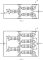
- Figure 2 illustrates a plan view of a die layout of a driver 126 configured in accordance with an embodiment of the present disclosure.
- An input of driver 126 may be operatively coupled with an output of upstream amplifier 124, in accordance with some embodiments.
- Another input of driver 126 may be operatively coupled with an output of an upstream source of a signal (Gate Control) external to architecture 100, in accordance with some embodiments.
- the Gate Control signal may control whether driver 126 is enabled or disabled, in accordance with some embodiments. In some instances, the Gate Control signal may be received from an EW system external to architecture 100.
- An output of driver 126 may be operatively coupled with a terminal J4, at which an output signal (e.g., a low-power output signal) of architecture 100 may be provided.
- Second sub-band channel chipset 101b includes a pre-driver 128, which may be of any suitable standard, custom, or proprietary electronic pre-driver configuration, as will be apparent in light of this disclosure.
- pre-driver 128 may be a single-stage pre-driver, whereas in other instances, it may be a multi-stage pre-driver (e.g., two-stage, three-stage, and so forth).
- pre-driver 128 and pre-driver 124 may be of the same configuration, whereas in other instances, they may be of different configurations.
- pre-driver 128 may be configured as any one, or combination, of the various pre-drivers described in U.S. Patent No.
- An input of pre-driver 128 may be operatively coupled with an output of upstream divider 122, in accordance with some embodiments.
- Another input of pre-driver 128 may be operatively coupled with an output of an upstream source of a signal (Gate Control) external to architecture 100, in accordance with some embodiments.
- the Gate Control signal may control whether pre-driver 128 is enabled or disabled, in accordance with some embodiments. In some instances, the Gate Control signal may be received from an EW system external to architecture 100.
- Second sub-band channel chipset 101b also includes a high-power amplifier (HPA) 130, which may be of any suitable standard, custom, or proprietary electronic amplifier configuration, as will be apparent in light of this disclosure.
- HPA 130 may be a single-stage HPA, whereas in other instances, it may be a multi-stage HPA (e.g., two-stage, three-stage, and so forth).
- HPA 130 may be configured as any one, or combination, of the various high-power amplifiers described in U.S. Patent No. 8,076,975, issued on December 13, 2011 , and titled "Broadband High Power Amplifier," which is incorporated by reference herein in its entirety.
- HPA 130 may be configured to amplify signals within the full K-band through K a -band instantaneous frequency range or any sub-range thereof.
- Figure 3 illustrates a plan view of a die layout of a HPA 130 configured in accordance with an embodiment of the present disclosure.
- An input of HPA 130 may be operatively coupled with an output of upstream pre-driver 128, in accordance with some embodiments.
- Another input of HPA 130 may be operatively coupled with an output of an upstream source of a signal (Gate Control) external to architecture 100, in accordance with some embodiments.
- the Gate Control signal may control whether HPA 130 is enabled or disabled, in accordance with some embodiments. In some instances, the Gate Control signal may be received from an EW system external to architecture 100.
- An output of HPA 130 may be operatively coupled with an output terminal J3, at which an output signal (e.g., a high-power output signal) of architecture 100 may be provided, in accordance with some embodiments.
- the output signal available at output terminal J3 may differ in power as compared to the signal available at terminal J4; for instance, the output signal at output terminal J3 may be greater in power level than the output signal at terminal J4, in accordance with some embodiments.
- the output signal at output terminal J3 may be of a different power level (e.g., a higher power level) than the output signal at output terminal J4.
- any (or all) of pre-driver 120, pre-driver 124, driver 126, pre-driver 128, and HPA 130 may be configured, for example, as a monolithic microwave integrated circuit (MMIC).
- MMIC monolithic microwave integrated circuit
- any (or all) of pre-driver 120, pre-driver 124, driver 126, pre-driver 128, and HPA 130 may include one or more gallium nitride (GaN)-based or other III-V semiconductor-based transistor devices.
- GaN gallium nitride
- transistor devices may be configured as gallium nitride-on-silicon carbide (GaN-on-SiC) devices, though the present disclosure is not intended to be so limited, as other suitable Group IV semiconductor substrates may be employed, in accordance with other embodiments.
- GaN-on-SiC gallium nitride-on-silicon carbide
- Other suitable configurations for the various components of architecture 100 will depend on a given application and will be apparent in light of this disclosure.
- the Gate Control signal(s) discussed above may be used in shutting off a given portion of either (or both) of channel chipsets 101a and 101b (e.g., any one or more of the various semiconductor dies of architecture 100). With such control over which of the individual semiconductor dies are in an on-state and which are in an off-state, tunable control over the gain and power levels of the output signal(s) of architecture 100 may be provided, in some cases realizing improvements in overall power and thermal management.
- any (or all) of pre-driver 120, pre-driver 124, driver 126, pre-driver 128, and HPA 130 may be physically and/or thermally coupled with a thermally conductive carrier 200.
- Carrier 200 generally may serve as a heat spreader for at least a portion of architecture 100.
- carrier 200 may be formed, in part or in whole, from any one, or combination, of thermally conductive materials that are coefficient of thermal expansion (CTE)-compatible with one or more of the various semiconductor dies of architecture 100.
- CTE coefficient of thermal expansion
- carrier 200 may include, in part or in whole, of a copper-molybdenum (Cu-Mo) alloy.
- the dimensions (e.g., z-thickness in the z-direction) of carrier 200 may be customized, as desired for a given target application or end-use.
- carrier 200 may have a z-thickness in the range of about 0.1-5 mm (e.g., about 0.1-2.5 mm, about 2.5-5 mm, or any other sub-range in the range of about 0.1-5 mm).
- carrier 200 may be a monolithic component.
- a monolithic carrier 200 may provide a continuous ground plane, which, at least in some cases, may help to realize a reduction in ground discontinuities between amplifier components which otherwise might cause gain dropouts.
- carrier 200 may be a plurality of elements that are affixed, adjoined, or otherwise disposed proximate one another, providing a multi-piece component.
- carrier 200 may include: (1) a first portion configured to host pre-driver 120; and (2) a second portion (e.g., a mezzanine portion) configured to host pre-driver 124, driver 126, pre-driver 128, and HPA 130.
- the second portion of such a carrier 200 may be considered, in a general sense, a super-carrier for semiconductor dies of architecture 100, configured, in accordance with some embodiments, to minimize (or otherwise reduce) ground plane discontinuities and associated gain reductions for operation at millimeter-wave frequencies.
- a super-carrier for semiconductor dies of architecture 100 configured, in accordance with some embodiments, to minimize (or otherwise reduce) ground plane discontinuities and associated gain reductions for operation at millimeter-wave frequencies.
- Other suitable materials, configurations, and dimensions for carrier 200 will depend on a given application and will be apparent in light of this disclosure.
- Physical and/or thermal coupling of the various semiconductor dies (e.g., pre-driver 120, pre-driver 124, driver 126, pre-driver 128, and HPA 130) of architecture 100 with carrier 200 may be provided via any of a wide range of suitable means.
- any of the various semiconductor dies of architecture 100 may be coupled with carrier 200 either directly or indirectly (e.g., with one or more intervening layers).
- a given semiconductor die of architecture 100 may be coupled with carrier 200 via a eutectic bonding process (e.g., eutectic soldering). More particularly, all (or some sub-set) of pre-driver 120, pre-driver 124, driver 126, pre-driver 128, and HPA 130 may be coupled with carrier 200 via eutectic bonding, in accordance with some embodiments.
- pre-driver 120 may be coupled with a first portion of carrier 200
- each of pre-driver 124, driver 126, pre-driver 128, and HPA 130 may be coupled with a second portion (e.g., a mezzanine portion) of carrier 200.
- pre-driver 124, driver 126, pre-driver 128, and HPA 130 may be so coupled with carrier 200 simultaneously (e.g., using a single eutectic bonding process to bond such semiconductor devices concurrently).
- carrier 200 e.g., using a single eutectic bonding process to bond such semiconductor devices concurrently.
- mechanical and/or thermal interface attachment of carrier 200 with, for instance, a housing e.g., such as housing 302, discussed below
- a housing e.g., such as housing 302, discussed below
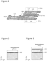
- Figure 5 illustrates a cross-sectional view of a semiconductor die coupled with carrier 200 via an intervening eutectic bonding layer 202, in accordance with an embodiment of the present disclosure.
- a eutectic bonding layer 202 may be disposed over a topography provided, in part or in whole, by carrier 200.
- Eutectic bonding layer 202 may include of one or more eutectic alloys, such as, for example, a gold-tin (Au-Sn) alloy.
- a Au-Sn alloy having a compositional ratio of 80 wt-% Au and 20 wt-% Sn may be utilized, providing for a eutectic temperature of about 280 °C ( ⁇ 5 °C).
- Eutectic bonding layer 202 may be disposed over a given underlying topography via any suitable standard, custom, or proprietary techniques, as will be apparent in light of this disclosure.
- eutectic bonding layer 202 may be formed via any one, or combination, of a solder pre-form process, a physical vapor deposition (PVD) process, such as sputtering or dual-source evaporation, or an electroplating process, among others.
- the dimensions (e.g., z-thickness in the z-direction) of a given eutectic bonding layer 202 may be customized, as desired for a given target application or end-use.
- a given eutectic bonding layer 202 may have a thickness in the range of about 0.01-0.05 mm (e.g., about 0.01-0.03 mm, about 0.03-0.05 mm, or any other sub-range in the range of about 0.01-0.05 mm).
- Other suitable materials, formation techniques, and dimensions for a given eutectic bonding layer 202 will depend on a given application and will be apparent in light of this disclosure.
- a given semiconductor die of architecture 100 may be disposed there over and coupled with carrier 200 via any suitable bonding process (e.g., heating, applying pressure, cooling, and so forth), in accordance with some embodiments.
- any suitable bonding process e.g., heating, applying pressure, cooling, and so forth
- eutectic bonding of a given semiconductor die with underlying carrier 200 may result, at least in some instances, in a mechanically compliant interface and electrical interconnection there between in a single process.
- one or more intervening layers optionally may be disposed between a given semiconductor die of architecture 100 and underlying carrier 200.
- FIG 6 illustrates a cross-sectional view of a semiconductor die disposed over carrier 200 and an intervening diamond layer 204, in accordance with an embodiment of the present disclosure.
- a diamond layer 204 may be coupled with carrier 200 via a eutectic bonding layer 202 (discussed above).
- a semiconductor die may be coupled with diamond layer 204 via another eutectic bonding layer 202.
- all (or some sub-set) of pre-driver 120, pre-driver 124, driver 126, pre-driver 128, and HPA 130 may have an intervening diamond layer 204 disposed between it and underlying carrier 200.
- HPA 130 alone may have an intervening diamond layer 204 disposed between it and underlying carrier 200.
- Diamond layer 204 may include a diamond material, which may be synthetic (e.g., formed via a chemical vapor deposition, or CVD, process) or naturally occurring (or both).
- diamond layer 204 may be configured as any one, or combination, of the various diamond layers described in U.S. Patent No. 8,669,812, issued on March 11, 2014 , and titled "High Power Amplifier," which is incorporated by reference herein in its entirety.
- one or more metallic coatings optionally may be disposed over a topography provided, in part or in whole, by diamond layer 204.
- diamond layer 204 may be customized, as desired for a given target application or end-use.
- diamond layer 204 may have a z-thickness in the range of about 0.1-0.5 mm (e.g., about 0.1-0.3 mm, about 0.3-0.5 mm, or any other sub-range in the range of about 0.1-0.5 mm).
- Other suitable materials, coupling techniques, and dimensions for optional diamond layer(s) 204 will depend on a given application and will be apparent in light of this disclosure.
- diamond layer 204 may be disposed there over and coupled with carrier 200 via any suitable bonding process (e.g., heating, applying pressure, cooling, and so forth), in accordance with some embodiments.
- a given semiconductor die of architecture 100 may be disposed there over and coupled with that diamond layer 204 via any suitable bonding process (e.g., heating, applying pressure, cooling, and so forth), in accordance with some embodiments.
- diamond material is a very good thermal conductor, and thus the presence of an optional diamond layer 204 between a given semiconductor die and underlying carrier 200 may facilitate conduction of heat generated by that die to carrier 200, in accordance with some embodiments.
- optional diamond layer 204 may be configured to serve, at least in part, as a heat spreader for a given semiconductor die coupled therewith.
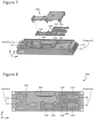
- Figures 7-8 illustrate exploded perspective and plan views, respectively, of a partially assembled amplifier module 300 configured in accordance with an embodiment of the present disclosure.
- Figures 9-10 illustrate front and rear perspective views, respectively, of an amplifier module 300 configured in accordance with an embodiment of the present disclosure.
- module 300 may include a housing 302.
- Housing 302 may include any one, or combination, of suitable construction material(s), such as aluminum (Al), titanium (Ti), a steel (e.g., carbon steel; stainless steel), or an alloy of any thereof, to name a few.
- suitable construction material(s) such as aluminum (Al), titanium (Ti), a steel (e.g., carbon steel; stainless steel), or an alloy of any thereof, to name a few.
- the dimensions (e.g., x-length in the x-direction; y-width in the y-direction; z-height in the z-direction) of housing 302 may be customized, as desired for a given target application or end-use.
- housing 302 may have an x-length in the range of about 3-5 inches (e.g., about 3-4 inches, about 4-5 inches, or any other sub-range in the range of about 3-5 inches). In an example case, housing 302 may have an x-length of about 4.4 inches ( ⁇ 0.5 inches). In another example case, housing 302 may have an x-length of about 3.54 inches ( ⁇ 0.5 inches).
- housing 302 may have a y-width in the range of about 0.5-3 inches (e.g., about 0.5-1.75 inches, about 1.75-3 inches, or any other sub-range in the range of about 0.5-3 inches). In an example case, housing 302 may have a y-width of about 2.2 inches ( ⁇ 0.5 inches). In another example case, housing 302 may have a y-width of about 1.00 inches ( ⁇ 0.5 inches).
- housing 302 may have a z-height in the range of about 0.2-2 inches (e.g., about 0.2-1.1 inches, about 1.1-2 inches, or any other sub-range in the range of about 0.2-2 inches). In an example case, housing 302 may have a z-height of about 0.40 inches ( ⁇ 0.2 inches).
- housing 302 may be configured to host carrier 200 and the one or more semiconductor dies of architecture 100 coupled therewith, in accordance with some embodiments.
- Carrier 200 optionally may be physically and/or thermally coupled with housing 302 via one or more intervening thermal interface layers, in accordance with some embodiments.
- a given thermal interface layer may be a layer of a thermally conductive epoxy or any other suitable standard, custom, or proprietary thermally conductive adhesive, as will be apparent in light of this disclosure.
- a given thermal interface layer may be a thermal pad including silicone or carbon graphite, among others.
- means for mechanical attachment such as fasteners and the like, may be employed additionally (or alternatively), and in some such instances may facilitate CTE-compliance.
- housing 302 may include one or more electrical connection ports 304 configured to be operative coupled with architecture 100 when installed within housing 302, in accordance with some embodiments.
- a given port 304 may be operatively coupled with either (or both) of amplifiers 108 and 114, for instance, to allow for V Out signal(s) to be output from architecture 100 to an EW system external to architecture 100.
- Module 300 further may include one or more cover portions 306 configured to be disposed over carrier 200 and its attendant semiconductor die(s), in accordance with some embodiments.
- a given cover portion 306 may be a monolithic component and configured to provide coverage for a similarly monolithic carrier 200, as discussed above.
- a given cover portion 306 may be a plurality of elements that are affixed, adjoined, or otherwise disposed proximate one another, providing a multi-piece component and configured to provide coverage for a similarly multi-piece carrier 200, as discussed above.
- a given cover portion 306 may be considered, in a general sense, a channelization cover for architecture 100.
- module 300 may include either (or both) a front housing cover 308 and a rear housing cover 310.
- a given housing cover 308 or 310 may be constructed with any of the example materials discussed above, for instance, with respect to housing 302, in accordance with some embodiments.
- architecture 100 optionally may be configured to be operatively coupled with one or more external circuits or devices.
- architecture 100 may be operatively coupled with DC power conditioning circuitry and/or DC routing circuitry, which may be configured as one or more topside and/or backside DC printed wire boards (PWBs).
- PWBs topside and/or backside DC printed wire boards
- the use of such PWB(s) may provide for routing DC bias signals and control signals through module 300 using minimal (or otherwise reduced) area.
- architecture 100 may be configured to be operatively coupled with one or more sensors (e.g., of an EW system).
- sensors e.g., of an EW system
- such additional circuits and devices may be housed, in part or in whole, by module 300, and housing 302 may be appropriately configured to that end, in accordance with some embodiments.
Landscapes
- Engineering & Computer Science (AREA)
- Power Engineering (AREA)
- Computer Networks & Wireless Communication (AREA)
- Signal Processing (AREA)
- Microelectronics & Electronic Packaging (AREA)
- Amplifiers (AREA)
- Chemical & Material Sciences (AREA)
- Materials Engineering (AREA)
Description
- The present disclosure relates to solid-state amplifiers and more particularly to high power radio frequency (RF) amplifiers.
- Electronic power amplifiers are typically designed to convert signals from a lower to a higher power level for output. Radio frequency (RF) power amplifiers are generally designed to operate on signals having frequencies in the range of 30 kHz to 100 GHz, which is commonly known as the RF band of the electromagnetic spectrum. Some RF power amplifiers are specifically designed to operate on signals in the frequency range of 1-30 GHz, which is known as the microwave sub-band of the RF band. Amplifiers designed to operate in the RF sub-band frequency range of 30-100 GHz are generally known as millimeter-wave amplifiers.
-
US2016049351A1 discloses a high power electronic device package constructed to include a high power electronic device having an epitaxial surface attached to a thermally conductive submount by a thermally conductive interface layer having a eutectic metal contact therein. Also disclosed is a gallium nitride high electron mobility transistor (GaN HEMT) having a transistor structure formed of a GaN thin film layer bonded to a thermally conductive host substrate via a thermally conductive interface layer disposed therebetween, and a method of forming the GaN HEMT. The GaN HEMTs can be used in such applications as, for example, power amplifiers with x-band radio frequency (RF) power outputs for micro-radar applications. -
US2013260703A1 discloses techniques and architecture for providing an ultra-wideband, multi-channel solid-state power amplifier architecture. In some embodiments, the architecture includes a power divider which splits an input signal and delivers that split signal to a plurality of downstream channel chipsets. Each channel chipset is configured to amplify a sub-band of the original full-band input signal and to provide the resultant amplified sub-band for downstream use, such as for transmission by an antenna operatively coupled with that channel. In the aggregate, the amplified sub-bands provide coverage of the same ultra-wideband frequency range of the original input signal, in some cases. In some embodiments, the architecture provides high radio frequency (RF) power with good amplifying efficiency and ultra-wide instantaneous frequency bandwidth performance in a small-form-factor package. In some instances, control circuitry is provided to control which chipset die(s) are enabled/disabled, thus providing control over gain and power levels of the output signal(s). - The invention is defined in the independent claim 1, defining a solid-state amplifier. Advantageous embodiments are set out in the dependent claims.
- The features and advantages described herein are not all-inclusive and, in particular, many additional features and advantages will be apparent to one of ordinary skill in the art in view of the drawings, specification, and claims. Moreover, it should be noted that the language used in the specification has been selected principally for readability and instructional purposes and not to limit the scope of the inventive subject matter. The scope of the invention is defined by the appended claims.
-
-
Figure 1 illustrates a block diagram of an amplifier circuit architecture configured in accordance with an embodiment of the present disclosure. -
Figure 2 illustrates a plan view of a die layout of a driver configured in accordance with an embodiment of the present disclosure. -
Figure 3 illustrates a plan view of a die layout of a high-power amplifier (HPA) configured in accordance with an embodiment of the present disclosure. -
Figure 4 illustrates a perspective view of several semiconductor dies disposed over a carrier configured in accordance with an embodiment of the present disclosure. -
Figure 5 illustrates a cross-sectional view of a semiconductor die coupled with a carrier via an intervening eutectic bonding layer, in accordance with an embodiment of the present disclosure. -
Figure 6 illustrates a cross-sectional view of a semiconductor die disposed over a carrier and an intervening diamond layer, in accordance with an embodiment of the present disclosure. -
Figures 7-8 illustrate exploded perspective and plan views, respectively, of a partially assembled amplifier module configured in accordance with an embodiment of the present disclosure. -
Figures 9-10 illustrate front and rear perspective views, respectively, of an amplifier module configured in accordance with an embodiment of the present disclosure. - These and other features of the present embodiments will be understood better by reading the following detailed description, taken together with the figures described herein. The accompanying drawings are not intended to be drawn to scale. In the drawings, each identical or nearly identical component that is illustrated in various figures may be represented by a like numeral. For purposes of clarity, not every component may be labeled in every drawing.
- A solid-state amplifier architecture is disclosed. An inventive embodiment of the solid-state amplifier is defined by independent claim 1. Not all embodiments introduced in the following detailed description fall under the scope of the invention. The scope of the invention is defined by the appended claims. In accordance with some embodiments, the disclosed architecture may include first and second channel chipsets configured to amplify either the entire instantaneous frequency band of a radio frequency (RF) input signal or, respectively, sub-bands thereof, which may be divided proportionally between the two chipsets. In some cases, the first and second chipsets may be configured to amplify frequencies in excess of the entire K-band and Ka-band frequencies simultaneously. To these ends, a given chipset may include one or more gallium nitride (GaN)-based monolithic microwave integrated circuit (MMIC) dies, in accordance with some embodiments. In some cases, the disclosed architecture may be configured to address a signal received, for instance, from an electronic warfare (EW) system to a log amplifier stage configured to output a signal to the EW system, in response to which the EW system may generate a RF signal for amplification by the architecture for transmission. To facilitate heat dissipation, the architecture may be coupled, in part or in whole, with a thermally conductive carrier, optionally with an intervening diamond heat spreader layer, in accordance with some embodiments. Numerous configurations and variations will be apparent in light of this disclosure.
- Of the various III-V semiconductor materials, gallium nitride (GaN) has particularly high power density characteristics that make it suitable for use, for example, in solid-state radio frequency (RF) power amplifiers that may be employed in transmitters utilized in advanced electronic warfare (EW) systems. However, such GaN-based devices generally have high power dissipation, and thermal management in the package design of these devices can be difficult. The continued demand for next-generation transmitters that provide sufficiently high levels of RF power over increasingly wider frequency bandwidths using architectures that exploit reduced size, weight, and power (SWaP), all within small form factor packages, will tend to exacerbate these non-trivial issues.
- Thus, and in accordance with some embodiments of the present disclosure, a solid-state amplifier architecture is disclosed. In accordance with some embodiments, the disclosed architecture may include first and second channel chipsets configured to amplify either the entire instantaneous frequency band of an RF input signal or, respectively, sub-bands thereof, which may be divided proportionally between the two chipsets. In some cases, the first and second chipsets may be configured to amplify frequencies in excess of the entire K-band to Ka-band instantaneous frequency bandwidth, or sub-bands of the entire instantaneous frequency bandwidth, proportionally divided among the chipsets. To these ends, a given chipset may include one or more gallium nitride (GaN)-based monolithic microwave integrated circuit (MMIC) dies, in accordance with some embodiments. In some cases, the disclosed architecture may be configured to address a signal received, for instance, from an electronic warfare (EW) system to a log amplifier stage configured to output a signal to the EW system, in response to which the EW system may generate a RF signal for amplification by the architecture for transmission. To facilitate heat dissipation, the architecture may be coupled, in part or in whole, with a thermally conductive carrier, optionally with an intervening diamond heat spreader layer, in accordance with some embodiments.
- In accordance with some embodiments, the disclosed amplifier architecture may be configured for use in providing a solid-state power amplifier device configured to operate at millimeter-wave frequencies in a manner which provides high power density amplification over several full bands (e.g., K-band and Ka-band) of instantaneous frequency. In accordance with some embodiments, such an amplifier device may be configured to deliver in the range of about 5-30 W (or greater) of RF power over the entire instantaneous frequency bandwidth encompassing in excess of K-band through Ka-band frequency ranges, in some instances with continuous wave (CW) performance. In accordance with some embodiments, the disclosed architecture may include a detector log amplifier configured to provide a receive-input capability by which a signal indicative of a detected threat or other stimulus of interest may be provided for rapid processing, and in response to which an associated transmit signal can be initiated via the transmit input of the architecture.
- As discussed herein, power consumption and thermal management within the context of the disclosed architecture may be provided in any of a wide variety of ways. For example, in some embodiments, the disclosed architecture may include MMIC dies that are spatially distributed in a manner that spreads out the heat generated by the individual transistor devices. In some embodiments, the disclosed architecture may be coupled, in part or in whole, with a thermally conductive carrier configured to distribute heat generated by the devices coupled thereto. In some embodiments, a diamond heat spreader optionally may be disposed under a given MMIC die, providing heat extraction and contributing to spreading of the thermal load. In some embodiments, the disclosed architecture may be configured to allow for direct control over which constituent semiconductor die(s) of a given channel chipset are enabled/disabled at a given time. Such individualized on/off control of all (or some sub-set) of the constituent MMIC dies may provide for fine control over the gain and power levels of the output signal(s), in accordance with some embodiments. As will be appreciated in light of this disclosure, the ability to quickly and efficiently toggle operation of the solid-state architecture via one or more gate control signals, for instance, may reduce the amount of excess on-time of all (or some sub-set) of the constituent MMIC dies and thus may realize reductions in DC power consumption and, consequently, the amount of heat generated by the architecture. In accordance with some embodiments, the improved heat extraction performance and management of the total thermal load may serve to minimize (or otherwise reduce) the thermal rise at the junctions of the GaN-based transistor devices, and thus may realize improvements in device performance (e.g., more efficient generation of high-power RF signals) and reliability, at least in some instances.
- In accordance with some embodiments, the disclosed architecture may include MMIC dies coupled to a thermally conductive carrier which have undergone one or more coefficient of thermal expansion (CTE)-compliant die attachment processes and thus can withstand temperature cycling stresses without delamination. Thus, at least in some instances, the MMIC dies of the disclosed architecture need not be physically fastened to their host carrier or host module via screws or the like, though such fasteners optionally may be employed, if desired. In accordance with some embodiments, a reduction in the quantity (or outright omission) of such fasteners may realize a reduction in the areal footprint of the carrier, thereby contributing to a reduction in overall package size while still accommodating the thermal management needs of the semiconductor dies coupled therewith.
- In accordance with some embodiments, the disclosed architecture may be utilized in providing a power amplifier which exhibits both high RF power and wide instantaneous frequency bandwidth performance in a compact, small form factor transmitter package that does not require extensive tuning or a high degree of touch labor during module assembly. In some instances, the resultant reduced-SWaP transmitter may be suitable for application, for example, in an electronic warfare (EW) system. It should be noted, however, that an amplifier device configured as variously described herein need not be limited only to transmission capabilities, as in accordance with some embodiments, both transmit and receive (e.g., transceiver) capabilities may be provisioned.
-
Figure 1 illustrates a block diagram of anamplifier circuit architecture 100 configured in accordance with an embodiment of the present disclosure. As can be seen,architecture 100 includes two input terminals (J1 and J2) and two output terminals (J3 and J4). In accordance with some embodiments, input terminal J2 may be configured to receive a first signal, for example, from an electronic warfare (EW) system external toarchitecture 100. In some cases, the first signal received at input terminal J2 may be one which was output by the EW system, for instance, in response to a detected threat (e.g., as sensed by a sensor of the EW system). In turn, either or both ofamplifiers 108 and 114 (discussed below) may output to the EW system a signal (VOut), for instance, indicative of the amplitude level of the first signal received at input terminal J2. In response, the EW system may output a second signal that may be received at input terminal J1 ofarchitecture 100 for amplification thereby. Output terminals J3 and J4 ofarchitecture 100 each may be configured to output one of two output RF power levels, in accordance with some embodiments. As further discussed herein,architecture 100 may be configured to provide gain for a signal propagating from input terminal J1 to output terminal J3, in accordance with some embodiments. In accordance with some embodiments,architecture 100 may be configured for operation in excess of K-band through Ka-band instantaneous frequency bandwidth. - As can be seen,
architecture 100 includes aswitch 102, which may be a single-pole, double-throw (SPDT) switch or any other suitable switch, as will be apparent in light of this disclosure. An input ofswitch 102 may be operatively coupled with an upstream input terminal J1, in accordance with some embodiments. As previously noted, a signal output by an EW system external toarchitecture 100 may be received at input terminal J1 for amplification and transmission, in accordance with some embodiments. Another input ofswitch 102 may be operatively coupled with the output of an upstream source of a signal (Input Enable) external toarchitecture 100, in accordance with some embodiments. The Input Enable signal may control whether a signal received at input terminal J1 from an external EW system is: (1) delivered to ground through a resistor 104, the particular type and electrical resistance value of which may be customized, as desired for a given target application or end-use; or (2) propagated througharchitecture 100, in accordance with some embodiments. -
Architecture 100 further includes aswitch 106, which may be a SPDT switch or any other suitable switch, as will be apparent in light of this disclosure. In some instances,switch 106 and switch 102 may be of the same configuration, whereas in other instances, they may be of different configurations. An input ofswitch 106 may be operatively coupled with an upstream input terminal J2, in accordance with some embodiments. As previously noted, a signal output by an EW system external toarchitecture 100 may be received at input terminal J2. In some cases, such a signal may be output by the EW system, for instance, in response to a detected threat (e.g., as sensed by a sensor of the EW system). Another input ofswitch 106 may be operatively coupled with an output ofupstream switch 102, in accordance with some embodiments. Another input ofswitch 106 may be operatively coupled with an upstream source of a signal (Path Select) external toarchitecture 100, in accordance with some embodiments. The Path Select signal may control whether a signal received at input terminal J1 and passed throughswitch 102 is propagated througharchitecture 100, in accordance with some embodiments. -
Architecture 100 also includes anamplifier 108, which may be configured as a successive detection logarithmic video amplifier (SDLVA) or any other suitable standard, custom, or proprietary amplifier, as will be apparent in light of this disclosure. An input ofamplifier 108 may be operatively coupled with a coupler 110 (discussed below), in accordance with some embodiments. As previously noted,amplifier 108 may be configured to output a signal (VOut), for instance, to an EW system external toarchitecture 100. The VOut signal ofamplifier 108 may be indicative of the amplitude level of the signal received at input terminal J2, in accordance with some embodiments. -
Architecture 100 further includes acoupler 110, which may be configured as any suitable standard, custom, or proprietary coupler, as will be apparent in light of this disclosure. An input ofcoupler 110 may be operatively coupled with an output ofupstream switch 106, in accordance with some embodiments. An output ofcoupler 110 may be operatively coupled with an input ofdownstream amplifier 108, in accordance with some embodiments. -
Architecture 100 further includes anamplifier 112, which may be configured as a low-noise amplifier (LNA) or any other suitable standard, custom, or proprietary amplifier, as will be apparent in light of this disclosure.Amplifier 112 may include, in part or in whole, a gallium nitride (GaN), gallium arsenide (GaAs), or other III-V semiconductor-based transistor device, in accordance with some embodiments. An input ofamplifier 112 may be operatively coupled with an output ofupstream coupler 110, in accordance with some embodiments. -
Architecture 100 also includes anamplifier 114, which may be configured as a SDLVA or any other suitable standard, custom, or proprietary amplifier, as will be apparent in light of this disclosure. In some instances,amplifier 114 andamplifier 108 may be of the same configuration, whereas in other instances, they may be of different configurations. An input ofamplifier 114 may be operatively coupled with a coupler 116 (discussed below), In accordance with some embodiments. As previously noted,amplifier 114 may be configured to output a signal (VOut), for instance, to an EW system external toarchitecture 100. The VOut signal ofamplifier 114 may be indicative of the amplitude level of the signal received at input terminal J2, in accordance with some embodiments. -
Architecture 100 further includes acoupler 116, which may be configured as any suitable standard, custom, or proprietary coupler, as will be apparent in light of this disclosure. In some instances,coupler 116 andcoupler 110 may be of the same configuration, whereas in other instances, they may be of different configurations. An input ofcoupler 116 may be operatively coupled with an output ofupstream amplifier 112, in accordance with some embodiments. An output ofcoupler 116 may be operatively coupled with an input ofdownstream amplifier 114, in accordance with some embodiments. -
Architecture 100 also includes anattenuator 118, which may be configured as a variable voltage attenuator (VVA) or any other suitable standard, custom, or proprietary attenuator, as will be apparent in light of this disclosure. An input ofattenuator 118 may be operatively coupled with an output ofupstream coupler 116, in accordance with some embodiments. -
Architecture 100 further includes a pre-driver 120, which may be of any suitable standard, custom, or proprietary pre-driver configuration, as will be apparent in light of this disclosure. In some instances,pre-driver 120 may be a single-stage pre-driver, whereas in other instances, it may be a multi-stage pre-driver (e.g., two-stage, three-stage, and so forth). An input ofpre-driver 120 may be operatively coupled with an output ofupstream attenuator 118, in accordance with some embodiments. Another input ofpre-driver 120 may be operatively coupled with an upstream source of a signal (Gate Control) external toarchitecture 100, in accordance with some embodiments. The Gate Control signal may control whetherpre-driver 120 is enabled or disabled, in accordance with some embodiments. In some instances, the Gate Control signal may be received from an EW system external toarchitecture 100. -
Architecture 100 also includes adivider 122, which may be of any suitable standard, custom, or proprietary signal splitter configuration, as will be apparent in light of this disclosure. In some embodiments,divider 122 may be a passive power divider, such as, for example, an in-phase Wilkinson power divider, including one or more resistors. In some other embodiments,divider 122 may be an active power divider configured to provide gain in addition to power division of a signal. In some instances,divider 122 may be configured to provide an approximately 50%/50% power split of the signal input thereto, though even power splitting is not necessary to operation ofarchitecture 100. In accordance with some embodiments,divider 122 may be configured as any one, or combination, of the various dividers described inU.S. Patent No. 8,989,683, issued on March 24, 2015 , and titled "Ultra-Wideband High Power Amplifier Architecture," which is incorporated by reference herein in its entirety. An input ofdivider 122 may be operatively coupled with an output ofupstream pre-driver 120, in accordance with some embodiments. In some embodiments,divider 122 may be a two-channel (2:1) splitter configured to split the signal received fromupstream amplifier 120 into two signals, one of which is provided to a downstream sub-band channel chipset 101a (discussed below) and the other of which is provided to a downstream sub-band channel chipset 101a (discussed below). - As can be seen further from
Figure 1 ,architecture 100 also includes: (1) a first sub-band channel chipset 101a; and (2) a secondsub-band channel chipset 101b. As explained above,divider 122 may split a received input signal and deliver that split signal todownstream channel chipsets 101a and 101b, in accordance with some embodiments. Eachsuch channel chipset 101a and 101b may be configured to amplify either the full instantaneous frequency band or a narrower frequency sub-band (channel) of the input signal which it receives. For instance, first sub-band channel chipset 101a may be configured, in accordance with some embodiments, to amplify frequencies of the input signal (received from divider 122) in at least a portion of the full instantaneous K-band through Ka-band range and output the resultant signal at output terminal J4. Secondsub-band channel chipset 101b may be configured, in accordance with some embodiments, to amplify frequencies of the input signal (received from divider 122) in the full instantaneous K-band through Ka-band range or a sub-set of the full range and output the resultant signal at output terminal J3. Thus, in a more general sense,channel chipsets 101a and 101b may be configured to partition and amplify the full, instantaneous operating bandwidth of the original input signal (received from divider 122), in accordance with some embodiments. In some cases, the resultant amplified sub-bands may be delivered to downstream output terminals J3 and J4, for example, for transmission by antennas associated with thechannel chipsets 101a and 101b. - First sub-band channel chipset 101a includes a pre-driver 124, which may be of any suitable standard, custom, or proprietary electronic pre-driver configuration, as will be apparent in light of this disclosure. In some instances,
pre-driver 124 may be a single-stage pre-driver, whereas in other instances, it may be a multi-stage pre-driver (e.g., two-stage, three-stage, and so forth). In accordance with some embodiments,pre-driver 124 may be configured as any one, or combination, of the various pre-drivers described inU.S. Patent No. 7,924,097, issued on April 12, 2011 , and titled "Solid-State Ultra-Wideband Microwave Power Amplifier Employing Modular Non-Uniform Distributed Amplifier Elements," which is incorporated by reference herein in its entirety. An input ofpre-driver 124 may be operatively coupled with an output ofupstream divider 122, in accordance with some embodiments. Another input ofpre-driver 124 may be operatively coupled with an output of an upstream source of a signal (Gate Control) external toarchitecture 100, in accordance with some embodiments. The Gate Control signal may control whetherpre-driver 124 is enabled or disabled, in accordance with some embodiments. In some instances, the Gate Control signal may be received from an EW system external toarchitecture 100. - First sub-band channel chipset 101a also includes a
driver 126, which may be of any suitable standard, custom, or proprietary electronic driver configuration, as will be apparent in light of this disclosure. In some instances,driver 126 may be a single-stage driver, whereas in other instances, it may be a multi-stage driver (e.g., two-stage, three-stage, and so forth). In accordance with some embodiments,driver 126 may be configured as any one, or combination, of the various drivers described inU.S. Patent No. 8,989,683 , which is incorporated by reference above. In some cases,driver 126 may be configured to amplify signals within the full K-band through Ka-band instantaneous frequency range or any sub-range thereof.Figure 2 illustrates a plan view of a die layout of adriver 126 configured in accordance with an embodiment of the present disclosure. An input ofdriver 126 may be operatively coupled with an output ofupstream amplifier 124, in accordance with some embodiments. Another input ofdriver 126 may be operatively coupled with an output of an upstream source of a signal (Gate Control) external toarchitecture 100, in accordance with some embodiments. The Gate Control signal may control whetherdriver 126 is enabled or disabled, in accordance with some embodiments. In some instances, the Gate Control signal may be received from an EW system external toarchitecture 100. An output ofdriver 126 may be operatively coupled with a terminal J4, at which an output signal (e.g., a low-power output signal) ofarchitecture 100 may be provided. - Second
sub-band channel chipset 101b includes a pre-driver 128, which may be of any suitable standard, custom, or proprietary electronic pre-driver configuration, as will be apparent in light of this disclosure. In some instances,pre-driver 128 may be a single-stage pre-driver, whereas in other instances, it may be a multi-stage pre-driver (e.g., two-stage, three-stage, and so forth). In some instances,pre-driver 128 and pre-driver 124 may be of the same configuration, whereas in other instances, they may be of different configurations. In accordance with some embodiments,pre-driver 128 may be configured as any one, or combination, of the various pre-drivers described inU.S. Patent No. 7,924,097 , which is incorporated by reference above. An input ofpre-driver 128 may be operatively coupled with an output ofupstream divider 122, in accordance with some embodiments. Another input ofpre-driver 128 may be operatively coupled with an output of an upstream source of a signal (Gate Control) external toarchitecture 100, in accordance with some embodiments. The Gate Control signal may control whetherpre-driver 128 is enabled or disabled, in accordance with some embodiments. In some instances, the Gate Control signal may be received from an EW system external toarchitecture 100. - Second
sub-band channel chipset 101b also includes a high-power amplifier (HPA) 130, which may be of any suitable standard, custom, or proprietary electronic amplifier configuration, as will be apparent in light of this disclosure. In some instances,HPA 130 may be a single-stage HPA, whereas in other instances, it may be a multi-stage HPA (e.g., two-stage, three-stage, and so forth). In accordance with some embodiments,HPA 130 may be configured as any one, or combination, of the various high-power amplifiers described inU.S. Patent No. 8,076,975, issued on December 13, 2011 , and titled "Broadband High Power Amplifier," which is incorporated by reference herein in its entirety. In some cases,HPA 130 may be configured to amplify signals within the full K-band through Ka-band instantaneous frequency range or any sub-range thereof.Figure 3 illustrates a plan view of a die layout of aHPA 130 configured in accordance with an embodiment of the present disclosure. An input ofHPA 130 may be operatively coupled with an output ofupstream pre-driver 128, in accordance with some embodiments. Another input ofHPA 130 may be operatively coupled with an output of an upstream source of a signal (Gate Control) external toarchitecture 100, in accordance with some embodiments. The Gate Control signal may control whetherHPA 130 is enabled or disabled, in accordance with some embodiments. In some instances, the Gate Control signal may be received from an EW system external toarchitecture 100. An output ofHPA 130 may be operatively coupled with an output terminal J3, at which an output signal (e.g., a high-power output signal) ofarchitecture 100 may be provided, in accordance with some embodiments. The output signal available at output terminal J3 may differ in power as compared to the signal available at terminal J4; for instance, the output signal at output terminal J3 may be greater in power level than the output signal at terminal J4, in accordance with some embodiments. In accordance with some embodiments, the output signal at output terminal J3 may be of a different power level (e.g., a higher power level) than the output signal at output terminal J4. - In accordance with some embodiments, any (or all) of
pre-driver 120,pre-driver 124,driver 126,pre-driver 128, andHPA 130 may be configured, for example, as a monolithic microwave integrated circuit (MMIC). In accordance with some embodiments, any (or all) ofpre-driver 120,pre-driver 124,driver 126,pre-driver 128, andHPA 130 may include one or more gallium nitride (GaN)-based or other III-V semiconductor-based transistor devices. In some cases, such transistor devices may be configured as gallium nitride-on-silicon carbide (GaN-on-SiC) devices, though the present disclosure is not intended to be so limited, as other suitable Group IV semiconductor substrates may be employed, in accordance with other embodiments. Other suitable configurations for the various components ofarchitecture 100 will depend on a given application and will be apparent in light of this disclosure. - As will be appreciated in light of this disclosure, the Gate Control signal(s) discussed above may be used in shutting off a given portion of either (or both) of
channel chipsets 101a and 101b (e.g., any one or more of the various semiconductor dies of architecture 100). With such control over which of the individual semiconductor dies are in an on-state and which are in an off-state, tunable control over the gain and power levels of the output signal(s) ofarchitecture 100 may be provided, in some cases realizing improvements in overall power and thermal management. - In order to provide thermal management for
architecture 100, in part or in whole, any (or all) ofpre-driver 120,pre-driver 124,driver 126,pre-driver 128, andHPA 130 may be physically and/or thermally coupled with a thermallyconductive carrier 200. For instance, considerFigure 4 , which illustrates a perspective view of several semiconductor dies disposed over acarrier 200 configured in accordance with an embodiment of the present disclosure.Carrier 200 generally may serve as a heat spreader for at least a portion ofarchitecture 100. To that end,carrier 200 may be formed, in part or in whole, from any one, or combination, of thermally conductive materials that are coefficient of thermal expansion (CTE)-compatible with one or more of the various semiconductor dies ofarchitecture 100. In an example embodiment,carrier 200 may include, in part or in whole, of a copper-molybdenum (Cu-Mo) alloy. The dimensions (e.g., z-thickness in the z-direction) ofcarrier 200 may be customized, as desired for a given target application or end-use. In some cases,carrier 200 may have a z-thickness in the range of about 0.1-5 mm (e.g., about 0.1-2.5 mm, about 2.5-5 mm, or any other sub-range in the range of about 0.1-5 mm). - In some embodiments,
carrier 200 may be a monolithic component. As will be appreciated in light of this disclosure, amonolithic carrier 200 may provide a continuous ground plane, which, at least in some cases, may help to realize a reduction in ground discontinuities between amplifier components which otherwise might cause gain dropouts. In other embodiments, however,carrier 200 may be a plurality of elements that are affixed, adjoined, or otherwise disposed proximate one another, providing a multi-piece component. For instance, in an example case,carrier 200 may include: (1) a first portion configured to host pre-driver 120; and (2) a second portion (e.g., a mezzanine portion) configured to host pre-driver 124,driver 126,pre-driver 128, andHPA 130. Thus, the second portion of such acarrier 200 may be considered, in a general sense, a super-carrier for semiconductor dies ofarchitecture 100, configured, in accordance with some embodiments, to minimize (or otherwise reduce) ground plane discontinuities and associated gain reductions for operation at millimeter-wave frequencies. Other suitable materials, configurations, and dimensions forcarrier 200 will depend on a given application and will be apparent in light of this disclosure. - Physical and/or thermal coupling of the various semiconductor dies (e.g.,
pre-driver 120,pre-driver 124,driver 126,pre-driver 128, and HPA 130) ofarchitecture 100 withcarrier 200 may be provided via any of a wide range of suitable means. Moreover, any of the various semiconductor dies ofarchitecture 100 may be coupled withcarrier 200 either directly or indirectly (e.g., with one or more intervening layers). - In accordance with some embodiments, a given semiconductor die of
architecture 100 may be coupled withcarrier 200 via a eutectic bonding process (e.g., eutectic soldering). More particularly, all (or some sub-set) ofpre-driver 120,pre-driver 124,driver 126,pre-driver 128, andHPA 130 may be coupled withcarrier 200 via eutectic bonding, in accordance with some embodiments. In a specific example case,pre-driver 120 may be coupled with a first portion ofcarrier 200, whereas each ofpre-driver 124,driver 126,pre-driver 128, andHPA 130 may be coupled with a second portion (e.g., a mezzanine portion) ofcarrier 200. In some instances,pre-driver 124,driver 126,pre-driver 128, andHPA 130 may be so coupled withcarrier 200 simultaneously (e.g., using a single eutectic bonding process to bond such semiconductor devices concurrently). In providing simultaneous attachment of such dies tocarrier 200, mechanical and/or thermal interface attachment ofcarrier 200 with, for instance, a housing (e.g., such ashousing 302, discussed below) may be provided in a CTE-compliant manner, in accordance with some embodiments. -
Figure 5 illustrates a cross-sectional view of a semiconductor die coupled withcarrier 200 via an interveningeutectic bonding layer 202, in accordance with an embodiment of the present disclosure. As can be seen here, aeutectic bonding layer 202 may be disposed over a topography provided, in part or in whole, bycarrier 200.Eutectic bonding layer 202 may include of one or more eutectic alloys, such as, for example, a gold-tin (Au-Sn) alloy. In a specific example case, a Au-Sn alloy having a compositional ratio of 80 wt-% Au and 20 wt-% Sn may be utilized, providing for a eutectic temperature of about 280 °C (± 5 °C). -
Eutectic bonding layer 202 may be disposed over a given underlying topography via any suitable standard, custom, or proprietary techniques, as will be apparent in light of this disclosure. In accordance with some embodiments,eutectic bonding layer 202 may be formed via any one, or combination, of a solder pre-form process, a physical vapor deposition (PVD) process, such as sputtering or dual-source evaporation, or an electroplating process, among others. Moreover, the dimensions (e.g., z-thickness in the z-direction) of a giveneutectic bonding layer 202 may be customized, as desired for a given target application or end-use. In some cases, a giveneutectic bonding layer 202 may have a thickness in the range of about 0.01-0.05 mm (e.g., about 0.01-0.03 mm, about 0.03-0.05 mm, or any other sub-range in the range of about 0.01-0.05 mm). Other suitable materials, formation techniques, and dimensions for a giveneutectic bonding layer 202 will depend on a given application and will be apparent in light of this disclosure. - With a given
eutectic bonding layer 202 in place, a given semiconductor die ofarchitecture 100 may be disposed there over and coupled withcarrier 200 via any suitable bonding process (e.g., heating, applying pressure, cooling, and so forth), in accordance with some embodiments. As will be appreciated in light of this disclosure, eutectic bonding of a given semiconductor die withunderlying carrier 200 may result, at least in some instances, in a mechanically compliant interface and electrical interconnection there between in a single process. - As noted above, one or more intervening layers optionally may be disposed between a given semiconductor die of
architecture 100 andunderlying carrier 200. For instance, considerFigure 6 , which illustrates a cross-sectional view of a semiconductor die disposed overcarrier 200 and an interveningdiamond layer 204, in accordance with an embodiment of the present disclosure. As can be seen here, adiamond layer 204 may be coupled withcarrier 200 via a eutectic bonding layer 202 (discussed above). In turn, a semiconductor die may be coupled withdiamond layer 204 via anothereutectic bonding layer 202. In accordance with some embodiments, all (or some sub-set) ofpre-driver 120,pre-driver 124,driver 126,pre-driver 128, andHPA 130 may have an interveningdiamond layer 204 disposed between it andunderlying carrier 200. In a specific example embodiment,HPA 130 alone may have an interveningdiamond layer 204 disposed between it andunderlying carrier 200. -
Diamond layer 204 may include a diamond material, which may be synthetic (e.g., formed via a chemical vapor deposition, or CVD, process) or naturally occurring (or both). In accordance with some embodiments,diamond layer 204 may be configured as any one, or combination, of the various diamond layers described inU.S. Patent No. 8,669,812, issued on March 11, 2014 , and titled "High Power Amplifier," which is incorporated by reference herein in its entirety. In some cases, one or more metallic coatings optionally may be disposed over a topography provided, in part or in whole, bydiamond layer 204. The dimensions (e.g., z-thickness in the z-direction) ofdiamond layer 204 may be customized, as desired for a given target application or end-use. In some cases,diamond layer 204 may have a z-thickness in the range of about 0.1-0.5 mm (e.g., about 0.1-0.3 mm, about 0.3-0.5 mm, or any other sub-range in the range of about 0.1-0.5 mm). Other suitable materials, coupling techniques, and dimensions for optional diamond layer(s) 204 will depend on a given application and will be apparent in light of this disclosure. - With a first
eutectic bonding layer 202 in place,diamond layer 204 may be disposed there over and coupled withcarrier 200 via any suitable bonding process (e.g., heating, applying pressure, cooling, and so forth), in accordance with some embodiments. Withdiamond layer 204 in place, a given semiconductor die ofarchitecture 100 may be disposed there over and coupled with thatdiamond layer 204 via any suitable bonding process (e.g., heating, applying pressure, cooling, and so forth), in accordance with some embodiments. As will be appreciated in light of this disclosure, diamond material is a very good thermal conductor, and thus the presence of anoptional diamond layer 204 between a given semiconductor die andunderlying carrier 200 may facilitate conduction of heat generated by that die tocarrier 200, in accordance with some embodiments. In a general sense,optional diamond layer 204 may be configured to serve, at least in part, as a heat spreader for a given semiconductor die coupled therewith. -
Figures 7-8 illustrate exploded perspective and plan views, respectively, of a partially assembledamplifier module 300 configured in accordance with an embodiment of the present disclosure.Figures 9-10 illustrate front and rear perspective views, respectively, of anamplifier module 300 configured in accordance with an embodiment of the present disclosure. - As can be seen from these figures,
module 300 may include ahousing 302.Housing 302 may include any one, or combination, of suitable construction material(s), such as aluminum (Al), titanium (Ti), a steel (e.g., carbon steel; stainless steel), or an alloy of any thereof, to name a few. Moreover, the dimensions (e.g., x-length in the x-direction; y-width in the y-direction; z-height in the z-direction) ofhousing 302 may be customized, as desired for a given target application or end-use. - In some cases,
housing 302 may have an x-length in the range of about 3-5 inches (e.g., about 3-4 inches, about 4-5 inches, or any other sub-range in the range of about 3-5 inches). In an example case,housing 302 may have an x-length of about 4.4 inches (± 0.5 inches). In another example case,housing 302 may have an x-length of about 3.54 inches (± 0.5 inches). - In some cases,
housing 302 may have a y-width in the range of about 0.5-3 inches (e.g., about 0.5-1.75 inches, about 1.75-3 inches, or any other sub-range in the range of about 0.5-3 inches). In an example case,housing 302 may have a y-width of about 2.2 inches (± 0.5 inches). In another example case,housing 302 may have a y-width of about 1.00 inches (± 0.5 inches). - In some cases,
housing 302 may have a z-height in the range of about 0.2-2 inches (e.g., about 0.2-1.1 inches, about 1.1-2 inches, or any other sub-range in the range of about 0.2-2 inches). In an example case,housing 302 may have a z-height of about 0.40 inches (± 0.2 inches). - As can be seen,
housing 302 may be configured to hostcarrier 200 and the one or more semiconductor dies ofarchitecture 100 coupled therewith, in accordance with some embodiments.Carrier 200 optionally may be physically and/or thermally coupled withhousing 302 via one or more intervening thermal interface layers, in accordance with some embodiments. In some cases, a given thermal interface layer may be a layer of a thermally conductive epoxy or any other suitable standard, custom, or proprietary thermally conductive adhesive, as will be apparent in light of this disclosure. In some cases, a given thermal interface layer may be a thermal pad including silicone or carbon graphite, among others. In accordance with some embodiments, means for mechanical attachment, such as fasteners and the like, may be employed additionally (or alternatively), and in some such instances may facilitate CTE-compliance. - As can be seen further,
housing 302 may include one or moreelectrical connection ports 304 configured to be operative coupled witharchitecture 100 when installed withinhousing 302, in accordance with some embodiments. In some cases, a givenport 304 may be operatively coupled with either (or both) ofamplifiers architecture 100 to an EW system external toarchitecture 100. -
Module 300 further may include one ormore cover portions 306 configured to be disposed overcarrier 200 and its attendant semiconductor die(s), in accordance with some embodiments. In some embodiments, a givencover portion 306 may be a monolithic component and configured to provide coverage for a similarlymonolithic carrier 200, as discussed above. In other embodiments, a givencover portion 306 may be a plurality of elements that are affixed, adjoined, or otherwise disposed proximate one another, providing a multi-piece component and configured to provide coverage for a similarlymulti-piece carrier 200, as discussed above. In accordance with some embodiments, a givencover portion 306 may be considered, in a general sense, a channelization cover forarchitecture 100. - As can be seen further from these figures,
module 300 may include either (or both) afront housing cover 308 and arear housing cover 310. A givenhousing cover housing 302, in accordance with some embodiments. - In accordance with some embodiments,
architecture 100 optionally may be configured to be operatively coupled with one or more external circuits or devices. For instance, in some embodiments,architecture 100 may be operatively coupled with DC power conditioning circuitry and/or DC routing circuitry, which may be configured as one or more topside and/or backside DC printed wire boards (PWBs). In some cases, the use of such PWB(s) may provide for routing DC bias signals and control signals throughmodule 300 using minimal (or otherwise reduced) area. In some embodiments,architecture 100 may be configured to be operatively coupled with one or more sensors (e.g., of an EW system). In some cases when optionally included, such additional circuits and devices may be housed, in part or in whole, bymodule 300, andhousing 302 may be appropriately configured to that end, in accordance with some embodiments. - The foregoing description of example embodiments has been presented for the purposes of illustration and description. It is not intended to be exhaustive or to limit the present disclosure to the precise forms disclosed. Many modifications and variations are possible in light of this disclosure. It is intended that the scope of the present disclosure be limited not by this detailed description, but rather by the claims appended hereto.
Claims (10)
- A solid-state amplifier (100) comprising:a first input (J2) configured to receive a first radio frequency (RF) signal from a first source external to the amplifier;a second input (J1) configured to receive a second RF signal from a second source external to the amplifier;a first chipset (101a) configured to amplify a first sub-band of the second RF signal, the first chipset comprising a pre-driver (124) and a driver (126) operatively coupled with an output of the pre-driver, wherein at least one of the pre-driver and the driver is configured as a gallium nitride (GaN)-based monolithic microwave integrated circuit (MMIC);a second chipset configured to amplify a second sub-band of the second RF signal, the second chipset comprising a pre-driver (128) and a high power amplifier (130) operatively coupled with an output of the pre-driver, wherein at least one of the pre-driver and the high power amplifier is configured as a gallium nitride (GaN)-based monolithic microwave integrated circuit (MMIC);a carrier (200) coupled with at least one of the first chipset and the second chipset, wherein the carrier comprises a thermally conductive material; anda diamond layer (204) disposed between the carrier and at least one semiconductor die of at least one of the first chipset and the second chipset, wherein:the carrier is coupled with the diamond layer via a first eutectic bonding layer (202); andthe at least one semiconductor die is coupled with the diamond layer via a second eutectic bonding layer (202).
- The solid-state amplifier of claim 1 further comprising at least one successive detection logarithmic video amplifier (SDLVA) (108) configured to receive the first RF signal and output a signal indicative of an amplitude level of the first RF signal received by the first input (J2).
- The solid-state amplifier of claim 2, wherein the second input (J1) is configured to receive the second RF signal in response to receipt of the signal indicative of the amplitude level by the second source external to the amplifier.
- The solid-state amplifier of claim 1, wherein the carrier (200) constitutes a monolithic component.
- The solid-state amplifier of claim 1, wherein the carrier (200) constitutes a multi-piece component comprising at least:a first portion; anda second portion to which both the first chipset and the second chipset are coupled.
- The solid-state amplifier of claim 1, wherein the carrier (200) comprises a copper-molybdenum (Cu-Mo) alloy.
- The solid-state amplifier of claim 1 further comprising a divider (122) configured to split the second RF signal for delivery to the first chipset and the second chipset.
- The solid-state amplifier of claim 7 further comprising a pre-driver (120) configured to deliver the second RF signal to the divider (122).
- The solid-state amplifier of claim 1, wherein at least one of the first source and the second source comprises an electronic warfare (EW) system.
- The solid state amplifier of claim 1, wherein the first chipset (101a) is configured to amplify at least one of a first sub-range and a full range of a K-band through Ka-band instantaneous frequency range of the RF input signal, wherein the resultant amplified signal is of a first power level; and the second chipset (101b) configured to amplify at least one of a second sub-range and the full range of the K-band through Ka-band instantaneous frequency range of the RF input signal, wherein the resultant amplified signal is of a second power level that differs from the first power level.
Applications Claiming Priority (2)
| Application Number | Priority Date | Filing Date | Title |
|---|---|---|---|
| US15/200,204 US9742445B1 (en) | 2016-07-01 | 2016-07-01 | High power radio frequency amplifier architecture |
| PCT/US2017/039667 WO2018005602A1 (en) | 2016-07-01 | 2017-06-28 | High power radio frequency amplifier architecture |
Publications (3)
| Publication Number | Publication Date |
|---|---|
| EP3479488A1 EP3479488A1 (en) | 2019-05-08 |
| EP3479488A4 EP3479488A4 (en) | 2020-07-22 |
| EP3479488B1 true EP3479488B1 (en) | 2022-03-16 |
Family
ID=59581567
Family Applications (1)
| Application Number | Title | Priority Date | Filing Date |
|---|---|---|---|
| EP17821122.3A Not-in-force EP3479488B1 (en) | 2016-07-01 | 2017-06-28 | High power radio frequency amplifier architecture |
Country Status (3)
| Country | Link |
|---|---|
| US (1) | US9742445B1 (en) |
| EP (1) | EP3479488B1 (en) |
| WO (1) | WO2018005602A1 (en) |
Families Citing this family (4)
| Publication number | Priority date | Publication date | Assignee | Title |
|---|---|---|---|---|
| US10404313B1 (en) | 2018-02-21 | 2019-09-03 | Analog Devices, Inc. | Low noise amplifiers with output limiting |
| US10510694B2 (en) | 2018-04-18 | 2019-12-17 | Analog Devices, Inc. | Radio frequency communication systems |
| RU2725607C1 (en) * | 2019-07-01 | 2020-07-03 | Акционерное общество "Научно-производственное предприятие "Салют" | Microwave power transceiver |
| CN117916848A (en) * | 2020-12-22 | 2024-04-19 | 阿卡什系统公司 | Device with thermally conductive substrate and method of forming thermally conductive substrate |
Family Cites Families (9)
| Publication number | Priority date | Publication date | Assignee | Title |
|---|---|---|---|---|
| US5856803A (en) * | 1996-07-24 | 1999-01-05 | Pevler; A. Edwin | Method and apparatus for detecting radio-frequency weapon use |
| US6697008B1 (en) * | 2003-02-28 | 2004-02-24 | Rockwell Collins, Inc. | Distributed electronic warfare system |
| US8669812B2 (en) | 2004-11-23 | 2014-03-11 | Schilmass Co., L.L.C. | High power amplifier |
| US8076975B1 (en) | 2004-11-23 | 2011-12-13 | Bae Systems Information And Electronic Systems Integration Inc. | Broadband high power amplifier |
| WO2006057774A2 (en) | 2004-11-23 | 2006-06-01 | Bae Systems Information And Electronic Systems Integration Inc. | Solid-state ultra-wideband microwave power amplifier employing modular non-uniform distributed amplifier elements |
| US7629918B2 (en) * | 2005-12-15 | 2009-12-08 | Raytheon Company | Multifunctional radio frequency directed energy system |
| US8989683B2 (en) * | 2012-03-27 | 2015-03-24 | Bae Systems Information And Electronic Systems Integration Inc. | Ultra-wideband high power amplifier architecture |
| US9275955B2 (en) * | 2013-12-18 | 2016-03-01 | Intel Corporation | Integrated circuit package with embedded bridge |
| US9601327B2 (en) * | 2014-08-15 | 2017-03-21 | The Board Of Regents Of The University Of Oklahoma | High-power electronic device packages and methods |
-
2016
- 2016-07-01 US US15/200,204 patent/US9742445B1/en active Active
-
2017
- 2017-06-28 WO PCT/US2017/039667 patent/WO2018005602A1/en not_active Ceased
- 2017-06-28 EP EP17821122.3A patent/EP3479488B1/en not_active Not-in-force
Also Published As
| Publication number | Publication date |
|---|---|
| US9742445B1 (en) | 2017-08-22 |
| EP3479488A1 (en) | 2019-05-08 |
| WO2018005602A1 (en) | 2018-01-04 |
| EP3479488A4 (en) | 2020-07-22 |
Similar Documents
| Publication | Publication Date | Title |
|---|---|---|
| US8989683B2 (en) | Ultra-wideband high power amplifier architecture | |
| US9742445B1 (en) | High power radio frequency amplifier architecture | |
| US20030156060A1 (en) | Transmit/receiver module for active phased array antenna | |
| US20130308274A1 (en) | Thermal spreader having graduated thermal expansion parameters | |
| EP3692631A1 (en) | No-load-modulation, high-efficiency power amplifier | |
| Kim et al. | 39GHz GaN front end MMIC for 5G applications | |
| Sreenivasulu et al. | T/R module technologies for radar EW and communication applications | |
| Gryglewski et al. | A 10W GaN based X-band T/R module for AESA | |
| Jeong et al. | AlGaN/GaN based ultra‐wideband 15‐W high‐power amplifier with improved return loss | |
| Kimura et al. | An X-band high power tile-type GaN TR module for low-profile AESA | |
| Schuh et al. | T/R-module technologies today and possible evolutions | |
| Sreenivasulu et al. | Design and development of wide band true time delay (TTD) based transmit/receive module | |
| US9887676B2 (en) | High frequency semiconductor amplifier | |
| WO2000045508A1 (en) | Microwave amplifiers | |
| Valenta et al. | Power amplification and integration challenges of reconfigurable antennas for space applications | |
| Jeong et al. | Quasi-MMIC high power amplifier with silicon IPD matching network | |
| Kazior et al. | 3D Heterogeneous Integration (3DHI): An Enabler For Next Generation RF Systems | |
| Oppermann et al. | Transmit/Receive (T/R) modules–key elements for phased array antennas | |
| Verma et al. | Low error Ku-band 5-bit digital attenuator MMIC | |
| Boles et al. | MMIC based phased array radar T/R modules | |
| 황지혜 et al. | A millimeter-wave GaN MMIC front end module with 5G NR performance verification | |
| Luo et al. | A compact GaN pulsed power amplifier utilizing GaAs matching networks for C-band application | |
| US12549139B2 (en) | Radio frequency power amplifier implementing an off mode output impedance control and a process of implementing the same | |
| KR102816052B1 (en) | Semiconductor device with EMI shield wall | |
| Schuh et al. | GaN-based amplifiers for wideband applications |
Legal Events
| Date | Code | Title | Description |
|---|---|---|---|
| STAA | Information on the status of an ep patent application or granted ep patent |
Free format text: STATUS: THE INTERNATIONAL PUBLICATION HAS BEEN MADE |
|
| PUAI | Public reference made under article 153(3) epc to a published international application that has entered the european phase |
Free format text: ORIGINAL CODE: 0009012 |
|
| STAA | Information on the status of an ep patent application or granted ep patent |
Free format text: STATUS: REQUEST FOR EXAMINATION WAS MADE |
|
| 17P | Request for examination filed |
Effective date: 20181217 |
|
| AK | Designated contracting states |
Kind code of ref document: A1 Designated state(s): AL AT BE BG CH CY CZ DE DK EE ES FI FR GB GR HR HU IE IS IT LI LT LU LV MC MK MT NL NO PL PT RO RS SE SI SK SM TR |
|
| AX | Request for extension of the european patent |
Extension state: BA ME |
|
| DAV | Request for validation of the european patent (deleted) | ||
| DAX | Request for extension of the european patent (deleted) | ||
| RIC1 | Information provided on ipc code assigned before grant |
Ipc: H04B 1/04 20060101AFI20200107BHEP Ipc: H01L 23/66 20060101ALI20200107BHEP Ipc: H03F 3/21 20060101ALI20200107BHEP Ipc: H01L 23/367 20060101ALI20200107BHEP Ipc: H01L 23/00 20060101ALI20200107BHEP Ipc: H01L 23/02 20060101ALI20200107BHEP Ipc: H03F 3/19 20060101ALI20200107BHEP Ipc: H01L 23/373 20060101ALI20200107BHEP Ipc: H01L 25/065 20060101ALI20200107BHEP |
|
| A4 | Supplementary search report drawn up and despatched |
Effective date: 20200623 |
|
| RIC1 | Information provided on ipc code assigned before grant |
Ipc: H04B 1/04 20060101AFI20200617BHEP Ipc: H01L 23/00 20060101ALI20200617BHEP Ipc: H01L 23/02 20060101ALI20200617BHEP Ipc: H01L 23/367 20060101ALI20200617BHEP Ipc: H01L 23/373 20060101ALI20200617BHEP Ipc: H03F 3/21 20060101ALI20200617BHEP Ipc: H01L 23/66 20060101ALI20200617BHEP Ipc: H01L 25/065 20060101ALI20200617BHEP Ipc: H03F 3/19 20060101ALI20200617BHEP |
|
| GRAP | Despatch of communication of intention to grant a patent |
Free format text: ORIGINAL CODE: EPIDOSNIGR1 |
|
| STAA | Information on the status of an ep patent application or granted ep patent |
Free format text: STATUS: GRANT OF PATENT IS INTENDED |
|
| INTG | Intention to grant announced |
Effective date: 20211027 |
|
| GRAS | Grant fee paid |
Free format text: ORIGINAL CODE: EPIDOSNIGR3 |
|
| GRAA | (expected) grant |
Free format text: ORIGINAL CODE: 0009210 |
|
| STAA | Information on the status of an ep patent application or granted ep patent |
Free format text: STATUS: THE PATENT HAS BEEN GRANTED |
|
| AK | Designated contracting states |
Kind code of ref document: B1 Designated state(s): AL AT BE BG CH CY CZ DE DK EE ES FI FR GB GR HR HU IE IS IT LI LT LU LV MC MK MT NL NO PL PT RO RS SE SI SK SM TR |
|
| REG | Reference to a national code |
Ref country code: GB Ref legal event code: FG4D |
|
| REG | Reference to a national code |
Ref country code: CH Ref legal event code: EP Ref country code: DE Ref legal event code: R096 Ref document number: 602017054734 Country of ref document: DE |
|
| REG | Reference to a national code |
Ref country code: IE Ref legal event code: FG4D |
|
| REG | Reference to a national code |
Ref country code: AT Ref legal event code: REF Ref document number: 1476606 Country of ref document: AT Kind code of ref document: T Effective date: 20220415 |
|
| REG | Reference to a national code |
Ref country code: LT Ref legal event code: MG9D |
|
| REG | Reference to a national code |
Ref country code: NL Ref legal event code: MP Effective date: 20220316 |
|
| PG25 | Lapsed in a contracting state [announced via postgrant information from national office to epo] |
Ref country code: SE Free format text: LAPSE BECAUSE OF FAILURE TO SUBMIT A TRANSLATION OF THE DESCRIPTION OR TO PAY THE FEE WITHIN THE PRESCRIBED TIME-LIMIT Effective date: 20220316 Ref country code: RS Free format text: LAPSE BECAUSE OF FAILURE TO SUBMIT A TRANSLATION OF THE DESCRIPTION OR TO PAY THE FEE WITHIN THE PRESCRIBED TIME-LIMIT Effective date: 20220316 Ref country code: NO Free format text: LAPSE BECAUSE OF FAILURE TO SUBMIT A TRANSLATION OF THE DESCRIPTION OR TO PAY THE FEE WITHIN THE PRESCRIBED TIME-LIMIT Effective date: 20220616 Ref country code: LT Free format text: LAPSE BECAUSE OF FAILURE TO SUBMIT A TRANSLATION OF THE DESCRIPTION OR TO PAY THE FEE WITHIN THE PRESCRIBED TIME-LIMIT Effective date: 20220316 Ref country code: HR Free format text: LAPSE BECAUSE OF FAILURE TO SUBMIT A TRANSLATION OF THE DESCRIPTION OR TO PAY THE FEE WITHIN THE PRESCRIBED TIME-LIMIT Effective date: 20220316 Ref country code: BG Free format text: LAPSE BECAUSE OF FAILURE TO SUBMIT A TRANSLATION OF THE DESCRIPTION OR TO PAY THE FEE WITHIN THE PRESCRIBED TIME-LIMIT Effective date: 20220616 |
|
| PGFP | Annual fee paid to national office [announced via postgrant information from national office to epo] |
Ref country code: GB Payment date: 20220628 Year of fee payment: 6 |
|
| REG | Reference to a national code |
Ref country code: AT Ref legal event code: MK05 Ref document number: 1476606 Country of ref document: AT Kind code of ref document: T Effective date: 20220316 |
|
| PG25 | Lapsed in a contracting state [announced via postgrant information from national office to epo] |
Ref country code: LV Free format text: LAPSE BECAUSE OF FAILURE TO SUBMIT A TRANSLATION OF THE DESCRIPTION OR TO PAY THE FEE WITHIN THE PRESCRIBED TIME-LIMIT Effective date: 20220316 Ref country code: GR Free format text: LAPSE BECAUSE OF FAILURE TO SUBMIT A TRANSLATION OF THE DESCRIPTION OR TO PAY THE FEE WITHIN THE PRESCRIBED TIME-LIMIT Effective date: 20220617 Ref country code: FI Free format text: LAPSE BECAUSE OF FAILURE TO SUBMIT A TRANSLATION OF THE DESCRIPTION OR TO PAY THE FEE WITHIN THE PRESCRIBED TIME-LIMIT Effective date: 20220316 |
|
| PG25 | Lapsed in a contracting state [announced via postgrant information from national office to epo] |
Ref country code: NL Free format text: LAPSE BECAUSE OF FAILURE TO SUBMIT A TRANSLATION OF THE DESCRIPTION OR TO PAY THE FEE WITHIN THE PRESCRIBED TIME-LIMIT Effective date: 20220316 |
|
| PGFP | Annual fee paid to national office [announced via postgrant information from national office to epo] |
Ref country code: FR Payment date: 20220627 Year of fee payment: 6 |
|
| PG25 | Lapsed in a contracting state [announced via postgrant information from national office to epo] |
Ref country code: SM Free format text: LAPSE BECAUSE OF FAILURE TO SUBMIT A TRANSLATION OF THE DESCRIPTION OR TO PAY THE FEE WITHIN THE PRESCRIBED TIME-LIMIT Effective date: 20220316 Ref country code: SK Free format text: LAPSE BECAUSE OF FAILURE TO SUBMIT A TRANSLATION OF THE DESCRIPTION OR TO PAY THE FEE WITHIN THE PRESCRIBED TIME-LIMIT Effective date: 20220316 Ref country code: RO Free format text: LAPSE BECAUSE OF FAILURE TO SUBMIT A TRANSLATION OF THE DESCRIPTION OR TO PAY THE FEE WITHIN THE PRESCRIBED TIME-LIMIT Effective date: 20220316 Ref country code: PT Free format text: LAPSE BECAUSE OF FAILURE TO SUBMIT A TRANSLATION OF THE DESCRIPTION OR TO PAY THE FEE WITHIN THE PRESCRIBED TIME-LIMIT Effective date: 20220718 Ref country code: ES Free format text: LAPSE BECAUSE OF FAILURE TO SUBMIT A TRANSLATION OF THE DESCRIPTION OR TO PAY THE FEE WITHIN THE PRESCRIBED TIME-LIMIT Effective date: 20220316 Ref country code: EE Free format text: LAPSE BECAUSE OF FAILURE TO SUBMIT A TRANSLATION OF THE DESCRIPTION OR TO PAY THE FEE WITHIN THE PRESCRIBED TIME-LIMIT Effective date: 20220316 Ref country code: CZ Free format text: LAPSE BECAUSE OF FAILURE TO SUBMIT A TRANSLATION OF THE DESCRIPTION OR TO PAY THE FEE WITHIN THE PRESCRIBED TIME-LIMIT Effective date: 20220316 Ref country code: AT Free format text: LAPSE BECAUSE OF FAILURE TO SUBMIT A TRANSLATION OF THE DESCRIPTION OR TO PAY THE FEE WITHIN THE PRESCRIBED TIME-LIMIT Effective date: 20220316 |
|
| PGFP | Annual fee paid to national office [announced via postgrant information from national office to epo] |
Ref country code: DE Payment date: 20220629 Year of fee payment: 6 |
|
| PG25 | Lapsed in a contracting state [announced via postgrant information from national office to epo] |
Ref country code: PL Free format text: LAPSE BECAUSE OF FAILURE TO SUBMIT A TRANSLATION OF THE DESCRIPTION OR TO PAY THE FEE WITHIN THE PRESCRIBED TIME-LIMIT Effective date: 20220316 Ref country code: IS Free format text: LAPSE BECAUSE OF FAILURE TO SUBMIT A TRANSLATION OF THE DESCRIPTION OR TO PAY THE FEE WITHIN THE PRESCRIBED TIME-LIMIT Effective date: 20220716 Ref country code: AL Free format text: LAPSE BECAUSE OF FAILURE TO SUBMIT A TRANSLATION OF THE DESCRIPTION OR TO PAY THE FEE WITHIN THE PRESCRIBED TIME-LIMIT Effective date: 20220316 |
|
| REG | Reference to a national code |
Ref country code: DE Ref legal event code: R097 Ref document number: 602017054734 Country of ref document: DE |
|
| PLBE | No opposition filed within time limit |
Free format text: ORIGINAL CODE: 0009261 |
|
| STAA | Information on the status of an ep patent application or granted ep patent |
Free format text: STATUS: NO OPPOSITION FILED WITHIN TIME LIMIT |
|
| PG25 | Lapsed in a contracting state [announced via postgrant information from national office to epo] |
Ref country code: MC Free format text: LAPSE BECAUSE OF FAILURE TO SUBMIT A TRANSLATION OF THE DESCRIPTION OR TO PAY THE FEE WITHIN THE PRESCRIBED TIME-LIMIT Effective date: 20220316 Ref country code: DK Free format text: LAPSE BECAUSE OF FAILURE TO SUBMIT A TRANSLATION OF THE DESCRIPTION OR TO PAY THE FEE WITHIN THE PRESCRIBED TIME-LIMIT Effective date: 20220316 |
|
| REG | Reference to a national code |
Ref country code: CH Ref legal event code: PL |
|
| REG | Reference to a national code |
Ref country code: BE Ref legal event code: MM Effective date: 20220630 |
|
| 26N | No opposition filed |
Effective date: 20221219 |
|
| PG25 | Lapsed in a contracting state [announced via postgrant information from national office to epo] |
Ref country code: SI Free format text: LAPSE BECAUSE OF FAILURE TO SUBMIT A TRANSLATION OF THE DESCRIPTION OR TO PAY THE FEE WITHIN THE PRESCRIBED TIME-LIMIT Effective date: 20220316 |
|
| PG25 | Lapsed in a contracting state [announced via postgrant information from national office to epo] |
Ref country code: LU Free format text: LAPSE BECAUSE OF NON-PAYMENT OF DUE FEES Effective date: 20220628 Ref country code: LI Free format text: LAPSE BECAUSE OF NON-PAYMENT OF DUE FEES Effective date: 20220630 Ref country code: IE Free format text: LAPSE BECAUSE OF NON-PAYMENT OF DUE FEES Effective date: 20220628 Ref country code: CH Free format text: LAPSE BECAUSE OF NON-PAYMENT OF DUE FEES Effective date: 20220630 |
|
| PG25 | Lapsed in a contracting state [announced via postgrant information from national office to epo] |
Ref country code: BE Free format text: LAPSE BECAUSE OF NON-PAYMENT OF DUE FEES Effective date: 20220630 |
|
| PG25 | Lapsed in a contracting state [announced via postgrant information from national office to epo] |
Ref country code: IT Free format text: LAPSE BECAUSE OF FAILURE TO SUBMIT A TRANSLATION OF THE DESCRIPTION OR TO PAY THE FEE WITHIN THE PRESCRIBED TIME-LIMIT Effective date: 20220316 |
|
| REG | Reference to a national code |
Ref country code: DE Ref legal event code: R119 Ref document number: 602017054734 Country of ref document: DE |
|
| GBPC | Gb: european patent ceased through non-payment of renewal fee |
Effective date: 20230628 |
|
| PG25 | Lapsed in a contracting state [announced via postgrant information from national office to epo] |
Ref country code: HU Free format text: LAPSE BECAUSE OF FAILURE TO SUBMIT A TRANSLATION OF THE DESCRIPTION OR TO PAY THE FEE WITHIN THE PRESCRIBED TIME-LIMIT; INVALID AB INITIO Effective date: 20170628 |
|
| PG25 | Lapsed in a contracting state [announced via postgrant information from national office to epo] |
Ref country code: MK Free format text: LAPSE BECAUSE OF FAILURE TO SUBMIT A TRANSLATION OF THE DESCRIPTION OR TO PAY THE FEE WITHIN THE PRESCRIBED TIME-LIMIT Effective date: 20220316 Ref country code: DE Free format text: LAPSE BECAUSE OF NON-PAYMENT OF DUE FEES Effective date: 20240103 Ref country code: CY Free format text: LAPSE BECAUSE OF FAILURE TO SUBMIT A TRANSLATION OF THE DESCRIPTION OR TO PAY THE FEE WITHIN THE PRESCRIBED TIME-LIMIT Effective date: 20220316 Ref country code: GB Free format text: LAPSE BECAUSE OF NON-PAYMENT OF DUE FEES Effective date: 20230628 |
|
| PG25 | Lapsed in a contracting state [announced via postgrant information from national office to epo] |
Ref country code: FR Free format text: LAPSE BECAUSE OF NON-PAYMENT OF DUE FEES Effective date: 20230630 |
|
| PG25 | Lapsed in a contracting state [announced via postgrant information from national office to epo] |
Ref country code: MT Free format text: LAPSE BECAUSE OF FAILURE TO SUBMIT A TRANSLATION OF THE DESCRIPTION OR TO PAY THE FEE WITHIN THE PRESCRIBED TIME-LIMIT Effective date: 20220316 |
|
| PG25 | Lapsed in a contracting state [announced via postgrant information from national office to epo] |
Ref country code: TR Free format text: LAPSE BECAUSE OF FAILURE TO SUBMIT A TRANSLATION OF THE DESCRIPTION OR TO PAY THE FEE WITHIN THE PRESCRIBED TIME-LIMIT Effective date: 20220316 |