US8669812B2 - High power amplifier - Google Patents
High power amplifier Download PDFInfo
- Publication number
- US8669812B2 US8669812B2 US13/016,599 US201113016599A US8669812B2 US 8669812 B2 US8669812 B2 US 8669812B2 US 201113016599 A US201113016599 A US 201113016599A US 8669812 B2 US8669812 B2 US 8669812B2
- Authority
- US
- United States
- Prior art keywords
- power amplifier
- high power
- string
- amplifier module
- gallium nitride
- Prior art date
- Legal status (The legal status is an assumption and is not a legal conclusion. Google has not performed a legal analysis and makes no representation as to the accuracy of the status listed.)
- Expired - Fee Related, expires
Links
Images


Classifications
-
- H—ELECTRICITY
- H03—ELECTRONIC CIRCUITRY
- H03F—AMPLIFIERS
- H03F3/00—Amplifiers with only discharge tubes or only semiconductor devices as amplifying elements
- H03F3/189—High-frequency amplifiers, e.g. radio frequency amplifiers
- H03F3/19—High-frequency amplifiers, e.g. radio frequency amplifiers with semiconductor devices only
- H03F3/195—High-frequency amplifiers, e.g. radio frequency amplifiers with semiconductor devices only in integrated circuits
-
- H—ELECTRICITY
- H03—ELECTRONIC CIRCUITRY
- H03F—AMPLIFIERS
- H03F2200/00—Indexing scheme relating to amplifiers
- H03F2200/405—Indexing scheme relating to amplifiers the output amplifying stage of an amplifier comprising more than three power stages
-
- Y—GENERAL TAGGING OF NEW TECHNOLOGICAL DEVELOPMENTS; GENERAL TAGGING OF CROSS-SECTIONAL TECHNOLOGIES SPANNING OVER SEVERAL SECTIONS OF THE IPC; TECHNICAL SUBJECTS COVERED BY FORMER USPC CROSS-REFERENCE ART COLLECTIONS [XRACs] AND DIGESTS
- Y10—TECHNICAL SUBJECTS COVERED BY FORMER USPC
- Y10T—TECHNICAL SUBJECTS COVERED BY FORMER US CLASSIFICATION
- Y10T29/00—Metal working
- Y10T29/49—Method of mechanical manufacture
- Y10T29/49002—Electrical device making
Definitions
- This invention relates to high power amplifiers, and more particularly, to compact high power radio frequency transmitters using wide band gap semiconductor technology, wideband distributed circuit architecture, and thermal packaging approaches.
- EW Electronic Warfare
- RF Radio Frequency
- TWTA Traveling Wave Tube Amplifier
- Tube based amplifiers may have two very limiting disadvantages: (1) they are relatively large in physical size and (2) they require very high-voltage power supplies (sometimes thousands of volts). These characteristics may limit the use of TWTAs in transmitter applications that cannot support the large size or high-voltage power supply constraints of the tube-based amplifiers.
- Transmitter applications may require some form of High Power Amplifier (HPA) to achieve the RF output power specified for a particular transmitter system.
- HPA High Power Amplifier
- tube-based amplifier technology or (2) a solid-state solution.
- the approaches tradeoff output power level for size and reliability.
- the high power density capability of the TWTA provides superior output power performance.
- the high-voltage power supply requirement for these amplifiers is not suitable for providing a compact form-factor solution.
- Present wideband solid-state amplifiers, using established gallium arsenide (GaAs) transistor technology have significantly lower power density and are primarily limited to low to medium RF power applications (usually less than 15 W). Their power density capability requires a significant level of circuit power-combining, which usually limits the obtainable RF output power level.
- GaAs gallium arsenide
- the GaAs power solid-state amplifiers do, however, offer a smaller size than tube-based approaches. More recently, Microwave Power Modules (MPM) have offered the combination of a solid-state driver amplifier which then feeds a TWTA as the power stage. This combination has offered a smaller form-factor than the tube alone, but a high voltage power supply is still required. In addition, tube-based amplifiers have been associated with reliability concerns and may not be an option in EW systems that cannot accommodate the size and high-voltage power supply constraints of TWTAs. In general, for wideband, high power requirements, the cumbersome TWTA, along with their high-voltage power supply requirements, do not support transmitter systems requiring small form-factors.
- the module includes a first plurality of distributed amplification stages operatively coupled in a first string, wherein a conductive trace associated with the first string is a stepped structure, such that the associated inductance successively decreases from input to output of the first string.
- the module further includes a second plurality of distributed amplification stages operatively coupled in a second string, wherein a conductive trace associated with the second string is a stepped structure, such that the associated inductance successively decreases from input to output of the second string.
- each of the first and second strings comprises gallium nitride transistor amplification stages interconnected by inductors, and wherein the values of said inductors are set such that the voltage and current associated with one of the gallium nitride transistor stages is equal to that associated with the other gallium nitride transistor stages to facilitate maximum power transfer and matching between interconnected stages.
- the inductors have values that are set such that the impedance associated with one of the gallium nitride transistor gain stage is not equal to the impedance associated with an adjacent gallium nitride transistor gain stage.
- each of the first and second strings comprises gallium nitride transistor amplification stages formed on a silicon carbide substrate.
- the amplifier module further includes a heat spreader material that thermally and electrically couples to the gallium nitride transistor stages.
- the heat spreader material is diamond with a metallic coating.
- the metallic coating can be, for example, gold, in some cases.
- the heat spreader material is chemical vapor deposited diamond with a metallic coating.
- the metallic coating encapsulates the chemical vapor deposited diamond.
- the conductive trace associated with the first string is shared with a third string comprising a third plurality of distributed amplification stages.
- the high power amplifier module has a solid-state package design to accommodate greater than 8 W/mm 2 of power dissipation.
- the high power amplifier module has a nominal power gain of greater than 45 dB, a nominal output power of greater than about 50 W, and a frequency bandwidth performance from 1-8 GHz.
- the high power amplifier module has a package dimension equal or less than 1.2 cubic inches.
- the high power amplifier module further comprises at least one of a pre-driver and a driver. Numerous variations on this power amplifier architecture will be apparent in light of this disclosure.
- another embodiment of the present invention provides a high power amplifier.
- This example configuration includes a wideband, monolithic microwave integrated circuit comprising modular building blocks including a non-uniform distributed amplifier string comprised of a number of gallium nitride transistor amplification stages interconnected by inductors.
- the module further includes a heat spreader material that thermally and electrically couples to the gallium nitride transistor stages.
- the gallium nitride transistor is a dual field plate transistor with a silicon carbide substrate.
- the values of the inductors are set such that the voltage and current associated with one of the gallium nitride transistor stages is equal to that associated with the other gallium nitride transistor stages to facilitate maximum power transfer and matching between interconnected stages.
- the heat spreader material is chemical vapor deposited diamond with a metallic coating.
- Another embodiment of the present invention provides a method for forming a power amplifier.
- the method includes operatively coupling a first plurality of distributed amplification stages in a first string, and providing a conductive trace associated with the first string that is a stepped structure, such that the associated inductance successively decreases from input to output of the first string.
- the method further includes operatively coupling a second plurality of distributed amplification stages in a second string, and providing a conductive trace associated with the second string that is a stepped structure, such that the associated inductance successively decreases from input to output of the second string.
- the method further includes providing a heat spreader material that thermally and electrically couples to the gallium nitride transistor stages.
- the conductive trace associated with the first string is shared with a third string comprising a third plurality of distributed amplification stages.
- FIG. 1 is a plot of frequency (GHz) versus gain (dB) and shows the Measured Small-signal Gain (MSG/MAG) of 0.25 ⁇ m, 0.35 ⁇ m, and 0.5 ⁇ m gate-length dual field plate GaN, High Electron Mobility Transistor (HEMT) devices using 800 ⁇ m of total gate periphery, in accordance with an embodiment of the present invention.
- MSG/MAG Measured Small-signal Gain
- FIG. 2A shows a block diagram of a GaN based high power amplifier module 200 configured in accordance with an embodiment of the present invention.
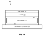
- FIG. 2B shows a cross-sectional diagram of a GaN based high power amplifier module 200 configured in accordance with an embodiment of the present invention.
- FIGS. 3A-C show a series of layout diagrams of GaN HPA MMICs utilizing an example NDPA circuit architecture, including the pre-driver, driver, and HPA designs, in accordance with an embodiment of the present invention.
- FIG. 4 is a plot of frequency (GHz) versus magnitude (dB) of small-signal performance of twelve GaN driver MMICs shown in FIG. 3B , in accordance with an embodiment of the present invention.
- FIG. 5 is a diagram of an example non-shared drain HPA 500 , configured in accordance with an embodiment of the present invention.
- FIG. 6 is a plot of the non-shared drain HPA 500 performance showing both frequency (GHz) versus power gain (dB) and frequency (GHz) versus the input/output power ratio (dBm), in accordance with an embodiment of the present invention.
- FIG. 7 is a diagram of a GaN HPA module 700 configured in accordance with an embodiment of the present invention.
- Some embodiments of the present invention may incorporate three elements into a solution for achieving a small form-factor solid-state High Power Amplifier (HPA). Such embodiments may produce smaller sized, high power EW transmitters not currently achievable with tube-based amplifier technology.
- the first of these elements employs the use of gallium nitride (GaN), a high-power-density semiconductor technology, capable of nearly a 10-fold increase in RF device output power over currently available gallium arsenic (GaAs) semiconductor technology.
- Dual field plate GaN transistors represent a wideband gap semiconductor technology that is suitable for operation up through 20 GHz and capable of providing a sufficiently high power density to achieve RF power levels comparable to those of TWTAs.
- GaN transistors operate at significantly lower voltages than TWTAs (e.g., 25 to 40 V), but are capable of achieving power densities that enable GaN transistors, appropriately combined, to provide comparable output power levels to those obtained from TWTAs.
- Some embodiments of the present invention that employ GaN transistors as TWTA replacements further provide sufficient thermal management in the package design to accommodate a high (e.g., 8-12 W/mm 2 ) power dissipation, and utilize a circuit architecture that can provide a wideband frequency performance and maintain a high-output power level.
- One example embodiment of the present invention integrates: (a) advanced GaN device technology, (b) wideband, distributed circuit architecture with Non-Uniformly Distributed Power Amplifier (NDPA), and (c) a thermal packaging approach employing advanced thermal management.
- NDPA Non-Uniformly Distributed Power Amplifier
- the combination of these elements offers a solution for the problem of achieving a small form-factor, solid-state replacement for wideband TWTAs.
- the first element involves the use of a dual field plate GaN device on a silicon carbide (SiC) substrate which provides a transistor technology that operates with sufficiently high power density to achieve output power levels comparable to TWTAs.
- a dual field plate GaN device on a silicon carbide (SiC) substrate which provides a transistor technology that operates with sufficiently high power density to achieve output power levels comparable to TWTAs.
- Currently available GaAs technology can provide RF power densities of only 1-2 W/mm. Achieving output power levels of, for instance, 50 to 100 watts, requires in excess of 25 to 50 mm of total device periphery, a non-realistic size for GaAs Monolithic Microwave Integrated Circuits (MMIC) technology.
- MMIC Microwave Integrated Circuits
- the use of GaN technology can provide, for instance, greater than 5 W/mm of output power density for realistic die area (e.g., 14-20 mm of device periphery).
- high levels of output power can be achieved using realizable die
- the second element of this specific example embodiment involves the use of a circuit architecture that is capable of multiple octaves of frequency performance critical for the wideband nature of many EW transmitter systems.
- NDPA circuit architecture in MMICs that integrate GaN based transistors, the required bandwidth performance typical of TWTAs can be achieved.
- the use of the NDPA architecture is not only advantageous for its wideband frequency performance, but the distributed nature of the NDPA topology facilitates the thermal management on the GaN die.
- the individual transistor heat-sources are more distributed than other more conventional MMIC amplifier architectures, and therefore, proximity heating of individual transistors contained on the MMIC is minimized.
- the third element of this specific example embodiment includes a thermal management technology that is employed in the amplifier package and allows high-power-density devices to be integrated into miniaturized packages, achieving acceptable electrical performance without the need for liquid or phase-change cooling approaches, in accordance with some such embodiments.
- a high thermal conductivity heat-spreader material such as a metallic coated Chemical Vapor Deposited (CVD) diamond material, is placed within the amplifier package beneath the GaN MMICs.
- the metallic coating may, for example, be gold or other electrically conductive material (e.g., silver, aluminum) or alloys thereof.
- the metallic coating may be applied to all sides of the packaging (e.g., top, bottom and four sides, assuming a square package, although other package shapes can be used as well) of the CVD diamond material with a thickness of, for example, about 6-12 micrometers in some such embodiments. Other thicknesses may also be used as will be appreciated in light of this disclosure, depending on factors such as the type of coating material (or materials) used and the conductivity of those material(s), and desired power levels.
- the coating material provides electrical conductivity and facilitates the thermal spreading in the high power dissipation environment of the small form-factor package and significantly reduces the operating junction temperature of the GaN devices, which in turn minimizes any performance degradation that may otherwise be exhibited in GaN devices at high temperature.
- the high thermal conductivity heat-spreader material (e.g., 1000 to 1800 W/(m° C.), in some example embodiments) may be incorporated, for instance, into the module flooring to provide improved thermal management for minimizing die junction temperature in the small form-factor amplifier package. Higher output power levels may be obtained from operation of the amplifier with shorter pulse widths. In some such example embodiments, providing such higher output power levels in a form-factor package may be achieved with additional or otherwise supplemental thermal management techniques beyond convection cooling in order to maintain the optimal power levels from the GaN MMICs.
- High-power-density GaN transistors embedded or otherwise formed into circuits that operate over broad frequency bandwidths and having these circuits integrated into small packages that are capable of managing a severe thermal environment provide a solid-state replacement for TWTAs.
- the described three elements provide the desired capability and enables solid-state HPAs that provide comparable performance to TWTAs without the cumbersome size and high-voltage power supply limitations of the tube-based approaches.
- Example embodiments of the invention have demonstrated a compact (e.g., 1.2 cubic-inches, although numerous other form-factors are possible as will be appreciated in light of this disclosure) TWTA-replacements for use in an EW frequency band.
- HEMTs High Electron Mobility Transistor
- the Maximum Stable Gain (MSG) as a function of frequency is shown in FIG. 1 for three 800 ⁇ m GaN HEMT discrete devices of varying gate lengths. While the difference in crossover frequency (frequency where the stability factor is above unity) is essentially the same, the gain for the 0.35 ⁇ m and the 0.5 ⁇ m device is 4 dB and 1 dB lower, respectively than the 0.25 ⁇ m device. From a fabrication point of view, the larger the gate length, the more simplified the fabrication tolerances and the higher the process yield.
- the device gate-width and critical channel dimensions were also evaluated using the structures on the discrete device mask set.
- Example transistor structures were included for the purposes of investigating gate width variation from 100 ⁇ m to 500 ⁇ m, gate pitch (i.e., gate-to-gate distance) variation from 50 ⁇ m to 70 ⁇ m, and drain-source spacing variation from 2 ⁇ m to 4 ⁇ m. The result from these studies was the selection of a more optimized transistor device structure suitable for a baseline GaN device in power amplifier MMIC applications to 10 GHz.
- the HPA can also be designed to satisfy desired application objectives, which in one example case include: (a) a nominal power gain of 45-50 dB, (b) a nominal output power level of 50 W, and (c) a bandwidth performance extending from 1-8 GHz.
- desired application objectives which in one example case include: (a) a nominal power gain of 45-50 dB, (b) a nominal output power level of 50 W, and (c) a bandwidth performance extending from 1-8 GHz.
- desired application objectives in one example case include: (a) a nominal power gain of 45-50 dB, (b) a nominal output power level of 50 W, and (c) a bandwidth performance extending from 1-8 GHz.
- desired application objectives which in one example case include: (a) a nominal power gain of 45-50 dB, (b) a nominal output power level of 50 W, and (c) a bandwidth performance extending from 1-8 GHz.
- MMIC based amplifier architecture was selected.
- the MMIC approach was selected for achieving the
- the resultant chipset included a pre-driver 202 , driver 204 , and several variants of the HPA 206 .
- the pre-driver 202 and driver 204 MMICs were designed to provide the desired gain and input drive level to the HPA 206 , and the HPA 206 was sized appropriately to achieve a nominal 50 W output power, in this example embodiment.
- the pre-driver 202 , driver 204 , and the HPA 206 utilize the prior discussed GaN amplifier MMIC design.
- Embodiments are not limited to the described pre-driver 202 , driver 204 , and the HPA 206 design as will be appreciated in light of the disclosure.
- Various additional stage drivers may be included, substituted, or omitted based on the desired output and other design considerations.
- the HPA 206 may be used without the pre-driver 202 and driver 204 .
- FIG. 2B a cross-sectional diagram of the high power amplifier module 200 is shown which is configured in accordance with one embodiment of the present invention.
- the amplification stages are implemented with GaN devices 208 , which may include the optional pre-driver 202 , the optional driver 204 , and HPA 206 (or a variant thereof, as will be appreciated in light of this disclosure), and are constructed on top of a substrate 210 .
- the substrate 210 may be constructed using, for example, SiC as previously discussed. Other suitable substrate materials can be used as well.
- the GaN, MMIC die or chipsets may each be coupled to the amplifier package housing 212 via a metallic coating material 214 of CVD diamond material 216 .
- the construction and thicknesses of the coating material 214 and the CVD diamond material 216 may be, for example, a metal coating of the CVD diamond as described herein.
- the metallic coating material 214 provides electrical conductivity and facilitates the thermal spreading in the high power dissipation environment of the small form-factor package and significantly reduces the operating junction temperature of the GaN devices 208 .
- the diamond 216 provides thermal conductivity to dissipate heat from die 208 .
- FIGS. 3A-C provides example device layout diagrams for the pre-driver 202 , driver 204 , and the HPA 206 , respectively.
- the cascade of GaN chips including a single-stage pre-driver 202 MMIC in FIG. 3A , a two-stage driver 204 MMIC in FIG. 3B , and a 19.2 mm total-gate-periphery HPA 206 MMIC in FIG. 3C .
- the single-stage pre-driver MMIC 202 incorporates a single-stage architecture with a 0.9 mm total gate-periphery stage.
- the pre-driver 202 includes a pre-driver input 302 supplying the amplifying signal to pre-driver GaN transistors 304 .
- the output of the pre-driver GaN transistors 304 is supplied from the pre-driver output 306 forward to the driver input 310 .
- biasing and impedance matching pre-driver circuitry 308 may also be provided on the pre-driver chip.
- the additional circuitry may include, for example, impedance networks, inductive and capacitive decoupling, and/or other signal conditioning circuitry.
- the two-stage driver MMIC 204 incorporates a two-stage architecture with a cascade of two 0.9 mm total gate-periphery stages.
- the amplifying signal is feed from the driver input 310 to the driver GaN transistors 312 having two stages in series each including three GaN transistors.
- the output of the driver GaN transistors 312 is supplied from the driver output 314 forward to the HPA driver input 316 .
- additional biasing and impedance matching driver circuitry 315 may also be provided on the driver chip.
- the example detailed embodiment of the HPA 206 shown in FIG. 3C uses NDPA circuit architecture using MMICs.
- the HPA 206 includes an HPA driver input 316 supplying the amplifying signal to a HPA driver portion 318 .
- the HPA driver portion 318 supplies the amplifying signal to the non-uniform distributed amplifier strings at the power stage 322 .
- the power stage 322 includes four strings, here labeled strings 324 A, 324 B, 324 C and 324 D.
- strings 324 A and 324 B the gate trace forms the divider and impedance transformer between the output of the HPA driver portion 318 and the input 320 to both strings 324 A and 324 B.
- the gate trace can be a stepped structure that steps the impedance on the gate electrodes from the first transistor 332 A to the last transistor 332 B, such that the associated inductance successively increases from input 320 to output 328 .
- the inductances formed by drain trace 326 form inductances between the transistors that successively decrease from input transistor 332 A to output transistor 332 B.
- Strings 324 A and 324 B have their outputs combined and share drain trace 326 , which functions to combine the outputs, to inject the drain bias, and to perform an impedance matching function.
- Strings 324 C and 324 D have a mirror structure and also function to combine outputs with strings 324 A and 324 B.
- FIG. 4 depicts the small-signal gain performance of the example two-stage driver 204 shown in FIG. 3B .
- the driver 204 exhibited a nominal 22 dB of small-signal gain over 2 octaves of frequency (2-8 GHz) when measured on-wafer, and 3 octaves of frequency performance when die-attached to a carrier with off-chip bias components.
- the bandwidth improvement was due to the fact that the lower frequency response of these MMICs is affected by the inductive loading of the DC probes used during the on-wafer measurements.
- the MMIC response extends down to 1 GHz, as designed.
- the single-stage pre-driver 202 MMIC was designed in a similar manner to the driver MMIC 204 using a single 0.9 mm total-gate-periphery GaN circuit.
- the pre-driver 202 achieved 12 dB of small-signal gain from 1 to 8 GHz.
- FIG. 5 illustrates another example of a non-shared drain HPA 500 that can be used in accordance with an embodiment of the present invention.
- the topology of the non-shared drain HPA 500 is a derivative of a distributed amplifier architecture which, in addition to its inherent wideband frequency performance, also facilities the thermal management of the module by distributing the heat sources of the devices more uniformly throughout the MMIC die area.
- the non-shared drain HPA 500 may be the same size as example HPA 206 to maintain compatibility in the high power amplifier module assembly, as described herein.
- the power stage 502 includes two strings, here labeled strings 504 A and 504 B. Similar to the previously described HPA 206 , the drain trace 506 A and 506 B are each a stepped structure that steps the impedance on the drain electrodes from the first transistor 512 A to the last transistor 512 B, such that the associated inductance successively decreases from input 510 to output 508 . Strings 504 A and 504 B have their outputs combined but unlike HPA 206 have individual drain traces 506 A and 506 B, which functions to combine the cell outputs, to inject the drain bias, and to perform an impedance matching function.
- the non-shared drain HPA 500 may use a 12 mm total-gate-periphery output stage with a 4.8 mm total-gate-periphery first-stage.
- the 2.5:1 drive ratio was used in this example design to provide sufficient drive power to the second-stage of the non-shared drain HPA 500 and to maintain the desired level of drive compression.
- the architecture of this chip utilized six 800 um cell devices in the first stage and ten 1.2 mm cell devices in the second stage.
- the chip size may be 6.831 mm ⁇ 4.958 mm.
- the on-wafer RF measurements of the non-shared drain HPA 500 is shown when driven 2 dB into compression at a drain voltage of 36 V and a gate voltage of ⁇ 1.8 V.
- An off-chip impedance matching circuit, fabricated on a dielectric substrate was used at the output of all the HPA MMICs to impedance-match the MMIC amplifier to 50 ohms.
- the non-shared drain HPA 500 of this example configuration achieved a nominal 40 watts of output power from 1 to 8 GHz when driven with 28 dBm input power (as will be appreciated, other test parameters such as input power, etc can be used, and the example provided here are not intended to imply limitations on the claimed invention).
- the nearly 34 mm 2 size of the GaN, MMIC HPA 206 and 500 was relatively large; however, the dc-yield of these designs was exceptionally good.
- the yield criteria were a simple pinch-off screen and a relatively benign on-state modulation current screen. Table 1 illustrates the results of this analysis.
- the first wafer was an iron doped buffer wafer and exhibited a dc-yield of 47% (24 out of 51).
- Another wafer was an aluminum gallium nitride AlGaN doped buffer wafer and exhibited a dc-yield of 76% (39 out of 51). Large MMICs that pass this dc-screen have shown excellent correlation with RF functioning die when full on-wafer RF evaluation is not practical.
- an HPA module 700 provided a GaN amplifier packaging that resulted in a module having an RF input 702 and RF output 704 with a total volume of 1.2 cubic-inches, in accordance with one example embodiment of the present invention. Contained within this volume is a cascade of three GaN MMIC chips including a single-stage pre-driver MMIC 202 , the two-stage driver MMIC 206 , and the 19.2 mm total-gate-periphery HPA MMIC 206 , as well as bias conditioning circuitry 706 controlled by DC and control inputs 708 .
- the bias conditioning circuitry 706 may be capable of supporting pulsed gate or drain bias.
- bias conditioning circuitry 706 enabled the application of two bipolar bias voltage ports, one for the negative gate bias and one for the higher-current drain bias. Bias filtering and voltage stability was also addressed by this bias conditioning circuitry 706 . In addition to the off-chip matching network at the output of the HPA, off-chip bias components were also incorporated along each side of the GaN MMICs to facilitate MMIC biasing.
- the HPA modules 700 may provide a small form-factor amplifier package.
- the thermal management strategy employed can also consider the vicinity of the HPA 206 sub-assembly to minimize performance degradation due to die temperature. This may include, for example, the use of high thermal conductivity materials beneath the GaN HPA MMIC 206 , as previously described.
- a total of five stages of amplifier gain are utilized in what is essentially a single transmit channel amplifier module.
- the resulting example amplifier provided a nominal 45 dB of power gain.
- the final stage was operated at 3 to 4 dB of gain compression where the output power ranged from 25 to 50 watts over the 1 to 8 GHz frequency bandwidth.
- the measured output power versus frequency performance of the HPA module 700 for a 10% duty cycle operation is provided.
- the output power versus input power for three frequencies using a shorter pulse width of 2 ⁇ sec is also provided.
- the average output power was 40 W over the 1 to 8 GHz bandwidth.
- an output power of greater than 70 W was measured.
- a wideband GaN on SiC amplifier MMIC chip set (pre-driver 202 , driver 204 , and the HPA 206 ) has been described for use in compact HPA modules 700 using small form-factor packages.
- a combination of elements including dual field plate GaN semiconductor technology on silicon carbide substrate, a non-uniform distributed form of MMIC amplifier architecture, and advanced thermal management in the package design a peak output power of 70 W with an average output power of 40 W was demonstrated by this 1.2 in 3 HPA amplifier module 700 .
- the amplifier module 700 has demonstrated the feasibility of replacing tube-based transmitter technology with compact high-power solid-state technology having reduced size and weight as compared with tube-based amplifiers.
Landscapes
- Engineering & Computer Science (AREA)
- Microelectronics & Electronic Packaging (AREA)
- Power Engineering (AREA)
- Amplifiers (AREA)
- Microwave Amplifiers (AREA)
Abstract
Description
| TABLE I |
| DC-Yield of Large-Periphery GaN HPA MMICs from two 3-inch wafers |
| DC Yields |
| Sites/ | |||||
| 07029w2 | 07029w3 | Wafer | Periphery | ||
| Full output | D295-4 | 4 | 9 | 12 | 4.8/14.4-mm |
| chips | D295-5 | 5 | 9 | 13 | 4.8/9.6-mm |
| D295-7 | 9 | 9 | 13 | 4.8/12.0- | |
| Total | |||||
| 18 | 27 | 38 | |||
| Half output | D295-6 | 6 | 12 | 13 | 1.6/5.6-mm |
| chip | |||||
Claims (21)
Priority Applications (3)
| Application Number | Priority Date | Filing Date | Title |
|---|---|---|---|
| US13/016,599 US8669812B2 (en) | 2004-11-23 | 2011-01-28 | High power amplifier |
| US13/081,279 US8076975B1 (en) | 2004-11-23 | 2011-04-06 | Broadband high power amplifier |
| US13/316,900 US8576009B2 (en) | 2004-11-23 | 2011-12-12 | Broadband high power amplifier |
Applications Claiming Priority (5)
| Application Number | Priority Date | Filing Date | Title |
|---|---|---|---|
| US63034304P | 2004-11-23 | 2004-11-23 | |
| PCT/US2005/039407 WO2006057774A2 (en) | 2004-11-23 | 2005-11-01 | Solid-state ultra-wideband microwave power amplifier employing modular non-uniform distributed amplifier elements |
| US62902506A | 2006-12-08 | 2006-12-08 | |
| US29907210P | 2010-01-28 | 2010-01-28 | |
| US13/016,599 US8669812B2 (en) | 2004-11-23 | 2011-01-28 | High power amplifier |
Related Parent Applications (3)
| Application Number | Title | Priority Date | Filing Date |
|---|---|---|---|
| US11/629,025 Continuation-In-Part US7924097B2 (en) | 2004-11-23 | 2005-11-01 | Solid-state ultra-wideband microwave power amplifier employing modular non-uniform distributed amplifier elements |
| PCT/US2005/039407 Continuation-In-Part WO2006057774A2 (en) | 2004-11-23 | 2005-11-01 | Solid-state ultra-wideband microwave power amplifier employing modular non-uniform distributed amplifier elements |
| US62902506A Continuation-In-Part | 2004-11-23 | 2006-12-08 |
Related Child Applications (1)
| Application Number | Title | Priority Date | Filing Date |
|---|---|---|---|
| US13/081,279 Continuation-In-Part US8076975B1 (en) | 2004-11-23 | 2011-04-06 | Broadband high power amplifier |
Publications (2)
| Publication Number | Publication Date |
|---|---|
| US20120268213A1 US20120268213A1 (en) | 2012-10-25 |
| US8669812B2 true US8669812B2 (en) | 2014-03-11 |
Family
ID=47020853
Family Applications (1)
| Application Number | Title | Priority Date | Filing Date |
|---|---|---|---|
| US13/016,599 Expired - Fee Related US8669812B2 (en) | 2004-11-23 | 2011-01-28 | High power amplifier |
Country Status (1)
| Country | Link |
|---|---|
| US (1) | US8669812B2 (en) |
Cited By (2)
| Publication number | Priority date | Publication date | Assignee | Title |
|---|---|---|---|---|
| US9742445B1 (en) | 2016-07-01 | 2017-08-22 | Bae Systems Information And Electronic Systems Integration Inc. | High power radio frequency amplifier architecture |
| US20220231640A1 (en) * | 2020-12-30 | 2022-07-21 | Skyworks Solutions, Inc. | Power amplifier having analog pre-distortion by adaptive degenerative feedback |
Families Citing this family (5)
| Publication number | Priority date | Publication date | Assignee | Title |
|---|---|---|---|---|
| US9537605B1 (en) * | 2014-07-22 | 2017-01-03 | Bae Systems Information And Electronic Systems Integration Inc. | Ultra-wideband high-power solid-state transmitter for electronic warfare applications |
| US9899970B2 (en) * | 2015-06-18 | 2018-02-20 | Eridan Communications, Inc. | Current enhanced driver for high-power solid-state radio frequency power amplifiers |
| US11159134B2 (en) * | 2019-12-19 | 2021-10-26 | Nxp Usa, Inc. | Multiple-stage power amplifiers and amplifier arrays configured to operate using the same output bias voltage |
| US11522508B1 (en) | 2021-08-13 | 2022-12-06 | Raytheon Company | Dual-band monolithic microwave IC (MMIC) power amplifier |
| EP4325721A4 (en) * | 2022-04-28 | 2024-08-07 | Suzhou Watech Electronics Co., Ltd. | Package structure for signal amplification, and signal amplifier |
Citations (28)
| Publication number | Priority date | Publication date | Assignee | Title |
|---|---|---|---|---|
| US4486719A (en) | 1982-07-01 | 1984-12-04 | Raytheon Company | Distributed amplifier |
| US4540954A (en) * | 1982-11-24 | 1985-09-10 | Rockwell International Corporation | Singly terminated distributed amplifier |
| US4543535A (en) | 1984-04-16 | 1985-09-24 | Raytheon Company | Distributed power amplifier |
| US4733195A (en) | 1986-07-15 | 1988-03-22 | Texas Instruments Incorporated | Travelling-wave microwave device |
| US4754234A (en) | 1986-02-28 | 1988-06-28 | U.S. Philips Corporation | Broadband distributed amplifier for microwave frequences |
| US4788511A (en) | 1987-11-30 | 1988-11-29 | Raytheon Company | Distributed power amplifier |
| US5021743A (en) * | 1989-11-30 | 1991-06-04 | Raytheon Company | Biasing networks for matrix amplifiers |
| US5028879A (en) | 1984-05-24 | 1991-07-02 | Texas Instruments Incorporated | Compensation of the gate loading loss for travelling wave power amplifiers |
| US5046155A (en) | 1990-04-06 | 1991-09-03 | Wisconsin Alumni Research Foundation | Highly directive, broadband, bidirectional distributed amplifier |
| US5168242A (en) * | 1991-11-20 | 1992-12-01 | Itt Corporation | Active-type broadband power divider |
| US5177381A (en) * | 1991-12-06 | 1993-01-05 | Motorola, Inc. | Distributed logarithmic amplifier and method |
| US5361038A (en) * | 1993-03-11 | 1994-11-01 | Trw Inc. | Active load applications for distributed circuits |
| US5414387A (en) * | 1993-07-14 | 1995-05-09 | Mitsubishi Denki Kabushiki Kaisha | Distributed amplifier and bidirectional amplifier |
| US5469108A (en) * | 1994-08-15 | 1995-11-21 | Texas Instruments Incorporated | Reactively compensated power transistor circuits |
| US5485118A (en) | 1994-06-03 | 1996-01-16 | Massachusetts Institute Of Technology | Non-uniformly distributed power amplifier |
| US5801591A (en) | 1997-05-13 | 1998-09-01 | Verticom, Inc. | Microwave linear oscillator/amplifier utilizing a multicoupled ferrite resonator |
| US5986518A (en) * | 1998-06-30 | 1999-11-16 | Motorola, Inc. | Distributed MMIC active quadrature hybrid and method for providing in-phase and quadrature-phase signals |
| US6215360B1 (en) * | 1998-02-23 | 2001-04-10 | Motorola, Inc. | Semiconductor chip for RF transceiver and power output circuit therefor |
| US6252461B1 (en) | 1997-08-25 | 2001-06-26 | Frederick Herbert Raab | Technique for wideband operation of power amplifiers |
| US6538509B2 (en) | 2001-03-09 | 2003-03-25 | Dragonwave Inc. | Linearizer for a power amplifier |
| US20030231061A1 (en) | 2000-12-27 | 2003-12-18 | Lautzenhiser Barry Arthur | Divided-voltage FET power amplifiers |
| US6674329B1 (en) | 2002-06-27 | 2004-01-06 | Motorola, Inc. | Distributed RF amplifier with filtered dummy load |
| US6791417B2 (en) | 2002-01-28 | 2004-09-14 | Cree Microwave, Inc. | N-way RF power amplifier circuit with increased back-off capability and power added efficiency using selected phase lengths and output impedances |
| US6798281B2 (en) * | 2001-12-18 | 2004-09-28 | Thales | Two-input/two-output broadband active selector switch with distributed structure, and phase control device comprising such a switch |
| US6900695B2 (en) * | 2000-11-20 | 2005-05-31 | Totalforsvarets Forskningsinstitut | Reconfigurable broadband active power splitter ditto power combiner and ditto bidirectional power splitter/power combiner and circuits based on these |
| US20080090539A1 (en) | 2006-10-11 | 2008-04-17 | Thompson Rick L | Fuzzy logic control of an RF power amplifier for automatic self-tuning |
| US7688135B2 (en) * | 2007-04-23 | 2010-03-30 | Dali Systems Co. Ltd. | N-way Doherty distributed power amplifier |
| US8058930B1 (en) * | 2009-01-02 | 2011-11-15 | Rf Micro Devices, Inc. | Capacitively-coupled non-uniformly distributed amplifier |
-
2011
- 2011-01-28 US US13/016,599 patent/US8669812B2/en not_active Expired - Fee Related
Patent Citations (29)
| Publication number | Priority date | Publication date | Assignee | Title |
|---|---|---|---|---|
| US4486719A (en) | 1982-07-01 | 1984-12-04 | Raytheon Company | Distributed amplifier |
| US4540954A (en) * | 1982-11-24 | 1985-09-10 | Rockwell International Corporation | Singly terminated distributed amplifier |
| US4543535A (en) | 1984-04-16 | 1985-09-24 | Raytheon Company | Distributed power amplifier |
| US5028879A (en) | 1984-05-24 | 1991-07-02 | Texas Instruments Incorporated | Compensation of the gate loading loss for travelling wave power amplifiers |
| US4754234A (en) | 1986-02-28 | 1988-06-28 | U.S. Philips Corporation | Broadband distributed amplifier for microwave frequences |
| US4733195A (en) | 1986-07-15 | 1988-03-22 | Texas Instruments Incorporated | Travelling-wave microwave device |
| US4788511A (en) | 1987-11-30 | 1988-11-29 | Raytheon Company | Distributed power amplifier |
| US5021743A (en) * | 1989-11-30 | 1991-06-04 | Raytheon Company | Biasing networks for matrix amplifiers |
| US5046155A (en) | 1990-04-06 | 1991-09-03 | Wisconsin Alumni Research Foundation | Highly directive, broadband, bidirectional distributed amplifier |
| US5168242A (en) * | 1991-11-20 | 1992-12-01 | Itt Corporation | Active-type broadband power divider |
| US5177381A (en) * | 1991-12-06 | 1993-01-05 | Motorola, Inc. | Distributed logarithmic amplifier and method |
| US5361038A (en) * | 1993-03-11 | 1994-11-01 | Trw Inc. | Active load applications for distributed circuits |
| US5414387A (en) * | 1993-07-14 | 1995-05-09 | Mitsubishi Denki Kabushiki Kaisha | Distributed amplifier and bidirectional amplifier |
| US5485118A (en) | 1994-06-03 | 1996-01-16 | Massachusetts Institute Of Technology | Non-uniformly distributed power amplifier |
| US5469108A (en) * | 1994-08-15 | 1995-11-21 | Texas Instruments Incorporated | Reactively compensated power transistor circuits |
| US5801591A (en) | 1997-05-13 | 1998-09-01 | Verticom, Inc. | Microwave linear oscillator/amplifier utilizing a multicoupled ferrite resonator |
| US6252461B1 (en) | 1997-08-25 | 2001-06-26 | Frederick Herbert Raab | Technique for wideband operation of power amplifiers |
| US6552634B1 (en) | 1997-08-25 | 2003-04-22 | Frederick Herbert Raab | Wideband, minimum-rating filters and multicouplers for power amplifiers |
| US6215360B1 (en) * | 1998-02-23 | 2001-04-10 | Motorola, Inc. | Semiconductor chip for RF transceiver and power output circuit therefor |
| US5986518A (en) * | 1998-06-30 | 1999-11-16 | Motorola, Inc. | Distributed MMIC active quadrature hybrid and method for providing in-phase and quadrature-phase signals |
| US6900695B2 (en) * | 2000-11-20 | 2005-05-31 | Totalforsvarets Forskningsinstitut | Reconfigurable broadband active power splitter ditto power combiner and ditto bidirectional power splitter/power combiner and circuits based on these |
| US20030231061A1 (en) | 2000-12-27 | 2003-12-18 | Lautzenhiser Barry Arthur | Divided-voltage FET power amplifiers |
| US6538509B2 (en) | 2001-03-09 | 2003-03-25 | Dragonwave Inc. | Linearizer for a power amplifier |
| US6798281B2 (en) * | 2001-12-18 | 2004-09-28 | Thales | Two-input/two-output broadband active selector switch with distributed structure, and phase control device comprising such a switch |
| US6791417B2 (en) | 2002-01-28 | 2004-09-14 | Cree Microwave, Inc. | N-way RF power amplifier circuit with increased back-off capability and power added efficiency using selected phase lengths and output impedances |
| US6674329B1 (en) | 2002-06-27 | 2004-01-06 | Motorola, Inc. | Distributed RF amplifier with filtered dummy load |
| US20080090539A1 (en) | 2006-10-11 | 2008-04-17 | Thompson Rick L | Fuzzy logic control of an RF power amplifier for automatic self-tuning |
| US7688135B2 (en) * | 2007-04-23 | 2010-03-30 | Dali Systems Co. Ltd. | N-way Doherty distributed power amplifier |
| US8058930B1 (en) * | 2009-01-02 | 2011-11-15 | Rf Micro Devices, Inc. | Capacitively-coupled non-uniformly distributed amplifier |
Non-Patent Citations (6)
| Title |
|---|
| International Report on Patentability with Written Opinion of the International Searching Authority, received in International Patent Application No. PCT/US05/39407, 7 pgs. |
| International Search Report, dated Aug. 10, 2006, received in International Patent Application No. PCT/US05/39407, 4 pgs. |
| Notice of Allowance dated Dec. 9, 2010 in U.S. Patent Publication No. US 2009-0309659, 6 pages. |
| Notice of Allowance dated Oct. 26, 2011 in U.S. Appl. No. 13/081,279, 7 pages. |
| Office Action Response filed Nov. 18, 2010 in U.S. Patent Publication No. US 2009-0309659, 8 pages. |
| Office Action Response filed Oct. 19, 2011 in U.S. Appl. No. 13/081,279, 4 pages. |
Cited By (3)
| Publication number | Priority date | Publication date | Assignee | Title |
|---|---|---|---|---|
| US9742445B1 (en) | 2016-07-01 | 2017-08-22 | Bae Systems Information And Electronic Systems Integration Inc. | High power radio frequency amplifier architecture |
| US20220231640A1 (en) * | 2020-12-30 | 2022-07-21 | Skyworks Solutions, Inc. | Power amplifier having analog pre-distortion by adaptive degenerative feedback |
| US12224716B2 (en) * | 2020-12-30 | 2025-02-11 | Skyworks Solutions, Inc. | Power amplifier having analog pre-distortion by adaptive degenerative feedback |
Also Published As
| Publication number | Publication date |
|---|---|
| US20120268213A1 (en) | 2012-10-25 |
Similar Documents
| Publication | Publication Date | Title |
|---|---|---|
| US8669812B2 (en) | High power amplifier | |
| US11515842B2 (en) | Doherty power amplifiers and devices with low voltage driver stage in carrier-path and high voltage driver stage in peaking-path | |
| JP2019087992A (en) | Multiple-stage power amplifiers implemented with multiple semiconductor technologies | |
| Shin et al. | X-band GaN MMIC power amplifier for the SSPA of a SAR system | |
| US12519426B2 (en) | Integrated power amplifier with bias control and harmonic termination | |
| Noh et al. | Highly integrated C-band GaN high power amplifier MMIC for phased array applications | |
| Kanaya et al. | A Ku-band 20 W GaN-MMIC amplifier with built-in linearizer | |
| Micovic et al. | GaN mmic pas for e-band (71 ghz-95 ghz) radio | |
| Dennler et al. | Monolithic three-stage 6–18GHz high power amplifier with distributed interstage in GaN technology | |
| Chen et al. | A compact 70 watt power amplifier MMIC utilizing S-band GaN on SiC HEMT process | |
| Komiak et al. | Fully monolithic 4 watt high efficiency Ka-band power amplifier | |
| US20220182022A1 (en) | Power amplifier with a power transistor and an electrostatic discharge protection circuit on separate substrates | |
| Brown et al. | Millimeter wave GaN MMIC technologies for next-gen defense applications | |
| Noh et al. | A 16 watt X-band GaN high power amplifier MMIC for phased array applications | |
| Torii et al. | 44 dBm output power and high gain K-band GaN power amplifier for satellite communication | |
| Chen et al. | A high efficiency 4–18 GHz GaN MMIC power amplifier based on 90nm T-gate GaN HEMT technology | |
| Nakatani et al. | Ka-band high efficiency and high linearity GaN power amplifiers for broadband high throughput satellite communication systems | |
| Imran et al. | GaN HEMT based Ku-band power amplifier MMIC | |
| Friesicke et al. | V-band GaN power amplifier MMICs with high power-bandwidth and low gain compression for RF inter-satellite links | |
| Dennler et al. | Novel semi-reactively-matched multistage broadband power amplifier architecture for monolithic ICs in GaN technology | |
| Komiak | Wideband power amplifiers-1948 to the present day | |
| Bosch et al. | Low cost X-band power amplifier MMIC fabricated on a 0.25/spl mu/m GaAs pHEMT process | |
| US12191813B2 (en) | Compact single stage wideband power amplifier | |
| Schuh et al. | X-band T/R-module front-end based on GaN MMICs | |
| Liu et al. | UHF-Band 4kW Broadband High Efficiency GaN Amplifier |
Legal Events
| Date | Code | Title | Description |
|---|---|---|---|
| AS | Assignment |
Owner name: BAE SYSTEMS INFORMATION AND ELECTRONIC SYSTEMS INT Free format text: ASSIGNMENT OF ASSIGNORS INTEREST;ASSIGNORS:ACTIS, ROBERT;LENDER, ROBERT J., JR.;RAJKOWSKI, STEVE M.;AND OTHERS;SIGNING DATES FROM 20110207 TO 20110208;REEL/FRAME:026343/0971 |
|
| AS | Assignment |
Owner name: SCHILMASS CO. L.L.C., DELAWARE Free format text: ASSIGNMENT OF ASSIGNORS INTEREST;ASSIGNOR:BAE SYSTEMS INFORMATION AND ELECTRONIC SYSTEMS INTEGRATION, INC.;REEL/FRAME:027606/0657 Effective date: 20111104 |
|
| STCF | Information on status: patent grant |
Free format text: PATENTED CASE |
|
| AS | Assignment |
Owner name: GULA CONSULTING LIMITED LIABILITY COMPANY, DELAWARE Free format text: MERGER;ASSIGNOR:SCHILMASS CO. L.L.C.;REEL/FRAME:037559/0856 Effective date: 20150826 Owner name: GULA CONSULTING LIMITED LIABILITY COMPANY, DELAWAR Free format text: MERGER;ASSIGNOR:SCHILMASS CO. L.L.C.;REEL/FRAME:037559/0856 Effective date: 20150826 |
|
| MAFP | Maintenance fee payment |
Free format text: PAYMENT OF MAINTENANCE FEE, 4TH YEAR, LARGE ENTITY (ORIGINAL EVENT CODE: M1551) Year of fee payment: 4 |
|
| MAFP | Maintenance fee payment |
Free format text: PAYMENT OF MAINTENANCE FEE, 8TH YEAR, LARGE ENTITY (ORIGINAL EVENT CODE: M1552); ENTITY STATUS OF PATENT OWNER: LARGE ENTITY Year of fee payment: 8 |
|
| FEPP | Fee payment procedure |
Free format text: MAINTENANCE FEE REMINDER MAILED (ORIGINAL EVENT CODE: REM.); ENTITY STATUS OF PATENT OWNER: LARGE ENTITY |
|
| LAPS | Lapse for failure to pay maintenance fees |
Free format text: PATENT EXPIRED FOR FAILURE TO PAY MAINTENANCE FEES (ORIGINAL EVENT CODE: EXP.); ENTITY STATUS OF PATENT OWNER: LARGE ENTITY |
|
| STCH | Information on status: patent discontinuation |
Free format text: PATENT EXPIRED DUE TO NONPAYMENT OF MAINTENANCE FEES UNDER 37 CFR 1.362 |