EP3479409B1 - Optoelectronic device comprising three-dimensional diodes - Google Patents
Optoelectronic device comprising three-dimensional diodes Download PDFInfo
- Publication number
- EP3479409B1 EP3479409B1 EP17742491.8A EP17742491A EP3479409B1 EP 3479409 B1 EP3479409 B1 EP 3479409B1 EP 17742491 A EP17742491 A EP 17742491A EP 3479409 B1 EP3479409 B1 EP 3479409B1
- Authority
- EP
- European Patent Office
- Prior art keywords
- nucleation
- diodes
- conductive
- optoelectronic device
- insulating layer
- Prior art date
- Legal status (The legal status is an assumption and is not a legal conclusion. Google has not performed a legal analysis and makes no representation as to the accuracy of the status listed.)
- Active
Links
- 230000005693 optoelectronics Effects 0.000 title claims description 57
- 230000006911 nucleation Effects 0.000 claims description 143
- 238000010899 nucleation Methods 0.000 claims description 143
- 239000000463 material Substances 0.000 claims description 124
- 239000000758 substrate Substances 0.000 claims description 50
- 230000012010 growth Effects 0.000 claims description 38
- 150000001875 compounds Chemical class 0.000 claims description 28
- 239000004020 conductor Substances 0.000 claims description 23
- 239000004065 semiconductor Substances 0.000 claims description 19
- 229910052723 transition metal Inorganic materials 0.000 claims description 18
- 229910052782 aluminium Inorganic materials 0.000 claims description 16
- XAGFODPZIPBFFR-UHFFFAOYSA-N aluminium Chemical compound [Al] XAGFODPZIPBFFR-UHFFFAOYSA-N 0.000 claims description 16
- 229910052735 hafnium Inorganic materials 0.000 claims description 15
- VBJZVLUMGGDVMO-UHFFFAOYSA-N hafnium atom Chemical compound [Hf] VBJZVLUMGGDVMO-UHFFFAOYSA-N 0.000 claims description 15
- 150000003624 transition metals Chemical class 0.000 claims description 15
- 229910002601 GaN Inorganic materials 0.000 claims description 14
- QCWXUUIWCKQGHC-UHFFFAOYSA-N Zirconium Chemical compound [Zr] QCWXUUIWCKQGHC-UHFFFAOYSA-N 0.000 claims description 13
- 239000003989 dielectric material Substances 0.000 claims description 13
- 239000010955 niobium Substances 0.000 claims description 13
- 229910052726 zirconium Inorganic materials 0.000 claims description 13
- 229910052758 niobium Inorganic materials 0.000 claims description 12
- GUCVJGMIXFAOAE-UHFFFAOYSA-N niobium atom Chemical compound [Nb] GUCVJGMIXFAOAE-UHFFFAOYSA-N 0.000 claims description 12
- 230000000284 resting effect Effects 0.000 claims description 12
- 229910052715 tantalum Inorganic materials 0.000 claims description 12
- GUVRBAGPIYLISA-UHFFFAOYSA-N tantalum atom Chemical compound [Ta] GUVRBAGPIYLISA-UHFFFAOYSA-N 0.000 claims description 12
- 229910052751 metal Inorganic materials 0.000 claims description 11
- 239000002184 metal Substances 0.000 claims description 11
- 150000004767 nitrides Chemical class 0.000 claims description 11
- 239000010936 titanium Substances 0.000 claims description 10
- 229910052720 vanadium Inorganic materials 0.000 claims description 10
- RTAQQCXQSZGOHL-UHFFFAOYSA-N Titanium Chemical compound [Ti] RTAQQCXQSZGOHL-UHFFFAOYSA-N 0.000 claims description 9
- 239000011651 chromium Substances 0.000 claims description 9
- 230000010287 polarization Effects 0.000 claims description 9
- 229910052719 titanium Inorganic materials 0.000 claims description 9
- VYZAMTAEIAYCRO-UHFFFAOYSA-N Chromium Chemical compound [Cr] VYZAMTAEIAYCRO-UHFFFAOYSA-N 0.000 claims description 8
- ZOKXTWBITQBERF-UHFFFAOYSA-N Molybdenum Chemical compound [Mo] ZOKXTWBITQBERF-UHFFFAOYSA-N 0.000 claims description 8
- 229910052804 chromium Inorganic materials 0.000 claims description 8
- 238000004519 manufacturing process Methods 0.000 claims description 8
- 229910052750 molybdenum Inorganic materials 0.000 claims description 8
- 239000011733 molybdenum Substances 0.000 claims description 8
- 238000004544 sputter deposition Methods 0.000 claims description 7
- WFKWXMTUELFFGS-UHFFFAOYSA-N tungsten Chemical compound [W] WFKWXMTUELFFGS-UHFFFAOYSA-N 0.000 claims description 7
- 229910052721 tungsten Inorganic materials 0.000 claims description 7
- 239000010937 tungsten Substances 0.000 claims description 7
- PMHQVHHXPFUNSP-UHFFFAOYSA-M copper(1+);methylsulfanylmethane;bromide Chemical compound Br[Cu].CSC PMHQVHHXPFUNSP-UHFFFAOYSA-M 0.000 claims description 5
- JMASRVWKEDWRBT-UHFFFAOYSA-N Gallium nitride Chemical group [Ga]#N JMASRVWKEDWRBT-UHFFFAOYSA-N 0.000 claims description 4
- FYYHWMGAXLPEAU-UHFFFAOYSA-N Magnesium Chemical compound [Mg] FYYHWMGAXLPEAU-UHFFFAOYSA-N 0.000 claims description 3
- 229910052749 magnesium Inorganic materials 0.000 claims description 3
- 239000011777 magnesium Substances 0.000 claims description 3
- GPPXJZIENCGNKB-UHFFFAOYSA-N vanadium Chemical compound [V]#[V] GPPXJZIENCGNKB-UHFFFAOYSA-N 0.000 claims 2
- 229910021480 group 4 element Inorganic materials 0.000 claims 1
- 239000013078 crystal Substances 0.000 description 35
- VYPSYNLAJGMNEJ-UHFFFAOYSA-N Silicium dioxide Chemical compound O=[Si]=O VYPSYNLAJGMNEJ-UHFFFAOYSA-N 0.000 description 23
- 230000005855 radiation Effects 0.000 description 14
- 229910052710 silicon Inorganic materials 0.000 description 12
- 229910052727 yttrium Inorganic materials 0.000 description 12
- 229910052581 Si3N4 Inorganic materials 0.000 description 11
- XUIMIQQOPSSXEZ-UHFFFAOYSA-N Silicon Chemical compound [Si] XUIMIQQOPSSXEZ-UHFFFAOYSA-N 0.000 description 11
- 239000010703 silicon Substances 0.000 description 11
- 239000002178 crystalline material Substances 0.000 description 10
- 230000004888 barrier function Effects 0.000 description 8
- 229910052681 coesite Inorganic materials 0.000 description 8
- 229910052906 cristobalite Inorganic materials 0.000 description 8
- 239000000377 silicon dioxide Substances 0.000 description 8
- 235000012239 silicon dioxide Nutrition 0.000 description 8
- 229910052682 stishovite Inorganic materials 0.000 description 8
- 229910052905 tridymite Inorganic materials 0.000 description 8
- LEONUFNNVUYDNQ-UHFFFAOYSA-N vanadium atom Chemical compound [V] LEONUFNNVUYDNQ-UHFFFAOYSA-N 0.000 description 8
- 238000005530 etching Methods 0.000 description 7
- 230000003287 optical effect Effects 0.000 description 7
- HQVNEWCFYHHQES-UHFFFAOYSA-N silicon nitride Chemical compound N12[Si]34N5[Si]62N3[Si]51N64 HQVNEWCFYHHQES-UHFFFAOYSA-N 0.000 description 7
- 229910052814 silicon oxide Inorganic materials 0.000 description 7
- QGZKDVFQNNGYKY-UHFFFAOYSA-N Ammonia Chemical compound N QGZKDVFQNNGYKY-UHFFFAOYSA-N 0.000 description 6
- GYHNNYVSQQEPJS-UHFFFAOYSA-N Gallium Chemical compound [Ga] GYHNNYVSQQEPJS-UHFFFAOYSA-N 0.000 description 6
- XLOMVQKBTHCTTD-UHFFFAOYSA-N Zinc monoxide Chemical compound [Zn]=O XLOMVQKBTHCTTD-UHFFFAOYSA-N 0.000 description 6
- 229910052733 gallium Inorganic materials 0.000 description 6
- 238000000034 method Methods 0.000 description 6
- 238000000137 annealing Methods 0.000 description 5
- 238000005538 encapsulation Methods 0.000 description 5
- 238000000407 epitaxy Methods 0.000 description 5
- PCHJSUWPFVWCPO-UHFFFAOYSA-N gold Chemical compound [Au] PCHJSUWPFVWCPO-UHFFFAOYSA-N 0.000 description 5
- 229910052737 gold Inorganic materials 0.000 description 5
- 239000010931 gold Substances 0.000 description 5
- -1 GaN Chemical class 0.000 description 4
- BLOIXGFLXPCOGW-UHFFFAOYSA-N [Ti].[Sn] Chemical compound [Ti].[Sn] BLOIXGFLXPCOGW-UHFFFAOYSA-N 0.000 description 4
- PNEYBMLMFCGWSK-UHFFFAOYSA-N aluminium oxide Inorganic materials [O-2].[O-2].[O-2].[Al+3].[Al+3] PNEYBMLMFCGWSK-UHFFFAOYSA-N 0.000 description 4
- 230000008901 benefit Effects 0.000 description 4
- 230000015572 biosynthetic process Effects 0.000 description 4
- 229910052593 corundum Inorganic materials 0.000 description 4
- 238000002425 crystallisation Methods 0.000 description 4
- 230000008025 crystallization Effects 0.000 description 4
- 229910052738 indium Inorganic materials 0.000 description 4
- APFVFJFRJDLVQX-UHFFFAOYSA-N indium atom Chemical compound [In] APFVFJFRJDLVQX-UHFFFAOYSA-N 0.000 description 4
- 238000002488 metal-organic chemical vapour deposition Methods 0.000 description 4
- 229910001845 yogo sapphire Inorganic materials 0.000 description 4
- IJGRMHOSHXDMSA-UHFFFAOYSA-N Atomic nitrogen Chemical compound N#N IJGRMHOSHXDMSA-UHFFFAOYSA-N 0.000 description 3
- RYGMFSIKBFXOCR-UHFFFAOYSA-N Copper Chemical compound [Cu] RYGMFSIKBFXOCR-UHFFFAOYSA-N 0.000 description 3
- 229910004205 SiNX Inorganic materials 0.000 description 3
- 229910020286 SiOxNy Inorganic materials 0.000 description 3
- BQCADISMDOOEFD-UHFFFAOYSA-N Silver Chemical compound [Ag] BQCADISMDOOEFD-UHFFFAOYSA-N 0.000 description 3
- 238000005229 chemical vapour deposition Methods 0.000 description 3
- 229910052802 copper Inorganic materials 0.000 description 3
- 239000010949 copper Substances 0.000 description 3
- 238000000151 deposition Methods 0.000 description 3
- 238000009396 hybridization Methods 0.000 description 3
- 239000011159 matrix material Substances 0.000 description 3
- 150000001247 metal acetylides Chemical class 0.000 description 3
- 229910052709 silver Inorganic materials 0.000 description 3
- 239000004332 silver Substances 0.000 description 3
- 239000011787 zinc oxide Substances 0.000 description 3
- 229910002704 AlGaN Inorganic materials 0.000 description 2
- 229910021529 ammonia Inorganic materials 0.000 description 2
- 238000000231 atomic layer deposition Methods 0.000 description 2
- 238000003877 atomic layer epitaxy Methods 0.000 description 2
- NWAIGJYBQQYSPW-UHFFFAOYSA-N azanylidyneindigane Chemical compound [In]#N NWAIGJYBQQYSPW-UHFFFAOYSA-N 0.000 description 2
- 230000000903 blocking effect Effects 0.000 description 2
- 229910052799 carbon Inorganic materials 0.000 description 2
- 230000001419 dependent effect Effects 0.000 description 2
- 230000008021 deposition Effects 0.000 description 2
- 238000010292 electrical insulation Methods 0.000 description 2
- 230000008030 elimination Effects 0.000 description 2
- 238000003379 elimination reaction Methods 0.000 description 2
- 230000004907 flux Effects 0.000 description 2
- 229910052732 germanium Inorganic materials 0.000 description 2
- 238000002248 hydride vapour-phase epitaxy Methods 0.000 description 2
- AMGQUBHHOARCQH-UHFFFAOYSA-N indium;oxotin Chemical compound [In].[Sn]=O AMGQUBHHOARCQH-UHFFFAOYSA-N 0.000 description 2
- 150000002739 metals Chemical class 0.000 description 2
- 238000001451 molecular beam epitaxy Methods 0.000 description 2
- 229910021421 monocrystalline silicon Inorganic materials 0.000 description 2
- 238000000206 photolithography Methods 0.000 description 2
- 239000002243 precursor Substances 0.000 description 2
- 229910010271 silicon carbide Inorganic materials 0.000 description 2
- HBMJWWWQQXIZIP-UHFFFAOYSA-N silicon carbide Chemical compound [Si+]#[C-] HBMJWWWQQXIZIP-UHFFFAOYSA-N 0.000 description 2
- RGGPNXQUMRMPRA-UHFFFAOYSA-N triethylgallium Chemical compound CC[Ga](CC)CC RGGPNXQUMRMPRA-UHFFFAOYSA-N 0.000 description 2
- XCZXGTMEAKBVPV-UHFFFAOYSA-N trimethylgallium Chemical compound C[Ga](C)C XCZXGTMEAKBVPV-UHFFFAOYSA-N 0.000 description 2
- JBRZTFJDHDCESZ-UHFFFAOYSA-N AsGa Chemical compound [As]#[Ga] JBRZTFJDHDCESZ-UHFFFAOYSA-N 0.000 description 1
- 229910017214 AsGa Inorganic materials 0.000 description 1
- 229910004613 CdTe Inorganic materials 0.000 description 1
- FKLJPTJMIBLJAV-UHFFFAOYSA-N Compound IV Chemical compound O1N=C(C)C=C1CCCCCCCOC1=CC=C(C=2OCCN=2)C=C1 FKLJPTJMIBLJAV-UHFFFAOYSA-N 0.000 description 1
- 229910004262 HgTe Inorganic materials 0.000 description 1
- 229910000661 Mercury cadmium telluride Inorganic materials 0.000 description 1
- 229910000577 Silicon-germanium Inorganic materials 0.000 description 1
- ATJFFYVFTNAWJD-UHFFFAOYSA-N Tin Chemical compound [Sn] ATJFFYVFTNAWJD-UHFFFAOYSA-N 0.000 description 1
- 229910003363 ZnMgO Inorganic materials 0.000 description 1
- 230000004913 activation Effects 0.000 description 1
- 229910045601 alloy Inorganic materials 0.000 description 1
- 239000000956 alloy Substances 0.000 description 1
- 230000003698 anagen phase Effects 0.000 description 1
- 239000002800 charge carrier Substances 0.000 description 1
- 239000012777 electrically insulating material Substances 0.000 description 1
- 230000008020 evaporation Effects 0.000 description 1
- 238000001704 evaporation Methods 0.000 description 1
- GNPVGFCGXDBREM-UHFFFAOYSA-N germanium atom Chemical compound [Ge] GNPVGFCGXDBREM-UHFFFAOYSA-N 0.000 description 1
- CJNBYAVZURUTKZ-UHFFFAOYSA-N hafnium(IV) oxide Inorganic materials O=[Hf]=O CJNBYAVZURUTKZ-UHFFFAOYSA-N 0.000 description 1
- 238000009413 insulation Methods 0.000 description 1
- 239000012212 insulator Substances 0.000 description 1
- 230000004048 modification Effects 0.000 description 1
- 238000012986 modification Methods 0.000 description 1
- 229910003465 moissanite Inorganic materials 0.000 description 1
- 230000010070 molecular adhesion Effects 0.000 description 1
- 239000002070 nanowire Substances 0.000 description 1
- 229910052757 nitrogen Inorganic materials 0.000 description 1
- 229910000069 nitrogen hydride Inorganic materials 0.000 description 1
- 125000002524 organometallic group Chemical group 0.000 description 1
- 230000000737 periodic effect Effects 0.000 description 1
- 239000012071 phase Substances 0.000 description 1
- 230000008569 process Effects 0.000 description 1
- 230000006798 recombination Effects 0.000 description 1
- 238000005215 recombination Methods 0.000 description 1
- 229910052594 sapphire Inorganic materials 0.000 description 1
- 239000010980 sapphire Substances 0.000 description 1
- 230000007847 structural defect Effects 0.000 description 1
- 239000000126 substance Substances 0.000 description 1
- 238000000927 vapour-phase epitaxy Methods 0.000 description 1
Images


Classifications
-
- H—ELECTRICITY
- H01—ELECTRIC ELEMENTS
- H01L—SEMICONDUCTOR DEVICES NOT COVERED BY CLASS H10
- H01L33/00—Semiconductor devices with at least one potential-jump barrier or surface barrier specially adapted for light emission; Processes or apparatus specially adapted for the manufacture or treatment thereof or of parts thereof; Details thereof
- H01L33/005—Processes
- H01L33/0062—Processes for devices with an active region comprising only III-V compounds
- H01L33/0066—Processes for devices with an active region comprising only III-V compounds with a substrate not being a III-V compound
- H01L33/007—Processes for devices with an active region comprising only III-V compounds with a substrate not being a III-V compound comprising nitride compounds
-
- H—ELECTRICITY
- H01—ELECTRIC ELEMENTS
- H01L—SEMICONDUCTOR DEVICES NOT COVERED BY CLASS H10
- H01L27/00—Devices consisting of a plurality of semiconductor or other solid-state components formed in or on a common substrate
- H01L27/15—Devices consisting of a plurality of semiconductor or other solid-state components formed in or on a common substrate including semiconductor components with at least one potential-jump barrier or surface barrier specially adapted for light emission
- H01L27/153—Devices consisting of a plurality of semiconductor or other solid-state components formed in or on a common substrate including semiconductor components with at least one potential-jump barrier or surface barrier specially adapted for light emission in a repetitive configuration, e.g. LED bars
- H01L27/156—Devices consisting of a plurality of semiconductor or other solid-state components formed in or on a common substrate including semiconductor components with at least one potential-jump barrier or surface barrier specially adapted for light emission in a repetitive configuration, e.g. LED bars two-dimensional arrays
-
- H—ELECTRICITY
- H01—ELECTRIC ELEMENTS
- H01L—SEMICONDUCTOR DEVICES NOT COVERED BY CLASS H10
- H01L27/00—Devices consisting of a plurality of semiconductor or other solid-state components formed in or on a common substrate
- H01L27/14—Devices consisting of a plurality of semiconductor or other solid-state components formed in or on a common substrate including semiconductor components sensitive to infrared radiation, light, electromagnetic radiation of shorter wavelength or corpuscular radiation and specially adapted either for the conversion of the energy of such radiation into electrical energy or for the control of electrical energy by such radiation
- H01L27/144—Devices controlled by radiation
- H01L27/1446—Devices controlled by radiation in a repetitive configuration
-
- H—ELECTRICITY
- H01—ELECTRIC ELEMENTS
- H01L—SEMICONDUCTOR DEVICES NOT COVERED BY CLASS H10
- H01L31/00—Semiconductor devices sensitive to infrared radiation, light, electromagnetic radiation of shorter wavelength or corpuscular radiation and specially adapted either for the conversion of the energy of such radiation into electrical energy or for the control of electrical energy by such radiation; Processes or apparatus specially adapted for the manufacture or treatment thereof or of parts thereof; Details thereof
- H01L31/02—Details
- H01L31/02002—Arrangements for conducting electric current to or from the device in operations
- H01L31/02005—Arrangements for conducting electric current to or from the device in operations for device characterised by at least one potential jump barrier or surface barrier
-
- H—ELECTRICITY
- H01—ELECTRIC ELEMENTS
- H01L—SEMICONDUCTOR DEVICES NOT COVERED BY CLASS H10
- H01L31/00—Semiconductor devices sensitive to infrared radiation, light, electromagnetic radiation of shorter wavelength or corpuscular radiation and specially adapted either for the conversion of the energy of such radiation into electrical energy or for the control of electrical energy by such radiation; Processes or apparatus specially adapted for the manufacture or treatment thereof or of parts thereof; Details thereof
- H01L31/02—Details
- H01L31/0224—Electrodes
- H01L31/022408—Electrodes for devices characterised by at least one potential jump barrier or surface barrier
-
- H—ELECTRICITY
- H01—ELECTRIC ELEMENTS
- H01L—SEMICONDUCTOR DEVICES NOT COVERED BY CLASS H10
- H01L31/00—Semiconductor devices sensitive to infrared radiation, light, electromagnetic radiation of shorter wavelength or corpuscular radiation and specially adapted either for the conversion of the energy of such radiation into electrical energy or for the control of electrical energy by such radiation; Processes or apparatus specially adapted for the manufacture or treatment thereof or of parts thereof; Details thereof
- H01L31/02—Details
- H01L31/0232—Optical elements or arrangements associated with the device
- H01L31/02327—Optical elements or arrangements associated with the device the optical elements being integrated or being directly associated to the device, e.g. back reflectors
-
- H—ELECTRICITY
- H01—ELECTRIC ELEMENTS
- H01L—SEMICONDUCTOR DEVICES NOT COVERED BY CLASS H10
- H01L31/00—Semiconductor devices sensitive to infrared radiation, light, electromagnetic radiation of shorter wavelength or corpuscular radiation and specially adapted either for the conversion of the energy of such radiation into electrical energy or for the control of electrical energy by such radiation; Processes or apparatus specially adapted for the manufacture or treatment thereof or of parts thereof; Details thereof
- H01L31/0248—Semiconductor devices sensitive to infrared radiation, light, electromagnetic radiation of shorter wavelength or corpuscular radiation and specially adapted either for the conversion of the energy of such radiation into electrical energy or for the control of electrical energy by such radiation; Processes or apparatus specially adapted for the manufacture or treatment thereof or of parts thereof; Details thereof characterised by their semiconductor bodies
- H01L31/0256—Semiconductor devices sensitive to infrared radiation, light, electromagnetic radiation of shorter wavelength or corpuscular radiation and specially adapted either for the conversion of the energy of such radiation into electrical energy or for the control of electrical energy by such radiation; Processes or apparatus specially adapted for the manufacture or treatment thereof or of parts thereof; Details thereof characterised by their semiconductor bodies characterised by the material
- H01L31/0264—Inorganic materials
- H01L31/0304—Inorganic materials including, apart from doping materials or other impurities, only AIIIBV compounds
- H01L31/03044—Inorganic materials including, apart from doping materials or other impurities, only AIIIBV compounds comprising a nitride compounds, e.g. GaN
-
- H—ELECTRICITY
- H01—ELECTRIC ELEMENTS
- H01L—SEMICONDUCTOR DEVICES NOT COVERED BY CLASS H10
- H01L31/00—Semiconductor devices sensitive to infrared radiation, light, electromagnetic radiation of shorter wavelength or corpuscular radiation and specially adapted either for the conversion of the energy of such radiation into electrical energy or for the control of electrical energy by such radiation; Processes or apparatus specially adapted for the manufacture or treatment thereof or of parts thereof; Details thereof
- H01L31/0248—Semiconductor devices sensitive to infrared radiation, light, electromagnetic radiation of shorter wavelength or corpuscular radiation and specially adapted either for the conversion of the energy of such radiation into electrical energy or for the control of electrical energy by such radiation; Processes or apparatus specially adapted for the manufacture or treatment thereof or of parts thereof; Details thereof characterised by their semiconductor bodies
- H01L31/0352—Semiconductor devices sensitive to infrared radiation, light, electromagnetic radiation of shorter wavelength or corpuscular radiation and specially adapted either for the conversion of the energy of such radiation into electrical energy or for the control of electrical energy by such radiation; Processes or apparatus specially adapted for the manufacture or treatment thereof or of parts thereof; Details thereof characterised by their semiconductor bodies characterised by their shape or by the shapes, relative sizes or disposition of the semiconductor regions
- H01L31/035272—Semiconductor devices sensitive to infrared radiation, light, electromagnetic radiation of shorter wavelength or corpuscular radiation and specially adapted either for the conversion of the energy of such radiation into electrical energy or for the control of electrical energy by such radiation; Processes or apparatus specially adapted for the manufacture or treatment thereof or of parts thereof; Details thereof characterised by their semiconductor bodies characterised by their shape or by the shapes, relative sizes or disposition of the semiconductor regions characterised by at least one potential jump barrier or surface barrier
- H01L31/035281—Shape of the body
-
- H—ELECTRICITY
- H01—ELECTRIC ELEMENTS
- H01L—SEMICONDUCTOR DEVICES NOT COVERED BY CLASS H10
- H01L31/00—Semiconductor devices sensitive to infrared radiation, light, electromagnetic radiation of shorter wavelength or corpuscular radiation and specially adapted either for the conversion of the energy of such radiation into electrical energy or for the control of electrical energy by such radiation; Processes or apparatus specially adapted for the manufacture or treatment thereof or of parts thereof; Details thereof
- H01L31/18—Processes or apparatus specially adapted for the manufacture or treatment of these devices or of parts thereof
- H01L31/184—Processes or apparatus specially adapted for the manufacture or treatment of these devices or of parts thereof the active layers comprising only AIIIBV compounds, e.g. GaAs, InP
- H01L31/1852—Processes or apparatus specially adapted for the manufacture or treatment of these devices or of parts thereof the active layers comprising only AIIIBV compounds, e.g. GaAs, InP comprising a growth substrate not being an AIIIBV compound
-
- H—ELECTRICITY
- H01—ELECTRIC ELEMENTS
- H01L—SEMICONDUCTOR DEVICES NOT COVERED BY CLASS H10
- H01L31/00—Semiconductor devices sensitive to infrared radiation, light, electromagnetic radiation of shorter wavelength or corpuscular radiation and specially adapted either for the conversion of the energy of such radiation into electrical energy or for the control of electrical energy by such radiation; Processes or apparatus specially adapted for the manufacture or treatment thereof or of parts thereof; Details thereof
- H01L31/18—Processes or apparatus specially adapted for the manufacture or treatment of these devices or of parts thereof
- H01L31/184—Processes or apparatus specially adapted for the manufacture or treatment of these devices or of parts thereof the active layers comprising only AIIIBV compounds, e.g. GaAs, InP
- H01L31/1856—Processes or apparatus specially adapted for the manufacture or treatment of these devices or of parts thereof the active layers comprising only AIIIBV compounds, e.g. GaAs, InP comprising nitride compounds, e.g. GaN
-
- H—ELECTRICITY
- H01—ELECTRIC ELEMENTS
- H01L—SEMICONDUCTOR DEVICES NOT COVERED BY CLASS H10
- H01L33/00—Semiconductor devices with at least one potential-jump barrier or surface barrier specially adapted for light emission; Processes or apparatus specially adapted for the manufacture or treatment thereof or of parts thereof; Details thereof
- H01L33/02—Semiconductor devices with at least one potential-jump barrier or surface barrier specially adapted for light emission; Processes or apparatus specially adapted for the manufacture or treatment thereof or of parts thereof; Details thereof characterised by the semiconductor bodies
- H01L33/16—Semiconductor devices with at least one potential-jump barrier or surface barrier specially adapted for light emission; Processes or apparatus specially adapted for the manufacture or treatment thereof or of parts thereof; Details thereof characterised by the semiconductor bodies with a particular crystal structure or orientation, e.g. polycrystalline, amorphous or porous
- H01L33/18—Semiconductor devices with at least one potential-jump barrier or surface barrier specially adapted for light emission; Processes or apparatus specially adapted for the manufacture or treatment thereof or of parts thereof; Details thereof characterised by the semiconductor bodies with a particular crystal structure or orientation, e.g. polycrystalline, amorphous or porous within the light emitting region
-
- H—ELECTRICITY
- H01—ELECTRIC ELEMENTS
- H01L—SEMICONDUCTOR DEVICES NOT COVERED BY CLASS H10
- H01L33/00—Semiconductor devices with at least one potential-jump barrier or surface barrier specially adapted for light emission; Processes or apparatus specially adapted for the manufacture or treatment thereof or of parts thereof; Details thereof
- H01L33/02—Semiconductor devices with at least one potential-jump barrier or surface barrier specially adapted for light emission; Processes or apparatus specially adapted for the manufacture or treatment thereof or of parts thereof; Details thereof characterised by the semiconductor bodies
- H01L33/20—Semiconductor devices with at least one potential-jump barrier or surface barrier specially adapted for light emission; Processes or apparatus specially adapted for the manufacture or treatment thereof or of parts thereof; Details thereof characterised by the semiconductor bodies with a particular shape, e.g. curved or truncated substrate
- H01L33/24—Semiconductor devices with at least one potential-jump barrier or surface barrier specially adapted for light emission; Processes or apparatus specially adapted for the manufacture or treatment thereof or of parts thereof; Details thereof characterised by the semiconductor bodies with a particular shape, e.g. curved or truncated substrate of the light emitting region, e.g. non-planar junction
-
- H—ELECTRICITY
- H01—ELECTRIC ELEMENTS
- H01L—SEMICONDUCTOR DEVICES NOT COVERED BY CLASS H10
- H01L33/00—Semiconductor devices with at least one potential-jump barrier or surface barrier specially adapted for light emission; Processes or apparatus specially adapted for the manufacture or treatment thereof or of parts thereof; Details thereof
- H01L33/02—Semiconductor devices with at least one potential-jump barrier or surface barrier specially adapted for light emission; Processes or apparatus specially adapted for the manufacture or treatment thereof or of parts thereof; Details thereof characterised by the semiconductor bodies
- H01L33/26—Materials of the light emitting region
- H01L33/30—Materials of the light emitting region containing only elements of group III and group V of the periodic system
- H01L33/32—Materials of the light emitting region containing only elements of group III and group V of the periodic system containing nitrogen
-
- H—ELECTRICITY
- H01—ELECTRIC ELEMENTS
- H01L—SEMICONDUCTOR DEVICES NOT COVERED BY CLASS H10
- H01L33/00—Semiconductor devices with at least one potential-jump barrier or surface barrier specially adapted for light emission; Processes or apparatus specially adapted for the manufacture or treatment thereof or of parts thereof; Details thereof
- H01L33/36—Semiconductor devices with at least one potential-jump barrier or surface barrier specially adapted for light emission; Processes or apparatus specially adapted for the manufacture or treatment thereof or of parts thereof; Details thereof characterised by the electrodes
- H01L33/40—Materials therefor
- H01L33/42—Transparent materials
-
- H—ELECTRICITY
- H01—ELECTRIC ELEMENTS
- H01L—SEMICONDUCTOR DEVICES NOT COVERED BY CLASS H10
- H01L33/00—Semiconductor devices with at least one potential-jump barrier or surface barrier specially adapted for light emission; Processes or apparatus specially adapted for the manufacture or treatment thereof or of parts thereof; Details thereof
- H01L33/44—Semiconductor devices with at least one potential-jump barrier or surface barrier specially adapted for light emission; Processes or apparatus specially adapted for the manufacture or treatment thereof or of parts thereof; Details thereof characterised by the coatings, e.g. passivation layer or anti-reflective coating
- H01L33/46—Reflective coating, e.g. dielectric Bragg reflector
-
- H—ELECTRICITY
- H01—ELECTRIC ELEMENTS
- H01L—SEMICONDUCTOR DEVICES NOT COVERED BY CLASS H10
- H01L33/00—Semiconductor devices with at least one potential-jump barrier or surface barrier specially adapted for light emission; Processes or apparatus specially adapted for the manufacture or treatment thereof or of parts thereof; Details thereof
- H01L33/48—Semiconductor devices with at least one potential-jump barrier or surface barrier specially adapted for light emission; Processes or apparatus specially adapted for the manufacture or treatment thereof or of parts thereof; Details thereof characterised by the semiconductor body packages
- H01L33/62—Arrangements for conducting electric current to or from the semiconductor body, e.g. lead-frames, wire-bonds or solder balls
-
- H—ELECTRICITY
- H01—ELECTRIC ELEMENTS
- H01L—SEMICONDUCTOR DEVICES NOT COVERED BY CLASS H10
- H01L31/00—Semiconductor devices sensitive to infrared radiation, light, electromagnetic radiation of shorter wavelength or corpuscular radiation and specially adapted either for the conversion of the energy of such radiation into electrical energy or for the control of electrical energy by such radiation; Processes or apparatus specially adapted for the manufacture or treatment thereof or of parts thereof; Details thereof
- H01L31/0248—Semiconductor devices sensitive to infrared radiation, light, electromagnetic radiation of shorter wavelength or corpuscular radiation and specially adapted either for the conversion of the energy of such radiation into electrical energy or for the control of electrical energy by such radiation; Processes or apparatus specially adapted for the manufacture or treatment thereof or of parts thereof; Details thereof characterised by their semiconductor bodies
- H01L31/0352—Semiconductor devices sensitive to infrared radiation, light, electromagnetic radiation of shorter wavelength or corpuscular radiation and specially adapted either for the conversion of the energy of such radiation into electrical energy or for the control of electrical energy by such radiation; Processes or apparatus specially adapted for the manufacture or treatment thereof or of parts thereof; Details thereof characterised by their semiconductor bodies characterised by their shape or by the shapes, relative sizes or disposition of the semiconductor regions
- H01L31/035209—Semiconductor devices sensitive to infrared radiation, light, electromagnetic radiation of shorter wavelength or corpuscular radiation and specially adapted either for the conversion of the energy of such radiation into electrical energy or for the control of electrical energy by such radiation; Processes or apparatus specially adapted for the manufacture or treatment thereof or of parts thereof; Details thereof characterised by their semiconductor bodies characterised by their shape or by the shapes, relative sizes or disposition of the semiconductor regions comprising a quantum structures
- H01L31/035227—Semiconductor devices sensitive to infrared radiation, light, electromagnetic radiation of shorter wavelength or corpuscular radiation and specially adapted either for the conversion of the energy of such radiation into electrical energy or for the control of electrical energy by such radiation; Processes or apparatus specially adapted for the manufacture or treatment thereof or of parts thereof; Details thereof characterised by their semiconductor bodies characterised by their shape or by the shapes, relative sizes or disposition of the semiconductor regions comprising a quantum structures the quantum structure being quantum wires, or nanorods
-
- H—ELECTRICITY
- H01—ELECTRIC ELEMENTS
- H01L—SEMICONDUCTOR DEVICES NOT COVERED BY CLASS H10
- H01L33/00—Semiconductor devices with at least one potential-jump barrier or surface barrier specially adapted for light emission; Processes or apparatus specially adapted for the manufacture or treatment thereof or of parts thereof; Details thereof
- H01L33/02—Semiconductor devices with at least one potential-jump barrier or surface barrier specially adapted for light emission; Processes or apparatus specially adapted for the manufacture or treatment thereof or of parts thereof; Details thereof characterised by the semiconductor bodies
- H01L33/04—Semiconductor devices with at least one potential-jump barrier or surface barrier specially adapted for light emission; Processes or apparatus specially adapted for the manufacture or treatment thereof or of parts thereof; Details thereof characterised by the semiconductor bodies with a quantum effect structure or superlattice, e.g. tunnel junction
- H01L33/06—Semiconductor devices with at least one potential-jump barrier or surface barrier specially adapted for light emission; Processes or apparatus specially adapted for the manufacture or treatment thereof or of parts thereof; Details thereof characterised by the semiconductor bodies with a quantum effect structure or superlattice, e.g. tunnel junction within the light emitting region, e.g. quantum confinement structure or tunnel barrier
-
- H—ELECTRICITY
- H01—ELECTRIC ELEMENTS
- H01L—SEMICONDUCTOR DEVICES NOT COVERED BY CLASS H10
- H01L33/00—Semiconductor devices with at least one potential-jump barrier or surface barrier specially adapted for light emission; Processes or apparatus specially adapted for the manufacture or treatment thereof or of parts thereof; Details thereof
- H01L33/36—Semiconductor devices with at least one potential-jump barrier or surface barrier specially adapted for light emission; Processes or apparatus specially adapted for the manufacture or treatment thereof or of parts thereof; Details thereof characterised by the electrodes
- H01L33/38—Semiconductor devices with at least one potential-jump barrier or surface barrier specially adapted for light emission; Processes or apparatus specially adapted for the manufacture or treatment thereof or of parts thereof; Details thereof characterised by the electrodes with a particular shape
- H01L33/385—Semiconductor devices with at least one potential-jump barrier or surface barrier specially adapted for light emission; Processes or apparatus specially adapted for the manufacture or treatment thereof or of parts thereof; Details thereof characterised by the electrodes with a particular shape the electrode extending at least partially onto a side surface of the semiconductor body
Definitions
- the field of the invention is that of optoelectronic devices with light-emitting diodes or photodiodes.
- the invention applies to the field of light-emitting diode array devices such as lighting devices, display screens and image projectors, as well as to the field of photodiode array devices such as photodetectors. and sensors.
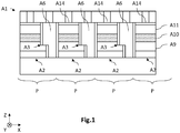
- this optoelectronic device A1 comprises a plurality of light-emitting diodes A2 each comprising a stack of a p-doped portion A11 and of an n-doped portion A9 separated from each other by an active zone A10 from which is mainly generated the light radiation from diode A2.
- the light-emitting diodes A2 have a so-called mesa structure, that is to say they are obtained from a stack of semiconductor layers intended to form the portions A9, A11 doped n and p as well as the active zone A10, a localized etching being carried out so as to individualize the light-emitting diodes A2 from one another.
- Each diode A2 has an L-shape, the sides of which are coated with an insulating layer, except at the level of a step A3 formed by the n-doped portion A9.
- First electrodes A14 rest on the upper surface of the p-doped portions A11 and second electrodes A6 extend between the diodes A2 and come into contact with the cutouts A3 formed by the n-doped portions A9.
- a display pixel then comprises the stack of doped portions A9, A11, of the active zone A10, and of the first electrode A14, as well as the second electrode A6 adjacent to the stack.
- a connection structure is assembled on the upper face of the matrix of light-emitting diodes and is intended to be hybridized to an integrated control circuit.
- This optoelectronic device however has the drawback of requiring an etching step of the doped semiconductor layers and of the active layer in order to individualize the diodes. Now, this etching step can lead to the formation of structural defects liable to degrade the optical and / or electronic properties of the diodes.
- the ratio between the emissive area of each diode on the area of each pixel is reduced by the need to form a step in the n-doped portion and by the presence of the second electrode which extends between the diodes so as to come into contact with this recess. This thus reduces the maximum light intensity relative to each pixel.
- the document WO2014 / 064276 describes a method of manufacturing an optoelectronic device comprising epitaxial wire diodes from nucleation pads which rest on a substrate and are separated from each other by a dielectric zone extending in the substrate.
- WO2014 / 056762 describes a method of manufacturing an optoelectronic device comprising the elimination of the growth substrate and the elimination of an upper part of the diodes to then allow them to be electrically polarized by means of conductive strips.
- the document US2013 / 112944 describes an optoelectronic device comprising a plurality of wire diodes arranged in distinct pixels, the wire diodes of the same pixel being covered with a conductive layer.
- the support may comprise an electrically insulating substrate, an upper face of which forms said front face, or may comprise a layer or a substrate, semiconductor or electrically conductor, coated with a so-called lower insulating layer, one face of which forms said front face.
- Each nucleation conductive strip can extend longitudinally on the front face, being electrically separated from its neighbors, transversely, by said intermediate insulating layer.
- Each upper conductive strip can extend longitudinally over the intermediate insulating layer, being electrically separated from its neighbors, transversely, by a so-called upper insulating layer.
- the upper conductive strips may be of an at least partially transparent conductive material, and may at least partially cover the second doped portions.
- Each upper conductive strip may include parts covering the second doped portions of a set of diodes, said so-called covering parts being connected to one another by so-called connecting parts resting on the intermediate insulating layer.
- the connecting parts of the upper conductive strips can be coated at least in part with a metal layer.
- the optoelectronic device may include first connection pads resting on said rear face, and electrically connected to the conductive nucleation strips by first orifices passing through the support and filled with a conductive material, and / or may include second connection pads resting on said rear face, and electrically connected to the upper conductive strips by second orifices passing through the support and the intermediate insulating layer and filled with a conductive material.
- the optoelectronic device may comprise an integrated control circuit assembled to the support and electrically connected to the nucleation conductive strips and to the upper conductive strips, adapted to apply a potential difference, sequentially, to different subsets of diodes, the diode or diodes of 'a same subset being in contact with the same nucleation conductive strip and with the same upper conductive strip, the diode (s) of different diode subsets being in contact with different nucleation conductive strips and / or of different upper conductive bands.
- At least one diode in contact with a first conductive nucleation strip and a first upper conductive strip may be connected in series with at least another diode, the latter being in contact with a second conductive nucleation strip distinct from the first nucleation strip and a second upper conductive strip distinct from the first upper strip.
- the support can be formed from a substrate made of a monocrystalline material forming an upper surface, on which rests a so-called lower insulating layer made of a dielectric material, epitaxied from the upper surface of the substrate and forming an opposite upper surface, the conductive strips nucleation being in a material comprising a transition metal forming a crystalline nucleating material, epitaxied from the upper surface of the lower insulating layer and forming a nucleation surface on which the first doped portions of said diodes are in contact.
- the material of the lower insulating layer can be chosen from aluminum nitride and oxides of aluminum, titanium, hafnium, magnesium and zirconium, and has a hexagonal, face-centered cubic or orthorhombic crystal structure.
- the material of the nucleation conductive bands can be chosen from titanium, vanadium, chromium, zirconium, niobium, molybdenum, hafnium, tantalum and tungsten, or from a nitride or a carbide of titanium or vanadium , chromium, zirconium, niobium, molybdenum, hafnium, tantalum and tungsten, and exhibits a face-centered hexagonal or cubic crystal structure. It may as a variant be a material based on gallium nitride, for example GaN, AIGaN, InGaN, or AlInGaN.
- the monocrystalline material of the substrate can be chosen from a III-V compound, a II-VI compound, or an element or compound IV, and has a face-centered hexagonal or cubic crystal structure.
- the invention also relates to a method for producing the optoelectronic device according to any one of the preceding characteristics, comprising a step of epitaxial growth of the conductive bands of nucleation by cathodic sputtering at a growth temperature between room temperature and 500 ° C. .
- an optoelectronic device with diodes for example light emitting diodes having a three-dimensional shape which each have a first doped portion and a second doped portion arranged to form a p-n junction.
- the diodes can be light emitting diodes adapted to emit light radiation or be photodiodes adapted to receive light radiation.
- the three-dimensional shape of the diodes may be such that the diodes have a wire shape, a pad shape, a pyramidal shape or the like.
- the first doped portions of the diodes extend along a longitudinal axis substantially orthogonal to the main plane of the support.
- the optoelectronic device comprises first electrodes adapted to bring the first doped portions of the diodes to a first electric potential V1, and second electrodes adapted to bring the second doped portions to a second electric potential V2.
- the first electrodes are in the form of conductive nucleation bands, distinct from one another, on which the first doped portions rest and are in contact.
- the second electrodes are in the form of so-called upper conductive strips, distinct from each other, in contact with the second doped portions.
- a three-dimensional direct coordinate system (X, Y, Z), where the X and Y axes form a plane parallel to the main plane of the substrate, and where the Z axis is oriented in a substantially orthogonal manner to the growing side of the substrate.
- the terms “vertical” and “vertically” are understood to relate to an orientation substantially parallel to the Z axis
- the terms “lower” and “upper” are understood to relate to an increasing positioning when one moves away from the growth face of the substrate in the + Z direction.
- conductive strip is meant an area of a semiconductor or conductive material, deposited in a thin layer, which has a longitudinal dimension in the plane (X, Y), or length, greater than the transverse dimension in the plane (X, Y ), or width, and the thickness dimension along the Z axis.
- Each conductive nucleation strip of index i is in contact with a set D i of several diodes which are in contact with different upper conductive strips.
- each upper conductive strip of index j is in contact with a set D j of several diodes which are in contact with different conductive nucleation strips.
- the diode (s) which are in contact with the same conductive nucleation strip of index i and of the same upper conductive strip of index j form a pixel P of indices i, j.
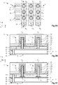
- FIGS. 2A, 2B and 2C are schematic and partial views, respectively in top view, in cross section along plane AA and along plane BB, of an optoelectronic device 1 with light-emitting diodes 2 according to a first embodiment.
- each pixel P ij comprises a single diode, but it may alternatively comprise a plurality of diodes.
- each nucleation conductive strip 6 i is in contact with a set D i of diodes, distributed into subsets P ij distinct from one another.
- Each subset P ij of diodes of the same nucleation conductive strip 6 i is in contact with the same upper conductive strip 14 of index j and form a pixel P ij .
- the support 3 has two faces, called front 3b and rear 3a, opposite to each other. It can be a one-piece structure, or be formed from a stack of layers such as a substrate 4 of the SOI type (for Silicon On Insulator, in English). It comprises an electrically insulating material at the level of the front face 3b. It can thus be formed, for example, of a one-piece insulating substrate 4, or be formed of a semiconductor or conductive substrate 4, the upper face of which is coated with an insulating layer 5.
- the material of the substrate 4 can be electrically insulating, such as for example a silicon oxide (for example SiO2) or sapphire, or be a semiconductor material for example chosen from III-V compounds comprising at least one element from column III and at least one element from column V of the periodic table, compounds II-VI or elements or compounds IV.
- a silicon oxide for example SiO2
- a semiconductor material for example chosen from III-V compounds comprising at least one element from column III and at least one element from column V of the periodic table, compounds II-VI or elements or compounds IV.
- it can be silicon, germanium, silicon carbide.
- the semiconductor material of the substrate 4 is monocrystalline silicon.
- the substrate 4 can have a thickness of between 50 nm and 1500 ⁇ m, depending on whether it has been thinned or not.
- the support has been thinned in order to allow electrical contact to be taken up on the rear face 3a
- it has a thickness for example between 10 ⁇ m and 300 ⁇ m, preferably between 10 ⁇ m and 100 ⁇ m.
- it has a thickness of between 300 ⁇ m and 1500 ⁇ m, for example equal to approximately 725 ⁇ m.
- the support is formed from a semiconductor substrate 4, the upper face of which is coated with a so-called lower insulating layer 5 made of a dielectric material.
- the lower insulating layer 5 provides electrical insulation between the conductive nucleation strips 6 i and the substrate 4 when the latter is electrically conductive.
- the material of the lower insulating layer 5 can be a silicon oxide (for example SiO2) or aluminum (for example Al2O3), a silicon nitride SiNx or aluminum AIN, a silicon oxynitride SiOxNy, or any other material. adapted.
- the thickness of the lower insulating layer 5 may be between 5 nm and 500 nm, preferably between 10 nm and 100 nm, for example equal to approximately 30 nm.
- the substrate can be omitted and the support can then be formed from a deposited layer, for example a reflective layer, possibly metallic, allowing the reflection of the incident light radiation. emitted by the diodes 2.
- the steps of removing the substrate and depositing the layer of the support can be carried out after the diodes have been produced.
- the first polarization electrodes are arranged so as to allow the application of a first electric potential V1 i to different sets of diodes. They take the form of a plurality of nucleation conductive strips 6 i which rest on the front face 3b of the support, here the upper face of the lower insulating layer 5. Each nucleation conductive strip 6 i has an upper face, opposite to the front face 3b of the support, which forms a nucleation surface on which each first doped portion 9 of diode 2 is in contact.
- the nucleation conductive bands 6 i are distinct from one another and may have an electric potential V1 i which varies over time, the value of which may be different from one band to another.
- Each conductive nucleation strip 6 of index i is in contact with a set D i of diodes at the level of the first doped portions 9 thereof, the sets of diodes being different from a conductive nucleation strip 6 i to l 'other.
- the nucleation conductive bands 6 i are made of an electrically conductive material suitable for the nucleation and the growth of the first doped portions 9.
- This material may be gallium nitride GaN, or an alloy based on gallium nitride, for example gallium and aluminum nitride AlGaN, gallium and indium nitride InGaN, or even gallium, aluminum and indium nitride AlInGaN.
- the nucleation conductive bands 6 i can alternatively be made of a material comprising a transition metal.
- It can be chosen from titanium, vanadium, chromium, zirconium, niobium, molybdenum, hafnium, tantalum and tungsten, or from a nitride or a transition metal carbide, for example of titanium, of zirconium, hafnium, vanadium, niobium, tantalum, chromium, molybdenum, tantalum, or a combination of these compounds.
- the transition metals, as well as their nitrides and carbides, have the advantages of allowing the nucleation of the first doped portions 9 and of having an electrical conductivity close to that of the metals.
- the nucleation conductive strips 6 i have a thickness for example between 5 nm and 500 nm, preferably between 10 nm and 100 nm, for example equal to approximately 30 nm. They have a transverse dimension in the plane (X, Y), or width, for example between 20 nm and 50 ⁇ m, preferably between 200 nm and 10 ⁇ m, preferably between 800 nm and 5 ⁇ m, for example equal to approximately 1 ⁇ m.
- the nucleation conductive bands 6 i are spaced transversely from one another by a distance for example between 500 nm and 20 ⁇ m, preferably between 1000 nm and 2000 nm, for example equal to 1500 nm.
- the optoelectronic device 1 further comprises a so-called intermediate insulating layer 7 which covers the front face 3b of the support, and in particular covers the conductive nucleation bands 6 i . It forms a growth mask allowing epitaxial growth of the first doped portions 9 of the diodes from through openings 8 opening locally on the nucleation surfaces. In addition, it extends so as to separate each conductive nucleation strip 6 i , transversely, from its neighbors. It also participates in ensuring the electrical insulation between the nucleation conductive bands 6 i and the upper conductive bands 14 j .
- the intermediate insulating layer 7 is made of one or more dielectric materials such as, for example, a silicon oxide (for example SiO2) or a silicon nitride (for example Si3N4 or SiN), or even a silicon oxynitride, an oxide of silicon. aluminum (eg Al2O3) or an oxide of hafnium (eg HfO2).
- the thickness of the intermediate insulating layer 7 may be between 5 nm and 500 nm, preferably between 30 nm and 300 nm, for example equal to approximately 100 nm.
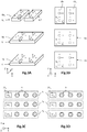
- Each light-emitting diode 2 comprises a first doped portion 9, of three-dimensional shape.
- the first doped portions 9 have an elongated shape along a longitudinal axis ⁇ , that is to say, the longitudinal dimension of which along the longitudinal axis ⁇ is greater than the transverse dimensions.
- the first doped portions 9 are then called “wires”, “nanowires” or “microwires”.
- the transverse dimensions of the wires 9, that is to say their dimensions in a plane orthogonal to the longitudinal axis ⁇ can be between 10 nm and 10 ⁇ m, for example between 100 nm and 10 ⁇ m, and preferably between 100 nm and 5 ⁇ m.
- the height of the wires 9, that is to say their longitudinal dimension along the longitudinal axis ⁇ , is greater than the transverse dimensions, for example 2 times, 5 times and preferably at least 10 times greater.
- the cross section of the wires 9, in a plane orthogonal to the longitudinal axis ⁇ , can have different shapes, for example a circular, oval, polygonal, for example triangular, square, rectangular or even hexagonal shape.
- the diameter is defined here as being a quantity associated with the perimeter of the wire at the level of a straight section. It may be the diameter of a disc having the same area as the cross section of the wire.
- the local diameter is the diameter of the wire at a given height thereof along the longitudinal axis ⁇ .
- the mean diameter is the average, eg arithmetic, of local diameters along the wire or a portion thereof.
- Each first doped portion 9 extends from the nucleation surface of a conductive nucleation strip 6 i , along a longitudinal axis ⁇ oriented substantially orthogonal to the plane (X, Y).
- Each diode 2 further comprises an active zone and a second doped portion 11.
- the wire 9 here forms the heart of a light emitting diode. 2 in the core / shell configuration, the active zone and the second doped portion 11 covering the lateral border of a so-called upper part 13 of the wire 9.
- the wires 9 comprise a lower part 12 which is in contact with the nucleation surfaces and is surrounded by by the intermediate insulating layer 7. This lower part 12 is extended by the upper part 13 which is located outside the growth openings 8 and is covered by the active zone and the second doped portion 11.
- the wires 9 can be made of a crystalline material epitaxied from the nucleation surface.
- the material of the wires 9 predominantly comprises a first semiconductor compound which can be chosen from III-V compounds and in particular from III-N compounds, from II-VI compounds or from compounds or elements IV.
- III-V compounds can be compounds such as GaN, InGaN, AIGaN, AIN, InN or AlInGaN, or even compounds such as AsGa or InP.
- II-VI compounds can be CdTe, HgTe, CdHgTe, ZnO, ZnMgO, CdZnO, CdZnMgO.
- Elements or compounds IV can be Si, C, Ge, SiC, SiGe, GeC.
- the wires 9 thus form the first portions of the diodes, and are doped according to a first type of conductivity, here of type n.
- the wires 9 are made of n-type doped GaN, in particular with silicon. They have here an average diameter of between 10 nm and 10 ⁇ m, for example between 500 nm and 5 ⁇ m and is here substantially equal to 500 nm.
- the height of the wires 9 can be between 100 nm and 100 ⁇ m, for example between 500 nm and 50 ⁇ m, and is here substantially equal to 5 ⁇ m.
- the active area is the portion of diode 2 at which the main part of the light radiation from the diode is emitted. It can comprise at least one quantum well made of a semiconductor compound having a band gap energy lower than those of the wire 9 and of the second doped portion 11. It covers here the upper edge and the side edge of the wire 9. It can include a single quantum well or a plurality of quantum wells in the form of layers or boxes interposed between barrier layers. Alternatively, the active area may not include a quantum well. It can have a band gap energy substantially equal to that of the wire 9 and of the second doped portion 11. It can be made from a semiconductor compound that is not intentionally doped.
- the second doped portion 11 forms a layer which covers and at least partially surrounds the active zone. It is produced from a second semiconductor compound doped according to a second type of conductivity opposite to the first type, that is to say here of p type.
- the second semiconductor compound may be the same as the first semiconductor compound of the yarn or may include the first semiconductor compound and further one or more additional elements.
- the second doped portion 11 may be GaN or InGaN, p-type doped in particular with magnesium.
- the thickness of the second doped portion 11 may be between 20nm and 500nm, and may be equal to approximately 150nm.
- the types of conductivity of the first and second portions 9, 11 can be reversed.
- the second doped portion 11 may further comprise an intermediate electron blocking layer (not shown) located at the interface with the active zone.
- the electron blocking layer can here be formed from a ternary III-N compound, for example AlGaN or AlInN, advantageously p-doped. It makes it possible to increase the rate of radiative recombinations in the active zone.
- the second polarization electrodes 14 j are arranged so as to allow the application of a second electric potential V2 j to different sets of diodes. They take the form of a plurality of so-called upper conductive strips 14 j which rest on the upper face of the intermediate insulating layer 7. They are distinct from each other and may have an electrical potential V2 j which varies over time, including the value may be different from one band to another. They are also electrically separated from the nucleation conductive strips 6i by the intermediate insulating layer 7. They can extend longitudinally in the plane (X, Y) in a rectilinear or curved manner, parallel to each other.
- each upper conductive strip 14 j extends longitudinally and comprises parts 15 j covering the second doped portions 11 of said diodes 2 which are interconnected by so-called connecting parts 16 j extending substantially. flat on the upper face of the intermediate insulating layer 7.
- Each upper conductive strip 14 of index j is in contact with a set D j of diodes 2 at the level of the second doped portions 11 thereof, the sets D j of diodes 2 being different from an upper conductive strip 14 j to the other.
- the upper conductive bands 14 j extend transversely to the nucleation conductive bands 6 i , so that a set D i of diodes 2 in contact with a nucleation conductive band 6 of index i is not identical to a set D j of diodes 2 in contact with an upper conductive strip 14 j .
- the intersection between a set D i of diodes 2 of a nucleation conductive strip 6 of index i with a set D j of diodes 2 of an upper conductive strip 14 of index j forms a pixel P ij .
- the upper conductive strips 14 j are made of an electrically conductive material, and, when they cover the second doped portions 11, advantageously transparent to the light radiation emitted by the diodes. It can be, for example, an indium tin oxide (ITO, for Indium Tin Oxide in English) or a zinc oxide doped with gallium (GZO, for Gallium doped Zinc Oxide in English), even doped with aluminum or indium.
- ITO indium tin oxide
- GZO gallium doped Zinc Oxide in English
- transparent, or at least partially transparent is meant a material which transmits at least 50% of the incident light, and preferably at least 80% or even more.
- the upper conductive strips 14 j have a thickness for example between 5 nm and 500 nm, preferably between 10 nm and 100 nm, for example equal to approximately 50 nm. They have a transverse dimension in the plane (X, Y), or width, for example between 20 nm and 50 ⁇ m, preferably between 200 nm and 10 ⁇ m, preferably between 800 nm and 5 ⁇ m, for example equal to approximately 1.5 ⁇ m. The width is such that each upper conductive strip 14 j is electrically separated from its neighbors.
- the length of the upper conductive strips 14 j is such that each upper conductive strip 14 j is in contact with the second doped portions 11 of a set of diodes 2 which are in contact with different nucleation conductive strips 6 i .
- the upper conductive strips 14 j are spaced transversely from one another by a distance for example between 1000 nm and 10 ⁇ m, preferably between 1000 nm and 3000 nm, for example equal to 2500 nm.
- It can be made of a dielectric material transparent to light radiation. emitted by the diodes, for example, an oxide of silicon (for example SiO2) or aluminum (for example Al2O3), a silicon nitride SiNx or aluminum AIN, a silicon oxynitride SiOxNy, or any other suitable material. It has a thickness for example between 5 nm and 500 nm, preferably between 50 nm and 300 nm, for example equal to approximately 100 nm.
- a reflective layer 19 is present between the diodes 2 and rests on the upper insulating layer 18 without however covering the wires 9. It is made of a material suitable for reflecting the incident light radiation emitted by the diodes 2 in the direction of outside the optoelectronic device 1, in the + Z direction.
- the material can be a metal, for example aluminum, silver, gold, copper, or a combination thereof, or any other suitable material.
- the reflective layer 19 has a thickness for example between 10 nm and 2 ⁇ m, preferably between 100 nm and 500 nm, for example equal to approximately 200 nm.
- an encapsulation layer 20 covers the diodes. It is made of a dielectric material at least partially transparent to the light radiation emitted by the diodes, and can be, for example, a silicon oxide (for example SiO2) or aluminum (for example Al2O3), a silicon nitride SiNx or aluminum AIN, a silicon oxynitride SiOxNy, or any other suitable material.
- the thickness of the encapsulation layer 20 is such that it covers the diodes, in particular at their top. It is included, for example, between 500nm and 50 ⁇ m.
- the optoelectronic device 1 also comprises a plurality of first connection pads 21 i each being electrically connected to a conductive nucleation strip 6 i .
- the first connection pads 21 i can be located on the front face 3b or on the rear face 3a of the support. In this example, the electrical connection is made on the rear face 3a of the support.
- first through orifices 22 i extend between the front 3b and rear 3a faces of the support and each open out onto a conductive nucleation strip 6 i .
- the through orifices 22 i are filled with a conductive material 23 and are in contact, on the one hand with the material of the conductive nucleation strip 6 i and on the other hand with a first connection pad 21 i .
- the flanks of the through holes 22 i are coated with an insulating layer 24.
- the filling material 23 and that of the first connection pads 21 i can be copper, gold, aluminum or any other suitable conductive material.
- the optoelectronic device 1 also comprises a plurality of second connection pads 25 j each being electrically connected to an upper conductive strip 14 j .
- the second connection pads 25 j can be located on the front face 3b or on the rear face 3a of the support. In this example, the electrical connection is made on the rear face 3a of the support.
- second through orifices 26 j extend between the front 3b and rear 3a faces of the support and each open out onto an upper conductive strip 14 j .
- the through orifices 26 j are filled with a conductive material 23 and are in contact, on the one hand with the material of the upper conductive strip 14 j and on the other hand with a second connection pad 25 j .
- the flanks of the through holes 26 j are coated with an insulating layer 24.
- the filling material 23 and that of the second connection pads 25 j can be made of copper, gold, aluminum or any other suitable conductive material.
- An insulating layer 27 may cover the rear face 3a of the support so as to electrically insulate the first and second connection pads 21 i and 25 j from the material of the substrate 4.
- the optoelectronic device 1 comprises an integrated control circuit (not shown) assembled to the support, and electrically connected to the conductive strips of nucleation 6 i via the first connection pads 21 i , and to the upper conductive strips 14 j via the second connection pads 25 j .
- the integrated control circuit may include electronic components, for example transistors, so as to control the application of an electric potential difference, simultaneously or sequentially, to the various pixels P ij of diodes.
- the hybridization of the control circuit to the support can be carried out by direct bonding (or bonding by molecular adhesion, direct bonding ) of the metal-metal and dielectric-dielectric type. It may as a variant be carried out by intermediate connection elements made of a fusible conductive material, such as indium balls, coming into contact with the various first and second connection pads of the optoelectronic device 1.
- the control circuit can be connected to the first and second connection pads 21 i and 25 j by means of soldered electrical wires ( wire bonding, in English), in particular when the connection pads are located on the front face 3b of the support.
- the optoelectronic device 1 comprises a plurality of diodes 2 distributed in a matrix of pixels which can be activated independently of each other by means of the first and second polarization electrodes which are in the form of conductive strips distinct from each other.
- the fact that the first polarization electrodes have an additional function of nucleation surface makes it possible to simplify the structure as well as the production process.
- Each pixel may further include a developed area of the active area substantially equal to or greater than the area, in the (X, Y) plane, of the pixel, so that the maximum light emission intensity of the optoelectronic device 1 can be greater than that of the optoelectronic device 1 of the prior art mentioned above. A high light intensity and high resolution optoelectronic device 1 is thus obtained.
- the optical and / or electronic properties of the diodes 2 exhibit improved homogeneity from one diode to another.
- the substrate 4 has an upper surface 4b formed by a monocrystalline material;
- the lower insulating layer 5 is made of a crystalline material epitaxied from the upper surface 4b of the substrate 4; and
- the nucleation conductive bands 6i are made of a material comprising a transition metal epitaxied from the crystalline material of the lower insulating layer 5.
- the substrate 4 comprises a monocrystalline growth material at least at the level of the upper surface 4b.
- the growth material is formed from a single crystal and therefore does not include several crystals separated from each other by grain boundaries.
- the material of the substrate 4 has crystallographic properties, in terms of lattice parameter and type of structure, suitable for the epitaxial growth of a crystalline material of the lower insulating layer 5.
- it preferably has a crystalline structure of the type. face-centered cubic oriented in the [111] direction or a hexagonal crystal structure oriented in the [0001] direction.
- the material of the substrate 4 is monocrystalline silicon, with a face-centered cubic-type crystal structure, the growth plane of which is oriented in the [111] direction, and the lattice parameter a s of which is approximately 3.84 ⁇ .
- the lower insulating layer 5 is made of a crystalline material epitaxied from the upper surface 4b of the substrate 4.
- the material of the lower insulating layer 5 comprises a crystal lattice in epitaxial relation with that of the monocrystalline material of the substrate.
- the crystal lattice of the material of the lower insulating layer 5 has an elementary cell defined in particular by its crystallographic axes denoted here, purely by way of illustration, a i , b i , c i .
- the crystal lattice therefore has an alignment of at least one crystallographic axis a i , b i oriented in the plane of the material and of at least one crystallographic axis c i oriented orthogonally to the plane of the material, with the crystallographic axes a s , b s and c s of the single crystal material of the substrate, respectively.
- This results in the fact that the crystallographic axis a i is substantially parallel, at any point of the upper surface 5b, to the crystallographic axis a s , just like, respectively, the crystallographic axes b i and c i relative to the axes crystallographic b s and c s .
- each crystallographic axis a i , b i , c i is substantially identical at all points of the upper surface 5b.
- the crystallographic axes a i are substantially identical, that is to say mutually parallel, at any point of the upper surface 5b, just like, respectively, the crystallographic axes b i and c i .
- a polycrystalline material is formed, unlike a monocrystalline material, of several crystals separated from each other by grain boundaries.
- the material of the lower insulating layer 5 exhibits crystallographic properties, in terms of lattice parameter and type of crystal structure, such that it is suitable for being epitaxied from the single crystal material of the substrate 4. It is furthermore suitable for allow the epitaxial growth of the nucleation conductive bands 6 i of a material comprising a transition metal from the upper surface 5b. It preferably has a lattice parameter such that the lattice mismatch with the monocrystalline material of the substrate 4 is less than or equal to 20%.
- the type of the crystal structure is such that its crystallographic axes a i , b i , c i can be respectively parallel to the axes a s , b s , c s of the single crystal material of the substrate.
- the crystal structure may be of the face-centered cubic type, oriented in the [111] direction, or of the hexagonal type oriented in the [0001] direction, or even of the orthorhombic type oriented in the [111] direction.
- the material of the lower insulating layer 5 is aluminum nitride AlN, with a mesh parameter of approximately 3.11 ⁇ , and with a crystalline structure of the hexagonal type, the growth plane of which is oriented in the [0001] direction.
- the nucleation conductive bands 6 i are made of a material comprising a transition metal epitaxied from the upper surface 5b of the lower insulating layer 5.
- the nucleation material comprises a crystal lattice epitaxially related to that of the material of the nucleation. lower insulating layer 5.
- the crystal lattice of the nucleating material has an elementary cell defined in particular by its crystallographic axes denoted here, purely by way of illustration, a n , b n , c n .
- the crystal lattice therefore has an alignment of at least one crystallographic axis a n , b n oriented in the plane of the material and at least one crystallographic axis c n oriented orthogonally to the plane of the material, with the crystallographic axes a i , b i , and c i , of the material of the lower insulating layer 5, respectively, at the level of the upper surface 5b.
- each crystallographic axis a n is identical at all points of the nucleation surface 6b.
- the crystallographic axes a n are identical, that is to say mutually parallel, at all points of the nucleation surface 6b, just like, respectively, the crystallographic axes b n and c n .
- the nucleation material exhibits crystallographic properties, in terms of lattice parameter and type of structure, such that it can be epitaxied from the material of the lower insulating layer 5. It is furthermore suitable for epitaxial growth, at from the nucleation surface 6b, of a wire 9. Preferably, it thus has a mesh parameter such that the mesh mismatch with the material of the lower insulating layer 5 is less than or equal to 20%.
- the type of the crystal structure is such that its crystallographic axes a n , b n , c n can be respectively parallel to the axes a i , b i , c i of the material of the lower insulating layer 5.
- the crystal structure can be respectively be of the face-centered cubic type, oriented in the direction [111] or of the hexagonal type oriented in the direction [0001], or even of the orthorhombic type oriented in the direction [111].
- the nucleation material comprises a transition metal, i.e. it can be a transition metal or a compound comprising a transition metal, for example a nitride or a carbide of a transition metal . Transition metals, as well as their nitrides and carbides, have in particular the advantage of good electrical conductivity, close to that of metals.
- the nucleation material can be chosen from titanium Ti, zirconium Zr, hafnium Hf, vanadium V, niobium Nb, tantalum Ta, chromium Cr, molybdenum Mo and tungsten W, a nitride of these elements TiN , ZrN, HfN, VN, NbN, TaN, CrN, MoN, or WN, or a carbide of these elements TiC, ZrC, HfC, VC, NbC, TaC, CrC, MoC, WC.
- the transition metal nitrides and carbides may contain an atomic proportion of transition metal other than 50%.
- the nucleation material is chosen from a nitride of titanium TiN, zirconium ZrN, hafnium HfN, vanadium VN, niobium NbN, tantalum TaN, chromium CrN, molybdenum MoN or tungsten WN, or a titanium TiN, zirconium ZrN, hafnium HfN, vanadium VN, niobium NbN, or tantalum TaN carbide.
- the nucleation material is chosen from a nitride or a carbide of titanium TiN, TiC, of zirconium ZrN, ZrC, of hafnium HfN, HfC, of vanadium VN, VC, of niobium NbN, NbC, or of tantalum TaN, TaC.
- the nucleation material is chosen from a nitride of titanium TiN, zirconium ZrN, hafnium HfN, niobium NbN, or tantalum TaN.
- the nucleation material is chosen from a hafnium HfN or niobium NbN nitride.
- the first doped portions 9 of the diodes 2 are epitaxied from the nucleation surfaces 6b of the various nucleation conductive bands 6 i .
- the wire material has a crystal lattice epitaxially related to that of the nucleation material.
- the crystal lattice of the wire material has an elementary mesh defined in particular by its crystallographic axes denoted here, purely by way of illustration, a f , b f , c f .
- the crystallographic axes a f , b f , c f of the wire material are respectively substantially parallel to the crystallographic axes a n , b n , c n of the nucleation material at the level of the nucleation surface 6b.
- the crystallographic axis a f is parallel to the crystallographic axis a n of the nucleation surface 6b. It is the same for the crystallographic axes b f and c f relative to the crystallographic axes b n and c n .
- each crystallographic axis a f , b f , c f is identical from one wire 9 to another.
- the crystallographic axes a f are identical, that is to say parallel to each other, from one wire to the other. It is the same for the crystallographic axes b n and c n .
- the wires exhibit substantially identical crystallographic properties, in terms of orientation and position of the crystal lattice.
- the optoelectronic device 1 thus exhibits substantially homogeneous crystallographic properties at the level of the wires, which helps to homogenize the electrical and / or optical properties of the light-emitting diodes 2.
- the transition metal nitride nucleation portions are epitaxial and not only textured when they are deposited on an epitaxial lower insulating layer, and not directly from it. the upper surface 4b of the single crystal material of the substrate.
- the epitaxial crystalline material comprises a crystal lattice, or crystal structure, in epitaxial relation with that of the nucleation material from which it is epitaxied.
- epitaxy relationship is meant that the epitaxial material exhibits an alignment of the crystallographic orientations of its crystal lattice, in at least one direction in the plane of the material and at least one direction orthogonal to the plane of the material, with those of the crystal lattice of the material. nucleation material.
- the plane of the epitaxial material is here a plane of growth of the material, parallel to the nucleation surface. The alignment is preferably carried out within 30 °, or even within 10 °.
- a crystalline material is epitaxied from a nucleating crystalline material, i.e.
- the epitaxial relationship between these two crystalline materials results in the fact that at least a crystallographic axis of the crystal lattice of the epitaxial material, oriented in the plane of the epitaxial material, for example a e and / or b e , and at least one crystallographic axis, oriented orthogonally to the plane, for example c e , are respectively substantially parallel to the crystallographic axes a n and / or b n , and c n of the crystal lattice of the nucleation material.
- An epitaxial material is a particular case of so-called textured materials in the sense that the textured materials have a preferential crystallographic direction oriented orthogonally to the plane of the material, but do not have a preferential crystallographic direction oriented in the plane of the material. Furthermore, the preferential crystallographic direction orthogonal to the plane of the textured material is not, or only slightly, dependent on the crystalline properties of the nucleation material. Thus, a textured material has a single preferred crystallographic direction, for example that of the c axis and not three preferred directions. The lattice of the textured material then has a polycrystalline structure in which the different crystalline domains, separated by grain boundaries, are all oriented along the same privileged crystallographic axis c.
- the c axes of the crystalline domains are mutually parallel but the a axes, like the b axes, are not mutually parallel and are oriented in a substantially random manner.
- This preferred crystallographic direction is not, or is not very dependent on the crystalline properties of the nucleation material.
- the wires 9, here in GaN epitaxied by MOCVD when they are epitaxied from a textured nucleation material and not epitaxied, all have the same direction of growth, the latter being substantially parallel to the crystallographic axis c n .
- the hexagonal shape of the wires 9 is not oriented identically from one wire to another, which reflects the fact that the crystallographic axes a f and b f are not respectively oriented in such a way. identical from one wire to another.
- the wires 9 then have crystallographic properties that are different from one wire to another, which can result in a certain inhomogeneity in the electrical and / or optical properties of the light-emitting diodes 2.
- the wires 9, here in GaN epitaxied by MOCVD when they are epitaxied from an epitaxial nucleation material and not textured, all have the same direction of growth, the latter being substantially parallel to the crystallographic axis c n .
- the hexagonal shape of the wires 9 is here oriented identically for all the wires 9, which reflects the fact that the crystallographic axes a f and b f are respectively oriented identically from one wire to the other. 'other.
- the wires 9 have crystallographic properties, in terms of orientation and position of the crystal lattice, which are substantially identical.
- the device optoelectronics 1 thus exhibits substantially homogeneous crystallographic properties at the level of the wires 9, which helps to homogenize the electrical and / or optical properties of the light-emitting diodes 2.
- FIGS. 4A to 4I schematically and partially illustrate, in cross section, various steps of an exemplary method of making the optoelectronic device 1 according to the preferred embodiment described above.
- Each figure illustrates a sectional view along the plane AA (left) and a sectional view along the plane BB (right).
- the substrate 4 is provided, the material of which is monocrystalline at least at the level of the upper surface.
- the substrate 4 is made of silicon, the structure of which is of the face-centered cubic type oriented in the direction [111]. Its mesh parameter in the plane of the upper surface is of the order of 3.84 ⁇ .
- the lower insulating layer 5 is deposited, so as to cover the upper surface of the substrate, by a method of the chemical vapor deposition (CVD) type, for example with organometallic precursors (MOCVD, for Metal-Organic Chemical Vapor Déposition, in English) or by a method of the epitaxy type by molecular beams (MBE, for Molecular-Beam Epitaxy, in English), of the hydride vapor phase epitaxy (HVPE, for Hybrid Vapor Phase Epitaxy) , in English), of the type epitaxy by atomic layer (ALE, for Atomic Layer Epitaxy, in English) or deposition by atomic layer (ALD, for Atomic Layer Deposition, in English), even by evaporation or by cathodic sputtering (sputtering, in English) English).
- CVD chemical vapor deposition
- MOCVD Metal-Organic Chemical Vapor Déposition
- MBE molecular beams
- HVPE hydride vapor phase
- the material of the lower insulating layer 5 is epitaxial aluminum nitride, the crystal structure of which is of the hexagonal type and is oriented in the [0001] direction. Its mesh parameter in the (X, Y) plane is of the order of 3.11 ⁇ . It is filed by MOCVD.
- the nominal V / III ratio defined as the ratio between the molar flux of elements from column V on the molar flux of elements from column III, i.e. here the N / Al ratio, is included between 200 and 1000.
- the pressure is of the order of 75 torr.
- the growth temperature T measured at the level of the substrate, may firstly be greater than or equal to 750 ° C. for the nucleation phase, then secondly of the order of 950 ° C. for the growth phase.
- the nucleation conductive bands 6i are formed on the upper surface of the lower insulating layer 5.
- the growth is carried out epitaxial of a layer of a nucleation material in a material comprising a transition metal, for example by a cathode sputtering technique, the growth temperature of which is advantageously between room temperature, for example 20 ° C, and 1000 ° C.
- the nucleation bands are also epitaxial when they are deposited by sputtering with a growth temperature between room temperature, for example 20 ° C, and 500 ° C, for example a temperature substantially equal to 400 ° vs.
- the power can be of the order of 400W.
- the pressure can be of the order of 8.10 -3 torr.
- High temperature sputtering and chemical vapor deposition techniques can also be used.
- the etching of the continuous layer of nucleation material is then carried out by conventional photolithography and etching techniques to form a plurality of nucleation conductive bands 6i distinct from each other.
- a crystallization annealing step can be carried out so as to obtain a monocrystalline nucleation material.
- the annealing can be carried out at an annealing temperature corresponding substantially to the crystallization temperature of the nucleation material, namely 1620 ° C. in the case here of the transition metal nitride.
- the crystallization of the nucleating material can also be obtained at an annealing temperature lower than the crystallization temperature, for example in a temperature range from 600 ° C to 1620 ° C, preferably between 800 ° C and 1200 ° C, for example equal to approximately 1000 ° C.
- the annealing can be carried out for a duration for example greater than 1 min, preferably greater than 5 min, or even 10 min, for example 20 min. It can be carried out under a flow of nitrogen (N2) and ammonia (NH3).
- the pressure can be of the order of 75 torr.
- the intermediate insulating layer 7 forming a growth mask is then deposited and the through openings 8 are produced.
- a layer of a dielectric material is thus deposited so as to cover the nucleation conductive bands 6i and the lower insulating layer 5, then through openings 8 are formed so as to open locally on the nucleation surfaces.
- the dielectric material is, for example, a silicon oxide (for example SiO2) or a silicon nitride (for example Si3N4), or even a stack of several different dielectric materials. It is selectively etched with respect to the material of the nucleation conductive bands 6i.
- the lateral dimensions of the openings are smaller than the width of the conductive nucleation bands 6i, for example at least two times smaller.
- the wires 9 are formed, here in GaN, by epitaxial growth from the nucleation surfaces of the various nucleation conductive bands 6 i , through the openings of the intermediate insulating layer 7, for example according to a process identical or similar to that described in the document WO2012 / 136665 .
- the growth temperature is brought to a first value T 1 , for example between 950 ° C and 1100 ° C, and in particular between 990 ° C and 1060 ° C.
- the nominal V / III ratio here the N / Ga ratio, has a first value (V / III) 1 of between 10 and 100 approximately, for example approximately equal to 30.
- the elements of group III and of group V come from precursors injected into the epitaxy reactor, for example trimethylgallium (TMGa) or triethylgallium (TEGa) for gallium, and ammonia (NH 3 ) for nitrogen.
- TMGa trimethylgallium
- TMGa triethylgallium
- NH 3 ammonia
- the H 2 / N 2 ratio has a first value (H 2 / N 2 ) 1 greater than or equal to 60/40, preferably greater than or equal to 70/30, or even more, for example substantially equal to 90/10.
- the pressure can be set at around 100mbar.
- first doped portions 9 are obtained in the form of wires which extend along the longitudinal axis ⁇ from the nucleation surfaces.
- the first semiconductor compound of the first doped portions 9, namely here GaN, is n-type doped with silicon.
- the lower part 12 of the wires 9 is located in the openings of the intermediate insulating layer 7, and extends along the longitudinal axis ⁇ by the upper part 13.
- the upper part 13 of the wires 9 is located in the openings of the intermediate insulating layer 7, and extends along the longitudinal axis ⁇ by the upper part 13.
- the active zones are formed by epitaxial growth from the exposed surface of the wires 9, that is to say here on the upper part 13 of the wires 9. More precisely, a stack of barrier layers and at least a layer forming a quantum well, said layers being alternated in the direction of epitaxial growth.
- the layers forming the quantum wells and the barrier layers can be made of InGaN, with different atomic proportions for the quantum well layers and the barrier layers.
- the barrier layers are made of In x Ga (1-x) N with x equal to approximately 18 atomic%
- the quantum well layers are also made of In y Ga (1-y) N, with y greater than x, for example of the order of 25 atomic%, so as to improve the quantum confinement of the charge carriers in the quantum wells.
- the formation of the barrier layers and of the quantum well layers can be carried out at a growth temperature value T 3 substantially equal to the value T 2 , namely here 750 ° C.
- the V / III ratio has a value (V / III) 3 substantially equal to the value (V / III) 2 .
- the H 2 / N 2 ratio has a value substantially equal to the value (H 2 / N 2 ) 2 during the formation of the barrier layers and has a value substantially less than the value (H 2 / N 2 ) 2 during the formation of quantum well layers, for example 1/99.
- the pressure can remain unchanged. In this way, barrier layers of InGaN with approximately 18 atomic% indium are obtained and quantum well layers of InGaN with approximately 25 atomic% indium.
- the second p-doped portions are then formed by epitaxial growth so as to cover and at least partially surround the active areas.
- the growth temperature can be brought to a fourth value T 4 greater than the value T 3 , for example of the order of 885 ° C.
- the V / III ratio can be brought to a fourth value (V / III) 4 greater than the value (V / III) 3 , for example of the order of 4000.
- the H 2 / N 2 ratio is increased to a fourth value (H 2 / N 2 ) 4 greater than the value (H 2 / N 2 ) 2 , for example of the order of 15/85.
- the pressure can be reduced to a value of the order of 300mbar.
- p-doped second portions 11 are obtained, for example made of GaN or p-type doped InGaN, which here continuously cover and surround the active areas.
- the second p-doped portions 11 and the active areas thus form the shells of the diodes 2 in the core / shell configuration.
- the active zone and the second doped portion 11 of the diodes 2 cover the upper part 13 of each wire, from the upper surface of the intermediate insulating layer 7.
- the upper conductive strips 14 j distinct from each other, which extend over the upper surface of the intermediate insulating layer 7 and come into contact with the second doped portions 11 of diodes.
- a continuous layer of a conductive material and here partially transparent to the light radiation emitted by the diodes is deposited in a conformal manner.
- the upper conductive strips 14 j which are distinct from each other, are formed. They comprise here each of the parts which cover the second doped portions 11 of a set D j of diodes, these covering parts 15 j being connected in pairs by connecting parts 16 j which extend over the upper surface of the layer. intermediate insulation 7.
- the connecting parts 16 j of the upper conductive strips 14 j are covered by a metal layer 17 adapted to reduce the electrical resistance of the upper conductive strips 14 j and thus improve the flow of electric current.
- This metal layer 17 is deposited on the upper conductive strips 14 j and then is etched so as to cover only the connecting parts 16 j and not the covering parts 15 j .
- This metal layer 17 can be made of one or more materials chosen from aluminum, silver, gold or any other suitable material, and has a thickness for example between 5nm and 200nm, preferably between 10nm and 100nm, for example equal to approximately 30nm.
- the layer metal 17 can be deposited prior to the deposition of the upper conductive strips 14 j . It is etched so as not to extend around the second doped portions 11 along the Z axis.
- the upper insulating layer 18 is deposited so as to continuously cover the upper conductive strips 14 j , the metal layer 17 and the intermediate insulating layer 7.
- the upper insulating layer 18 is made of a dielectric material such as, for example, , a silicon oxide (for example SiO2) or a silicon nitride (for example Si3N4), or even a stack of several different dielectric materials.
- a reflective layer 19 is then deposited so as to cover the surface of the upper insulating layer 18 without covering the wires 9.
- the reflective layer 19 thus extends essentially in the plane (X, Y).
- This reflective layer 19 can be made of one or more materials chosen from aluminum, silver, gold or any other suitable material, and has a thickness for example between 20nm and 1500nm, preferably between 400nm and 800nm. The thickness of the reflective layer 19 is chosen so that the incident light radiation emitted by the diodes 2 is reflected in the + Z direction.
- an encapsulation layer 20 is deposited so as to completely cover the diodes.
- the encapsulation layer 20 is made of a dielectric material transparent to the light radiation emitted by the diodes 2, such as, for example, a silicon oxide (for example SiO2) or a silicon nitride (for example Si3N4), or even a stacking of several different dielectric materials.
- the thickness of the encapsulation layer 20 is for example between 250 nm and 50 ⁇ m.
- the first connection pads 21 i and the second connection pads 25 j are then carried out .
- the substrate 4 is thinnered, then the first through orifices 22 i are produced, opening out at the level of the conductive nucleation bands 6 i as well as the second through orifices 26 j emerging at the level of the upper conductive strips 14 j .
- the sides of the through-holes can be coated with an insulating layer 24, then a conductive material 23 fills the interior of the through-holes.
- the first and second connection pads 21 i and 25 j are then formed, respectively, at each first and second orifice passing through 22 i and 26 j .
- Hybridization of the support to an integrated control circuit is then carried out by molecular bonding, by wiring by wire, or by connection by means of conductive elements and fuses.
- the method for producing the optoelectronic device 1 has the advantage of not having to carry out an electrical individualization of the diodes 2 by means of insulating trenches formed between the diodes 2 from the front face 3b of the support.
- the diodes 2 are here individualized by the first and second electrodes which are in the form of conductive strips distinct from each other.
- the support has improved mechanical strength, which in particular facilitates hybridization to the control circuit.
- the diodes 2 have optical and / or electronic properties preserved insofar as the individualization of the diodes 2 does not require, as in the example of the prior art mentioned above, an etching of the doped portions and of the active area.
- the homogeneity of the optical and / or electronic properties of the diodes 2 is further improved when the diodes 2 are formed from conductive bands of nucleation 6i in epitaxial relation with the monocrystalline material of the substrate.
- each pixel P ij can include several diodes.
- the application of a potential difference to the pixel P ij leads to an activation of the diodes 2 of this pixel, the diodes 2 of the other pixels remaining deactivated.
- the optoelectronic device 1 may include an integrated routing circuit 28 comprising electrical interconnections 29 ensuring a series connection of several pixels between them.
- the diodes 2 of the pixel P 1 are connected in series with the diodes 2 of the pixel P 2 by means of the electrical interconnections 29 of the routing circuit 28 connected to the first and second through orifices 22 i , 26 j .
- the integrated routing circuit 28 can be assembled and electrically connected to the control circuit (not shown) by means of the connection pads 21 i , 25 j .
- a potential difference can be applied to the pixels P1 and P2 connected in series, by means of the connection pads 21 2 and 25 1 .
- connection pad 25 1 is applied to the upper conductive strip 14 1 of the pixel P 1 via the through-hole 26 1 and the interconnection 29.1
- the electrical potential of the connection pad 21 2 is applied to the nucleation conductive strip 6 2 of the pixel P 2 via the through orifice 22 2 and the interconnection 29.3.
- the pixels P 1 and P 2 are connected in series by the electrical connection of the nucleation conductive strip 6 1 of the pixel P 1 with the upper conductive strip 14 2 of the pixel P 2 made by the through holes 22 1 and 26 2 and l 'interconnection 29.2.
- the interconnection 29.2 can be omitted and the through holes 22 1 and 26 2 can be in electrical contact directly in the substrate 4.
- the optoelectronic device 1 can comprise one or more electrical interconnections 30 located at the level of the intermediate insulating layer 7, allowing, in this example, the placing in series of the diodes 2 of the pixel P 1 with the diodes 2 of the pixel P 2 .
- the electrical interconnection 30 is formed here of a through orifice filled with a conductive material opening on the one hand on the nucleation conductive strip 6 1 of the pixel P 1 and on the other hand on the upper conductive strip 14 2 of the pixel P 2 .
- a routing circuit 28 is provided and ensures the electrical polarization of the pixels P 1 and P 2 connected in series, by means of the interconnections 29.1 and 29.3.
- Examples of figures 6A and 6B are given purely by way of illustration and other electrical interconnection configurations internal or formed in an integrated routing circuit are possible so as to ensure a connection of the pixels in series or in parallel. Furthermore, as a variant and as mentioned above, the electrical connection pads can be located on the front face or on the rear face of the support.
- an optoelectronic device 1 with light-emitting diodes 2 which can advantageously form a display screen or an image projector with high light intensity and high spatial resolution.
- the invention also applies to the field of photodiodes adapted to receive and detect light radiation and to convert it into electrical signals relating to the various pixels.
- Three-dimensional diodes 2 of the wire type have been described, but the invention also applies to the first doped portions in the form of three-dimensional pads whose height along the Z axis is of the same order of magnitude as its transverse dimensions in the plane ( X, Y), as well as to the first doped portions in the form of possibly truncated pyramids.
- Diodes 2 in core / shell configuration have been described where the active areas and the second doped portions cover the sides and the top of the wires 9.
- the invention also applies to the axial configuration of the diodes 2 where the active areas and the second doped portions cover only the top of the wires.
- nucleation conductive bands vis-à-vis the upper conductive bands
- other orientations are possible, where the nucleation bands and the upper bands form for example two by two an angle non-zero less than or greater than 90 °.
Description
Le domaine de l'invention est celui des dispositifs optoélectroniques à diodes électroluminescentes ou à photodiodes. L'invention s'applique au domaine des dispositifs à matrice de diodes électroluminescentes tels que les dispositifs d'éclairage, les écrans d'affichage et les projecteurs d'images, ainsi qu'au domaine des dispositifs à matrice de photodiodes tels que les photodétecteurs et les capteurs.The field of the invention is that of optoelectronic devices with light-emitting diodes or photodiodes. The invention applies to the field of light-emitting diode array devices such as lighting devices, display screens and image projectors, as well as to the field of photodiode array devices such as photodetectors. and sensors.
Il existe des dispositifs optoélectroniques à matrice de diodes électroluminescentes adaptées à former des dispositifs d'éclairage, des écrans d'affichage et des projecteurs d'images. Le document
Les diodes électroluminescentes A2 présentent une structure dite mesa, c'est-à-dire qu'elles sont obtenues à partir d'un empilement de couches semiconductrices destinées à former les portions A9, A11 dopées n et p ainsi que la zone active A10, une gravure localisée étant effectuée de manière à individualiser les diodes électroluminescentes A2 les unes des autres. Chaque diode A2 comporte une forme en L dont les flancs sont revêtus d'une couche isolante, hormis au niveau d'un décrochement A3 que forme la portion A9 dopée n. Des premières électrodes A14 reposent sur la surface supérieure des portions A11 dopées p et des secondes électrodes A6 s'étendent entre les diodes A2 et viennent au contact des décrochements A3 formés par les portions A9 dopées n. Un pixel d'affichage comporte alors l'empilement des portions dopées A9, A11, de la zone active A10, et de la première électrode A14, ainsi que la seconde électrode A6 adjacente à l'empilement. Une structure de connexion est assemblée à la face supérieure de la matrice de diodes électroluminescentes et est destinée à être hybridée à un circuit intégré de commande.The light-emitting diodes A2 have a so-called mesa structure, that is to say they are obtained from a stack of semiconductor layers intended to form the portions A9, A11 doped n and p as well as the active zone A10, a localized etching being carried out so as to individualize the light-emitting diodes A2 from one another. Each diode A2 has an L-shape, the sides of which are coated with an insulating layer, except at the level of a step A3 formed by the n-doped portion A9. First electrodes A14 rest on the upper surface of the p-doped portions A11 and second electrodes A6 extend between the diodes A2 and come into contact with the cutouts A3 formed by the n-doped portions A9. A display pixel then comprises the stack of doped portions A9, A11, of the active zone A10, and of the first electrode A14, as well as the second electrode A6 adjacent to the stack. A connection structure is assembled on the upper face of the matrix of light-emitting diodes and is intended to be hybridized to an integrated control circuit.
Ce dispositif optoélectronique comporte cependant l'inconvénient de nécessiter une étape de gravure des couches semiconductrices dopées et de la couche active pour individualiser les diodes. Or cette étape de gravure peut d'entraîner la formation de défauts structuraux susceptibles de dégrader les propriétés optiques et/ou électroniques des diodes. De plus, le rapport entre la surface émissive de chaque diode sur la surface de chaque pixel est réduite par la nécessité de former un décrochement dans la portion dopée n et par la présence de la seconde électrode qui s'étend entre les diodes de manière à venir au contact de ce décrochement. Cela réduit ainsi l'intensité lumineuse maximale relative à chaque pixel.This optoelectronic device however has the drawback of requiring an etching step of the doped semiconductor layers and of the active layer in order to individualize the diodes. Now, this etching step can lead to the formation of structural defects liable to degrade the optical and / or electronic properties of the diodes. In addition, the ratio between the emissive area of each diode on the area of each pixel is reduced by the need to form a step in the n-doped portion and by the presence of the second electrode which extends between the diodes so as to come into contact with this recess. This thus reduces the maximum light intensity relative to each pixel.
Le document
Le document
Le document
L'invention a pour objectif de remédier au moins en partie aux inconvénients de l'art antérieur, et plus particulièrement de proposer un dispositif optoélectronique comportant :
- un support, comportant des faces opposées dites arrière et avant ;
- une pluralité de bandes conductrices de nucléation formant des premières électrodes de polarisation, distinctes les unes des autres et reposant sur ladite face avant, réalisées en un matériau électriquement conducteur adapté à la croissance de premières portions dopées de diodes ;
- une couche isolante intermédiaire recouvrant les bandes conductrices de nucléation et comportant des ouvertures traversantes débouchant sur les bandes conductrices de nucléation ;
- une pluralité de diodes, chacune comportant une première portion dopée tridimensionnelle et une seconde portion dopée agencées de manière à former une jonction p-n, les premières portions dopées étant au contact des bandes conductrices de nucléation au travers desdites ouvertures traversantes et s'étendant suivant un axe longitudinal sensiblement orthogonal à la face avant ;
- une pluralité de bandes conductrices supérieures formant des secondes électrodes de polarisation, distinctes les unes des autres et reposant sur la couche isolante intermédiaire, chaque bande conductrice supérieure étant agencée de manière à être au contact de secondes portions dopées d'un ensemble de diodes dont les premières portions dopées sont au contact de différentes bandes conductrices de nucléation.
- a support, comprising opposite faces called rear and front;
- a plurality of conductive nucleation strips forming first polarization electrodes, distinct from one another and resting on said front face, made of an electrically conductive material suitable for the growth of first doped portions of diodes;
- an intermediate insulating layer covering the conductive nucleation bands and comprising through openings opening onto the conductive nucleation bands;
- a plurality of diodes, each comprising a first three-dimensional doped portion and a second doped portion arranged so as to form a pn junction, the first doped portions being in contact with the conductive strips of nucleation through said through openings and extending along a longitudinal axis substantially orthogonal to the front face;
- a plurality of upper conductive strips forming second polarization electrodes, distinct from each other and resting on the intermediate insulating layer, each upper conductive strip being arranged so as to be in contact with second doped portions of a set of diodes whose first doped portions are in contact with different conductive nucleation bands.
Certains aspects préférés, mais non limitatifs de ce dispositif optoélectronique sont les suivants.Certain preferred, but not limiting, aspects of this optoelectronic device are as follows.
Le support peut comporter un substrat électriquement isolant dont une face supérieure forme ladite face avant, ou peut comporter une couche ou un substrat, semiconducteur ou électriquement conducteur, revêtu d'une couche isolante dite inférieure dont une face forme ladite face avant.The support may comprise an electrically insulating substrate, an upper face of which forms said front face, or may comprise a layer or a substrate, semiconductor or electrically conductor, coated with a so-called lower insulating layer, one face of which forms said front face.
Chaque bande conductrice de nucléation peut s'étendre longitudinalement sur la face avant, en étant électriquement séparée de ses voisines, transversalement, par ladite couche isolante intermédiaire.Each nucleation conductive strip can extend longitudinally on the front face, being electrically separated from its neighbors, transversely, by said intermediate insulating layer.
Chaque bande conductrice supérieure peut s'étendre longitudinalement sur la couche isolante intermédiaire, en étant électriquement séparée de ses voisines, transversalement, par une couche isolante dite supérieure.Each upper conductive strip can extend longitudinally over the intermediate insulating layer, being electrically separated from its neighbors, transversely, by a so-called upper insulating layer.
Les bandes conductrices supérieures peuvent être en un matériau conducteur au moins partiellement transparent, et peuvent recouvrir au moins en partie les secondes portions dopées.The upper conductive strips may be of an at least partially transparent conductive material, and may at least partially cover the second doped portions.
Chaque bande conductrice supérieure peut comporter des parties recouvrant les secondes portions dopées d'un ensemble de diodes, lesdites parties dites recouvrantes étant reliées entre elles par des parties dites de liaison reposant sur la couche isolante intermédiaire.Each upper conductive strip may include parts covering the second doped portions of a set of diodes, said so-called covering parts being connected to one another by so-called connecting parts resting on the intermediate insulating layer.
Les parties de liaison des bandes conductrices supérieures peuvent être revêtues au moins en partie par une couche métallique.The connecting parts of the upper conductive strips can be coated at least in part with a metal layer.
Le dispositif optoélectronique peut comporter des premiers plots de connexion reposant sur ladite face arrière, et électriquement connectés aux bandes conductrices de nucléation par des premiers orifices traversant le support et remplis d'un matériau conducteur, et/ou peut comporter des seconds plots de connexion reposant sur ladite face arrière, et électriquement connectés aux bandes conductrices supérieures par des seconds orifices traversant le support et la couche isolante intermédiaire et remplis d'un matériau conducteur.The optoelectronic device may include first connection pads resting on said rear face, and electrically connected to the conductive nucleation strips by first orifices passing through the support and filled with a conductive material, and / or may include second connection pads resting on said rear face, and electrically connected to the upper conductive strips by second orifices passing through the support and the intermediate insulating layer and filled with a conductive material.
Le dispositif optoélectronique peut comporter un circuit intégré de commande assemblé au support et électriquement connectés aux bandes conductrices de nucléation et aux bandes conductrices supérieures, adapté à appliquer une différence de potentiel, séquentiellement, à différents sous-ensembles de diodes, la ou les diodes d'un même sous-ensemble étant au contact d'une même bande conductrice de nucléation et d'une même bande conductrice supérieure, la ou les diodes de différents sous-ensembles de diodes étant au contact de différentes bandes conductrices de nucléation et/ou de différentes bandes conductrices supérieures.The optoelectronic device may comprise an integrated control circuit assembled to the support and electrically connected to the nucleation conductive strips and to the upper conductive strips, adapted to apply a potential difference, sequentially, to different subsets of diodes, the diode or diodes of 'a same subset being in contact with the same nucleation conductive strip and with the same upper conductive strip, the diode (s) of different diode subsets being in contact with different nucleation conductive strips and / or of different upper conductive bands.
Au moins une diode au contact d'une première bande conductrice de nucléation et d'une première bande conductrice supérieure peut être connectée en série avec au moins une autre diode, celle-ci étant au contact d'une deuxième bande conductrice de nucléation distincte de la première bande de nucléation et d'une deuxième bande conductrice supérieure distincte de la première bande supérieure.At least one diode in contact with a first conductive nucleation strip and a first upper conductive strip may be connected in series with at least another diode, the latter being in contact with a second conductive nucleation strip distinct from the first nucleation strip and a second upper conductive strip distinct from the first upper strip.
Le support peut être formé d'un substrat en un matériau monocristallin formant une surface supérieure, sur laquelle repose une couche isolante dite inférieure en un matériau diélectrique, épitaxié à partir de la surface supérieure du substrat et formant une surface supérieure opposée, les bandes conductrices de nucléation étant en un matériau comportant un métal de transition formant un matériau cristallin de nucléation, épitaxié à partir de la surface supérieure de la couche isolante inférieure et formant une surface de nucléation sur laquelle sont en contact les premières portions dopées desdites diodes.The support can be formed from a substrate made of a monocrystalline material forming an upper surface, on which rests a so-called lower insulating layer made of a dielectric material, epitaxied from the upper surface of the substrate and forming an opposite upper surface, the conductive strips nucleation being in a material comprising a transition metal forming a crystalline nucleating material, epitaxied from the upper surface of the lower insulating layer and forming a nucleation surface on which the first doped portions of said diodes are in contact.
Le matériau de la couche isolante inférieure peut être choisi parmi le nitrure d'aluminium et les oxydes d'aluminium, de titane, de hafnium, de magnésium et de zirconium, et présente une structure cristalline hexagonale, cubique faces centrées ou orthorhombique.The material of the lower insulating layer can be chosen from aluminum nitride and oxides of aluminum, titanium, hafnium, magnesium and zirconium, and has a hexagonal, face-centered cubic or orthorhombic crystal structure.
Le matériau des bandes conductrices de nucléation peut être choisi parmi le titane, le vanadium, le chrome, le zirconium, le niobium, le molybdène, le hafnium, le tantale et le tungstène, ou parmi un nitrure ou un carbure de titane, de vanadium, de chrome, de zirconium, de niobium, de molybdène, de hafnium, de tantale et de tungstène, et présente une structure cristalline hexagonale ou cubique faces centrées. Il peut en variante être un matériau à base de nitrure de gallium, par exemple du GaN, de l'AIGaN, de l'InGaN, ou de l'AlInGaN.The material of the nucleation conductive bands can be chosen from titanium, vanadium, chromium, zirconium, niobium, molybdenum, hafnium, tantalum and tungsten, or from a nitride or a carbide of titanium or vanadium , chromium, zirconium, niobium, molybdenum, hafnium, tantalum and tungsten, and exhibits a face-centered hexagonal or cubic crystal structure. It may as a variant be a material based on gallium nitride, for example GaN, AIGaN, InGaN, or AlInGaN.
Le matériau monocristallin du substrat peut être choisi parmi un composé III-V, un composé II-VI, ou un élément ou composé IV, et présente une structure cristalline hexagonale ou cubique faces centrées.The monocrystalline material of the substrate can be chosen from a III-V compound, a II-VI compound, or an element or compound IV, and has a face-centered hexagonal or cubic crystal structure.
L'invention porte également sur un procédé de réalisation du dispositif optoélectronique selon l'une quelconque des caractéristiques précédentes, comportant une étape de croissance épitaxiale des bandes conductrices de nucléation par pulvérisation cathodique à une température de croissance comprise entre la température ambiante et 500°C.The invention also relates to a method for producing the optoelectronic device according to any one of the preceding characteristics, comprising a step of epitaxial growth of the conductive bands of nucleation by cathodic sputtering at a growth temperature between room temperature and 500 ° C. .
D'autres aspects, buts, avantages et caractéristiques de l'invention apparaîtront mieux à la lecture de la description détaillée suivante de formes de réalisation préférées de celle-ci, donnée à titre d'exemple non limitatif, et faite en référence, outre la
- la
figure 2A est une vue de dessus, schématique et partielle, d'un dispositif optoélectronique selon un mode de réalisation où une pluralité de diodes est en contact avec des bandes conductrices de nucléation et des bandes conductrices supérieures ; et lesfigures 2B et 2C sont des vues en coupe, respectivement suivant le plan AA et le plan BB, du dispositif optoélectronique représenté sur lafigure 2A ; - les
figures 3A et 3B sont des vues schématiques et partielles, respectivement en éclaté et en perspective, du substrat, de la couche isolante inférieure et des bandes conductrices de nucléation (agencés de bas en haut) d'un dispositif optoélectronique selon un mode de réalisation préféré ; et lesfigure 3C et 3D sont des vues de dessus de fils épitaxiés sur des surfaces de nucléation texturées (fig.3C ) et sur des surfaces de nucléation épitaxiées (fig.3D ) ; - les
figures 4A à 4I illustrent des vues en coupe, suivant le plan AA et suivant le plan BB, de différentes étapes d'un procédé de réalisation d'un dispositif optoélectronique selon un autre mode de réalisation ; - la
figure 5 est une vue de dessus, schématique et partielle, d'un dispositif optoélectronique selon un mode de réalisation où chaque pixel comporte plusieurs diodes ; - les
figures 6A et 6B sont des vues schématiques et partielles, en coupe transversale, d'un dispositif optoélectronique comportant un circuit intégré de routage comportant des interconnexions électriques de mise en série de pixels (fig.6A ) et d'un dispositif optoélectronique comportant des interconnexions électriques internes de mise en série de pixels (fig.6B ).
- the
figure 2A is a top view, schematic and partial, of an optoelectronic device according to an embodiment where a plurality of diodes are in contact with conductive nucleation strips and upper conductive strips; and thefigures 2B and 2C are sectional views, respectively along plane AA and plane BB, of the optoelectronic device shown infigure 2A ; - the
figures 3A and 3B are schematic and partial views, respectively in exploded view and in perspective, of the substrate, of the lower insulating layer and of the nucleation conductive bands (arranged from bottom to top) of an optoelectronic device according to a preferred embodiment; and thefigure 3C and 3D are top views of epitaxial threads on textured nucleation surfaces (fig.3C ) and on epitaxial nucleation surfaces (fig.3D ); - the
figures 4A to 4I illustrate sectional views, along plane AA and along plane BB, of different steps of a method of making an optoelectronic device according to another embodiment; - the
figure 5 is a top view, schematic and partial, of an optoelectronic device according to an embodiment where each pixel comprises several diodes; - the
figures 6A and 6B are schematic and partial views, in cross section, of an optoelectronic device comprising an integrated routing circuit comprising electrical interconnections for serializing pixels (fig.6A ) and an optoelectronic device comprising internal electrical interconnections for serializing pixels (fig.6B ).
Sur les figures et dans la suite de la description, les mêmes références représentent les éléments identiques ou similaires. De plus, les différents éléments ne sont pas représentés à l'échelle de manière à privilégier la clarté des figures. Par ailleurs, les différents modes de réalisation et variantes ne sont pas exclusifs les uns des autres et peuvent être combinés entre eux. Sauf indication contraire, les termes « sensiblement », « environ », « de l'ordre de » signifient « à 10% près » ou, lorsqu'il s'agit d'une orientation angulaire, « à 10° près ».In the figures and in the remainder of the description, the same references represent identical or similar elements. In addition, the various elements are not shown to scale so as to favor the clarity of the figures. Furthermore, the different embodiments and variants are not mutually exclusive and can be combined with one another. Unless otherwise indicated, the terms “substantially”, “approximately”, “of the order of” mean “within 10%” or, in the case of an angular orientation, “within 10 °”.
L'invention porte sur un dispositif optoélectronique à diodes, par exemple des diodes électroluminescentes présentant une forme tridimensionnelle qui comportent chacune une première portion dopée et une seconde portion dopée agencées de manière à former une jonction p-n. Les diodes peuvent être des diodes électroluminescentes adaptées à émettre un rayonnement lumineux ou être des photodiodes adaptées à recevoir un rayonnement lumineux. La forme tridimensionnelle des diodes peut être telle que les diodes présentent une forme filaire, une forme de plot, une forme pyramidale ou autre. Les premières portions dopées des diodes s'étendent suivant un axe longitudinal sensiblement orthogonal au plan principal du support.Disclosed is an optoelectronic device with diodes, for example light emitting diodes having a three-dimensional shape which each have a first doped portion and a second doped portion arranged to form a p-n junction. The diodes can be light emitting diodes adapted to emit light radiation or be photodiodes adapted to receive light radiation. The three-dimensional shape of the diodes may be such that the diodes have a wire shape, a pad shape, a pyramidal shape or the like. The first doped portions of the diodes extend along a longitudinal axis substantially orthogonal to the main plane of the support.
Le dispositif optoélectronique comporte des premières électrodes adaptées à porter à un premier potentiel électrique V1 les premières portions dopées des diodes, et des secondes électrodes adaptées à porter à un second potentiel électrique V2 les secondes portions dopées. Les premières électrodes se présentent sous la forme de bandes conductrices de nucléation, distinctes les unes des autres, sur lesquelles reposent et sont en contact les premières portions dopées. Les secondes électrodes se présentent sous la forme de bandes conductrices, dites supérieures, distinctes les unes des autres, au contact des secondes portions dopées.The optoelectronic device comprises first electrodes adapted to bring the first doped portions of the diodes to a first electric potential V1, and second electrodes adapted to bring the second doped portions to a second electric potential V2. The first electrodes are in the form of conductive nucleation bands, distinct from one another, on which the first doped portions rest and are in contact. The second electrodes are in the form of so-called upper conductive strips, distinct from each other, in contact with the second doped portions.
On définit ici et pour la suite de la description un repère direct tridimensionnel (X,Y,Z), où les axes X et Y forment un plan parallèle au plan principal du substrat, et où l'axe Z est orienté de manière sensiblement orthogonale à la face de croissance du substrat. Dans la suite de la description, les termes « vertical » et « verticalement » s'entendent comme étant relatifs à une orientation sensiblement parallèle à l'axe Z, et les termes « horizontal » et « horizontalement » comme étant relatifs à une orientation sensiblement parallèle au plan (X,Y). Par ailleurs, les termes « inférieur » et « supérieur » s'entendent comme étant relatifs à un positionnement croissant lorsqu'on s'éloigne de la face de croissance du substrat suivant la direction +Z.We define here and for the remainder of the description a three-dimensional direct coordinate system (X, Y, Z), where the X and Y axes form a plane parallel to the main plane of the substrate, and where the Z axis is oriented in a substantially orthogonal manner to the growing side of the substrate. In the remainder of the description, the terms “vertical” and “vertically” are understood to relate to an orientation substantially parallel to the Z axis, and the terms “horizontal” and “horizontally” as relating to an orientation substantially parallel to the Z axis. parallel to the plane (X, Y). Moreover, the terms “lower” and “upper” are understood to relate to an increasing positioning when one moves away from the growth face of the substrate in the + Z direction.
Par bande conductrice, on entend une étendue d'un matériau semiconducteur ou conducteur, déposé en couche mince, qui présente une dimension longitudinale dans le plan (X,Y), ou longueur, supérieure à la dimension transversale dans le plan (X,Y), ou largeur, et à la dimension d'épaisseur suivant l'axe Z.By conductive strip is meant an area of a semiconductor or conductive material, deposited in a thin layer, which has a longitudinal dimension in the plane (X, Y), or length, greater than the transverse dimension in the plane (X, Y ), or width, and the thickness dimension along the Z axis.
Chaque bande conductrice de nucléation d'indice i est au contact d'un ensemble Di de plusieurs diodes qui sont au contact de différentes bandes conductrices supérieures. De même, chaque bande conductrice supérieure d'indice j est au contact d'un ensemble Dj de plusieurs diodes qui sont au contact de différentes bandes conductrices de nucléation. Ainsi, la ou les diodes qui sont au contact d'une même bande conductrice de nucléation d'indice i et d'une même bande conductrice supérieure d'indice j forment un pixel P d'indices i,j.Each conductive nucleation strip of index i is in contact with a set D i of several diodes which are in contact with different upper conductive strips. Likewise, each upper conductive strip of index j is in contact with a set D j of several diodes which are in contact with different conductive nucleation strips. Thus, the diode (s) which are in contact with the same conductive nucleation strip of index i and of the same upper conductive strip of index j form a pixel P of indices i, j.
Les
Le dispositif optoélectronique 1 comporte :
un support 3, comportant des faces opposées dites arrière 3a et avant 3b ;- une pluralité de premières électrodes sous la forme de bandes conductrices 6i dites de nucléation, distinctes les unes des autres et reposant sur ladite
face avant 3b, réalisées en un matériau électriquement conducteur adapté à la croissance des premières portions dopées 9de diodes 2 ; - une couche isolante intermédiaire 7 recouvrant les bandes conductrices de nucléation 6i et comportant des ouvertures traversantes 8 débouchant sur les bandes conductrices de nucléation 6i ;
- une pluralité de
diodes 2, chacune comportant une premièreportion dopée 9 tridimensionnelle et une secondeportion dopée 11 agencées de manière à former une jonction p-n, les premières portions dopées 9 étant au contact des bandes conductrices de nucléation 6i au travers desdites ouvertures traversantes 8 et s'étendant suivant un axe longitudinal Δ sensiblement orthogonal à laface avant 3b ; - une pluralité de secondes électrodes sous la forme de bandes conductrices dites supérieures 14j, distinctes les unes des autres et reposant sur la couche isolante intermédiaire 7, chaque bande conductrice supérieure 14j étant agencée de manière à être au contact de secondes portions dopées 11 d'un ensemble Dj de diodes 2 dont les premières portions dopées 9 sont au contact de différentes bandes conductrices de nucléation 6i.
- a
support 3, comprising opposite faces called rear 3a and front 3b; - a plurality of first electrodes in the form of so-called nucleation conductive strips 6 i , distinct from each other and resting on said
front face 3b, made of an electrically conductive material suitable for the growth of the firstdoped portions 9 ofdiodes 2; - an intermediate insulating
layer 7 covering theconductive nucleation bands 6 i and comprising throughopenings 8 opening onto theconductive nucleation bands 6 i ; - a plurality of
diodes 2, each comprising a first three-dimensionaldoped portion 9 and a second dopedportion 11 arranged so as to form a pn junction, the firstdoped portions 9 being in contact with the conductive nucleation strips 6 i through said throughopenings 8 and extending along a longitudinal axis Δ substantially orthogonal to thefront face 3b; - a plurality of second electrodes in the form of so-called upper
conductive strips 14 j , distinct from each other and resting on the intermediate insulatinglayer 7, each upperconductive strip 14 j being arranged so as to be in contact with seconddoped portions 11 d a set D j ofdiodes 2, the firstdoped portions 9 of which are in contact with different nucleationconductive bands 6 i .
Comme détaillé plus loin, la ou les diodes 2, au contact d'une bande conductrice de nucléation 6 d'indice i et au contact d'une bande conductrice supérieure 14 d'indice j, forment un pixel émissif Pij. Ainsi, une pluralité de pixels émissifs Pij est formée par l'agencement des premières et des secondes électrodes en plusieurs bandes conductrices distinctes les unes des autres. Dans cet exemple, chaque pixel Pij comporte une unique diode, mais il peut comporter en variante une pluralité de diodes. En d'autres termes, chaque bande conductrice de nucléation 6i est au contact d'un ensemble Di de diodes, réparties en sous-ensembles Pij distincts les uns des autres. Chaque sous-ensemble Pij de diodes d'une même bande conductrice de nucléation 6i est au contact d'une même bande conductrice supérieure 14 d'indice j et forme un pixel Pij.As detailed below, the diode or
Le support 3 comporte deux faces, dites avant 3b et arrière 3a, opposées l'une à l'autre. Il peut être une structure monobloc, ou être formé d'un empilement de couches tel qu'un substrat 4 de type SOI (pour Silicon On Insulator, en anglais). Il comporte un matériau électriquement isolant au niveau de la face avant 3b. Il peut ainsi être formé, par exemple, d'un substrat 4 monobloc isolant, ou être formé d'un substrat 4 semiconducteur ou conducteur dont la face supérieure est revêtue d'une couche isolante 5.The
Le matériau du substrat 4 peut être électriquement isolant, tel que par exemple un oxyde de silicium (par exemple SiO2) ou du saphir, ou être un matériau semiconducteur par exemple choisi parmi les composés III-V comportant au moins un élément de la colonne III et au moins un élément de la colonne V du tableau périodique, les composés II-VI ou les éléments ou composés IV. A titre d'exemple, il peut s'agir du silicium, du germanium, du carbure de silicium. De préférence, le matériau semiconducteur du substrat 4 est du silicium monocristallin.The material of the
Le substrat 4 peut présenter une épaisseur comprise entre 50nm et 1500µm, selon qu'il a été aminci ou non. Dans cet exemple où le support a été aminci dans le but de permettre une reprise de contact électrique en face arrière 3a, il présente une épaisseur par exemple comprise entre 10µm et 300µm, de préférence comprise entre 10µm et 100µm. Dans le cas où il n'a pas été aminci, notamment lorsque la reprise de contact est assurée en face avant 3b, il présente une épaisseur comprise entre 300µm et 1500µm, par exemple égale à 725µm environ.The
Dans cet exemple, le support est formé d'un substrat semiconducteur 4 dont la face supérieure est revêtue d'une couche isolante dite inférieure 5 en un matériau diélectrique. La couche isolante inférieure 5 assure une isolation électrique entre les bandes conductrices de nucléation 6i et le substrat 4 lorsque ce dernier est électriquement conducteur. Le matériau de la couche isolante inférieure 5 peut être un oxyde de silicium (par exemple SiO2) ou d'aluminium (par exemple Al2O3), un nitrure de silicium SiNx ou d'aluminium AIN, un oxynitrure de silicium SiOxNy, ou tout autre matériau adapté. L'épaisseur de la couche isolante inférieure 5 peut être comprise entre 5nm et 500nm, de préférence comprise entre 10nm et 100nm, par exemple égale à 30nm environ.In this example, the support is formed from a
En variante (non représentée), le substrat peut être supprimé et le support peut alors être formé d'une couche déposée, par exemple une couche réflectrice, éventuellement métallique, permettant la réflexion du rayonnement lumineux incident émis par les diodes 2. Les étapes de suppression du substrat et de dépôt de la couche du support peuvent être réalisées après la réalisation des diodes.As a variant (not shown), the substrate can be omitted and the support can then be formed from a deposited layer, for example a reflective layer, possibly metallic, allowing the reflection of the incident light radiation. emitted by the
Les premières électrodes de polarisation sont agencées de manière à permettre l'application d'un premier potentiel électrique V1i à différents ensembles de diodes. Elles prennent la forme d'une pluralité de bandes conductrices de nucléation 6i qui reposent sur la face avant 3b du support, ici la face supérieure de la couche isolante inférieure 5. Chaque bande conductrice de nucléation 6i présente une face supérieure, opposée à la face avant 3b du support, qui forme une surface de nucléation sur laquelle chaque première portion dopée 9 de diode 2 est en contact. Les bandes conductrices de nucléation 6i sont distinctes les unes des autres et peuvent présenter un potentiel électrique V1i qui varie dans le temps, dont la valeur peut être différente d'une bande à l'autre. Elles peuvent s'étendre longitudinalement dans le plan (X,Y) de manière rectiligne ou courbe, parallèlement les unes aux autres. Chaque bande conductrice de nucléation 6 d'indice i est au contact d'un ensemble Di de diodes au niveau des premières portions dopées 9 de celles-ci, les ensembles de diodes étant différents d'une bande conductrice de nucléation 6i à l'autre.The first polarization electrodes are arranged so as to allow the application of a first electric potential V1 i to different sets of diodes. They take the form of a plurality of nucleation
Les bandes conductrices de nucléation 6i sont réalisées en un matériau électriquement conducteur adapté à la nucléation et la croissance des premières portions dopées 9. Ce matériau peut être du nitrure de gallium GaN, ou un alliage à base de nitrure de gallium, par exemple du nitrure de gallium et d'aluminium AlGaN, du nitrure de gallium et d'indium InGaN, voire du nitrure de gallium, d'aluminium et d'indium AlInGaN. Les bandes conductrices de nucléation 6i peuvent en variante être en un matériau comportant un métal de transition. Il peut être choisi parmi le titane, le vanadium, le chrome, le zirconium, le niobium, le molybdène, le hafnium, le tantale et le tungstène, ou en un nitrure ou un carbure de métal de transition, par exemple de titane, de zirconium, de hafnium, de vanadium, de niobium, de tantale, de chrome, de molybdène, de tantale, ou en une combinaison de ces composés. Les métaux de transition, ainsi que leurs nitrures et carbures, présentent les avantages de permettre la nucléation des premières portions dopées 9 et d'avoir une conductivité électrique proche de celle des métaux. Les bandes conductrices de nucléation 6i présentent une épaisseur par exemple comprise entre 5nm et 500nm, de préférence comprise entre 10nm et 100nm, par exemple égale à 30nm environ. Elles présentent une dimension transversale dans le plan (X,Y), ou largeur, par exemple comprise entre 20nm et 50µm, de préférence comprise entre 200nm et 10µm, de préférence comprise entre 800nm et 5µm, par exemple égale à 1µm environ. Les bandes conductrices de nucléation 6i sont espacées transversalement les unes des autres d'une distance par exemple comprise entre 500nm et 20µm, de préférence entre 1000nm et 2000nm, par exemple égale à 1500nm.The nucleation
Le dispositif optoélectronique 1 comporte en outre une couche isolante dite intermédiaire 7 qui recouvre la face avant 3b du support, et recouvre en particulier les bandes conductrices de nucléation 6i. Elle forme un masque de croissance autorisant la croissance épitaxiale des premières portions dopées 9 des diodes à partir d'ouvertures traversantes 8 débouchant localement sur les surfaces de nucléation. De plus, elle s'étend de manière à séparer chaque bande conductrice de nucléation 6i, transversalement, de ses voisines. Elle participe également à assurer l'isolation électrique entre les bandes conductrices de nucléation 6i et les bandes conductrices supérieures 14j. La couche isolante intermédiaire 7 est réalisée en un ou plusieurs matériaux diélectriques tels que, par exemple, un oxyde de silicium (par exemple SiO2) ou un nitrure de silicium (par exemple Si3N4 ou SiN), voire un oxynitrure de silicium, un oxyde d'aluminium (par exemple Al2O3) ou un oxyde de hafnium (par exemple HfO2). L'épaisseur de la couche isolante intermédiaire 7 peut être comprise entre 5nm et 500nm, de préférence comprise entre 30nm et 300nm, par exemple égale à 100nm environ.The
Chaque diode électroluminescente 2 comporte une première portion dopée 9, de forme tridimensionnelle. Dans ce mode de réalisation, les premières portions dopées 9 présentent une forme allongée suivant un axe longitudinal Δ, c'est-à-dire dont la dimension longitudinale suivant l'axe longitudinal Δ est supérieure aux dimensions transversales. Les premières portions dopées 9 sont alors appelées « fils », « nanofils » ou « microfils ». Les dimensions transversales des fils 9, c'est-à-dire leurs dimensions dans un plan orthogonal à l'axe longitudinal Δ, peuvent être comprises entre 10nm et 10µm, par exemple comprises entre 100nm et 10µm, et de préférence comprises entre 100 nm et 5µm. La hauteur des fils 9, c'est-à-dire leur dimension longitudinale suivant l'axe longitudinal Δ, est supérieure aux dimensions transversales, par exemple 2 fois, 5 fois et de préférence au moins 10 fois supérieure. La section droite des fils 9, dans un plan orthogonal à l'axe longitudinal Δ, peut présenter différentes formes, par exemple une forme circulaire, ovale, polygonale par exemple triangulaire, carrée, rectangulaire voire hexagonale. On définit ici le diamètre comme étant une grandeur associée au périmètre du fil au niveau d'une section droite. Il peut s'agir du diamètre d'un disque présentant la même surface que la section droite du fil. Le diamètre local est le diamètre du fil à une hauteur donnée de celui-ci suivant l'axe longitudinal Δ. Le diamètre moyen est la moyenne, par exemple arithmétique, des diamètres locaux le long du fil ou d'une portion de celui-ci.Each light-emitting
Chaque première portion dopée 9 s'étend à partir de la surface de nucléation d'une bande conductrice de nucléation 6i, suivant un axe longitudinal Δ orienté de manière sensiblement orthogonale au plan (X,Y). Chaque diode 2 comporte en outre une zone active et une seconde portion dopée 11. Le fil 9 forme ici le cœur d'une diode électroluminescente 2 en configuration cœur/coquille, la zone active et la seconde portion dopée 11 recouvrant la bordure latérale d'une partie 13 dite supérieure du fil 9. Les fils 9 comportent une partie inférieure 12 qui est au contact des surfaces de nucléation et est entourée par la couche isolante intermédiaire 7. Cette partie inférieure 12 se prolonge par la partie supérieure 13 qui est située hors des ouvertures 8 de croissance et est recouverte par la zone active et la seconde portion dopée 11.Each first doped
Les fils 9 peuvent être réalisés en un matériau cristallin épitaxié à partir de la surface de nucléation. Le matériau des fils 9 comporte majoritairement un premier composé semiconducteur qui peut être choisi parmi les composés III-V et en particulier parmi les composés III-N, parmi les composés II-VI ou parmi les composés ou éléments IV. A titre d'exemple, des composés III-V peuvent être des composés tels que GaN, InGaN, AIGaN, AIN, InN ou AlInGaN, voire des composés tels que l'AsGa ou l'InP. Des composés II-VI peuvent être CdTe, HgTe, CdHgTe, ZnO, ZnMgO, CdZnO, CdZnMgO. Des éléments ou composés IV peuvent être Si, C, Ge, SiC, SiGe, GeC. Les fils 9 forment ainsi les premières portions des diodes, et sont dopés selon un premier type de conductivité, ici de type n. Dans cet exemple, les fils 9 sont en GaN dopé de type n, notamment par du silicium. Ils présentent ici un diamètre moyen compris entre 10nm et 10µm, par exemple compris entre 500nm et 5µm et est ici sensiblement égal à 500nm. La hauteur des fils 9 peut être comprise entre 100nm et 100µm, par exemple comprise entre 500nm et 50µm, et est ici sensiblement égale à 5µm.The
La zone active est la portion de la diode 2 au niveau de laquelle est émis l'essentiel du rayonnement lumineux de la diode. Elle peut comprendre au moins un puits quantique réalisé en un composé semiconducteur présentant une énergie de bande interdite inférieure à celles du fil 9 et de la seconde portion dopée 11. Elle recouvre ici la bordure supérieure et la bordure latérale du fil 9. Elle peut comporter un unique puits quantique ou une pluralité de puits quantiques sous forme de couches ou de boîtes intercalées entre des couches barrières. De manière alternative, la zone active peut ne pas comporter de puits quantique. Elle peut présenter une énergie de bande interdite sensiblement égale à celle du fil 9 et de la seconde portion dopée 11. Elle peut être réalisée en un composé semiconducteur non intentionnellement dopé.The active area is the portion of
La seconde portion dopée 11 forme une couche qui recouvre et entoure au moins en partie la zone active. Elle est réalisée en un second composé semiconducteur dopé selon un second type de conductivité opposé au premier type, c'est-à-dire ici de type p. Le second composé semiconducteur peut être identique au premier composé semiconducteur du fil ou peut comporter le premier composé semiconducteur et en outre un ou plusieurs éléments supplémentaires. Dans cet exemple, la seconde portion dopée 11 peut être du GaN ou de l'InGaN, dopé de type p notamment par du magnésium. L'épaisseur de la seconde portion dopée 11 peut être comprise entre 20nm et 500nm, et peut être égale à 150nm environ. Bien entendu, les types de conductivité des première et seconde portions 9, 11 peuvent être inversés.The second doped
La seconde portion dopée 11 peut comporter en outre une couche intercalaire de blocage d'électrons (non représentée) située à l'interface avec la zone active. La couche de blocage d'électrons peut ici être formée d'un composé ternaire III-N, par exemple de l'AIGaN ou de l'AlInN, avantageusement dopé p. Elle permet d'accroître le taux de recombinaisons radiatives dans la zone active.The second doped
Les secondes électrodes de polarisation 14j sont agencées de manière à permettre l'application d'un second potentiel électrique V2j à différents ensembles de diodes. Elles prennent la forme d'une pluralité de bandes conductrices dites supérieures 14j qui reposent sur la face supérieure de la couche isolante intermédiaire 7. Elles sont distinctes les unes des autres et peuvent présenter un potentiel électrique V2j qui varie dans le temps, dont la valeur peut être différente d'une bande à l'autre. Elles sont en outre électriquement séparées des bandes conductrices de nucléation 6i par la couche isolante intermédiaire 7. Elles peuvent s'étendre longitudinalement dans le plan (X,Y) de manière rectiligne ou courbe, parallèlement les unes aux autres. Dans ce mode de réalisation, chaque bande conductrice supérieure 14j s'étend longitudinalement et comporte des parties 15j recouvrant les secondes portions dopées 11 desdites diodes 2 qui sont reliées entre elles par des parties 16j dites de liaison s'étendant de manière sensiblement plane sur la face supérieure de la couche isolante intermédiaire 7.The
Chaque bande conductrice supérieure 14 d'indice j est au contact d'un ensemble Dj de diodes 2 au niveau des secondes portions dopées 11 de celles-ci, les ensembles Dj de diodes 2 étant différents d'une bande conductrice supérieure 14j à l'autre. Les bandes conductrices supérieures 14j s'étendent transversalement aux bandes conductrices de nucléation 6i, de sorte qu'un ensemble Di de diodes 2 au contact d'une bande conductrice de nucléation 6 d'indice i ne soit pas identique à un ensemble Dj de diodes 2 au contact d'une bande conductrice supérieure 14j. L'intersection entre un ensemble Di de diodes 2 d'une bande conductrice de nucléation 6 d'indice i avec un ensemble Dj de diodes 2 d'une bande conductrice supérieure 14 d'indice j forme un pixel Pij.Each upper
Les bandes conductrices supérieures 14j sont réalisées en un matériau électriquement conducteur, et, lorsqu'elles recouvrent les secondes portions dopées 11, avantageusement transparent au rayonnement lumineux émis par les diodes. Il peut s'agir, par exemple, d'un oxyde d'indium étain (ITO, pour Indium Tin Oxide en anglais) ou d'un oxyde de zinc dopé au gallium (GZO, pour Gallium doped Zinc Oxide en anglais), voire dopé à l'aluminium ou à l'indium. Par transparent, ou au moins partiellement transparent, on entend un matériau qui transmet au moins 50% de la lumière incidente, et de préférence au moins 80% voire davantage.The upper
Les bandes conductrices supérieures 14j présentent une épaisseur par exemple comprise entre 5nm et 500nm, de préférence comprise entre 10nm et 100nm, par exemple égale à 50nm environ. Elles présentent une dimension transversale dans le plan (X,Y), ou largeur, par exemple comprise entre 20nm et 50µm, de préférence comprise entre 200nm et 10µm, de préférence comprise entre 800nm et 5µm, par exemple égale à 1,5µm environ. La largeur est telle que chaque bande conductrice supérieure 14j est séparée électriquement de ses voisines. La longueur des bandes conductrices supérieures 14j est telle que chaque bande conductrice supérieure 14j est au contact des secondes portions dopées 11 d'un ensemble de diodes 2 qui sont au contact de différentes bandes conductrices de nucléation 6i. Les bandes conductrices supérieures 14j sont espacées transversalement les unes des autres d'une distance par exemple comprise entre 1000nm et 10µm, de préférence entre 1000nm et 3000nm, par exemple égale à 2500nm.The upper
Dans ce mode de réalisation, une couche isolante dite supérieure 18, et au moins partiellement transparente recouvre de manière conforme les bandes conductrices supérieures 14j et la face supérieure de la couche isolante intermédiaire 7. Elle peut être en un matériau diélectrique transparent au rayonnement lumineux émis par les diodes, par exemple, un oxyde de silicium (par exemple SiO2) ou d'aluminium (par exemple Al2O3), un nitrure de silicium SiNx ou d'aluminium AIN, un oxynitrure de silicium SiOxNy, ou tout autre matériau adapté. Elle présente une épaisseur par exemple comprise entre 5nm et 500nm, de préférence comprise entre 50nm et 300nm, par exemple égale à 100nm environ.In this embodiment, a so-called upper insulating
Dans cet exemple, une couche réflectrice 19 est présente entre les diodes 2 et repose sur la couche isolante supérieure 18 sans toutefois recouvrir les fils 9. Elle est réalisée en un matériau adapté à réfléchir le rayonnement lumineux incident émis par les diodes 2 en direction de l'extérieur du dispositif optoélectronique 1, suivant la direction +Z. Le matériau peut être un métal, par exemple de l'aluminium, de l'argent, de l'or, du cuivre, ou une combinaison de ceux-ci, ou tout autre matériau adapté. La couche réflectrice 19 présente une épaisseur par exemple comprise entre 10nm et 2µm, de préférence comprise entre 100nm et 500nm, par exemple égale à 200nm environ.In this example, a
Dans cet exemple, une couche d'encapsulation 20 recouvre les diodes. Elle est réalisée en un matériau diélectrique au moins partiellement transparent au rayonnement lumineux émis par les diodes, et peut être, par exemple, un oxyde de silicium (par exemple SiO2) ou d'aluminium (par exemple Al2O3), un nitrure de silicium SiNx ou d'aluminium AIN, un oxynitrure de silicium SiOxNy, ou tout autre matériau adapté. L'épaisseur de la couche d'encapsulation 20 est telle qu'elle recouvre les diodes, notamment à leur sommet. Elle est comprise, par exemple, entre 500nm et 50µm.In this example, an
Comme représenté sur la
Comme représenté sur la
Une couche isolante 27 peut recouvrir la face arrière 3a du support de manière à isoler électriquement les premiers et seconds plots de connexion 21i et 25j vis-à-vis du matériau du substrat 4.An insulating
Le dispositif optoélectronique 1 comporte un circuit intégré de commande (non représenté) assemblé au support, et raccordé électriquement aux bandes conductrices de nucléation 6i par l'intermédiaire des premiers plots de connexion 21i, et aux bandes conductrices supérieures 14j par l'intermédiaire des seconds plots de connexion 25j. Le circuit intégré de commande peut comporter des composants électroniques, par exemple des transistors, de manière à commander l'application d'une différence de potentiel électrique, de manière simultanée ou séquentielle, aux différents pixels Pij de diodes.The
L'hybridation du circuit de commande au support peut être effectuée par collage direct (ou collage par adhésion moléculaire, direct bonding en anglais) de type métal-métal et diélectrique-diélectrique. Elle peut en variante être effectuée par des éléments de connexion intermédiaire en un matériau conducteur fusible, tels que des billes d'indium, venant au contact des différents premiers et seconds plots de connexion du dispositif optoélectronique 1. En variante, le circuit de commande peut être connecté aux premiers et seconds plots de connexion 21i et 25j par l'intermédiaire de fils électriques soudés (wire bonding, en anglais), notamment lorsque les plots de connexion sont situés sur la face avant 3b du support.The hybridization of the control circuit to the support can be carried out by direct bonding (or bonding by molecular adhesion, direct bonding ) of the metal-metal and dielectric-dielectric type. It may as a variant be carried out by intermediate connection elements made of a fusible conductive material, such as indium balls, coming into contact with the various first and second connection pads of the
En fonctionnement, lorsqu'un premier potentiel électrique V1i est appliqué à la bande conductrice de nucléation 6i et un second potentiel électrique V2j est appliqué à la bande conductrice supérieure 14j, la ou les diodes 2 situées dans le pixel Pij sont activées et émettent un rayonnement lumineux. Les diodes 2 situées dans les autres pixels restent désactivées. Ainsi, l'émission contrôlée de chaque pixel Pij, de manière simultanée ou séquentielle, est effectuée en polarisant l'une ou l'autre des bandes conductrices de nucléation 6i et l'une ou l'autre des bandes conductrices supérieures 14j.In operation, when a first electric potential V1 i is applied to the nucleation
Ainsi, le dispositif optoélectronique 1 comporte une pluralité de diodes 2 réparties en une matrice de pixels activables les uns indépendamment des autres aux moyens des premières et secondes électrodes de polarisation qui se présentent sous la forme de bandes conductrices distinctes les unes des autres. De plus, le fait que les premières électrodes de polarisation présentent une fonction supplémentaire de surface de nucléation permet de simplifier la structure ainsi que le procédé de réalisation. Chaque pixel peut en outre comporter une surface développée de la zone active sensiblement égale ou supérieure à la surface, dans le plan (X,Y), du pixel, de sorte que l'intensité maximale d'émission lumineuse du dispositif optoélectronique 1 peut être supérieure à celle du dispositif optoélectronique 1 de l'art antérieur mentionné précédemment. On obtient ainsi un dispositif optoélectronique 1 à haute intensité lumineuse et à haute résolution.Thus, the
Selon un mode de réalisation préféré, les propriétés optiques et/ou électroniques des diodes 2 présentent une homogénéité améliorée d'une diode à l'autre. Pour cela, le substrat 4 comporte une surface supérieure 4b formée par un matériau monocristallin ; la couche isolante inférieure 5 est en un matériau cristallin épitaxié à partir de la surface supérieure 4b du substrat 4; et les bandes conductrices de nucléation 6i sont en un matériau comportant un métal de transition épitaxié à partir du matériau cristallin de la couche isolante inférieure 5.According to a preferred embodiment, the optical and / or electronic properties of the
Ainsi, comme le montrent les
La couche isolante inférieure 5 est en un matériau cristallin épitaxié à partir de la surface supérieure 4b du substrat 4. Ainsi, le matériau de la couche isolante inférieure 5 comporte un réseau cristallin en relation d'épitaxie avec celui du matériau monocristallin du substrat. Le réseau cristallin du matériau de la couche isolante inférieure 5 présente une maille élémentaire définie notamment par ses axes cristallographiques notés ici, à titre purement illustratif, ai, bi, ci. Le réseau cristallin présente donc un alignement d'au moins un axe cristallographique ai, bi orienté dans le plan du matériau et d'au moins un axe cristallographique ci orienté de manière orthogonale au plan du matériau, avec les axes cristallographiques as, bs et cs du matériau monocristallin du substrat, respectivement. Cela se traduit par le fait que l'axe cristallographique ai est sensiblement parallèle, en tout point de la surface supérieure 5b, à l'axe cristallographique as, tout comme, respectivement, les axes cristallographiques bi et ci relativement aux axes cristallographiques bs et cs. De plus, que le matériau de la couche isolante inférieure 5 soit monocristallin ou polycristallin, du fait de sa relation d'épitaxie avec le matériau monocristallin du substrat, chaque axe cristallographique ai, bi, ci est sensiblement identique en tout point de la surface supérieure 5b. En d'autres termes, les axes cristallographiques ai sont sensiblement identiques, c'est-à-dire parallèles entre eux, en tout point de la surface supérieure 5b, tout comme, respectivement, les axes cristallographiques bi et ci. Un matériau polycristallin est formé, à la différence d'un matériau monocristallin, de plusieurs cristaux séparés les uns des autres par des joints de grains.The lower
Le matériau de la couche isolante inférieure 5 présente des propriétés cristallographiques, en termes de paramètre de maille et de type de structure cristalline, telles qu'il est adapté à être épitaxié à partir du matériau monocristallin du substrat 4. Il est de plus adapté à permettre la croissance épitaxiale des bandes conductrices de nucléation 6i en un matériau comportant un métal de transition à partir de la surface supérieure 5b. Il présente, de préférence, un paramètre de maille tel que le désaccord de maille avec le matériau monocristallin du substrat 4 est inférieur ou égal à 20%. De plus, le type de la structure cristalline est tel que ses axes cristallographiques ai, bi, ci peuvent être respectivement parallèles aux axes as, bs, cs du matériau monocristallin du substrat. La structure cristalline peut être de type cubique faces centrées, orientée suivant la direction [111], ou de type hexagonal orientée suivant la direction [0001], voire de type orthorhombique orientée suivant la direction [111]. De préférence, le matériau de la couche isolante inférieure 5 est du nitrure d'aluminium AlN, de paramètre de maille 3,11Å environ, et de structure cristalline de type hexagonal dont le plan de croissance est orienté suivant la direction [0001].The material of the lower insulating
Les bandes conductrices de nucléation 6i sont en un matériau comportant un métal de transition épitaxié à partir de la surface supérieure 5b de la couche isolante inférieure 5. Le matériau de nucléation comporte un réseau cristallin en relation d'épitaxie avec celui du matériau de la couche isolante inférieure 5. Le réseau cristallin du matériau de nucléation présente une maille élémentaire définie notamment par ses axes cristallographiques notés ici, à titre purement illustratif, an, bn, cn. Le réseau cristallin présente donc un alignement d'au moins un axe cristallographique an, bn orienté dans le plan du matériau et d'au moins un axe cristallographique cn orienté de manière orthogonale au plan du matériau, avec les axes cristallographiques ai, bi, et ci, du matériau de la couche isolante inférieure 5, respectivement, au niveau de la surface supérieure 5b. Cela se traduit par le fait que l'axe cristallographique an est sensiblement parallèle, en tout point de la surface de nucléation 6b, à l'axe cristallographique ai de la surface supérieure 5b, tout comme les axes cristallographiques bn et cn relativement aux axes cristallographiques bi et ci. De plus, que le matériau de nucléation soit monocristallin ou polycristallin, chaque axe cristallographique an, bn, cn est identique en tout point de la surface de nucléation 6b. En d'autres termes, les axes cristallographiques an sont identiques, c'est-à-dire parallèles entre eux, en tout point de la surface de nucléation 6b, tout comme, respectivement, les axes cristallographiques bn et cn.The nucleation
Le matériau de nucléation présente des propriétés cristallographiques, en termes de paramètre de maille et de type de structure, telles qu'il peut être épitaxié à partir du matériau de la couche isolante inférieure 5. Il est de plus adapté à la croissance épitaxiale, à partir de la surface de nucléation 6b, d'un fil 9. De préférence, il présente ainsi un paramètre de maille tel que le désaccord de maille avec le matériau de la couche isolante inférieure 5 est inférieur ou égal à 20%. De plus, le type de la structure cristalline est tel que ses axes cristallographiques an, bn, cn peuvent être respectivement parallèles aux axes ai, bi, ci du matériau de la couche isolante inférieure 5. La structure cristalline peut être de type cubique faces centrées, orientée suivant la direction [111] ou de type hexagonal orientée suivant la direction [0001], voire de type orthorhombique orientée suivant la direction [111]. Le matériau de nucléation comporte un métal de transition, c'est-à-dire qu'il peut être en un métal de transition ou en un composé comportant un métal de transition, par exemple un nitrure ou un carbure d'un métal de transition. Les métaux de transition, ainsi que leurs nitrures et carbures, présentent notamment l'avantage d'une bonne conductivité électrique, proche de celle des métaux. Le matériau de nucléation peut être choisi parmi le titane Ti, le zirconium Zr, le hafnium Hf, le vanadium V, le niobium Nb, le tantale Ta, le chrome Cr, le molybdène Mo et le tungstène W, un nitrure de ces éléments TiN, ZrN, HfN, VN, NbN, TaN, CrN, MoN, ou WN, ou un carbure de ces éléments TiC, ZrC, HfC, VC, NbC, TaC, CrC, MoC, WC. Les nitrures et carbures de métal de transition peuvent comporter une proportion atomique en métal de transition différente de 50%. De préférence, le matériau de nucléation est choisi parmi un nitrure de titane TiN, de zirconium ZrN, de hafnium HfN, de vanadium VN, de niobium NbN, de tantale TaN, de chrome CrN, de molybdène MoN ou de tungstène WN, ou un carbure de titane TiN, de zirconium ZrN, de hafnium HfN, de vanadium VN, de niobium NbN, ou de tantale TaN. De préférence, le matériau de nucléation est choisi parmi un nitrure ou un carbure de titane TiN, TiC, de zirconium ZrN, ZrC, de hafnium HfN, HfC, de vanadium VN, VC, de niobium NbN, NbC, ou de tantale TaN, TaC. De préférence, le matériau de nucléation est choisi parmi un nitrure de titane TiN, de zirconium ZrN, de hafnium HfN, de niobium NbN, ou de tantale TaN. De préférence, le matériau de nucléation est choisi parmi un nitrure de hafnium HfN ou de niobium NbN.The nucleation material exhibits crystallographic properties, in terms of lattice parameter and type of structure, such that it can be epitaxied from the material of the lower insulating
Les premières portions dopées 9 des diodes 2 sont épitaxiées à partir des surfaces de nucléation 6b des différentes bandes conductrices de nucléation 6i. Le matériau du fil comporte un réseau cristallin en relation d'épitaxie avec celui du matériau de nucléation. Le réseau cristallin du matériau du fil présente une maille élémentaire définie notamment par ses axes cristallographiques notés ici, à titre purement illustratif, af, bf, cf. Les axes cristallographiques af, bf, cf du matériau du fil sont respectivement sensiblement parallèles aux axes cristallographiques an, bn, cn du matériau de nucléation au niveau de la surface de nucléation 6b. En d'autres termes, l'axe cristallographique af est parallèle à l'axe cristallographique an de la surface de nucléation 6b. Il en est de même pour les axes cristallographiques bf et cf relativement aux axes cristallographiques bn et cn. De plus, dans la mesure où les axes cristallographiques an, bn, cn sont respectivement identiques d'une surface de nucléation 6bi à l'autre, chaque axe cristallographique af, bf, cf est identique d'un fil 9 à l'autre. En d'autres termes, les axes cristallographiques af sont identiques, c'est-à-dire parallèles entre eux, d'un fil à l'autre. Il en est de même pour les axes cristallographiques bn et cn. Ainsi, les fils présentent des propriétés cristallographiques, en termes d'orientation et de position du réseau cristallin, sensiblement identiques. Le dispositif optoélectronique 1 présente ainsi des propriétés cristallographiques sensiblement homogènes au niveau des fils, ce qui contribue à homogénéiser les propriétés électriques et/ou optiques des diodes électroluminescentes 2.The first
Les inventeurs ont ainsi mis en évidence que, de manière surprenante, les portions de nucléation en nitrure de métal de transition sont épitaxiées et non pas seulement texturées lorsqu'elles sont déposées sur une couche isolante inférieure 5 épitaxiée, et non pas directement à partir de la surface supérieure 4b du matériau monocristallin du substrat.The inventors have thus demonstrated that, surprisingly, the transition metal nitride nucleation portions are epitaxial and not only textured when they are deposited on an epitaxial lower insulating layer, and not directly from it. the
Par épitaxie, on entend que le matériau cristallin épitaxié comporte un réseau cristallin, ou structure cristalline, en relation d'épitaxie avec celui du matériau de nucléation à partir duquel il est épitaxié. Par relation d'épitaxie, on entend que le matériau épitaxié présente un alignement des orientations cristallographiques de son réseau cristallin, dans au moins une direction dans le plan du matériau et au moins une direction orthogonale au plan du matériau, avec celles du réseau cristallin du matériau de nucléation. Le plan du matériau épitaxié est ici un plan de croissance du matériau, parallèle à la surface de nucléation. L'alignement est réalisé de préférence à 30° près, voire à 10° près. Cela se traduit par le fait qu'il y a accord total d'orientation et de position cristallographique entre le réseau cristallin du matériau épitaxié et celui du matériau de nucléation. De préférence, le matériau cristallin épitaxié présente un paramètre de maille a2, mesuré dans le plan de croissance, tel que le désaccord de maille m=(a2-a1)/a1=Δa/a1 avec le matériau de nucléation, de paramètre de maille est inférieur ou égal à 20%. Ainsi, lorsqu'un matériau cristallin est épitaxié à partir d'un matériau cristallin de nucléation, c'est-à-dire formé par croissance épitaxiale, la relation d'épitaxie entre ces deux matériaux cristallins se traduit par le fait qu'au moins un axe cristallographique du réseau cristallin du matériau épitaxié, orienté dans le plan du matériau épitaxié, par exemple ae et/ou be, et au moins un axe cristallographique, orienté de manière orthogonale au plan, par exemple ce, sont respectivement sensiblement parallèles aux axes cristallographiques an et/ou bn, et cn du réseau cristallin du matériau de nucléation.By epitaxy, it is meant that the epitaxial crystalline material comprises a crystal lattice, or crystal structure, in epitaxial relation with that of the nucleation material from which it is epitaxied. By epitaxy relationship is meant that the epitaxial material exhibits an alignment of the crystallographic orientations of its crystal lattice, in at least one direction in the plane of the material and at least one direction orthogonal to the plane of the material, with those of the crystal lattice of the material. nucleation material. The plane of the epitaxial material is here a plane of growth of the material, parallel to the nucleation surface. The alignment is preferably carried out within 30 °, or even within 10 °. This results in the fact that there is total agreement of orientation and crystallographic position between the crystal lattice of the epitaxial material and that of the nucleation material. Preferably, the epitaxial crystalline material exhibits a lattice parameter a 2 , measured in the growth plane, such as the lattice mismatch m = (a2-a1) / a1 = Δa / a 1 with the nucleation material, of parameter of mesh is less than or equal to 20%. Thus, when a crystalline material is epitaxied from a nucleating crystalline material, i.e. formed by epitaxial growth, the epitaxial relationship between these two crystalline materials results in the fact that at least a crystallographic axis of the crystal lattice of the epitaxial material, oriented in the plane of the epitaxial material, for example a e and / or b e , and at least one crystallographic axis, oriented orthogonally to the plane, for example c e , are respectively substantially parallel to the crystallographic axes a n and / or b n , and c n of the crystal lattice of the nucleation material.
Un matériau épitaxié est un cas particulier des matériaux dits texturés dans le sens où les matériaux texturés présentent une direction cristallographique préférentielle orientée de manière orthogonale au plan du matériau, mais ne présentent pas de direction cristallographique préférentielle orientée dans le plan du matériau. Par ailleurs, la direction cristallographique préférentielle orthogonale au plan du matériau texturé n'est pas, ou peu, dépendante des propriétés cristallines du matériau de nucléation. Ainsi, un matériau texturé présente une seule direction cristallographique privilégiée, par exemple celle de l'axe c et non pas trois directions privilégiées. Le réseau du matériau texturé présente alors une structure polycristalline dont les différents domaines cristallins, séparés par des joints de grains, sont tous orientés suivant le même axe cristallographique c privilégié. En revanche, ils ne présentent pas de relations de parallélisme entre eux dans le plan de croissance. Autrement dit, les axes c des domaines cristallins sont parallèles entre eux mais les axes a, comme les axes b, ne sont pas parallèles entre eux et sont orientés de manière sensiblement aléatoire. Cette direction cristallographique privilégiée n'est pas, ou est peu dépendante des propriétés cristallines du matériau de nucléation. Ainsi, il est possible d'obtenir un matériau texturé à partir d'un matériau de nucléation présentant une structure monocristalline, polycristalline, voire amorphe.An epitaxial material is a particular case of so-called textured materials in the sense that the textured materials have a preferential crystallographic direction oriented orthogonally to the plane of the material, but do not have a preferential crystallographic direction oriented in the plane of the material. Furthermore, the preferential crystallographic direction orthogonal to the plane of the textured material is not, or only slightly, dependent on the crystalline properties of the nucleation material. Thus, a textured material has a single preferred crystallographic direction, for example that of the c axis and not three preferred directions. The lattice of the textured material then has a polycrystalline structure in which the different crystalline domains, separated by grain boundaries, are all oriented along the same privileged crystallographic axis c. On the other hand, they do not present parallel relations between them in the growth plan. In other words, the c axes of the crystalline domains are mutually parallel but the a axes, like the b axes, are not mutually parallel and are oriented in a substantially random manner. This preferred crystallographic direction is not, or is not very dependent on the crystalline properties of the nucleation material. Thus, it is possible to obtain a textured material from a nucleation material having a monocrystalline, polycrystalline or even amorphous structure.
Ainsi, comme le montre la
En revanche, comme le montre la
Les
En référence à la
Puis, on dépose la couche isolante inférieure 5, de manière à recouvrir la surface supérieure du substrat, par un procédé du type dépôt chimique en phase vapeur (CVD, pour Chemical Vapor Déposition, en anglais), par exemple aux précurseurs organométalliques (MOCVD, pour Metal-Organic Chemical Vapor Déposition, en anglais) ou par un procédé de type épitaxie par jets moléculaires (MBE, pour Molecular-Beam Epitaxy, en anglais), du type épitaxie en phase vapeur aux hydrures (HVPE, pour Hybrid Vapor Phase Epitaxy, en anglais), du type épitaxie par couche atomique (ALE, pour Atomic Layer Epitaxy, en anglais) ou dépôt par couche atomique (ALD, pour Atomic Layer Déposition, en anglais), voire par évaporation ou par pulvérisation cathodique (sputtering, en anglais).Then, the lower insulating
Dans cet exemple, le matériau de la couche isolante inférieure 5 est du nitrure d'aluminium épitaxié, dont la structure cristalline est de type hexagonal et est orientée suivant la direction [0001]. Son paramètre de maille dans le plan (X,Y) est de l'ordre de 3,11Â. Il est déposé par MOCVD. Le rapport V/III nominal, défini comme le rapport entre le flux molaire d'éléments de la colonne V sur le flux molaire d'éléments de la colonne III, c'est-à-dire ici le rapport N/AI, est compris entre 200 et 1000. La pression est de l'ordre de 75 torrs. La température de croissance T, mesurée au niveau du substrat, peut être dans un premier temps supérieure ou égale à 750°C pour la phase de nucléation, puis dans un second temps de l'ordre de 950°C pour la phase de croissance.In this example, the material of the lower insulating
En référence à la
De manière avantageuse, dans le cas où les bandes conductrices de nucléation 6i sont réalisées en un matériau polycristallin, une étape de recuit de cristallisation peut être effectuée de manière à obtenir un matériau de nucléation monocristallin. Le recuit peut être effectué à une température de recuit correspondant sensiblement à la température de cristallisation du matériau de nucléation, à savoir 1620°C dans le cas ici du nitrure de métal de transition. Cependant, de manière surprenante, la cristallisation du matériau de nucléation peut également être obtenue à une température de recuit inférieure à la température de cristallisation, par exemple dans une gamme de température allant de 600°C à 1620°C, de préférence comprise entre 800°C et 1200°C, par exemple égale à 1000°C environ. Le recuit peut être effectué pendant une durée par exemple supérieure à 1min, de préférence supérieure à 5min, voire à 10min, par exemple 20min. Il peut être effectué sous un flux d'azote (N2) et d'ammoniac (NH3). La pression peut être de l'ordre de 75 torrs.Advantageously, in the case where the nucleation
En référence à la
En référence à la
On forme les zones actives par croissance épitaxiale à partir de la surface exposée des fils 9, c'est-à-dire ici sur la partie supérieure 13 des fils 9. Plus précisément, on forme un empilement de couches barrières et d'au moins une couche formant un puits quantique, lesdites couches étant alternées dans le sens de la croissance épitaxiale. Les couches formant les puits quantiques et les couches barrières peuvent être réalisées en InGaN, avec des proportions atomiques différentes pour les couches de puits quantiques et les couches barrières. A titre d'exemple, les couches barrières sont réalisées en InxGa(1-x)N avec x égal à 18% atomique environ, et les couches de puits quantiques sont également réalisées en InyGa(1-y)N, avec y supérieur à x, par exemple de l'ordre de 25% atomique, de manière à améliorer le confinement quantique des porteurs de charge dans les puits quantiques. La formation des couches barrières et des couches de puits quantiques peut être réalisée à une valeur T3 de température de croissance sensiblement égale à la valeur T2, à savoir ici 750°C. Le rapport V/III présente une valeur (V/III)3 sensiblement égale à la valeur (V/III)2. Le rapport H2/N2 présente une valeur sensiblement égale à la valeur (H2/N2)2 lors de la formation des couches barrières et présente une valeur sensiblement inférieure à la valeur (H2/N2)2 lors de la formation des couches de puits quantiques, par exemple 1/99. La pression peut rester inchangée. On obtient ainsi des couches barrières en InGaN avec 18% atomique environ d'indium et des couches de puits quantiques en InGaN avec 25% atomique environ d'indium.The active zones are formed by epitaxial growth from the exposed surface of the
On forme ensuite les secondes portions dopée p par croissance épitaxiale de manière à recouvrir et entourer au moins en partie les zones actives. Pour cela, la température de croissance peut être portée à une quatrième valeur T4 supérieure à la valeur T3, par exemple de l'ordre de 885°C. Le rapport V/III peut être porté à une quatrième valeur (V/III)4 supérieure à la valeur (V/III)3, par exemple de l'ordre de 4000. Le rapport H2/N2 est porté à une quatrième valeur (H2/N2)4 supérieure à la valeur (H2/N2)2, par exemple de l'ordre de 15/85. Enfin, la pression peut être diminuée à une valeur de l'ordre de 300mbar. On obtient ainsi des secondes portions 11 dopées p, par exemple en GaN ou InGaN dopé de type p, qui recouvrent et entourent ici continûment les zones actives. Les secondes portions 11 dopées p et les zones actives forment ainsi les coquilles des diodes 2 en configuration cœur/coquille. Dans cet exemple, la zone active et la seconde portion dopée 11 des diodes 2 recouvrent la partie supérieure 13 de chaque fil, à partir de la surface supérieure de la couche isolante intermédiaire 7.The second p-doped portions are then formed by epitaxial growth so as to cover and at least partially surround the active areas. For this, the growth temperature can be brought to a fourth value T 4 greater than the value T 3 , for example of the order of 885 ° C. The V / III ratio can be brought to a fourth value (V / III) 4 greater than the value (V / III) 3 , for example of the order of 4000. The H 2 / N 2 ratio is increased to a fourth value (H 2 / N 2 ) 4 greater than the value (H 2 / N 2 ) 2 , for example of the order of 15/85. Finally, the pressure can be reduced to a value of the order of 300mbar. In this way, p-doped
En référence à la
En référence à la
En référence à la
En référence à la
En référence à la
On procède ensuite à la réalisation des premiers plots 21i et des seconds plots 25j de connexion. Dans le cas où ces plots sont réalisés en face arrière 3a du support, on effectue un amincissement du substrat 4, puis on réalise les premiers orifices traversants 22i débouchant au niveau des bandes conductrices de nucléation 6i ainsi que les seconds orifices traversants 26j débouchant au niveau des bandes conductrices supérieures 14j. Les flancs des orifices traversants peuvent être revêtus d'une couche isolante 24, puis un matériau conducteur 23 remplit l'intérieur des orifices traversants. Les premiers et seconds plots de connexion 21i et 25j sont ensuite formés, respectivement, au niveau de chaque premier et second orifice traversant 22i et 26j. Une hybridation du support à un circuit intégré de commande est ensuite effectuée par collage moléculaire, par câblage par fil, ou par connexion au moyen d'éléments conducteurs et fusibles.The first connection pads 21 i and the
Le procédé de réalisation du dispositif optoélectronique 1 présente l'avantage de ne pas avoir à réaliser une individualisation électrique des diodes 2 par le moyen de tranchées isolantes formées entre les diodes 2 à partir de la face avant 3b du support. Les diodes 2 sont ici individualisées par les premières et secondes électrodes qui se présentent sous la forme de bandes conductrices distinctes les unes des autres. Ainsi, le support présente une tenue mécanique améliorée, ce qui facilite notamment l'hybridation au circuit de commande. De plus, les diodes 2 présentent des propriétés optiques et/ou électroniques préservées dans la mesure où l'individualisation des diodes 2 ne requiert pas, comme dans l'exemple de l'art antérieur mentionné précédemment, une gravure des portions dopées et de la zone active. L'homogénéité des propriétés optiques et/ou électroniques des diodes 2 est en outre améliorée lorsque les diodes 2 sont formées à partir de bandes conductrices de nucléation 6i en relation d'épitaxie avec le matériau monocristallin du substrat.The method for producing the
Des modes de réalisation particuliers viennent d'être décrits. Différentes variantes et modifications apparaîtront à l'homme du métier.Particular embodiments have just been described. Different variants and modifications will appear to those skilled in the art.
Ainsi, comme l'illustre la
Par ailleurs, comme l'illustre la
Comme l'illustre la
Les exemples des
Ainsi, on a décrit un dispositif optoélectronique 1 à diodes électroluminescentes 2 pouvant avantageusement former un écran d'affichage ou un projecteur d'image à haute intensité lumineuse et haute résolution spatiale. Cependant, l'invention s'applique également au domaine des photodiodes adaptées à recevoir et détecter un rayonnement lumineux et à le convertir en des signaux électriques relatifs aux différents pixels.Thus, an
On a décrit des diodes 2 tridimensionnelles de type filaire, mais l'invention s'applique également aux premières portions dopées en forme de plots tridimensionnels dont la hauteur suivant l'axe Z est du même ordre de grandeur que ses dimensions transversales dans le plan (X,Y), ainsi qu'aux premières portions dopées en forme de pyramides éventuellement tronquées.Three-
On a décrit des diodes 2 en configuration cœur/coquille où les zones actives et les secondes portions dopées recouvrent les flancs et le sommet des fils 9. L'invention s'applique également à la configuration axiale des diodes 2 où les zones actives et les secondes portions dopées ne recouvrent que le sommet des fils.
On a également décrit une orientation relative sensiblement orthogonale des bandes conductrices de nucléation vis-à-vis des bandes conductrices supérieures, mais d'autres orientations sont possibles, où les les bandes de nucléation et les bandes supérieures forment par exemple deux à deux un angle non nul inférieur ou supérieur à 90°.There has also been described a substantially orthogonal relative orientation of the nucleation conductive bands vis-à-vis the upper conductive bands, but other orientations are possible, where the nucleation bands and the upper bands form for example two by two an angle non-zero less than or greater than 90 °.
Claims (15)
- Optoelectronic device (1), comprising:- a support that has a rear surface (3a) and a front surface (3b) opposite each other;- a plurality of first conductive strips (6i) that form first polarization electrodes, distinct from each other and resting on said front surface (3b), made of an electrically conductive material;- an intermediate insulating layer (7) that covers the first conductive strips (6i) and comprises through-openings (8) opening onto the first conductive strips (6i);- a plurality of diodes (2), each of which has a first three-dimensional doped region (9) and a second doped region (11) disposed in such a way as to form a p-n junction, the first doped regions (9) being in contact with the first conductive strips (6i) through said through-openings (8) and extending along a longitudinal axis substantially orthogonal to the front surface (3b);- a plurality of top conductive strips (14j) that form second polarization electrodes, distinct from each other and resting on the intermediate insulating layer (7), each top conductive strip (14j) being disposed in such a way as to be in contact with second doped regions (11) of a set of diodes (2) of which the first doped regions (9) are in contact with different first conductive strips (6i);characterized in that the first conductive strips (6i) are nucleation conductive strips made of an electrically conductive material suitable for the growth of the first doped regions (9) of the diodes (2).
- Optoelectronic device (1) according to Claim 1, wherein the support comprises an electrically insulating substrate (4) of which a top surface (4b) forms said front surface (3b), or comprises a semiconductor or electrically conductive layer or substrate (4) coated with a so-called bottom insulating layer (5), one surface of which forms said front surface (3b).
- Optoelectronic device (1) according to Claim 1 or 2, wherein each nucleation conductive strip (6i) extends longitudinally on the front surface (3b) and is electrically separated from its neighbors, transversely, by said intermediate insulating layer (7).
- Optoelectronic device (1) according to any one of Claims 1 to 3, wherein each top conductive strip (14j) extends longitudinally on the intermediate insulating layer (7), and is electrically separated from its neighbors, transversely, by a so-called top insulating layer (18).
- Optoelectronic device (1) according to any one of Claims 1 to 4, wherein the top conductive strips (14j) are made of an at least partially transparent conductive material and at least partially cover the second doped regions (11).
- Optoelectronic device (1) according to Claim 5, wherein each top conductive strip (14j) comprises portions (15j) that cover the second doped regions (11) of a set of diodes (2), said covering portions (15j) being connected to each other by so-called connecting parts (16j) resting on the intermediate insulating layer (7).
- Optoelectronic device (1) according to Claim 6, wherein the connecting parts (16j) of the top conductive strips (14j) are at least partially coated with a metal layer (19).
- Optoelectronic device (1) according to any one of Claims 1 to 7, comprising first connection pads (21i) resting on said rear surface (3a) and electrically connected to the nucleation conductive strips (6i) by first openings (22i) passing through the support and filled with a conductive material, and/or comprising second connection pads (25j) resting on said rear surface (3a) and electrically connected to the top conductive strips (14j) by second openings (26j) passing through the support and the intermediate insulating layer (7) and filled with a conductive material.
- Optoelectronic device (1) according to any one of Claims 1 to 8, comprising a control integrated circuit assembled to the support and electrically connected to the nucleation conductive strips (6i) and the top conductive strips (14j), suitable for applying a potential difference, sequentially, to different subsets (Pij) of diodes (2), the one or more diodes (2) of a same subset (Pij) being in contact with a same nucleation conductive strip (6i) and a same top conductive strip (14j), the one or more diodes (2) of different subsets of diodes being in contact with different nucleation conductive strips (6i) and/or different top conductive strips (14j).
- Optoelectronic device (1) according to any one of Claims 1 to 9, wherein at least one diode (2ij) in contact with a first nucleation conductive strip (6i) and a first top conductive strip (14j) is connected in series with at least one other diode (2i'j'), the latter being in contact with a second nucleation conductive strip (6i'≠i) distinct from the first nucleation strip (6i) and a second top conductive strip (14j'≠j) distinct from the first top strip (14j).
- Optoelectronic device (1) according to any one of Claims 1 to 10, wherein the support is composed of a substrate (4) made of a monocrystalline material that forms a top surface (4b), on which rests a so-called bottom insulating layer (5) made of a dielectric material epitaxially grown from the top surface (4b) of the substrate and forming an opposing top surface (5b), the nucleation conductive strips (6i) being made of a material comprising a transition metal forming a crystalline nucleation material, epitaxially grown from the top surface (5b) of the bottom insulating layer (5) and forming a nucleation surface (6bi) on which the first doped regions (9) of said diodes (2) are in contact.
- Optoelectronic device (1) according to Claim 11, wherein the material of the bottom insulating layer (5) is selected from aluminum nitride and oxides of aluminum, titanium, hafnium, magnesium and zirconium, and has a hexagonal, face-centered cubic, or orthorhombic crystalline structure.
- Optoelectronic device (1) according to Claim 11 or 12, wherein the material of the nucleation conductive strips (6i) is selected from titanium, vanadium, chromium, zirconium, niobium, molybdenum, hafnium, tantalum and tungsten, or from a nitride or a carbide of titanium, vanadium, chromium, zirconium, niobium, molybdenum, hafnium, tantalum and tungsten, and has a hexagonal or face-centered cubic crystalline structure, or is a gallium-nitride-based material.
- Optoelectronic device (1) according to any one of Claims 11 to 13, wherein the monocrystalline material of the substrate (4) is selected from a group III-V compound, a group II-VI compound, or a group IV element or compound and has a hexagonal or face-centered cubic crystalline structure.
- Method for producing the optoelectronic device (1) according to any one of Claims 1 to 14, comprising a step of epitaxial growth of the nucleation conductive strips (6i) by sputtering at a growth temperature between room temperature and 500°C.
Applications Claiming Priority (2)
| Application Number | Priority Date | Filing Date | Title |
|---|---|---|---|
| FR1656218A FR3053531B1 (en) | 2016-06-30 | 2016-06-30 | OPTOELECTRONIC DEVICE WITH THREE DIMENSIONAL DIODES |
| PCT/FR2017/051693 WO2018002498A1 (en) | 2016-06-30 | 2017-06-26 | Optoelectronic device comprising three-dimensional diodes |
Publications (2)
| Publication Number | Publication Date |
|---|---|
| EP3479409A1 EP3479409A1 (en) | 2019-05-08 |
| EP3479409B1 true EP3479409B1 (en) | 2021-08-04 |
Family
ID=57583152
Family Applications (1)
| Application Number | Title | Priority Date | Filing Date |
|---|---|---|---|
| EP17742491.8A Active EP3479409B1 (en) | 2016-06-30 | 2017-06-26 | Optoelectronic device comprising three-dimensional diodes |
Country Status (6)
| Country | Link |
|---|---|
| US (1) | US10886427B2 (en) |
| EP (1) | EP3479409B1 (en) |
| KR (1) | KR102429890B1 (en) |
| CN (1) | CN109417084B (en) |
| FR (1) | FR3053531B1 (en) |
| WO (1) | WO2018002498A1 (en) |
Families Citing this family (8)
| Publication number | Priority date | Publication date | Assignee | Title |
|---|---|---|---|---|
| KR20180007025A (en) | 2016-07-11 | 2018-01-22 | 삼성디스플레이 주식회사 | Pixel structure, display apparatus including the pixel structure and method of manufacturing the same |
| KR102587958B1 (en) * | 2017-02-03 | 2023-10-11 | 삼성전자주식회사 | Meta optical device and method of fabricating the same |
| FR3076078B1 (en) * | 2017-12-27 | 2021-11-26 | Aledia | OPTOELECTRONIC DEVICE WITH THREE-DIMENSIONAL DIODE MATRIX |
| CN109979957A (en) * | 2019-03-15 | 2019-07-05 | 广东省半导体产业技术研究院 | Light emitting semiconductor device and preparation method thereof |
| FR3098013B1 (en) * | 2019-06-25 | 2021-07-02 | Commissariat Energie Atomique | Method of manufacturing an optoelectronic device using axial type light-emitting diodes |
| US20220149019A1 (en) * | 2019-12-06 | 2022-05-12 | Osram Opto Semiconductors Gmbh | Optoelectronic device |
| FR3125921B1 (en) | 2021-07-30 | 2023-07-07 | Commissariat Energie Atomique | Method for manufacturing an optoelectronic device comprising a step of producing a thin conductive layer in a conformal and continuous manner by directional deposition |
| KR102567895B1 (en) * | 2021-08-19 | 2023-08-17 | 청주대학교 산학협력단 | 3D transparent solar cell with distributed micro-grid electrode |
Family Cites Families (16)
| Publication number | Priority date | Publication date | Assignee | Title |
|---|---|---|---|---|
| CN102083743A (en) * | 2008-05-06 | 2011-06-01 | Kyma技术有限公司 | Group III nitride templates and related heterostructures, devices, and methods for making them |
| DE102011007271B4 (en) * | 2010-04-19 | 2022-08-11 | Electronics And Telecommunications Research Institute | Variable gate field effect transistor |
| FR2973936B1 (en) | 2011-04-05 | 2014-01-31 | Commissariat Energie Atomique | METHOD OF SELECTIVE GROWTH ON SEMICONDUCTOR STRUCTURE |
| KR101258583B1 (en) * | 2011-10-21 | 2013-05-02 | 삼성전자주식회사 | Nano lod light emitting device and method of manufacturing the same |
| KR101269053B1 (en) * | 2011-11-09 | 2013-06-04 | 삼성전자주식회사 | Nano lod light emitting device and method of manufacturing the same |
| FR2984599B1 (en) * | 2011-12-20 | 2014-01-17 | Commissariat Energie Atomique | PROCESS FOR PRODUCING A SEMICONDUCTOR MICRO- OR NANO-FILM, SEMICONDUCTOR STRUCTURE COMPRISING SUCH A MICRO- OR NAN-WIRE, AND METHOD FOR PRODUCING A SEMICONDUCTOR STRUCTURE |
| DE102012109594A1 (en) * | 2012-10-09 | 2014-04-10 | Osram Opto Semiconductors Gmbh | Method for producing an optoelectronic semiconductor component and optoelectronic semiconductor component |
| US9537044B2 (en) * | 2012-10-26 | 2017-01-03 | Aledia | Optoelectric device and method for manufacturing the same |
| FR3005788B1 (en) * | 2013-05-14 | 2016-10-21 | Commissariat Energie Atomique | OPTOELECTRONIC DEVICE AND METHOD FOR MANUFACTURING THE SAME |
| FR3011381B1 (en) * | 2013-09-30 | 2017-12-08 | Aledia | OPTOELECTRONIC DEVICE WITH LIGHT EMITTING DIODES |
| US9099573B2 (en) * | 2013-10-31 | 2015-08-04 | Samsung Electronics Co., Ltd. | Nano-structure semiconductor light emitting device |
| US9450147B2 (en) * | 2013-12-27 | 2016-09-20 | Apple Inc. | LED with internally confined current injection area |
| EP2960950B1 (en) | 2014-06-26 | 2023-01-25 | AZUR SPACE Solar Power GmbH | Multiple solar cell |
| CN104900746B (en) * | 2015-05-14 | 2017-04-12 | 南京大学 | Three-primary-color photoelectric detection method based on radial junction lamination structure |
| WO2017031265A1 (en) * | 2015-08-18 | 2017-02-23 | Wake Forest University | Frequency dependent light emitting devices |
| US20170207365A1 (en) * | 2016-01-20 | 2017-07-20 | Google Inc. | Layered active region light emitting diode |
-
2016
- 2016-06-30 FR FR1656218A patent/FR3053531B1/en not_active Expired - Fee Related
-
2017
- 2017-06-26 KR KR1020197002890A patent/KR102429890B1/en active IP Right Grant
- 2017-06-26 EP EP17742491.8A patent/EP3479409B1/en active Active
- 2017-06-26 US US16/313,749 patent/US10886427B2/en active Active
- 2017-06-26 WO PCT/FR2017/051693 patent/WO2018002498A1/en unknown
- 2017-06-26 CN CN201780040945.8A patent/CN109417084B/en active Active
Also Published As
| Publication number | Publication date |
|---|---|
| KR20190089839A (en) | 2019-07-31 |
| CN109417084A (en) | 2019-03-01 |
| EP3479409A1 (en) | 2019-05-08 |
| FR3053531A1 (en) | 2018-01-05 |
| WO2018002498A1 (en) | 2018-01-04 |
| US20190172970A1 (en) | 2019-06-06 |
| US10886427B2 (en) | 2021-01-05 |
| KR102429890B1 (en) | 2022-08-04 |
| CN109417084B (en) | 2023-09-19 |
| FR3053531B1 (en) | 2018-08-17 |
Similar Documents
| Publication | Publication Date | Title |
|---|---|---|
| EP3479409B1 (en) | Optoelectronic device comprising three-dimensional diodes | |
| EP3646383B1 (en) | Optoelectronic device comprising three-dimensional semiconductor structures in an axial configuration | |
| EP3782193B1 (en) | Method of manufacturing an optoelectronic device having a matrix of diodes | |
| EP3384537B1 (en) | Optoelectronic apparatus comprising tridimensional semiconductor structures in axial configuration | |
| EP3248227B1 (en) | Optoelectronic device and its manufacturing process | |
| FR3061607A1 (en) | OPTOELECTRONIC DEVICE WITH LIGHT EMITTING DIODES | |
| EP3347917B1 (en) | Electroluminescent device with integrated light sensor | |
| FR3089687A1 (en) | Multi-color electroluminescent display device and method of manufacturing such a device | |
| EP3053201B1 (en) | Optoelectronic device based on light-emitting diodes | |
| WO2018002497A1 (en) | Nucleation structure suitable for epitaxial growth of three-dimensional semiconductor elements | |
| EP3732725B1 (en) | Optoelectronic device with matrix of three-dimensional diodes | |
| EP3384534A1 (en) | Optoelectronic device comprising three-dimensional semiconductor structures with a wider single-crystal portion | |
| EP3646391A1 (en) | Optoelectronic device | |
| FR3114682A1 (en) | OPTOELECTRONIC DEVICE WITH LIGHT EMITTING DIODES WITH COLOR DISPLAY | |
| FR3105878A1 (en) | Device with three-dimensional optoelectronic components for laser cutting and method of laser cutting of such a device |
Legal Events
| Date | Code | Title | Description |
|---|---|---|---|
| STAA | Information on the status of an ep patent application or granted ep patent |
Free format text: STATUS: UNKNOWN |
|
| STAA | Information on the status of an ep patent application or granted ep patent |
Free format text: STATUS: THE INTERNATIONAL PUBLICATION HAS BEEN MADE |
|
| PUAI | Public reference made under article 153(3) epc to a published international application that has entered the european phase |
Free format text: ORIGINAL CODE: 0009012 |
|
| STAA | Information on the status of an ep patent application or granted ep patent |
Free format text: STATUS: REQUEST FOR EXAMINATION WAS MADE |
|
| STAA | Information on the status of an ep patent application or granted ep patent |
Free format text: STATUS: REQUEST FOR EXAMINATION WAS MADE |
|
| 17P | Request for examination filed |
Effective date: 20181221 |
|
| AK | Designated contracting states |
Kind code of ref document: A1 Designated state(s): AL AT BE BG CH CY CZ DE DK EE ES FI FR GB GR HR HU IE IS IT LI LT LU LV MC MK MT NL NO PL PT RO RS SE SI SK SM TR |
|
| AX | Request for extension of the european patent |
Extension state: BA ME |
|
| DAV | Request for validation of the european patent (deleted) | ||
| DAX | Request for extension of the european patent (deleted) | ||
| GRAP | Despatch of communication of intention to grant a patent |
Free format text: ORIGINAL CODE: EPIDOSNIGR1 |
|
| STAA | Information on the status of an ep patent application or granted ep patent |
Free format text: STATUS: GRANT OF PATENT IS INTENDED |
|
| INTG | Intention to grant announced |
Effective date: 20210305 |
|
| GRAS | Grant fee paid |
Free format text: ORIGINAL CODE: EPIDOSNIGR3 |
|
| GRAA | (expected) grant |
Free format text: ORIGINAL CODE: 0009210 |
|
| STAA | Information on the status of an ep patent application or granted ep patent |
Free format text: STATUS: THE PATENT HAS BEEN GRANTED |
|
| AK | Designated contracting states |
Kind code of ref document: B1 Designated state(s): AL AT BE BG CH CY CZ DE DK EE ES FI FR GB GR HR HU IE IS IT LI LT LU LV MC MK MT NL NO PL PT RO RS SE SI SK SM TR |
|
| REG | Reference to a national code |
Ref country code: GB Ref legal event code: FG4D Free format text: NOT ENGLISH |
|
| REG | Reference to a national code |
Ref country code: AT Ref legal event code: REF Ref document number: 1417877 Country of ref document: AT Kind code of ref document: T Effective date: 20210815 |
|
| REG | Reference to a national code |
Ref country code: CH Ref legal event code: EP |
|
| REG | Reference to a national code |
Ref country code: DE Ref legal event code: R096 Ref document number: 602017043381 Country of ref document: DE |
|
| REG | Reference to a national code |
Ref country code: IE Ref legal event code: FG4D Free format text: LANGUAGE OF EP DOCUMENT: FRENCH |
|
| REG | Reference to a national code |
Ref country code: LT Ref legal event code: MG9D |
|
| REG | Reference to a national code |
Ref country code: NL Ref legal event code: MP Effective date: 20210804 |
|
| REG | Reference to a national code |
Ref country code: AT Ref legal event code: MK05 Ref document number: 1417877 Country of ref document: AT Kind code of ref document: T Effective date: 20210804 |
|
| PG25 | Lapsed in a contracting state [announced via postgrant information from national office to epo] |
Ref country code: HR Free format text: LAPSE BECAUSE OF FAILURE TO SUBMIT A TRANSLATION OF THE DESCRIPTION OR TO PAY THE FEE WITHIN THE PRESCRIBED TIME-LIMIT Effective date: 20210804 Ref country code: SE Free format text: LAPSE BECAUSE OF FAILURE TO SUBMIT A TRANSLATION OF THE DESCRIPTION OR TO PAY THE FEE WITHIN THE PRESCRIBED TIME-LIMIT Effective date: 20210804 Ref country code: RS Free format text: LAPSE BECAUSE OF FAILURE TO SUBMIT A TRANSLATION OF THE DESCRIPTION OR TO PAY THE FEE WITHIN THE PRESCRIBED TIME-LIMIT Effective date: 20210804 Ref country code: AT Free format text: LAPSE BECAUSE OF FAILURE TO SUBMIT A TRANSLATION OF THE DESCRIPTION OR TO PAY THE FEE WITHIN THE PRESCRIBED TIME-LIMIT Effective date: 20210804 Ref country code: BG Free format text: LAPSE BECAUSE OF FAILURE TO SUBMIT A TRANSLATION OF THE DESCRIPTION OR TO PAY THE FEE WITHIN THE PRESCRIBED TIME-LIMIT Effective date: 20211104 Ref country code: LT Free format text: LAPSE BECAUSE OF FAILURE TO SUBMIT A TRANSLATION OF THE DESCRIPTION OR TO PAY THE FEE WITHIN THE PRESCRIBED TIME-LIMIT Effective date: 20210804 Ref country code: NO Free format text: LAPSE BECAUSE OF FAILURE TO SUBMIT A TRANSLATION OF THE DESCRIPTION OR TO PAY THE FEE WITHIN THE PRESCRIBED TIME-LIMIT Effective date: 20211104 Ref country code: PT Free format text: LAPSE BECAUSE OF FAILURE TO SUBMIT A TRANSLATION OF THE DESCRIPTION OR TO PAY THE FEE WITHIN THE PRESCRIBED TIME-LIMIT Effective date: 20211206 Ref country code: FI Free format text: LAPSE BECAUSE OF FAILURE TO SUBMIT A TRANSLATION OF THE DESCRIPTION OR TO PAY THE FEE WITHIN THE PRESCRIBED TIME-LIMIT Effective date: 20210804 Ref country code: ES Free format text: LAPSE BECAUSE OF FAILURE TO SUBMIT A TRANSLATION OF THE DESCRIPTION OR TO PAY THE FEE WITHIN THE PRESCRIBED TIME-LIMIT Effective date: 20210804 |
|
| PG25 | Lapsed in a contracting state [announced via postgrant information from national office to epo] |
Ref country code: PL Free format text: LAPSE BECAUSE OF FAILURE TO SUBMIT A TRANSLATION OF THE DESCRIPTION OR TO PAY THE FEE WITHIN THE PRESCRIBED TIME-LIMIT Effective date: 20210804 Ref country code: LV Free format text: LAPSE BECAUSE OF FAILURE TO SUBMIT A TRANSLATION OF THE DESCRIPTION OR TO PAY THE FEE WITHIN THE PRESCRIBED TIME-LIMIT Effective date: 20210804 |
|
| PG25 | Lapsed in a contracting state [announced via postgrant information from national office to epo] |
Ref country code: NL Free format text: LAPSE BECAUSE OF FAILURE TO SUBMIT A TRANSLATION OF THE DESCRIPTION OR TO PAY THE FEE WITHIN THE PRESCRIBED TIME-LIMIT Effective date: 20210804 |
|
| PG25 | Lapsed in a contracting state [announced via postgrant information from national office to epo] |
Ref country code: DK Free format text: LAPSE BECAUSE OF FAILURE TO SUBMIT A TRANSLATION OF THE DESCRIPTION OR TO PAY THE FEE WITHIN THE PRESCRIBED TIME-LIMIT Effective date: 20210804 |
|
| REG | Reference to a national code |
Ref country code: DE Ref legal event code: R097 Ref document number: 602017043381 Country of ref document: DE |
|
| PG25 | Lapsed in a contracting state [announced via postgrant information from national office to epo] |
Ref country code: SM Free format text: LAPSE BECAUSE OF FAILURE TO SUBMIT A TRANSLATION OF THE DESCRIPTION OR TO PAY THE FEE WITHIN THE PRESCRIBED TIME-LIMIT Effective date: 20210804 Ref country code: SK Free format text: LAPSE BECAUSE OF FAILURE TO SUBMIT A TRANSLATION OF THE DESCRIPTION OR TO PAY THE FEE WITHIN THE PRESCRIBED TIME-LIMIT Effective date: 20210804 Ref country code: RO Free format text: LAPSE BECAUSE OF FAILURE TO SUBMIT A TRANSLATION OF THE DESCRIPTION OR TO PAY THE FEE WITHIN THE PRESCRIBED TIME-LIMIT Effective date: 20210804 Ref country code: EE Free format text: LAPSE BECAUSE OF FAILURE TO SUBMIT A TRANSLATION OF THE DESCRIPTION OR TO PAY THE FEE WITHIN THE PRESCRIBED TIME-LIMIT Effective date: 20210804 Ref country code: CZ Free format text: LAPSE BECAUSE OF FAILURE TO SUBMIT A TRANSLATION OF THE DESCRIPTION OR TO PAY THE FEE WITHIN THE PRESCRIBED TIME-LIMIT Effective date: 20210804 Ref country code: AL Free format text: LAPSE BECAUSE OF FAILURE TO SUBMIT A TRANSLATION OF THE DESCRIPTION OR TO PAY THE FEE WITHIN THE PRESCRIBED TIME-LIMIT Effective date: 20210804 |
|
| PLBE | No opposition filed within time limit |
Free format text: ORIGINAL CODE: 0009261 |
|
| STAA | Information on the status of an ep patent application or granted ep patent |
Free format text: STATUS: NO OPPOSITION FILED WITHIN TIME LIMIT |
|
| 26N | No opposition filed |
Effective date: 20220506 |
|
| PG25 | Lapsed in a contracting state [announced via postgrant information from national office to epo] |
Ref country code: IT Free format text: LAPSE BECAUSE OF FAILURE TO SUBMIT A TRANSLATION OF THE DESCRIPTION OR TO PAY THE FEE WITHIN THE PRESCRIBED TIME-LIMIT Effective date: 20210804 |
|
| PG25 | Lapsed in a contracting state [announced via postgrant information from national office to epo] |
Ref country code: SI Free format text: LAPSE BECAUSE OF FAILURE TO SUBMIT A TRANSLATION OF THE DESCRIPTION OR TO PAY THE FEE WITHIN THE PRESCRIBED TIME-LIMIT Effective date: 20210804 |
|
| PG25 | Lapsed in a contracting state [announced via postgrant information from national office to epo] |
Ref country code: MC Free format text: LAPSE BECAUSE OF FAILURE TO SUBMIT A TRANSLATION OF THE DESCRIPTION OR TO PAY THE FEE WITHIN THE PRESCRIBED TIME-LIMIT Effective date: 20210804 |
|
| REG | Reference to a national code |
Ref country code: CH Ref legal event code: PL |
|
| REG | Reference to a national code |
Ref country code: BE Ref legal event code: MM Effective date: 20220630 |
|
| PG25 | Lapsed in a contracting state [announced via postgrant information from national office to epo] |
Ref country code: LU Free format text: LAPSE BECAUSE OF NON-PAYMENT OF DUE FEES Effective date: 20220626 Ref country code: LI Free format text: LAPSE BECAUSE OF NON-PAYMENT OF DUE FEES Effective date: 20220630 Ref country code: IE Free format text: LAPSE BECAUSE OF NON-PAYMENT OF DUE FEES Effective date: 20220626 Ref country code: CH Free format text: LAPSE BECAUSE OF NON-PAYMENT OF DUE FEES Effective date: 20220630 |
|
| PG25 | Lapsed in a contracting state [announced via postgrant information from national office to epo] |
Ref country code: BE Free format text: LAPSE BECAUSE OF NON-PAYMENT OF DUE FEES Effective date: 20220630 |
|
| PGFP | Annual fee paid to national office [announced via postgrant information from national office to epo] |
Ref country code: FR Payment date: 20230628 Year of fee payment: 7 Ref country code: DE Payment date: 20230627 Year of fee payment: 7 |
|
| PGFP | Annual fee paid to national office [announced via postgrant information from national office to epo] |
Ref country code: GB Payment date: 20230627 Year of fee payment: 7 |
|
| PG25 | Lapsed in a contracting state [announced via postgrant information from national office to epo] |
Ref country code: HU Free format text: LAPSE BECAUSE OF FAILURE TO SUBMIT A TRANSLATION OF THE DESCRIPTION OR TO PAY THE FEE WITHIN THE PRESCRIBED TIME-LIMIT; INVALID AB INITIO Effective date: 20170626 |