EP3477836A1 - System and method for dynamically reducing peak electromagnetic interference from a group of switching devices connected on a communications bus - Google Patents
System and method for dynamically reducing peak electromagnetic interference from a group of switching devices connected on a communications bus Download PDFInfo
- Publication number
- EP3477836A1 EP3477836A1 EP18202050.3A EP18202050A EP3477836A1 EP 3477836 A1 EP3477836 A1 EP 3477836A1 EP 18202050 A EP18202050 A EP 18202050A EP 3477836 A1 EP3477836 A1 EP 3477836A1
- Authority
- EP
- European Patent Office
- Prior art keywords
- frequencies
- switching device
- subrange
- switching
- switching devices
- Prior art date
- Legal status (The legal status is an assumption and is not a legal conclusion. Google has not performed a legal analysis and makes no representation as to the accuracy of the status listed.)
- Pending
Links
Images

Classifications
-
- H—ELECTRICITY
- H02—GENERATION; CONVERSION OR DISTRIBUTION OF ELECTRIC POWER
- H02M—APPARATUS FOR CONVERSION BETWEEN AC AND AC, BETWEEN AC AND DC, OR BETWEEN DC AND DC, AND FOR USE WITH MAINS OR SIMILAR POWER SUPPLY SYSTEMS; CONVERSION OF DC OR AC INPUT POWER INTO SURGE OUTPUT POWER; CONTROL OR REGULATION THEREOF
- H02M1/00—Details of apparatus for conversion
- H02M1/44—Circuits or arrangements for compensating for electromagnetic interference in converters or inverters
-
- H—ELECTRICITY
- H02—GENERATION; CONVERSION OR DISTRIBUTION OF ELECTRIC POWER
- H02K—DYNAMO-ELECTRIC MACHINES
- H02K11/00—Structural association of dynamo-electric machines with electric components or with devices for shielding, monitoring or protection
- H02K11/02—Structural association of dynamo-electric machines with electric components or with devices for shielding, monitoring or protection for suppression of electromagnetic interference
-
- H—ELECTRICITY
- H03—ELECTRONIC CIRCUITRY
- H03K—PULSE TECHNIQUE
- H03K17/00—Electronic switching or gating, i.e. not by contact-making and –breaking
- H03K17/30—Modifications for providing a predetermined threshold before switching
-
- H—ELECTRICITY
- H03—ELECTRONIC CIRCUITRY
- H03K—PULSE TECHNIQUE
- H03K17/00—Electronic switching or gating, i.e. not by contact-making and –breaking
- H03K17/94—Electronic switching or gating, i.e. not by contact-making and –breaking characterised by the way in which the control signals are generated
-
- H—ELECTRICITY
- H04—ELECTRIC COMMUNICATION TECHNIQUE
- H04B—TRANSMISSION
- H04B15/00—Suppression or limitation of noise or interference
- H04B15/02—Reducing interference from electric apparatus by means located at or near the interfering apparatus
-
- H—ELECTRICITY
- H05—ELECTRIC TECHNIQUES NOT OTHERWISE PROVIDED FOR
- H05K—PRINTED CIRCUITS; CASINGS OR CONSTRUCTIONAL DETAILS OF ELECTRIC APPARATUS; MANUFACTURE OF ASSEMBLAGES OF ELECTRICAL COMPONENTS
- H05K9/00—Screening of apparatus or components against electric or magnetic fields
- H05K9/0071—Active shielding
-
- G—PHYSICS
- G05—CONTROLLING; REGULATING
- G05F—SYSTEMS FOR REGULATING ELECTRIC OR MAGNETIC VARIABLES
- G05F7/00—Regulating magnetic variables
-
- H—ELECTRICITY
- H03—ELECTRONIC CIRCUITRY
- H03K—PULSE TECHNIQUE
- H03K2217/00—Indexing scheme related to electronic switching or gating, i.e. not by contact-making or -breaking covered by H03K17/00
- H03K2217/0081—Power supply means, e.g. to the switch driver
-
- H—ELECTRICITY
- H03—ELECTRONIC CIRCUITRY
- H03K—PULSE TECHNIQUE
- H03K2217/00—Indexing scheme related to electronic switching or gating, i.e. not by contact-making or -breaking covered by H03K17/00
- H03K2217/94—Indexing scheme related to electronic switching or gating, i.e. not by contact-making or -breaking covered by H03K17/00 characterised by the way in which the control signal is generated
Definitions
- the invention is generally directed to electrical or electronic switching devices and particularly to the intensity of the electromagnetic interference produced by multiple switching devices in a system.
- Systems having multiple electrical or electronic switching devices are common. These systems can include switching devices such as power supplies, drives, motor controllers, soft starters, protection devices or any electrical or electronic device that includes a switching element that can produce an electromagnetic signal during normal operation. If these switching devices are operating independently within the system, there is no means to coordinate switching frequencies between the individual devices in the system. Therefore, some devices may switch at the same frequency or at harmonics of other switching devices in the system, thereby concentrating electromagnetic emissions into a small frequency range(s), which causes a peak in electromagnetic emissions. These peak electromagnetic emissions can cause problems in other electronic devices or degrade their operating efficiency. Peak electromagnetic emissions may also exceed electromagnetic compatibility (EMC) regulations. Therefore, a relatively simple and inexpensive method of reducing the peak electromagnetic interference (EMI) produced by systems having multiple electrical or electronic switching device is desirable.
- switching devices such as power supplies, drives, motor controllers, soft starters, protection devices or any electrical or electronic device that includes a switching element that can produce an electromagnetic signal during normal operation. If these switching devices are operating independently within the system, there is no means to coordinate
- the present invention provides a method for dynamically reducing the peak EMI produced by systems that have multiple electrical or electronic switching devices.
- the system includes:
- a system for dynamically reducing the peak electromagnetic interference produced by a group of switching devices is generally indicated by reference number 10.
- the system 10 includes first switching device 14, second switching device 18, and third switching device 22, each connected to a communications bus 26.
- a controller 30, and/or a human machine interface (HMI) 34 can also be connected to the communications bus 26 but are not required for the system 10 to reduce the peak electromagnetic interference produced by a group of switching devices, collectively indicated by reference number 38.
- a non-transitory memory 74 and processor 78 are shown in the controller 30, however, they can also be located in the HMI 34 or switching devices 38.
- Each switching device 38 also includes an associated timing device such as a clock, timer, oscillator or other means capable of providing evenly spaced intervals of time, generally indicated as timer 98.
- the timer 98 can be located in the switching device 38 or between the processor 78 and switching device 38.
- the switching devices 38 can also include a basic processor 102 for performing minor operations related to algorithms 70 and 90. It is further understood that the system 10 is for the purpose of disclosing the present invention and does not limit or restrict the number of switching devices 38, in the system 10.
- the communications bus 26 provides a means for communication between the switching devices 38. Therefore, each switching device 38 is associated with a unique bus address 42.
- the bus addresses 42 can be any symbol or term that can be translated to a numeric value.
- bus addresses 42 of switching devices 38 can be designed into the switching devices 38 during manufacturing, manually set by switches or similar means on the switching devices 38, determined by the position of the switching devices 38 on the communication bus 26 or programed over the communications bus 26 by the controller 30 or a user 46 through the HMI 34.
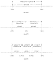
- the system 10 has a fixed range of frequencies 50, for example the range between 20kHz and 30kHz, as shown in Figures 2A-2C .
- the fixed range of frequencies 50 is generally selected by the user 46, and can be determined by the known or expected frequencies produced by the group of switching devices 38.
- the known or expected frequencies of the switching devices 38 can be provided by their manufacturer or determined from observations during operation of the switching devices 38.
- the bus addresses 42 have been assigned by the position of the switching devices 38 on the communication bus 26. Therefore, first switching device 14 has been assigned bus address 1, second switching device 18 has been assigned bus address 2 and third switching device 22 has been assigned bus address 3.
- the bus addresses 42 can also be assigned based on the known or expected frequencies of the switching devices 38 with respect to the fixed range of frequencies 50. For example, a switching device 38 known or expected to produce a switching frequency near the upper end of the fixed range of frequencies 50 could be assigned a higher bus address 42 than other switching devices 38 connected to the communications bus 26, regardless of its position on the communications bus 26.
- the fixed range of frequencies 50 is divided into equal subranges of frequencies 54, each subrange of frequencies 54 being associated with a unique bus address 42 and its associated switching device 38.
- the range of frequencies included in each subrange of frequencies 54 is determined by the range of frequencies in the fixed range of frequencies 50 and the number of switching devices 38 connected to the communications bus 26.
- first switching device 14 is connected to the communications bus 26.
- a subrange of frequencies 54 can be determined for each switching device 38 connected to the communications bus 26. Since the first switching device 14 is the only switching device 38 connected to the communications bus 26 in Figure 2A , it can access the full range of the fixed range of frequencies 50.
- the second switching device 18 is added to the communications bus 26, and the fixed range of frequencies 50 is divided into two equal subranges of frequencies 54, one for each of the first and second switching devices, 14 and 18 respectively.
- the third switching device 22 is added to the communications bus 26, and the fixed range of frequencies 50 is divided into three equal subranges of frequencies 54, one for each of the connected first, second and third switching devices, 14, 18 and 22 respectively.
- new switching devices 38 are added to the communications bus 26 new subranges of frequencies 54 will be created in the fixed range of frequencies 50.
- the range of frequencies in each of the subranges of frequencies 54 will automatically be reduced.
- the number of switching devices 38 connected to the communications bus 26 is decreased, the range of frequencies in each of the subranges of frequencies 54 will automatically be increased.
- the dynamic method can alter, in real time, all of the subranges of frequencies 54 within a fixed range of frequencies 50, in response to a change in any static or dynamic characteristic 58 of one or more of the switching devices 38 connected to the communications bus 26 and/or loads 106 controlled by the switching devices 38.
- the static characteristic 58 can include but are not limited to the type of switching device 38 (contactor, drive, power supply, etc.) and type of load 106 being controlled (motor etc.).
- the dynamic characteristics 58 can be sensed or calculated characteristics, which include but are not limited to the ON or OFF state of the switching device 38, a current level controlled by the switching device 38 (normal or high), voltage, power and, in some cases, the load 106 controlled by the switching device 38 (normal or heavy). These characteristics 58 are indicated in a table 62 by binary (0 or 1) weights 66 and, in some special cases where the characteristic 58 can include varying degrees (high, medium low, etc.), can include the numerals 2-9.
- the table 62 and algorithms 70 and 90 for processing information from the table 62 are stored in the non-transitory memory 74, the algorithms 70 and 90 being implemented by the processor 78.
- Algorithm 70 dynamically reduces the peak electromagnetic interference produced by switching devices 38 in the system 10 in real time.
- Algorithm 90 evaluates the weights 66 associated with each bus address 42 to determine a subrange of frequencies 54 for each bus address 42 and its associated switching device 38 connected to the communications bus 26.
- the algorithm 70 for dynamically reducing the peak electromagnetic interference produced by each switching device 38 in the system 10 and algorithm 90 for determining the subrange of frequencies 54 for each bus address 42 and its associated switching device 38 connected to the communications bus 26 will be explained in greater detail below.
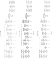
- Figures 3A-3C illustrate three example tables 62 for the first, second and third switching devices, 14, 18 and 22 respectively, of Figure 1 .
- Each example table 62 has a different configuration of characteristics 58 and their associated weights 66 for each of the first, second and third switching devices, 14, 18 and 22 respectively.
- bus address 1 (first switching device 14 ) is in an ON state, has a heavy load 106 and is a contactor. Therefore, address 1 has a total weighting 66 of 3.
- Bus address 2 (second switching device 18 ) is in an OFF state has a heavy load 106, high current and is a drive, but has a weighting 66 of zero because it is in an OFF state.
- Bus address 3 (third switching device 18 ) is in an ON state and is a power supply, and has a total weighting 66 of 2.
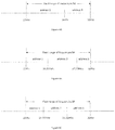
- the subranges of frequencies 54 for addresses 1, 2 and 3 are graphically illustrated in Figure 4A where the subrange of frequencies 54 for address 1 is 6Khz, the subrange of frequencies 54 for address 2 is 0Khz, and subrange of frequencies 54 for address 3 is 4Khz.
- addresses 1, 2 and 3 have the same characteristics 58 as in Figure 3A except that address 2 is now in an ON state and has a total weighting 66 of 4.
- the subrange of frequencies 54 for address 1 is now 3.333Khz
- the subrange of frequencies 54 for address 2 is now 4.444Khz
- the subrange of frequencies 54 for address 3 is now 2.222Khz.
- addresses 1 and 2 have the same characteristics 58 as in Figure 3B .
- address 3 now has characteristics 58 for a heavy load 106 and high current resulting in a total weighting 66 of 4.
- the subrange of frequencies 54 for address 1 is now 2.727Khz
- the subrange of frequencies 54 for address 2 is now 3.636Khz
- the subrange of frequencies 54 for address 3 is now 3.636Khz.
- a flow chart of the algorithm 70 for dynamically reducing the peak electromagnetic interference from a group of switching devices 38 is shown.
- a user 46 determines the minimum frequency 82 and maximum frequency 86 for the fixed range of frequencies 50 in which the group of switching devices 38 connected to the communications bus 26 will operate.
- the operating frequencies produced by the switching devices 38 is generally provided by the manufacturer or can be determined by monitoring the switching devices 38 during operation.
- the determined minimum 82 and maximum 86 frequencies are stored in table 62.
- the range of the fixed range of frequencies 50 can be adjusted by changing one or both of the minimum 82 and maximum 86 frequencies in table 62.
- the processor 78 detects the first switching device 38 on the communications bus 26.
- the processor determines if the detected switching device 38 has a unique bus address 42, if no unique bus address 42 is detected a unique bus address 42 will be assigned by the processor 78 or user 46.
- the unique bus address 42 associated with the detected switching device 38 is stored in table 62.
- the processor 78 detects and/or determines static and/or dynamic characteristics 58 of the detected switching device 38.
- the static and/or dynamic characteristics 58 are stored in table 62 such that they are associated with the unique bus address 42 of the detected switching device 38.
- the processor 78 determines if all of the switching devices 38 connected to the communications bus 26 have been detected and processed through steps 508 and 512. If the result of the determination at step 516 is NO, steps 504 through 516 are repeated until all switching devices 38 connected to the communications bus 26 have been processed. If the result of the determination at step 516 is YES, the processor 78 proceeds to step 520 where the subrange of frequencies 54 for each unique bus address 42 is determined and stored in table 62 such that each determined subrange of frequencies 54 is associated with its unique bus address.
- one of the processors 78 or 102 can determine the dithering duty cycle for each switching device 38 connected to the communications bus 26 by using the maximum frequency 110 and minimum frequency 114 of the subrange frequencies 54 associated with each switching device 38 connected to the communications bus 26.
- the dithering duty cycle can be determined by dividing the frequency of timer 98 associated with a particular switching device 38 by the maximum frequency 110 and/or minimum frequencies 114 of the subrange of frequencies 54 associated with that particular switching device 38.
- processor 78 scans table 62 for any changes to the switching device 38 characteristics 58 or bus addresses 42. At step 532, if no changes are discovered the processor 78 returns to step 524 of algorithm 70. If any changes to characteristics 58 or bus addresses 42 are discovered at step 528 the processor 78 returns to step 504 of algorithm 70.
- the range of the fixed range of frequency 50 is determined by subtracting the minimum frequency 82 stored in table 62 from maximum frequency 86 stored in table 62.
- the total number of weights 66 for each unique bus address 42 is determined. Any unique bus address 42 having an OFF state will have zero weights 66 since the total weighting 66 of each unique bus address 42 is determined by the sum of its weightings 66 times the weigh for its ON or OFF status. For example, in Figure 3A , address 2 has weightings 66 for a heavy load 106, high current and being a contactor but its status is OFF.
- the total number of weights 66 for all unique bus addresses 42 is determined by summing the total number of weights 66 for each unique bus address 42 in step 604.
- a frequency/weight range 94 is determined by dividing the determined range of frequencies for the fixed range of frequencies 50 from step 600 by the total number of weights 66 for all unique bus addresses 42 having an ON state in step 608.
- a subrange of frequencies 54 for each unique bus address 42 is determined by multiplying the total number of weights 66 for each unique bus address 42 by the frequency/weight range 94 and adding the product to highest frequency of the immediately lower subrange of frequencies 54.
- the determined frequency/weight range 94 is 1.111Khz per weight 66.
- This frequency/weight range 94 was determined by dividing the fixed range of frequencies 50 (10Khz) by the total number of weights 66 for all of the unique bus address 42 having an ON state (9 weights 66 ).
- the subrange of frequencies 54 starts at 20Khz (the minimum frequency 82 of fixed range of frequencies 50 ) and end at 23.333Khz ((3X1.111Khz) + 20Khz).
- the subrange of frequencies 54 for unique bus address 2 starts at 23.333Khz (highest frequency for the subrange of frequencies 54 of unique bus address 1) and end at 27.778Khz ((4X1.111Khz) + 23.333Khz).
- the subrange of frequencies 54 for unique bus address 3 starts at 27.778Khz (highest frequency for the subrange of frequencies 54 of unique bus address 2) and end at 30Khz, the highest frequency of the fixed range of frequencies 50 ((2X1.111Khz) + 27.778Khz).
- the determined subrange of frequencies 54 for each switching device 38 is stored in table 62 under the associated unique bus address 42.
Landscapes
- Engineering & Computer Science (AREA)
- Physics & Mathematics (AREA)
- Electromagnetism (AREA)
- Power Engineering (AREA)
- Microelectronics & Electronic Packaging (AREA)
- Computer Networks & Wireless Communication (AREA)
- Signal Processing (AREA)
- Control Of Ac Motors In General (AREA)
Abstract
Description
- The invention is generally directed to electrical or electronic switching devices and particularly to the intensity of the electromagnetic interference produced by multiple switching devices in a system.
- Systems having multiple electrical or electronic switching devices are common. These systems can include switching devices such as power supplies, drives, motor controllers, soft starters, protection devices or any electrical or electronic device that includes a switching element that can produce an electromagnetic signal during normal operation. If these switching devices are operating independently within the system, there is no means to coordinate switching frequencies between the individual devices in the system. Therefore, some devices may switch at the same frequency or at harmonics of other switching devices in the system, thereby concentrating electromagnetic emissions into a small frequency range(s), which causes a peak in electromagnetic emissions. These peak electromagnetic emissions can cause problems in other electronic devices or degrade their operating efficiency. Peak electromagnetic emissions may also exceed electromagnetic compatibility (EMC) regulations. Therefore, a relatively simple and inexpensive method of reducing the peak electromagnetic interference (EMI) produced by systems having multiple electrical or electronic switching device is desirable.
- The present invention provides a method for dynamically reducing the peak EMI produced by systems that have multiple electrical or electronic switching devices. The system includes:
- a controller having a microprocessor and a non-transitory memory associated with the microprocessor, the non-transitory memory storing an algorithm implemented by the microprocessor and characteristics of the switching devices and/or loads controlled by the switching devices;
- a fixed range of frequencies, the fixed range of frequencies including frequencies emitted by the group of switching devices during normal operation;
- a subrange of frequencies for each switching device in the group of switching devices, each subrange of frequencies being dynamically determined by the characteristics of its associated switching device and/or the load controlled by the switching device; and
- a timer associated with each switching device, the timer using a maximum and a minimum frequency of the subrange of frequencies associated with its associated switching device to spread the peak frequency of that associated switching device over its associated subrange of frequencies.
- a fixed range of frequencies, the fixed range of frequencies including frequencies emitted by the group of switching devices during normal operation;
- a subrange of frequencies associated with each switching device in the group of switching devices, each subrange of frequencies being dynamically determined by the characteristics of its associated switching device and/or the load controlled by its associated switching device; and
- a timer associated with each switching device, the timer using a maximum and a minimum frequency of the subrange of frequencies associated with its associated switching device to spread the peak frequency of that associated switching device over its associated subrange of frequencies.
- The invention also teaches a method for dynamically reducing a peak electromagnetic interference produced by a group of switching devices connected to a common communications bus, the method comprising:
- determining a fixed range of frequencies, the fixed range of frequencies including frequencies emitted by the group of switching devices during normal operation;
- determining, by a microprocessor, a subrange of frequencies associated with each switching device in the group of switching devices, each subrange of frequencies being dynamically determined by one or more characteristics of its associated switching device and/or a load controlled by its associated switching device; and
- spreading the peak frequency of each switching device over its associated subrange of frequencies by a timer associated with the switching device and using a maximum and a minimum frequency of the associated subrange of frequencies.
-
-
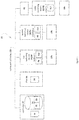
Figure 1 illustrates a typical system having a group of switching devices connected by a communications bus. -
Figures 2A-2C graphically illustrates a fixed range of frequencies with one to three subranges of frequencies defined by the switching device bus address. -
Figures 3A-3C illustrate tables used to dynamically determine the subranges of frequencies graphically illustrated inFigures 4A-4C . -
Figures 4A-4C graphically illustrates subranges of frequencies defined by the weights assigned to each switching device as shown in the table ofFigures 3A-3C . -
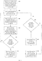
Figure 5 is a flow chart of the method for dynamically reducing the peak electromagnetic interference produced by the system. -
Figure 6 is a flow chart of the method for determining the range of frequencies for each subranges of frequencies in the fixed range of frequencies . - Referring now to
Figure 1 , a system for dynamically reducing the peak electromagnetic interference produced by a group of switching devices is generally indicated byreference number 10. Thesystem 10 includes first switching device 14, second switching device 18, and third switching device 22, each connected to acommunications bus 26. Acontroller 30, and/or a human machine interface (HMI) 34, can also be connected to thecommunications bus 26 but are not required for thesystem 10 to reduce the peak electromagnetic interference produced by a group of switching devices, collectively indicated byreference number 38. Anon-transitory memory 74 andprocessor 78 are shown in thecontroller 30, however, they can also be located in theHMI 34 or switchingdevices 38. Eachswitching device 38 also includes an associated timing device such as a clock, timer, oscillator or other means capable of providing evenly spaced intervals of time, generally indicated astimer 98. Thetimer 98 can be located in theswitching device 38 or between theprocessor 78 andswitching device 38. Theswitching devices 38 can also include abasic processor 102 for performing minor operations related toalgorithms system 10 is for the purpose of disclosing the present invention and does not limit or restrict the number of switchingdevices 38, in thesystem 10. Thecommunications bus 26 provides a means for communication between theswitching devices 38. Therefore, eachswitching device 38 is associated with a unique bus address 42. The bus addresses 42 can be any symbol or term that can be translated to a numeric value. It is also to be understood that the bus addresses 42 of switchingdevices 38 can be designed into theswitching devices 38 during manufacturing, manually set by switches or similar means on theswitching devices 38, determined by the position of theswitching devices 38 on thecommunication bus 26 or programed over thecommunications bus 26 by thecontroller 30 or a user 46 through theHMI 34. - The
system 10 has a fixed range offrequencies 50, for example the range between 20kHz and 30kHz, as shown inFigures 2A-2C . The fixed range offrequencies 50 is generally selected by the user 46, and can be determined by the known or expected frequencies produced by the group of switchingdevices 38. The known or expected frequencies of theswitching devices 38 can be provided by their manufacturer or determined from observations during operation of theswitching devices 38. In theexemplary system 10 ofFigure 1 , the bus addresses 42 have been assigned by the position of theswitching devices 38 on thecommunication bus 26. Therefore, first switching device 14 has been assignedbus address 1, second switching device 18 has been assignedbus address 2 and third switching device 22 has been assignedbus address 3. The bus addresses 42 can also be assigned based on the known or expected frequencies of theswitching devices 38 with respect to the fixed range offrequencies 50. For example, aswitching device 38 known or expected to produce a switching frequency near the upper end of the fixed range offrequencies 50 could be assigned a higher bus address 42 thanother switching devices 38 connected to thecommunications bus 26, regardless of its position on thecommunications bus 26. In this simple method for reducing the peak electromagnetic interference the fixed range offrequencies 50 is divided into equal subranges offrequencies 54, each subrange offrequencies 54 being associated with a unique bus address 42 and its associatedswitching device 38. The range of frequencies included in each subrange offrequencies 54 is determined by the range of frequencies in the fixed range offrequencies 50 and the number ofswitching devices 38 connected to thecommunications bus 26. In the example ofFigure 2A , only first switching device 14 is connected to thecommunications bus 26. Using only the switching devices' 38 bus addresses 42, a subrange offrequencies 54 can be determined for eachswitching device 38 connected to thecommunications bus 26. Since the first switching device 14 is theonly switching device 38 connected to thecommunications bus 26 inFigure 2A , it can access the full range of the fixed range offrequencies 50. InFigure 2B , the second switching device 18 is added to thecommunications bus 26, and the fixed range offrequencies 50 is divided into two equal subranges offrequencies 54, one for each of the first and second switching devices, 14 and 18 respectively. InFigure 2C , the third switching device 22 is added to thecommunications bus 26, and the fixed range offrequencies 50 is divided into three equal subranges offrequencies 54, one for each of the connected first, second and third switching devices, 14, 18 and 22 respectively. In this simple method of reducing peak electromagnetic interference, asnew switching devices 38 are added to thecommunications bus 26 new subranges offrequencies 54 will be created in the fixed range offrequencies 50. To maintain the determined fixed range offrequencies 50 as new subranges offrequencies 54 are created, the range of frequencies in each of the subranges offrequencies 54 will automatically be reduced. Alternatively, if the number ofswitching devices 38 connected to thecommunications bus 26 is decreased, the range of frequencies in each of the subranges offrequencies 54 will automatically be increased. - Referring now to
Figures 3A-3C , a method is disclosed for dynamically reducing the peak electromagnetic interference produced by thesystem 10. The dynamic method can alter, in real time, all of the subranges offrequencies 54 within a fixed range offrequencies 50, in response to a change in any static ordynamic characteristic 58 of one or more of theswitching devices 38 connected to thecommunications bus 26 and/orloads 106 controlled by theswitching devices 38. Thestatic characteristic 58 can include but are not limited to the type of switching device 38 (contactor, drive, power supply, etc.) and type ofload 106 being controlled (motor etc.). Thedynamic characteristics 58 can be sensed or calculated characteristics, which include but are not limited to the ON or OFF state of theswitching device 38, a current level controlled by the switching device 38 (normal or high), voltage, power and, in some cases, theload 106 controlled by the switching device 38 (normal or heavy). Thesecharacteristics 58 are indicated in a table 62 by binary (0 or 1)weights 66 and, in some special cases where the characteristic 58 can include varying degrees (high, medium low, etc.), can include the numerals 2-9. The table 62 andalgorithms non-transitory memory 74, thealgorithms processor 78.Algorithm 70 dynamically reduces the peak electromagnetic interference produced by switchingdevices 38 in thesystem 10 in real time.Algorithm 90 evaluates theweights 66 associated with each bus address 42 to determine a subrange offrequencies 54 for each bus address 42 and its associatedswitching device 38 connected to thecommunications bus 26. Thealgorithm 70 for dynamically reducing the peak electromagnetic interference produced by each switchingdevice 38 in thesystem 10 andalgorithm 90 for determining the subrange offrequencies 54 for each bus address 42 and its associatedswitching device 38 connected to thecommunications bus 26 will be explained in greater detail below. -
Figures 3A-3C illustrate three example tables 62 for the first, second and third switching devices, 14, 18 and 22 respectively, ofFigure 1 . Each example table 62 has a different configuration ofcharacteristics 58 and their associatedweights 66 for each of the first, second and third switching devices, 14, 18 and 22 respectively. InFigure 3A , bus address 1 (first switching device 14) is in an ON state, has aheavy load 106 and is a contactor. Therefore,address 1 has atotal weighting 66 of 3. Bus address 2 (second switching device 18) is in an OFF state has aheavy load 106, high current and is a drive, but has aweighting 66 of zero because it is in an OFF state. Bus address 3 (third switching device 18) is in an ON state and is a power supply, and has atotal weighting 66 of 2. The subranges offrequencies 54 foraddresses Figure 4A where the subrange offrequencies 54 foraddress 1 is 6Khz, the subrange offrequencies 54 foraddress 2 is 0Khz, and subrange offrequencies 54 foraddress 3 is 4Khz. InFigure 3B , addresses 1, 2 and 3 have thesame characteristics 58 as inFigure 3A except thataddress 2 is now in an ON state and has atotal weighting 66 of 4. As shown graphically inFigure 4B , the subrange offrequencies 54 foraddress 1 is now 3.333Khz, the subrange offrequencies 54 foraddress 2 is now 4.444Khz, and the subrange offrequencies 54 foraddress 3 is now 2.222Khz. InFigure 3C , addresses 1 and 2 have thesame characteristics 58 as inFigure 3B . However,address 3 now hascharacteristics 58 for aheavy load 106 and high current resulting in atotal weighting 66 of 4. As shown graphically inFigure 4C , the subrange offrequencies 54 foraddress 1 is now 2.727Khz, the subrange offrequencies 54 foraddress 2 is now 3.636Khz, and the subrange offrequencies 54 foraddress 3 is now 3.636Khz. - Referring now to
Figure 5 , a flow chart of thealgorithm 70 for dynamically reducing the peak electromagnetic interference from a group of switchingdevices 38 is shown. At step 500 a user 46 determines theminimum frequency 82 andmaximum frequency 86 for the fixed range offrequencies 50 in which the group of switchingdevices 38 connected to thecommunications bus 26 will operate. The operating frequencies produced by theswitching devices 38 is generally provided by the manufacturer or can be determined by monitoring theswitching devices 38 during operation. Thedetermined minimum 82 and maximum 86 frequencies are stored in table 62. Although it is not normally required, the range of the fixed range offrequencies 50 can be adjusted by changing one or both of the minimum 82 and maximum 86 frequencies in table 62. For example, the addition of aswitching device 38 that operates outside the current fixed range offrequencies 50 to thecommunications bus 26 or removal from thecommunications bus 26 of aswitching device 38 operating at theextreme minimum 82 ormaximum 86 of the fixed range offrequencies 50 can initiate a change in the fixed range offrequencies 50. Atstep 504, theprocessor 78 detects thefirst switching device 38 on thecommunications bus 26. Atstep 508 the processor determines if the detected switchingdevice 38 has a unique bus address 42, if no unique bus address 42 is detected a unique bus address 42 will be assigned by theprocessor 78 or user 46. The unique bus address 42 associated with the detected switchingdevice 38 is stored in table 62. Atstep 512, theprocessor 78 detects and/or determines static and/ordynamic characteristics 58 of the detected switchingdevice 38. The static and/ordynamic characteristics 58 are stored in table 62 such that they are associated with the unique bus address 42 of the detected switchingdevice 38. At step 516, theprocessor 78 determines if all of theswitching devices 38 connected to thecommunications bus 26 have been detected and processed throughsteps devices 38 connected to thecommunications bus 26 have been processed. If the result of the determination at step 516 is YES, theprocessor 78 proceeds to step 520 where the subrange offrequencies 54 for each unique bus address 42 is determined and stored in table 62 such that each determined subrange offrequencies 54 is associated with its unique bus address. The process for dynamically determining each subrange offrequencies 54 will be described in detail with respect toFigure 6 . Atstep 524, once the subrange offrequencies 54 for each switchingdevice 38 has been determined, one of theprocessors device 38 connected to thecommunications bus 26 by using the maximum frequency 110 and minimum frequency 114 of thesubrange frequencies 54 associated with each switchingdevice 38 connected to thecommunications bus 26. For example, the dithering duty cycle can be determined by dividing the frequency oftimer 98 associated with aparticular switching device 38 by the maximum frequency 110 and/or minimum frequencies 114 of the subrange offrequencies 54 associated with thatparticular switching device 38. This determines the number of ticks (half cycles) oftimer 98 over which the frequency of the timer's 98 associated switchingdevice 38 will be spread. Thetimer 98 then controls the ON time of its associatedswitching device 38 using the determined number of ticks. Atstep 528,processor 78 scans table 62 for any changes to theswitching device 38characteristics 58 or bus addresses 42. Atstep 532, if no changes are discovered theprocessor 78 returns to step 524 ofalgorithm 70. If any changes tocharacteristics 58 or bus addresses 42 are discovered atstep 528 theprocessor 78 returns to step 504 ofalgorithm 70. - Referring now to
Figure 6 , analgorithm 90 for dynamically determining the subranges offrequency 54 is described in detail. Atstep 600 the range of the fixed range offrequency 50 is determined by subtracting theminimum frequency 82 stored in table 62 frommaximum frequency 86 stored in table 62. Atstep 604 the total number ofweights 66 for each unique bus address 42 is determined. Any unique bus address 42 having an OFF state will have zeroweights 66 since thetotal weighting 66 of each unique bus address 42 is determined by the sum of itsweightings 66 times the weigh for its ON or OFF status. For example, inFigure 3A ,address 2 hasweightings 66 for aheavy load 106, high current and being a contactor but its status is OFF. Therefore, thetotal weightings 66 foraddress 2 would be 3X0=0. Atstep 608, the total number ofweights 66 for all unique bus addresses 42 is determined by summing the total number ofweights 66 for each unique bus address 42 instep 604. Atstep 612, a frequency/weight range 94 is determined by dividing the determined range of frequencies for the fixed range offrequencies 50 fromstep 600 by the total number ofweights 66 for all unique bus addresses 42 having an ON state instep 608. At step 616 a subrange offrequencies 54 for each unique bus address 42 is determined by multiplying the total number ofweights 66 for each unique bus address 42 by the frequency/weight range 94 and adding the product to highest frequency of the immediately lower subrange offrequencies 54. For example, inFigure 3B the determined frequency/weight range 94 is 1.111Khz perweight 66. This frequency/weight range 94 was determined by dividing the fixed range of frequencies 50 (10Khz) by the total number ofweights 66 for all of the unique bus address 42 having an ON state (9 weights 66). Forunique bus address 1 the subrange offrequencies 54 starts at 20Khz (theminimum frequency 82 of fixed range of frequencies 50) and end at 23.333Khz ((3X1.111Khz) + 20Khz). The subrange offrequencies 54 forunique bus address 2 starts at 23.333Khz (highest frequency for the subrange offrequencies 54 of unique bus address 1) and end at 27.778Khz ((4X1.111Khz) + 23.333Khz). The subrange offrequencies 54 forunique bus address 3 starts at 27.778Khz (highest frequency for the subrange offrequencies 54 of unique bus address 2) and end at 30Khz, the highest frequency of the fixed range of frequencies 50 ((2X1.111Khz) + 27.778Khz). Atstep 620 the determined subrange offrequencies 54 for each switchingdevice 38 is stored in table 62 under the associated unique bus address 42.
Claims (20)
- A system for reducing a peak electromagnetic interference produced by each switching device of a group of switching devices connected to a communications bus, the system comprising:a controller having a microprocessor and a non-transitory memory associated with the microprocessor, the non-transitory memory storing an algorithm implemented by the microprocessor and characteristics of the switching devices and/or loads controlled by the switching devices;a fixed range of frequencies, the fixed range of frequencies including frequencies emitted by the group of switching devices during normal operation;a subrange of frequencies associated with each switching device in the group of switching devices, each subrange of frequencies being dynamically determined by the characteristics of its associated switching device and/or the load controlled by its associated switching device; anda timer associated with each switching device, the timer using a maximum and a minimum frequency of the subrange of frequencies associated with its associated switching device to spread the peak frequency of that associated switching device over its associated subrange of frequencies.
- The system of claim 1, wherein the group of switching devices can include one or more of a power supply, a drive, a motor controller, a soft starter, a protective device or any electrical or electronic device that includes a switching element that can produce an electromagnetic signal during normal operation.
- The system of claim 1, wherein the fixed range of frequencies is determined by a user.
- The system of claim 1, wherein the total frequency range of all subranges of frequencies is contained within the fixed range of frequencies.
- The system of claim 1, wherein the peak electromagnet interference produced by the group of switching devices is reduced by reducing the overlap of frequencies produced by the individual switching devices of the group of switching devices.
- The system of claim 1, wherein the network address can be a numeric value or any symbol that can be converted to a numeric value.
- The system of claim 1, wherein the characteristic are indicated by a weight, which can be a binary value or a numeric value associated with one or both of a static characteristic of the switching device and/or the load controlled by the switching device or a dynamic characteristic of the switching device and/or the load controlled by the switching device.
- The system of claim 7, wherein the static characteristic can be a type of switching device or a type of load controlled by the switching device.
- The system of claim 7, wherein, the dynamic characteristics can be sensed or determined such as an On or an Off state of the switching device, a current, a voltage, a power, or ranges of the sensed or determined characteristics such as low, medium or high.
- The system of claim 1, wherein the characteristics of each switching device and/or load are continuously updated by the microprocessor.
- A method for dynamically reducing a peak electromagnetic interference produced by a group of switching devices connected to a common communications bus, the method comprising:determining a fixed range of frequencies, the fixed range of frequencies including frequencies emitted by the group of switching devices during normal operation;determining, by a microprocessor, a subrange of frequencies associated with each switching device in the group of switching devices, each subrange of frequencies being dynamically determined by one or more characteristics of its associated switching device and/or a load controlled by its associated switching device; andspreading the peak frequency of each switching device over its associated subrange of frequencies by a timer associated with the switching device and using a maximum and a minimum frequency of the associated subrange of frequencies.
- The method of claim 11, wherein the group of switching devices can include one or more of a power supply, a drive, a motor controller, a soft starter, a protective device or any electrical or electronic device that includes a switching element that can produce an electromagnetic signal during normal operation.
- The method of claim 11, wherein the fixed range of frequencies is determined by a user.
- The method of claim 11, wherein the total frequency range of all subranges of frequencies is contained within the fixed range of frequencies.
- The method of claim 11, wherein the network address can be a numeric value or any symbol that can be converted to a numeric value.
- The method of claim 11, wherein the characteristics are indicated by a weight that can be a numeric value associated with one or both of a static characteristic of the switching device or a dynamic characteristic of the switching device.
- The method of claim 16, wherein the static characteristic can be a type of switching device or a type of load controlled by the switching device.
- The method of claim 16, wherein, the dynamic characteristics can be sensed or determined such as an On or an Off state of the switching device, a current, a voltage, a power, or ranges of the sensed or determined characteristics such as low, medium or high.
- The method of claim 11, wherein the characteristics of each switching device and/or load are continuously updated by the microprocessor.
- The method of claim 11, wherein spreading the peak frequency of each switching device over its associated subrange of frequencies is accomplished by a timer associated with each switching device, the timer using a maximum and a minimum frequency of the subrange of frequencies associated with its associated switching device to spread the peak frequency of that associated switching device over its associated subrange of frequencies.
Applications Claiming Priority (1)
| Application Number | Priority Date | Filing Date | Title |
|---|---|---|---|
| US15/793,392 US10574137B2 (en) | 2017-10-25 | 2017-10-25 | Method for dynamically reducing peak electromagnetic interference from a group of switching devices connected on a communications bus |
Publications (1)
| Publication Number | Publication Date |
|---|---|
| EP3477836A1 true EP3477836A1 (en) | 2019-05-01 |
Family
ID=63965384
Family Applications (1)
| Application Number | Title | Priority Date | Filing Date |
|---|---|---|---|
| EP18202050.3A Pending EP3477836A1 (en) | 2017-10-25 | 2018-10-23 | System and method for dynamically reducing peak electromagnetic interference from a group of switching devices connected on a communications bus |
Country Status (2)
| Country | Link |
|---|---|
| US (1) | US10574137B2 (en) |
| EP (1) | EP3477836A1 (en) |
Citations (2)
| Publication number | Priority date | Publication date | Assignee | Title |
|---|---|---|---|---|
| US20140225435A1 (en) * | 2011-09-05 | 2014-08-14 | Toyota Jidosha Kabushiki Kaisha | Fuel cell system |
| US20160134326A1 (en) * | 2014-11-12 | 2016-05-12 | Hyundai Autron Co., Ltd. | Method and apparatus for controlling power source semiconductor |
Family Cites Families (4)
| Publication number | Priority date | Publication date | Assignee | Title |
|---|---|---|---|---|
| US6674789B1 (en) | 1999-09-17 | 2004-01-06 | Delphi Technologies, Inc. | Reduction of EMI through switching frequency dithering |
| US20040090802A1 (en) | 2002-11-01 | 2004-05-13 | Sierra Wireless, Inc., A Canadian Corporation | Noise suppression in switching power supplies |
| US20090086518A1 (en) * | 2007-09-29 | 2009-04-02 | Gordon Currie | Switching mode power supplies with digital electromagnetic interference control |
| US8767867B1 (en) | 2012-05-16 | 2014-07-01 | Cypress Semiconductor Corporation | Integrated control of power supply and power line communications |
-
2017
- 2017-10-25 US US15/793,392 patent/US10574137B2/en active Active
-
2018
- 2018-10-23 EP EP18202050.3A patent/EP3477836A1/en active Pending
Patent Citations (2)
| Publication number | Priority date | Publication date | Assignee | Title |
|---|---|---|---|---|
| US20140225435A1 (en) * | 2011-09-05 | 2014-08-14 | Toyota Jidosha Kabushiki Kaisha | Fuel cell system |
| US20160134326A1 (en) * | 2014-11-12 | 2016-05-12 | Hyundai Autron Co., Ltd. | Method and apparatus for controlling power source semiconductor |
Also Published As
| Publication number | Publication date |
|---|---|
| US20190124801A1 (en) | 2019-04-25 |
| US10574137B2 (en) | 2020-02-25 |
Similar Documents
| Publication | Publication Date | Title |
|---|---|---|
| CN105532073B (en) | Method and apparatus for determining the suitability of a cookware for a corresponding induction coil of an induction cooking range | |
| EP3413162B1 (en) | Control system and control method for ddr system | |
| CN113960384A (en) | Phase-loss detection method and device, storage medium and household equipment | |
| CN110446288A (en) | The acquisition methods and device of power adjusting factor | |
| CN114183902A (en) | Control method and device of air conditioner, air conditioner and computer readable storage medium | |
| EP2934064B1 (en) | Power management for home appliances | |
| EP2518853A1 (en) | Systems, methods, and apparatus for coordinated Volt/VAR control in power distribution networks | |
| EP2043240A2 (en) | Switching mode power supplies with digital electromagnetic interference control | |
| US10185295B2 (en) | Dynamic control of switching frequency in a switch mode power converter | |
| US10574137B2 (en) | Method for dynamically reducing peak electromagnetic interference from a group of switching devices connected on a communications bus | |
| CN109600977B (en) | Heat dissipation control method and electronic equipment | |
| EP3327918B1 (en) | Power conversion device and method for reducing output current noise therefrom | |
| CN112557740B (en) | Method and device for avoiding zero-crossing signal detection time deviation in zero-crossing detection circuit | |
| CN109883020A (en) | Control method and device of air conditioner, storage medium and air conditioner | |
| EP3764740A1 (en) | Method for controlling an induction cooking hob | |
| CN109524967B (en) | Load operation control method and power grid system | |
| CN109768756A (en) | Motor control method and device, motor and computer readable storage medium | |
| CN110262321A (en) | A kind of control method of food processor | |
| CN117641635A (en) | Drive control method, drive control device, electromagnetic heating device and storage medium | |
| KR20250123169A (en) | Control method, device and electromagnetic heating circuit for electromagnetic heating circuit | |
| US7102324B2 (en) | Fixed speed drive | |
| US9083315B2 (en) | Circuit configuration for eliminating EMC interference | |
| KR102140951B1 (en) | Power supply apparatus and air conditioner including the same | |
| CN115459571B (en) | Magnetic ring overheat protection method, system, device, equipment and medium | |
| EP3206098B1 (en) | Systems and methods for implementing multiple motor control modes in a motor drive controller |
Legal Events
| Date | Code | Title | Description |
|---|---|---|---|
| PUAI | Public reference made under article 153(3) epc to a published international application that has entered the european phase |
Free format text: ORIGINAL CODE: 0009012 |
|
| STAA | Information on the status of an ep patent application or granted ep patent |
Free format text: STATUS: THE APPLICATION HAS BEEN PUBLISHED |
|
| AK | Designated contracting states |
Kind code of ref document: A1 Designated state(s): AL AT BE BG CH CY CZ DE DK EE ES FI FR GB GR HR HU IE IS IT LI LT LU LV MC MK MT NL NO PL PT RO RS SE SI SK SM TR |
|
| AX | Request for extension of the european patent |
Extension state: BA ME |
|
| STAA | Information on the status of an ep patent application or granted ep patent |
Free format text: STATUS: REQUEST FOR EXAMINATION WAS MADE |
|
| 17P | Request for examination filed |
Effective date: 20191104 |
|
| RBV | Designated contracting states (corrected) |
Designated state(s): AL AT BE BG CH CY CZ DE DK EE ES FI FR GB GR HR HU IE IS IT LI LT LU LV MC MK MT NL NO PL PT RO RS SE SI SK SM TR |
|
| STAA | Information on the status of an ep patent application or granted ep patent |
Free format text: STATUS: EXAMINATION IS IN PROGRESS |
|
| 17Q | First examination report despatched |
Effective date: 20210623 |