EP3477686A1 - Semiconductor device and semiconductor integrated circuit - Google Patents
Semiconductor device and semiconductor integrated circuit Download PDFInfo
- Publication number
- EP3477686A1 EP3477686A1 EP16907234.5A EP16907234A EP3477686A1 EP 3477686 A1 EP3477686 A1 EP 3477686A1 EP 16907234 A EP16907234 A EP 16907234A EP 3477686 A1 EP3477686 A1 EP 3477686A1
- Authority
- EP
- European Patent Office
- Prior art keywords
- gate electrodes
- transistors
- gate electrode
- gate
- transistor
- Prior art date
- Legal status (The legal status is an assumption and is not a legal conclusion. Google has not performed a legal analysis and makes no representation as to the accuracy of the status listed.)
- Withdrawn
Links
Images




Classifications
-
- H—ELECTRICITY
- H10—SEMICONDUCTOR DEVICES; ELECTRIC SOLID-STATE DEVICES NOT OTHERWISE PROVIDED FOR
- H10D—INORGANIC ELECTRIC SEMICONDUCTOR DEVICES
- H10D30/00—Field-effect transistors [FET]
- H10D30/60—Insulated-gate field-effect transistors [IGFET]
-
- H—ELECTRICITY
- H10—SEMICONDUCTOR DEVICES; ELECTRIC SOLID-STATE DEVICES NOT OTHERWISE PROVIDED FOR
- H10D—INORGANIC ELECTRIC SEMICONDUCTOR DEVICES
- H10D30/00—Field-effect transistors [FET]
- H10D30/60—Insulated-gate field-effect transistors [IGFET]
- H10D30/62—Fin field-effect transistors [FinFET]
-
- H—ELECTRICITY
- H10—SEMICONDUCTOR DEVICES; ELECTRIC SOLID-STATE DEVICES NOT OTHERWISE PROVIDED FOR
- H10D—INORGANIC ELECTRIC SEMICONDUCTOR DEVICES
- H10D30/00—Field-effect transistors [FET]
- H10D30/60—Insulated-gate field-effect transistors [IGFET]
- H10D30/62—Fin field-effect transistors [FinFET]
- H10D30/6211—Fin field-effect transistors [FinFET] having fin-shaped semiconductor bodies integral with the bulk semiconductor substrates
-
- H—ELECTRICITY
- H10—SEMICONDUCTOR DEVICES; ELECTRIC SOLID-STATE DEVICES NOT OTHERWISE PROVIDED FOR
- H10D—INORGANIC ELECTRIC SEMICONDUCTOR DEVICES
- H10D62/00—Semiconductor bodies, or regions thereof, of devices having potential barriers
- H10D62/10—Shapes, relative sizes or dispositions of the regions of the semiconductor bodies; Shapes of the semiconductor bodies
- H10D62/113—Isolations within a component, i.e. internal isolations
-
- H—ELECTRICITY
- H10—SEMICONDUCTOR DEVICES; ELECTRIC SOLID-STATE DEVICES NOT OTHERWISE PROVIDED FOR
- H10D—INORGANIC ELECTRIC SEMICONDUCTOR DEVICES
- H10D62/00—Semiconductor bodies, or regions thereof, of devices having potential barriers
- H10D62/10—Shapes, relative sizes or dispositions of the regions of the semiconductor bodies; Shapes of the semiconductor bodies
- H10D62/13—Semiconductor regions connected to electrodes carrying current to be rectified, amplified or switched, e.g. source or drain regions
- H10D62/149—Source or drain regions of field-effect devices
- H10D62/151—Source or drain regions of field-effect devices of IGFETs
-
- H—ELECTRICITY
- H10—SEMICONDUCTOR DEVICES; ELECTRIC SOLID-STATE DEVICES NOT OTHERWISE PROVIDED FOR
- H10D—INORGANIC ELECTRIC SEMICONDUCTOR DEVICES
- H10D64/00—Electrodes of devices having potential barriers
- H10D64/20—Electrodes characterised by their shapes, relative sizes or dispositions
- H10D64/23—Electrodes carrying the current to be rectified, amplified, oscillated or switched, e.g. sources, drains, anodes or cathodes
- H10D64/251—Source or drain electrodes for field-effect devices
- H10D64/257—Source or drain electrodes for field-effect devices for lateral devices wherein the source or drain electrodes are characterised by top-view geometrical layouts, e.g. interdigitated, semi-circular, annular or L-shaped electrodes
-
- H—ELECTRICITY
- H10—SEMICONDUCTOR DEVICES; ELECTRIC SOLID-STATE DEVICES NOT OTHERWISE PROVIDED FOR
- H10D—INORGANIC ELECTRIC SEMICONDUCTOR DEVICES
- H10D64/00—Electrodes of devices having potential barriers
- H10D64/20—Electrodes characterised by their shapes, relative sizes or dispositions
- H10D64/27—Electrodes not carrying the current to be rectified, amplified, oscillated or switched, e.g. gates
- H10D64/311—Gate electrodes for field-effect devices
- H10D64/411—Gate electrodes for field-effect devices for FETs
- H10D64/511—Gate electrodes for field-effect devices for FETs for IGFETs
- H10D64/512—Disposition of the gate electrodes, e.g. buried gates
-
- H—ELECTRICITY
- H10—SEMICONDUCTOR DEVICES; ELECTRIC SOLID-STATE DEVICES NOT OTHERWISE PROVIDED FOR
- H10D—INORGANIC ELECTRIC SEMICONDUCTOR DEVICES
- H10D64/00—Electrodes of devices having potential barriers
- H10D64/20—Electrodes characterised by their shapes, relative sizes or dispositions
- H10D64/27—Electrodes not carrying the current to be rectified, amplified, oscillated or switched, e.g. gates
- H10D64/311—Gate electrodes for field-effect devices
- H10D64/411—Gate electrodes for field-effect devices for FETs
- H10D64/511—Gate electrodes for field-effect devices for FETs for IGFETs
- H10D64/517—Gate electrodes for field-effect devices for FETs for IGFETs characterised by the conducting layers
- H10D64/519—Gate electrodes for field-effect devices for FETs for IGFETs characterised by the conducting layers characterised by their top-view geometrical layouts
-
- H—ELECTRICITY
- H10—SEMICONDUCTOR DEVICES; ELECTRIC SOLID-STATE DEVICES NOT OTHERWISE PROVIDED FOR
- H10D—INORGANIC ELECTRIC SEMICONDUCTOR DEVICES
- H10D84/00—Integrated devices formed in or on semiconductor substrates that comprise only semiconducting layers, e.g. on Si wafers or on GaAs-on-Si wafers
- H10D84/80—Integrated devices formed in or on semiconductor substrates that comprise only semiconducting layers, e.g. on Si wafers or on GaAs-on-Si wafers characterised by the integration of at least one component covered by groups H10D12/00 or H10D30/00, e.g. integration of IGFETs
- H10D84/82—Integrated devices formed in or on semiconductor substrates that comprise only semiconducting layers, e.g. on Si wafers or on GaAs-on-Si wafers characterised by the integration of at least one component covered by groups H10D12/00 or H10D30/00, e.g. integration of IGFETs of only field-effect components
- H10D84/83—Integrated devices formed in or on semiconductor substrates that comprise only semiconducting layers, e.g. on Si wafers or on GaAs-on-Si wafers characterised by the integration of at least one component covered by groups H10D12/00 or H10D30/00, e.g. integration of IGFETs of only field-effect components of only insulated-gate FETs [IGFET]
- H10D84/85—Complementary IGFETs, e.g. CMOS
- H10D84/853—Complementary IGFETs, e.g. CMOS comprising FinFETs
-
- H—ELECTRICITY
- H10—SEMICONDUCTOR DEVICES; ELECTRIC SOLID-STATE DEVICES NOT OTHERWISE PROVIDED FOR
- H10D—INORGANIC ELECTRIC SEMICONDUCTOR DEVICES
- H10D84/00—Integrated devices formed in or on semiconductor substrates that comprise only semiconducting layers, e.g. on Si wafers or on GaAs-on-Si wafers
- H10D84/01—Manufacture or treatment
- H10D84/0123—Integrating together multiple components covered by H10D12/00 or H10D30/00, e.g. integrating multiple IGBTs
- H10D84/0126—Integrating together multiple components covered by H10D12/00 or H10D30/00, e.g. integrating multiple IGBTs the components including insulated gates, e.g. IGFETs
- H10D84/0135—Manufacturing their gate conductors
-
- H—ELECTRICITY
- H10—SEMICONDUCTOR DEVICES; ELECTRIC SOLID-STATE DEVICES NOT OTHERWISE PROVIDED FOR
- H10D—INORGANIC ELECTRIC SEMICONDUCTOR DEVICES
- H10D84/00—Integrated devices formed in or on semiconductor substrates that comprise only semiconducting layers, e.g. on Si wafers or on GaAs-on-Si wafers
- H10D84/01—Manufacture or treatment
- H10D84/02—Manufacture or treatment characterised by using material-based technologies
- H10D84/03—Manufacture or treatment characterised by using material-based technologies using Group IV technology, e.g. silicon technology or silicon-carbide [SiC] technology
- H10D84/038—Manufacture or treatment characterised by using material-based technologies using Group IV technology, e.g. silicon technology or silicon-carbide [SiC] technology using silicon technology, e.g. SiGe
Definitions
- the present invention relates to a semiconductor device and a semiconductor integrated circuit.
- Some field effect transistors have a fin-shaped structure (Fin Field Effect Transistor: FinFET) in which a gate insulating film and a gate electrode are formed on both side surfaces and a top surface of part of a projecting (fin-shaped) semiconductor region which is formed on a substrate to extend in one direction, and a source region and a drain region are formed in the projecting semiconductor region on both sides of the gate electrode (refer to Patent Literature 1, for instance). Since a FinFET is likely to be filled with heat because of its structure, some means to reduce heat generation by layout needs to be devised.
- FinFET Fin Field Effect Transistor
- FIG. 8 is a view illustrating a structure example of the FinFET having a multi-finger structure in which a plurality of gate electrodes are formed in a comb-teeth shape (finger shape).
- 101 denotes projecting (fin-shaped) semiconductor regions formed on a substrate to extend in one direction.
- gate electrodes 102 covering their both side surfaces and top surfaces with gate insulating films therebetween are formed so as to intersect with the projecting semiconductor regions 101, and source regions and drain regions arc formed in the projecting semiconductor regions 101 on both sides of the gate electrodes 102.
- the gate electrodes 102 are formed of, for example, polysilicon and are connected to a metal wiring line 103 through vias.
- 104 denotes element isolation insulating film (Shallow Trench Isolation: STI) for isolating a transistor forming region
- 105 denotes dummy gate electrode which is disposed between the gate electrode 102 and STI 104 and are formed on the same layer as that of the gate electrodes 102.
- the dummy gate electrodes 102 are also formed of, for example, polysilicon.
- the FinFET having the multi-finger structure is more likely to generate heat as the number of fingers is larger due to the influence of heat generation of adjacent transistors. That is, the FinFET having the multi-finger structure illustrated in FIG. 8 is more likely to generate heat than the FinFET where the number of fingers is 1.
- FIG. 10 is a view illustrating a structure example of the FinFET where the number of fingers is 1, and the same constituent elements as the constituent elements illustrated in FIG. 8 are denoted by the same reference numerals.
- the distance x between STIs 104 disposed at both sides of gate electrode 102 is short.
- an increase in the number of transistors is required, leading to an increase in power consumption and the area.
- Patent Literature 1 Japanese Laid-open Patent Publication No. 2015-220420
- a semiconductor device in one embodiment includes: element isolation regions; a projecting semiconductor region; a plurality of first gate electrodes each formed on both side surfaces and a top surface of a portion of the projecting semiconductor region, the plurality of first gate electrodes being formed between a pair of opposed end portions of the element isolation regions; a second gate electrode formed between the first gate electrodes, in the same layer as a layer where the plurality of first gate electrodes are formed, and applied with a voltage for turning off a transistor; and source regions and drain regions formed in the projecting semiconductor region at both sides of the first gate electrodes and the second gate electrode.
- a transistor including the second gate electrode applied with the voltage for turning off the transistors is disposed, thereby enabling a reduction in heat generation in the transistors without reducing a saturation current of the transistors.
- FIG. 1 is a view illustrating a structure example of a field effect transistor having a fin-shaped structure (Fin Field Effect Transistor: FinFET) as a semiconductor device in one embodiment of the present invention.
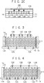
- FIG. 2A is a schematic sectional view along the I-I line in FIG. 1
- FIG. 2B is a schematic sectional view along the II-II line in FIG. 1
- FIG. 2C is a schematic sectional view along the III-III line in FIG. 1 .
- projecting (fin-shaped) semiconductor regions 11 extending in one direction are formed on a substrate 17.
- not-illustrated gate insulating films are formed on their both side surfaces and top surfaces.
- gate electrodes 12A, 12B covering the both side surfaces and the top surfaces are formed with the gate insulating films therebetween.
- Source regions and drain regions are formed in the projecting semiconductor regions 11 at both sides of the gate insulating film-covered portions of the projecting semiconductor regions 11, in other words, at both sides of the gate electrodes 12A, 12B.
- the gate electrodes 12A, 12B are formed in the same layer, between a pair of opposed end portions of element isolation regions, and are made of, for example, polysilicon.
- the gate electrodes 12A are connected through vias 16A to a metal wiring line 13A to which a signal is input.
- the gate electrodes 12B are connected through vias 16B to a metal wiring line 13B to which the same voltage as that of a back gate is applied.
- the source regions and the drain regions formed in the projecting semiconductor regions 11 are connected to source electrodes and drain electrodes respectively, through not-illustrated contact electrodes.
- element isolation insulating films 14 (Shallow Trench Isolation: STI) 14 for isolating a transistor-forming region are formed on the substrate 17.
- Dummy gate electrodes 15 made of, for example, polysilicon, are each formed between STI 14 and the gate electrode 12A or 12B, in the same layer as that of the gate electrodes 12A, 12B.
- the semiconductor device illustrated in FIG. 1, FIG. 2A, FIG. 2B , and FIG. 2C can be formed using a known manufacturing method, and can be formed using, for example, at least part of the manufacturing method described in the aforesaid Patent Literature 1.
- the FinFET in this embodiment has a multi-finger structure in which the plurality of gate electrodes 12A to which a signal is applied are formed in a comb-teeth shape (finger shape) between the pair of opposed end portions of the element isolation regions on which STIs 14 are disposed, and the gate electrodes 12B applied with the same voltage as that of the back gate are each disposed between the gate electrodes 12A to which a signal is applied. That is, transistors MB in which the potential of the gate electrodes 12B is clipped so as to produce an off state are each disposed between transistors MA driven according to a signal.
- the distance between STIs 14 formed at both sides of the gate electrodes is sufficiently long, making it possible to alleviate STI stress to maintain a saturation current Ion.
- the gate electrodes 12A to which a signal is input and the gate electrodes 12B applied with the same voltage as that of the back gate are alternately provided. That is, between the transistors driven according to a signal, the single transistor in which the potential of the gate electrode is clipped so as to produce the off state is provided.
- the present invention is not limited to this.
- any number of the gate electrodes 12B applied with the same voltage as that of the back gate may be provided between each pair of the gate electrodes 12A to which a signal is input, and as illustrated in, for example, FIG. 3 , two of the gate electrodes 12B applied with the same voltage as that of the back gate may be provided between each pair of the gate electrodes 12A to which a signal is input. That is, two of the transistors in which the potential of the gate electrodes is clipped so as to produce the off state may be provided between each pair of the transistors driven according to the signal.
- the gate electrodes 12A to which a signal is input may be arranged in sets of adjacent two, and between the sets, the single gate electrode 12B applied with the same voltage as that of the back gate may be provided. That is, the transistors driven according to a signal may be arranged in sets of adjacent two, and between the sets, the single transistor in which the potential of the gate electrode is clipped so as to produce the off state may be provided.
- the gate electrodes 12A to which the signal is input may be arranged in sets of adjacent two, and between the sets, two of the gate electrodes 12B applied with the same voltage as that of the back gate may be provided. That is, the transistors driven according to a signal may be arranged in sets of adjacent two, and between the sets, two of the transistors in which the potential of the gate electrodes is clipped so as to produce the off state may be provided.
- the number of the adjacently arranged transistors driven according to a signal is preferably not more than two.
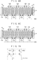
- FIG. 6A is a circuit diagram illustrating a configuration example of a voltage-controlled oscillation circuit (VCO) as an application example of the FinFET in this embodiment.
- the voltage-controlled oscillation circuit includes P-channel transistors M11, M13, N-channel transistors M12, M14, an inductor L11, a capacitor C11, and a voltage-controlled variable capacitor C12.
- the P-channel transistor M11 has a source connected to a signal line which supplies a power supply voltage VDD and has a drain connected to a drain of the N-channel transistor M12.
- the N-channel transistor M12 has a source connected to a signal line which supplies a reference voltage (for example, ground GND).
- the P-channel transistor M13 has a source connected to the signal line which supplies the power supply voltage VDD and has a drain connected to a drain of the N-channel transistor M14.
- the N-channel transistor M14 has a source connected to the signal line which supplies the reference voltage.
- a gate of the P-channel transistor M11 and a gate of the N-channel transistor M12 are connected to an interconnection point of the drain of the P-channel transistor M13 and the drain of the N-channel transistor M14.
- a gate of the P-channel transistor M13 and a gate of the N-channel transistor M14 are connected to an interconnection point of the drain of the P-channel transistor M11 and the drain of the N-channel transistor M12. That is, a first inverter constituted by the transistors M11, M12 and a second inverter constituted by the transistors M13, M14 are cross-coupled.
- the inductor L11, the capacitor C11, and the variable capacitor C12 are connected in parallel.
- the inductor L11 or the capacitance C11 is reduced, but too small an inductor L11 makes the oscillation difficult, and accordingly, the capacitance C11 is usually reduced.
- Dominant components of the capacitance C11 are a parasitic load of wiring and a load of the cross-coupled transistors. Further, since an oscillation signal has a sine wave, an on-period of the transistors M11 to M14 is relatively long, which tends to cause heat generation. Here, if an attempt is made to reduce the heat generation by, for example, the method illustrated in FIG. 10 , the load by the wiring increases and the saturation current Ion of the transistors reduces, necessitating an increase in the number of transistors. As a result, the capacitance C11 increases, making it difficult to achieve a desired oscillation frequency.
- the use of the FinFET in this embodiment as the transistors M11 to M14 enables to reduce the heat generation without reducing the saturation current Ion of the transistors, making it possible to inhibit an increase in the capacitance C11 due to the wiring load and to output a signal with a desired oscillation frequency.
- FIG. 6B and FIG. 6C are views illustrating structure examples of the P-channel transistors M11, M13 and the N-channel transistors M12, M14 illustrated in FIG. 6A , respectively, and the same constituent elements as the constituent elements illustrated in FIG. 1 are denoted by the same reference signs.
- source regions are each formed in the semiconductor region 11 between the gate electrode 12A and the gate electrode 12B (or the dummy gate electrode 15), and drain regions are each formed in the semiconductor region 11 between the adjacent gate electrodes 12A.
- the source regions are connected through not-illustrated contact electrodes to source electrodes to which the power supply voltage VDD is supplied, and the drain regions are connected to drain electrodes through not-illustrated contact electrodes.
- source regions are each formed in the semiconductor region 11 between the gate electrode 12A and the gate electrode 12B (or the dummy gate electrode 15), and drain regions are each formed in the semiconductor region 11 between the adjacent gate electrodes 12A.
- the source regions are connected through not-illustrated contact electrodes to source electrodes to which a reference voltage (for example, ground GND) is supplied, and the drain regions are connected to drain electrodes through not-illustrated contact electrodes.
- FIG. 7A is a circuit diagram illustrating a configuration example of a bias circuit as an application example of the FinFET in this embodiment.
- the bias circuit illustrated in FIG. 7A is a circuit in which P-channel transistors M21, M22 are current-mirror connected and a current twice a current L1 passes as a current 12.
- FIG. 7B is a view illustrating a structure example of the P-channel transistors M21, M22 illustrated in FIG. 7A , and the same constituent elements as the constituent elements illustrated in FIG. 1 are denoted by the same reference signs.
- the P-channel transistor M21 a transistor having a set of the two adjacent gate electrodes 12A is used, and as the P-channel transistor M22, two sets of the two adjacent gate electrodes 12A is used, which makes it possible to pass, as the current 12, a current twice the current I1 flowing in the transistor M21.
- a transistor including a gate electrode applied with a voltage for turning off the transistors is disposed, which makes it possible to reduce the heat generation in the transistors without decreasing the saturation current of the transistors.
Landscapes
- Metal-Oxide And Bipolar Metal-Oxide Semiconductor Integrated Circuits (AREA)
- Semiconductor Integrated Circuits (AREA)
- Insulated Gate Type Field-Effect Transistor (AREA)
Abstract
Description
- The present invention relates to a semiconductor device and a semiconductor integrated circuit.
- Some field effect transistors have a fin-shaped structure (Fin Field Effect Transistor: FinFET) in which a gate insulating film and a gate electrode are formed on both side surfaces and a top surface of part of a projecting (fin-shaped) semiconductor region which is formed on a substrate to extend in one direction, and a source region and a drain region are formed in the projecting semiconductor region on both sides of the gate electrode (refer to
Patent Literature 1, for instance). Since a FinFET is likely to be filled with heat because of its structure, some means to reduce heat generation by layout needs to be devised. -
FIG. 8 is a view illustrating a structure example of the FinFET having a multi-finger structure in which a plurality of gate electrodes are formed in a comb-teeth shape (finger shape). InFIG. 8 , 101 denotes projecting (fin-shaped) semiconductor regions formed on a substrate to extend in one direction. - In portions of the projecting
semiconductor regions 101,gate electrodes 102 covering their both side surfaces and top surfaces with gate insulating films therebetween are formed so as to intersect with the projectingsemiconductor regions 101, and source regions and drain regions arc formed in the projectingsemiconductor regions 101 on both sides of thegate electrodes 102. Thegate electrodes 102 are formed of, for example, polysilicon and are connected to ametal wiring line 103 through vias. - Further, in
FIG. 8 , 104 denotes element isolation insulating film (Shallow Trench Isolation: STI) for isolating a transistor forming region, and 105 denotes dummy gate electrode which is disposed between thegate electrode 102 andSTI 104 and are formed on the same layer as that of thegate electrodes 102. Thedummy gate electrodes 102 are also formed of, for example, polysilicon. - As illustrated in
FIG. 9 , the FinFET having the multi-finger structure is more likely to generate heat as the number of fingers is larger due to the influence of heat generation of adjacent transistors. That is, the FinFET having the multi-finger structure illustrated inFIG. 8 is more likely to generate heat than the FinFET where the number of fingers is 1. - One possible method to reduce the heat generation of the FinFET is a method to set the number of fingers to, for example, 1 as illustrated in
FIG. 10 to decrease the influence of the heat generation from adjacent .transistors, thereby reducing the heat generation.FIG. 10 is a view illustrating a structure example of the FinFET where the number of fingers is 1, and the same constituent elements as the constituent elements illustrated inFIG. 8 are denoted by the same reference numerals. - However, in the FinFET where the number of fingers is 1 as illustrated in
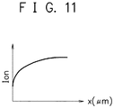
FIG. 10 , the distance x betweenSTIs 104 disposed at both sides ofgate electrode 102 is short. The shorter the distance x betweenSTIs 104 is, the lower a saturation current Ion of the transistor is, as illustrated inFIG. 11 due to STI stress (stress by STIs 104). Accordingly, in order to obtain the same saturation current Ion as that of the FinFET having the multi-finger structure illustrated in, for example,FIG. 8 , an increase in the number of transistors is required, leading to an increase in power consumption and the area. - Patent Literature 1: Japanese Laid-open Patent Publication No.
2015-220420 - It is an object of the present invention to provide a semiconductor device applied the FinFET achieving a reduction in heat generation in a transistor without reducing a saturation current of the transistor.
- A semiconductor device in one embodiment includes: element isolation regions; a projecting semiconductor region; a plurality of first gate electrodes each formed on both side surfaces and a top surface of a portion of the projecting semiconductor region, the plurality of first gate electrodes being formed between a pair of opposed end portions of the element isolation regions; a second gate electrode formed between the first gate electrodes, in the same layer as a layer where the plurality of first gate electrodes are formed, and applied with a voltage for turning off a transistor; and source regions and drain regions formed in the projecting semiconductor region at both sides of the first gate electrodes and the second gate electrode.
- In the disclosed semiconductor device, between transistors each including the first gate electrode, a transistor including the second gate electrode applied with the voltage for turning off the transistors is disposed, thereby enabling a reduction in heat generation in the transistors without reducing a saturation current of the transistors.
-
-
FIG. 1 is a view illustrating a structure example of a semiconductor device in this embodiment; -
FIG. 2A is a schematic sectional view along the I-I line inFIG. 1 ; -
FIG. 2B is a schematic sectional view along the II-II line inFIG. 1 ; -
FIG. 2C is a schematic sectional view along the III-III line inFIG. 1 ; -
FIG. 3 is a view illustrating another structure example of the semiconductor device in this embodiment; -
FIG. 4 is a view illustrating another structure example of the semiconductor device in this embodiment; -
FIG. 5 is a view illustrating another structure example of the semiconductor device in this embodiment; -
FIG. 6A is a circuit diagram illustrating a configuration example of an oscillation circuit which is an application example of the semiconductor device in this embodiment; -
FIG. 6B is a view illustrating a structure example of P-channel transistors illustrated inFIG. 6A ; -
FIG. 6C is a view illustrating a structure example of N-channel transistors illustrated inFIG. 6A ; -
FIG. 7A is a circuit diagram illustrating a configuration example of a bias circuit which is an application example of the semiconductor device in this embodiment; -
FIG. 7B is a view illustrating a structure example of transistors illustrated inFIG. 7A ; -
FIG. 8 is a view illustrating a structure example of a FinFET having a multi-finger structure; -
FIG. 9 is a chart illustrating a change in heat generation in accordance with the number of fingers in a FinFET; -
FIG. 10 is an explanatory view of a method to reduce heat generation of a FinFET; -
FIG. 11 is a chart illustrating a change in saturation current according to the distance between STIs in a FinFET. - Hereinafter, an embodiment of the present invention will be described based on the drawings.
-
FIG. 1 is a view illustrating a structure example of a field effect transistor having a fin-shaped structure (Fin Field Effect Transistor: FinFET) as a semiconductor device in one embodiment of the present invention.FIG. 2A is a schematic sectional view along the I-I line inFIG. 1, FIG. 2B is a schematic sectional view along the II-II line inFIG. 1 , andFIG. 2C is a schematic sectional view along the III-III line inFIG. 1 . - In the FinFET in this embodiment, projecting (fin-shaped)
semiconductor regions 11 extending in one direction are formed on asubstrate 17. In portions of the projectingsemiconductor regions 11, not-illustrated gate insulating films are formed on their both side surfaces and top surfaces. In the portions of the projectingsemiconductor regions 11,gate electrodes semiconductor regions 11 at both sides of the gate insulating film-covered portions of the projectingsemiconductor regions 11, in other words, at both sides of thegate electrodes - The
gate electrodes gate electrodes 12A are connected throughvias 16A to ametal wiring line 13A to which a signal is input. Thegate electrodes 12B are connected throughvias 16B to ametal wiring line 13B to which the same voltage as that of a back gate is applied. Further, the source regions and the drain regions formed in the projectingsemiconductor regions 11 are connected to source electrodes and drain electrodes respectively, through not-illustrated contact electrodes. - Further, element isolation insulating films 14 (Shallow Trench Isolation: STI) 14 for isolating a transistor-forming region are formed on the
substrate 17.Dummy gate electrodes 15 made of, for example, polysilicon, are each formed betweenSTI 14 and thegate electrode gate electrodes FIG. 1, FIG. 2A, FIG. 2B , andFIG. 2C can be formed using a known manufacturing method, and can be formed using, for example, at least part of the manufacturing method described in theaforesaid Patent Literature 1. - As described above, the FinFET in this embodiment has a multi-finger structure in which the plurality of
gate electrodes 12A to which a signal is applied are formed in a comb-teeth shape (finger shape) between the pair of opposed end portions of the element isolation regions on whichSTIs 14 are disposed, and thegate electrodes 12B applied with the same voltage as that of the back gate are each disposed between thegate electrodes 12A to which a signal is applied. That is, transistors MB in which the potential of thegate electrodes 12B is clipped so as to produce an off state are each disposed between transistors MA driven according to a signal. - This can reduce heat generation in the FinFET. Further, the distance between
STIs 14 formed at both sides of the gate electrodes is sufficiently long, making it possible to alleviate STI stress to maintain a saturation current Ion. - In the above-described example, the
gate electrodes 12A to which a signal is input and thegate electrodes 12B applied with the same voltage as that of the back gate are alternately provided. That is, between the transistors driven according to a signal, the single transistor in which the potential of the gate electrode is clipped so as to produce the off state is provided. However, the present invention is not limited to this. - Any number of the
gate electrodes 12B applied with the same voltage as that of the back gate may be provided between each pair of thegate electrodes 12A to which a signal is input, and as illustrated in, for example,FIG. 3 , two of thegate electrodes 12B applied with the same voltage as that of the back gate may be provided between each pair of thegate electrodes 12A to which a signal is input. That is, two of the transistors in which the potential of the gate electrodes is clipped so as to produce the off state may be provided between each pair of the transistors driven according to the signal. - Further, as illustrated in, for example,
FIG. 4 , thegate electrodes 12A to which a signal is input may be arranged in sets of adjacent two, and between the sets, thesingle gate electrode 12B applied with the same voltage as that of the back gate may be provided. That is, the transistors driven according to a signal may be arranged in sets of adjacent two, and between the sets, the single transistor in which the potential of the gate electrode is clipped so as to produce the off state may be provided. - Further, as illustrated in, for example,
FIG. 5 , thegate electrodes 12A to which the signal is input may be arranged in sets of adjacent two, and between the sets, two of thegate electrodes 12B applied with the same voltage as that of the back gate may be provided. That is, the transistors driven according to a signal may be arranged in sets of adjacent two, and between the sets, two of the transistors in which the potential of the gate electrodes is clipped so as to produce the off state may be provided. Incidentally, since increasing the number of the adjacently arranged transistors driven according to a signal leads to an increase in heat generation, the number of the adjacently arranged transistors driven according to a signal is preferably not more than two. - Next, a semiconductor integrated circuit to which the FinFET in this embodiment is applied will be described.
FIG. 6A is a circuit diagram illustrating a configuration example of a voltage-controlled oscillation circuit (VCO) as an application example of the FinFET in this embodiment. The voltage-controlled oscillation circuit includes P-channel transistors M11, M13, N-channel transistors M12, M14, an inductor L11, a capacitor C11, and a voltage-controlled variable capacitor C12. - The P-channel transistor M11 has a source connected to a signal line which supplies a power supply voltage VDD and has a drain connected to a drain of the N-channel transistor M12. The N-channel transistor M12 has a source connected to a signal line which supplies a reference voltage (for example, ground GND).
- Similarly, the P-channel transistor M13 has a source connected to the signal line which supplies the power supply voltage VDD and has a drain connected to a drain of the N-channel transistor M14. The N-channel transistor M14 has a source connected to the signal line which supplies the reference voltage.
- Further, a gate of the P-channel transistor M11 and a gate of the N-channel transistor M12 are connected to an interconnection point of the drain of the P-channel transistor M13 and the drain of the N-channel transistor M14. A gate of the P-channel transistor M13 and a gate of the N-channel transistor M14 are connected to an interconnection point of the drain of the P-channel transistor M11 and the drain of the N-channel transistor M12. That is, a first inverter constituted by the transistors M11, M12 and a second inverter constituted by the transistors M13, M14 are cross-coupled.
- Between the interconnection point of the drains of the transistors M11, M12 and the interconnection point of the drains of the transistors M13, M14, the inductor L11, the capacitor C11, and the variable capacitor C12 are connected in parallel.
- An oscillation frequency f of the oscillation circuit illustrated in
FIG. 6A is determined by the inductor L11, the capacitance C11, and the variable capacitance C12 and is expressed by
- Dominant components of the capacitance C11 are a parasitic load of wiring and a load of the cross-coupled transistors. Further, since an oscillation signal has a sine wave, an on-period of the transistors M11 to M14 is relatively long, which tends to cause heat generation. Here, if an attempt is made to reduce the heat generation by, for example, the method illustrated in
FIG. 10 , the load by the wiring increases and the saturation current Ion of the transistors reduces, necessitating an increase in the number of transistors. As a result, the capacitance C11 increases, making it difficult to achieve a desired oscillation frequency. - The use of the FinFET in this embodiment as the transistors M11 to M14 enables to reduce the heat generation without reducing the saturation current Ion of the transistors, making it possible to inhibit an increase in the capacitance C11 due to the wiring load and to output a signal with a desired oscillation frequency.
- For example, by structuring the P-channel transistors M11, M13 as illustrated in
FIG. 6B and by structuring the N-channel transistors M12, M14 as illustrated inFIG. 6C , it is possible to reduce the heat generation without reducing the saturation current Ion of the transistors.FIG. 6B and FIG. 6C are views illustrating structure examples of the P-channel transistors M11, M13 and the N-channel transistors M12, M14 illustrated inFIG. 6A , respectively, and the same constituent elements as the constituent elements illustrated inFIG. 1 are denoted by the same reference signs. - In the FinFET illustrated in
FIG. 6B , in transistors whose gate electrodes are thegate electrodes 12A, source regions are each formed in thesemiconductor region 11 between thegate electrode 12A and thegate electrode 12B (or the dummy gate electrode 15), and drain regions are each formed in thesemiconductor region 11 between theadjacent gate electrodes 12A. In the transistors whose gate electrodes are thegate electrodes 12A, the source regions are connected through not-illustrated contact electrodes to source electrodes to which the power supply voltage VDD is supplied, and the drain regions are connected to drain electrodes through not-illustrated contact electrodes. - Further, in the FinFET illustrated in
FIG. 6C , in transistors whose gate electrodes are thegate electrodes 12A, source regions are each formed in thesemiconductor region 11 between thegate electrode 12A and thegate electrode 12B (or the dummy gate electrode 15), and drain regions are each formed in thesemiconductor region 11 between theadjacent gate electrodes 12A. In the transistors whose gate electrodes are thegate electrodes 12A, the source regions are connected through not-illustrated contact electrodes to source electrodes to which a reference voltage (for example, ground GND) is supplied, and the drain regions are connected to drain electrodes through not-illustrated contact electrodes. -
FIG. 7A is a circuit diagram illustrating a configuration example of a bias circuit as an application example of the FinFET in this embodiment. The bias circuit illustrated inFIG. 7A is a circuit in which P-channel transistors M21, M22 are current-mirror connected and a current twice a current L1 passes as a current 12. - For example, by structuring the P-channel transistors M21, M22 as illustrated in
FIG. 7B , it is possible to reduce the heat generation without reducing the saturation current Ion of the transistors.FIG. 7B is a view illustrating a structure example of the P-channel transistors M21, M22 illustrated inFIG. 7A , and the same constituent elements as the constituent elements illustrated inFIG. 1 are denoted by the same reference signs. As the P-channel transistor M21, a transistor having a set of the twoadjacent gate electrodes 12A is used, and as the P-channel transistor M22, two sets of the twoadjacent gate electrodes 12A is used, which makes it possible to pass, as the current 12, a current twice the current I1 flowing in the transistor M21. - Note that the above-described embodiments merely illustrate examples of materialization in implementing the present invention, and the technical scope of the present invention is not to be construed in a restrictive manner by these embodiments. That is, the present invention may be implemented in various forms without departing from the technical spirit or main features thereof.
- According to the present invention, in the FinFET, between transistors each including a gate electrode to which a signal is applied, a transistor including a gate electrode applied with a voltage for turning off the transistors is disposed, which makes it possible to reduce the heat generation in the transistors without decreasing the saturation current of the transistors.
Claims (12)
- A semiconductor device comprising:element isolation regions;a projecting semiconductor region;a plurality of first gate electrodes each formed on both side surfaces and a top surface of a first portion of the projecting semiconductor region, the plurality of first gate electrodes being formed between a pair of opposed end portions of the element isolation regions;at least one second gate electrode formed on both side surfaces and a top surface of a second portion of the projecting semiconductor region, the second portion being different from the first portions, the second gate electrode being formed between the first gate electrodes, in the same layer as a layer where the plurality of first gate electrodes are formed, and being applied with a voltage for turning off a transistor; andsource regions and drain regions formed in the projecting semiconductor region at both sides of the first gate electrodes and the second gate electrode.
- The semiconductor device according to claim 1, wherein the second gate electrode is applied with a voltage equal to a voltage of a back gate of the transistor.
- The semiconductor device according to claim 1 or 2, wherein the second gate electrode is formed between respective ones of the plurality of first gate electrodes.
- The semiconductor device according to claim 1 or 2, wherein the second gate electrode is formed between respective sets of the first gate electrodes, the sets each consisting of two of the first gate electrodes.
- The semiconductor device according to any one of claims 1 to 4, wherein each of the plurality of transistors is a FinFET.
- A semiconductor integrated circuit comprising:a substrate; anda circuit including a plurality of transistors and formed on the substrate,wherein the substrate includes:element isolation regions;a projecting semiconductor region;a plurality of first gate electrodes each formed on both side surfaces and a top surfaces of a first portion of the projecting semiconductor region, the plurality of first gate electrodes being formed between a pair of opposed end portions of the element isolation regions;at least one second gate electrode formed on both side surfaces and a top surface of a second portion of the projecting semiconductor region, the second portion being different from the first portions, the second gate electrode being formed between the first gate electrodes, in the same layer as a layer where the plurality of first gate electrodes are formed, and being applied with a voltage for turning off a transistor; andsource regions and drain regions formed in the projecting semiconductor region at both sides of the first gate electrodes and the second gate electrode, andwherein the circuit including the plurality of transistors including at least the first gate electrodes, the source regions, and the drain regions.
- The semiconductor integrated circuit according to claim 6, wherein the circuit including the plurality of transistors is an oscillation circuit including:inverters cross-coupled to each other and formed by the transistors;an inductor connected between output nodes of the inverters; anda capacitor connected in parallel to the inductor between the output nodes of the inverters.
- The semiconductor integrated circuit according to claim 6, wherein the circuit including the plurality of transistors is a bias circuit including:a first transistor constituted by the transistor; anda second transistor constituted by the transistor and current-mirror connected to the first transistor.
- The semiconductor integrated circuit according to any one of claims 6 to 8, wherein the second gate electrode of the transistor is applied with a voltage equal to a voltage of a back gate of the transistor.
- The semiconductor integrated circuit according to any one of claims 6 to 9, wherein the second gate electrode is formed between respective ones of the plurality of first gate electrodes.
- The semiconductor integrated circuit according to any one of claims 6 to 9, wherein the second gate electrode is formed between respective sets of the first gate electrodes, the sets each consisting of two of the first gate electrodes.
- The semiconductor integrated circuit according to any one of claims 6 to 11, wherein each of the plurality of transistors is a FinFET.
Applications Claiming Priority (1)
| Application Number | Priority Date | Filing Date | Title |
|---|---|---|---|
| PCT/JP2016/069089 WO2018003001A1 (en) | 2016-06-28 | 2016-06-28 | Semiconductor device and semiconductor integrated circuit |
Publications (2)
| Publication Number | Publication Date |
|---|---|
| EP3477686A1 true EP3477686A1 (en) | 2019-05-01 |
| EP3477686A4 EP3477686A4 (en) | 2019-06-19 |
Family
ID=60787027
Family Applications (1)
| Application Number | Title | Priority Date | Filing Date |
|---|---|---|---|
| EP16907234.5A Withdrawn EP3477686A4 (en) | 2016-06-28 | 2016-06-28 | SEMICONDUCTOR DEVICE AND INTEGRATED SEMICONDUCTOR CIRCUIT |
Country Status (5)
| Country | Link |
|---|---|
| US (2) | US10971494B2 (en) |
| EP (1) | EP3477686A4 (en) |
| JP (1) | JP6823270B2 (en) |
| CN (1) | CN109417033B (en) |
| WO (1) | WO2018003001A1 (en) |
Families Citing this family (5)
| Publication number | Priority date | Publication date | Assignee | Title |
|---|---|---|---|---|
| EP3477686A4 (en) * | 2016-06-28 | 2019-06-19 | Socionext Inc. | SEMICONDUCTOR DEVICE AND INTEGRATED SEMICONDUCTOR CIRCUIT |
| DE102020116347B4 (en) | 2020-02-19 | 2025-03-13 | Taiwan Semiconductor Manufacturing Co., Ltd. | Device and optimization of a transistor gate profile |
| US11557590B2 (en) * | 2020-02-19 | 2023-01-17 | Taiwan Semiconductor Manufacturing Co., Ltd. | Transistor gate profile optimization |
| JP2021141138A (en) | 2020-03-03 | 2021-09-16 | キオクシア株式会社 | Semiconductor device |
| US11935888B2 (en) * | 2020-04-01 | 2024-03-19 | Taiwan Semiconductor Manufacturing Company, Ltd. | Integrated circuit having fins crossing cell boundary |
Family Cites Families (31)
| Publication number | Priority date | Publication date | Assignee | Title |
|---|---|---|---|---|
| JP4118562B2 (en) * | 1999-07-23 | 2008-07-16 | 富士通株式会社 | Low voltage current mirror circuit |
| KR20040103942A (en) * | 2002-02-20 | 2004-12-09 | 가부시끼가이샤 르네사스 테크놀로지 | Semiconductor integrated circuit |
| JP2005064462A (en) * | 2003-07-28 | 2005-03-10 | Nec Electronics Corp | Multi-finger electrostatic discharge protection element |
| JP2007142276A (en) * | 2005-11-21 | 2007-06-07 | Toshiba Corp | Semiconductor device and manufacturing method thereof |
| JP4241856B2 (en) * | 2006-06-29 | 2009-03-18 | 三洋電機株式会社 | Semiconductor device and manufacturing method of semiconductor device |
| JP5117762B2 (en) * | 2007-05-18 | 2013-01-16 | 株式会社半導体エネルギー研究所 | Liquid crystal display |
| KR20090064747A (en) * | 2007-12-17 | 2009-06-22 | 주식회사 동부하이텍 | Multi-finger Type Semiconductor Device |
| JP5283943B2 (en) * | 2008-03-25 | 2013-09-04 | 株式会社東芝 | Semiconductor device |
| JP5386916B2 (en) * | 2008-09-30 | 2014-01-15 | ソニー株式会社 | Transistor-type protection device, semiconductor integrated circuit, and manufacturing method thereof |
| CN102612749B (en) * | 2009-11-06 | 2015-04-01 | 株式会社半导体能源研究所 | Semiconductor device |
| JP2011101322A (en) | 2009-11-09 | 2011-05-19 | Renesas Electronics Corp | Resonance type oscillation circuit and semiconductor device |
| JP5695734B2 (en) | 2011-03-04 | 2015-04-08 | ルネサスエレクトロニクス株式会社 | Semiconductor device |
| KR101991735B1 (en) * | 2011-05-19 | 2019-06-21 | 가부시키가이샤 한도오따이 에네루기 켄큐쇼 | Semiconductor integrated circuit |
| CN102263104B (en) * | 2011-06-16 | 2013-04-17 | 北京大学 | Electrostatic discharge (ESD) protection device with metal oxide semiconductor (MOS) structure |
| US8595661B2 (en) * | 2011-07-29 | 2013-11-26 | Synopsys, Inc. | N-channel and p-channel finFET cell architecture |
| US8643108B2 (en) | 2011-08-19 | 2014-02-04 | Altera Corporation | Buffered finFET device |
| JP5801713B2 (en) * | 2011-12-28 | 2015-10-28 | 株式会社ソシオネクスト | Semiconductor device, manufacturing method thereof, and CAN system |
| JP6056243B2 (en) * | 2012-07-27 | 2017-01-11 | 株式会社ソシオネクスト | Semiconductor device and manufacturing method thereof |
| US9184233B2 (en) * | 2013-02-27 | 2015-11-10 | Taiwan Semiconductor Manufacturing Company, Ltd. | Structure and method for defect passivation to reduce junction leakage for finFET device |
| US9997617B2 (en) * | 2013-03-13 | 2018-06-12 | Qualcomm Incorporated | Metal oxide semiconductor (MOS) isolation schemes with continuous active areas separated by dummy gates and related methods |
| US8928382B1 (en) * | 2013-03-15 | 2015-01-06 | Altera Corporation | Multiple gate semiconductor devices and their applications |
| KR20140132179A (en) * | 2013-05-07 | 2014-11-17 | 삼성전자주식회사 | Semiconductor device having dummy gate and gate |
| CN103258848B (en) * | 2013-05-13 | 2015-06-17 | 电子科技大学 | Insulated gate bipolar transistor (IGBT) device with positive temperature coefficient emitter ballast resistance |
| JP2015015388A (en) | 2013-07-05 | 2015-01-22 | ソニー株式会社 | Semiconductor device |
| WO2015025441A1 (en) | 2013-08-23 | 2015-02-26 | パナソニック株式会社 | Semiconductor integrated circuit device |
| JP2015220420A (en) | 2014-05-21 | 2015-12-07 | 富士通セミコンダクター株式会社 | Semiconductor device manufacturing method and semiconductor device |
| JP6600491B2 (en) * | 2014-07-31 | 2019-10-30 | エイブリック株式会社 | Semiconductor device having ESD element |
| JP6449082B2 (en) * | 2014-08-18 | 2019-01-09 | ルネサスエレクトロニクス株式会社 | Semiconductor device |
| US9336348B2 (en) * | 2014-09-12 | 2016-05-10 | Taiwan Semiconductor Manufacturing Company, Ltd. | Method of forming layout design |
| US10403621B2 (en) * | 2014-10-29 | 2019-09-03 | Taiwan Semiconductor Manufacturing Company, Ltd. | Circuit layout, layout method and system for implementing the method |
| EP3477686A4 (en) * | 2016-06-28 | 2019-06-19 | Socionext Inc. | SEMICONDUCTOR DEVICE AND INTEGRATED SEMICONDUCTOR CIRCUIT |
-
2016
- 2016-06-28 EP EP16907234.5A patent/EP3477686A4/en not_active Withdrawn
- 2016-06-28 CN CN201680087172.4A patent/CN109417033B/en active Active
- 2016-06-28 JP JP2018524611A patent/JP6823270B2/en active Active
- 2016-06-28 WO PCT/JP2016/069089 patent/WO2018003001A1/en not_active Ceased
-
2018
- 2018-12-21 US US16/231,067 patent/US10971494B2/en active Active
-
2020
- 2020-12-09 US US17/116,914 patent/US11362092B2/en active Active
Also Published As
| Publication number | Publication date |
|---|---|
| US11362092B2 (en) | 2022-06-14 |
| JPWO2018003001A1 (en) | 2019-04-18 |
| CN109417033A (en) | 2019-03-01 |
| WO2018003001A1 (en) | 2018-01-04 |
| EP3477686A4 (en) | 2019-06-19 |
| JP6823270B2 (en) | 2021-02-03 |
| US20210091082A1 (en) | 2021-03-25 |
| CN109417033B (en) | 2022-03-18 |
| US10971494B2 (en) | 2021-04-06 |
| US20190131303A1 (en) | 2019-05-02 |
Similar Documents
| Publication | Publication Date | Title |
|---|---|---|
| US11362092B2 (en) | Semiconductor device and semiconductor integrated circuit | |
| KR100267137B1 (en) | Oscillation circuit and delay circuit | |
| US9035389B2 (en) | Layout schemes for cascade MOS transistors | |
| TW201830638A (en) | Semiconductor device | |
| KR20200035420A (en) | Semiconductor device | |
| CN101635310B (en) | High voltage multi-threshold MOSFET device | |
| US9450089B2 (en) | Semiconductor device | |
| JP5594753B2 (en) | Transistor and semiconductor device | |
| KR101858545B1 (en) | Gate rounding for reduced transistor leakage current | |
| JP4309369B2 (en) | Semiconductor device | |
| US9698763B1 (en) | Ultra low voltage ring oscillator with redundant inverter | |
| JPWO2015182363A1 (en) | Integrated MOS type varicap and voltage controlled oscillator and filter having the same | |
| SG192321A1 (en) | Semiconductor device | |
| CN105720057A (en) | Semiconductor device | |
| US9374035B2 (en) | Oscillator with differential structure | |
| JP3248791B2 (en) | Semiconductor device | |
| US20250072104A1 (en) | Dummy device for core device to operate in a safe operating area and method for manufacturing the same | |
| Shirane et al. | A 21V output charge pump circuit with appropriate well-bias supply technique in 0.18 μm Si CMOS | |
| Jacquemod et al. | New QVCO design using UTBB FDSOI technology | |
| JP5342611B2 (en) | High-voltage operation method of field effect transistor and its bias circuit | |
| TW200539444A (en) | High voltage operating field effect transistor, and bias circuit therefor and high voltage circuit thereof | |
| JP5392870B2 (en) | Manufacturing method of semiconductor device | |
| JP2009032896A (en) | Semiconductor device | |
| JPH1126596A (en) | Semiconductor integrated circuit and fabrication thereof | |
| JPS6329965A (en) | Field effect semiconductor device |
Legal Events
| Date | Code | Title | Description |
|---|---|---|---|
| STAA | Information on the status of an ep patent application or granted ep patent |
Free format text: STATUS: THE INTERNATIONAL PUBLICATION HAS BEEN MADE |
|
| PUAI | Public reference made under article 153(3) epc to a published international application that has entered the european phase |
Free format text: ORIGINAL CODE: 0009012 |
|
| STAA | Information on the status of an ep patent application or granted ep patent |
Free format text: STATUS: REQUEST FOR EXAMINATION WAS MADE |
|
| 17P | Request for examination filed |
Effective date: 20181219 |
|
| AK | Designated contracting states |
Kind code of ref document: A1 Designated state(s): AL AT BE BG CH CY CZ DE DK EE ES FI FR GB GR HR HU IE IS IT LI LT LU LV MC MK MT NL NO PL PT RO RS SE SI SK SM TR |
|
| AX | Request for extension of the european patent |
Extension state: BA ME |
|
| A4 | Supplementary search report drawn up and despatched |
Effective date: 20190516 |
|
| RIC1 | Information provided on ipc code assigned before grant |
Ipc: H01L 29/78 20060101ALI20190510BHEP Ipc: H01L 29/06 20060101ALN20190510BHEP Ipc: H01L 29/417 20060101ALI20190510BHEP Ipc: H01L 21/336 20060101AFI20190510BHEP Ipc: H01L 29/423 20060101ALI20190510BHEP Ipc: H01L 21/8234 20060101ALN20190510BHEP Ipc: H01L 29/08 20060101ALN20190510BHEP Ipc: H01L 27/02 20060101ALI20190510BHEP Ipc: H01L 27/092 20060101ALN20190510BHEP |
|
| DAV | Request for validation of the european patent (deleted) | ||
| DAX | Request for extension of the european patent (deleted) | ||
| R17P | Request for examination filed (corrected) |
Effective date: 20181219 |
|
| STAA | Information on the status of an ep patent application or granted ep patent |
Free format text: STATUS: EXAMINATION IS IN PROGRESS |
|
| 17Q | First examination report despatched |
Effective date: 20210730 |
|
| STAA | Information on the status of an ep patent application or granted ep patent |
Free format text: STATUS: THE APPLICATION HAS BEEN WITHDRAWN |
|
| 18W | Application withdrawn |
Effective date: 20211126 |