EP3477446A1 - Display apparatus with integrated touch screen - Google Patents
Display apparatus with integrated touch screen Download PDFInfo
- Publication number
- EP3477446A1 EP3477446A1 EP18202977.7A EP18202977A EP3477446A1 EP 3477446 A1 EP3477446 A1 EP 3477446A1 EP 18202977 A EP18202977 A EP 18202977A EP 3477446 A1 EP3477446 A1 EP 3477446A1
- Authority
- EP
- European Patent Office
- Prior art keywords
- layer
- display apparatus
- insulation layer
- touch
- molecule
- Prior art date
- Legal status (The legal status is an assumption and is not a legal conclusion. Google has not performed a legal analysis and makes no representation as to the accuracy of the status listed.)
- Granted
Links
Images


Classifications
-
- G—PHYSICS
- G06—COMPUTING OR CALCULATING; COUNTING
- G06F—ELECTRIC DIGITAL DATA PROCESSING
- G06F3/00—Input arrangements for transferring data to be processed into a form capable of being handled by the computer; Output arrangements for transferring data from processing unit to output unit, e.g. interface arrangements
- G06F3/01—Input arrangements or combined input and output arrangements for interaction between user and computer
- G06F3/03—Arrangements for converting the position or the displacement of a member into a coded form
- G06F3/041—Digitisers, e.g. for touch screens or touch pads, characterised by the transducing means
- G06F3/0412—Digitisers structurally integrated in a display
-
- B—PERFORMING OPERATIONS; TRANSPORTING
- B32—LAYERED PRODUCTS
- B32B—LAYERED PRODUCTS, i.e. PRODUCTS BUILT-UP OF STRATA OF FLAT OR NON-FLAT, e.g. CELLULAR OR HONEYCOMB, FORM
- B32B7/00—Layered products characterised by the relation between layers; Layered products characterised by the relative orientation of features between layers, or by the relative values of a measurable parameter between layers, i.e. products comprising layers having different physical, chemical or physicochemical properties; Layered products characterised by the interconnection of layers
- B32B7/04—Interconnection of layers
- B32B7/12—Interconnection of layers using interposed adhesives or interposed materials with bonding properties
-
- G—PHYSICS
- G02—OPTICS
- G02B—OPTICAL ELEMENTS, SYSTEMS OR APPARATUS
- G02B27/00—Optical systems or apparatus not provided for by any of the groups G02B1/00 - G02B26/00, G02B30/00
- G02B27/09—Beam shaping, e.g. changing the cross-sectional area, not otherwise provided for
- G02B27/0938—Using specific optical elements
- G02B27/095—Refractive optical elements
- G02B27/0955—Lenses
-
- G—PHYSICS
- G06—COMPUTING OR CALCULATING; COUNTING
- G06F—ELECTRIC DIGITAL DATA PROCESSING
- G06F1/00—Details not covered by groups G06F3/00 - G06F13/00 and G06F21/00
- G06F1/16—Constructional details or arrangements
- G06F1/1613—Constructional details or arrangements for portable computers
- G06F1/1633—Constructional details or arrangements of portable computers not specific to the type of enclosures covered by groups G06F1/1615 - G06F1/1626
- G06F1/1637—Details related to the display arrangement, including those related to the mounting of the display in the housing
- G06F1/1643—Details related to the display arrangement, including those related to the mounting of the display in the housing the display being associated to a digitizer, e.g. laptops that can be used as penpads
-
- G—PHYSICS
- G06—COMPUTING OR CALCULATING; COUNTING
- G06F—ELECTRIC DIGITAL DATA PROCESSING
- G06F3/00—Input arrangements for transferring data to be processed into a form capable of being handled by the computer; Output arrangements for transferring data from processing unit to output unit, e.g. interface arrangements
- G06F3/01—Input arrangements or combined input and output arrangements for interaction between user and computer
- G06F3/03—Arrangements for converting the position or the displacement of a member into a coded form
- G06F3/041—Digitisers, e.g. for touch screens or touch pads, characterised by the transducing means
-
- G—PHYSICS
- G06—COMPUTING OR CALCULATING; COUNTING
- G06F—ELECTRIC DIGITAL DATA PROCESSING
- G06F3/00—Input arrangements for transferring data to be processed into a form capable of being handled by the computer; Output arrangements for transferring data from processing unit to output unit, e.g. interface arrangements
- G06F3/01—Input arrangements or combined input and output arrangements for interaction between user and computer
- G06F3/03—Arrangements for converting the position or the displacement of a member into a coded form
- G06F3/041—Digitisers, e.g. for touch screens or touch pads, characterised by the transducing means
- G06F3/042—Digitisers, e.g. for touch screens or touch pads, characterised by the transducing means by opto-electronic means
-
- G—PHYSICS
- G06—COMPUTING OR CALCULATING; COUNTING
- G06F—ELECTRIC DIGITAL DATA PROCESSING
- G06F3/00—Input arrangements for transferring data to be processed into a form capable of being handled by the computer; Output arrangements for transferring data from processing unit to output unit, e.g. interface arrangements
- G06F3/01—Input arrangements or combined input and output arrangements for interaction between user and computer
- G06F3/03—Arrangements for converting the position or the displacement of a member into a coded form
- G06F3/041—Digitisers, e.g. for touch screens or touch pads, characterised by the transducing means
- G06F3/044—Digitisers, e.g. for touch screens or touch pads, characterised by the transducing means by capacitive means
- G06F3/0448—Details of the electrode shape, e.g. for enhancing the detection of touches, for generating specific electric field shapes, for enhancing display quality
-
- H—ELECTRICITY
- H01—ELECTRIC ELEMENTS
- H01B—CABLES; CONDUCTORS; INSULATORS; SELECTION OF MATERIALS FOR THEIR CONDUCTIVE, INSULATING OR DIELECTRIC PROPERTIES
- H01B3/00—Insulators or insulating bodies characterised by the insulating materials; Selection of materials for their insulating or dielectric properties
- H01B3/18—Insulators or insulating bodies characterised by the insulating materials; Selection of materials for their insulating or dielectric properties mainly consisting of organic substances
- H01B3/30—Insulators or insulating bodies characterised by the insulating materials; Selection of materials for their insulating or dielectric properties mainly consisting of organic substances plastics; resins; waxes
- H01B3/44—Insulators or insulating bodies characterised by the insulating materials; Selection of materials for their insulating or dielectric properties mainly consisting of organic substances plastics; resins; waxes vinyl resins; acrylic resins
- H01B3/447—Insulators or insulating bodies characterised by the insulating materials; Selection of materials for their insulating or dielectric properties mainly consisting of organic substances plastics; resins; waxes vinyl resins; acrylic resins from acrylic compounds
-
- H—ELECTRICITY
- H10—SEMICONDUCTOR DEVICES; ELECTRIC SOLID-STATE DEVICES NOT OTHERWISE PROVIDED FOR
- H10K—ORGANIC ELECTRIC SOLID-STATE DEVICES
- H10K50/00—Organic light-emitting devices
- H10K50/80—Constructional details
- H10K50/84—Passivation; Containers; Encapsulations
-
- H—ELECTRICITY
- H10—SEMICONDUCTOR DEVICES; ELECTRIC SOLID-STATE DEVICES NOT OTHERWISE PROVIDED FOR
- H10K—ORGANIC ELECTRIC SOLID-STATE DEVICES
- H10K50/00—Organic light-emitting devices
- H10K50/80—Constructional details
- H10K50/85—Arrangements for extracting light from the devices
- H10K50/858—Arrangements for extracting light from the devices comprising refractive means, e.g. lenses
-
- H—ELECTRICITY
- H10—SEMICONDUCTOR DEVICES; ELECTRIC SOLID-STATE DEVICES NOT OTHERWISE PROVIDED FOR
- H10K—ORGANIC ELECTRIC SOLID-STATE DEVICES
- H10K50/00—Organic light-emitting devices
- H10K50/80—Constructional details
- H10K50/868—Arrangements for polarized light emission
-
- H—ELECTRICITY
- H10—SEMICONDUCTOR DEVICES; ELECTRIC SOLID-STATE DEVICES NOT OTHERWISE PROVIDED FOR
- H10K—ORGANIC ELECTRIC SOLID-STATE DEVICES
- H10K59/00—Integrated devices, or assemblies of multiple devices, comprising at least one organic light-emitting element covered by group H10K50/00
- H10K59/10—OLED displays
- H10K59/12—Active-matrix OLED [AMOLED] displays
- H10K59/124—Insulating layers formed between TFT elements and OLED elements
-
- H—ELECTRICITY
- H10—SEMICONDUCTOR DEVICES; ELECTRIC SOLID-STATE DEVICES NOT OTHERWISE PROVIDED FOR
- H10K—ORGANIC ELECTRIC SOLID-STATE DEVICES
- H10K59/00—Integrated devices, or assemblies of multiple devices, comprising at least one organic light-emitting element covered by group H10K50/00
- H10K59/40—OLEDs integrated with touch screens
-
- B—PERFORMING OPERATIONS; TRANSPORTING
- B32—LAYERED PRODUCTS
- B32B—LAYERED PRODUCTS, i.e. PRODUCTS BUILT-UP OF STRATA OF FLAT OR NON-FLAT, e.g. CELLULAR OR HONEYCOMB, FORM
- B32B2457/00—Electrical equipment
- B32B2457/20—Displays, e.g. liquid crystal displays, plasma displays
- B32B2457/208—Touch screens
Definitions
- the present disclosure relates to a display apparatus with integrated touch screen.
- Touch screens are a type of input device which is installed in a display screen of an electronic device (or an information device) and enables a user to input information by touching the display screen with a finger, a pen, or the like while looking at the display screen.
- electronic devices include a display apparatus with integrated touch screen, which includes a touch screen for sensing a user touch.
- display apparatuses including an organic light emitting display panel include an in-cell touch screen where a separate touch screen is not attached on the organic light emitting display panel, and a touch electrode layer including a touch electrode and a touch line is provided on an encapsulation layer of the organic light emitting display panel.
- An in-cell display apparatus with integrated touch screen includes a functional film (for example, a polarizing film) attached on a planarization layer which planarizes a front surface of the touch electrode layer.
- an adhesive force of an adhesive layer which attaches the functional film on the touch electrode layer is reduced by water, and a crack occurs in the adhesive layer due to bending of the functional film caused by a high thermal expansion coefficient of the functional film, causing a reduction in reliability.
- the above-described background is possessed by the inventor of the application for deriving the disclosure, or is technology information that has been acquired in deriving the disclosure.
- the above-described background is not necessarily known technology disclosed to the general public before the application of the disclosure.
- the present disclosure is directed to provide a display apparatus with integrated touch screen that substantially obviates one or more problems due to limitations and disadvantages of the related art.
- An aspect of the present disclosure is directed to provide a display apparatus with integrated touch screen, which is improved in reliability.
- a display apparatus with integrated touch screen including a pixel array layer provided on a substrate, an encapsulation layer surrounding the pixel array layer, a touch electrode layer provided on the encapsulation layer, a planarization layer provided on the touch electrode layer, an insulation layer provided on the planarization layer, and a functional film attached on the insulation layer by a film adhesive member.
- first, second, etc. may be used herein to describe various elements, these elements should not be limited by these terms. These terms are only used to distinguish one element from another. For example, a first element could be termed a second element, and, similarly, a second element could be termed a first element, without departing from the scope of the present disclosure.
- At least one should be understood as including any and all combinations of one or more of the associated listed items.
- the meaning of "at least one of a first item, a second item, and a third item” denotes the combination of all items proposed from two or more of the first item, the second item, and the third item as well as the first item, the second item, or the third item.
- FIG. 1 is a cross-sectional view schematically illustrating a display apparatus with integrated touch screen according to an embodiment of the present disclosure
- FIG. 2 is an enlarged view of a portion A illustrated in FIG. 1 .
- the display apparatus with integrated touch screen may include a substrate 100, a pixel array layer 110, an encapsulation layer 120, a touch electrode layer 130, a planarization layer 140, an insulation layer 150, a film adhesive member 160, and a functional film 170.
- the substrate 100 may be a base substrate, and for example, may include a plastic material or a glass material.
- the substrate 100 may include an opaque or colored polyimide material.
- the substrate 100 including a polyimide material may be formed by curing a polyimide resin which is coated to have a certain thickness on a front surface of a release layer provided on a carrier glass substrate which is relatively thick.
- the carrier glass substrate may be separated from the substrate 100 by releasing the release layer through a laser release process.
- the display apparatus may further include a back plate coupled to a rear surface of the substrate 100 (the rear surface of the substrate 100 being a surface on an opposite side of the substrate 100 to a surface of the substrate 100 facing the first substrate 110) with respect to a thickness direction (a Z-axis direction) of the substrate 100.
- the back plate may maintain the substrate 100 in a planar state.
- the back plate according to an embodiment may include a plastic material, and for example, may include polyethylene terephthalate.
- the back plate may be laminated on the rear surface of the substrate 100 separated from the carrier glass substrate.
- a buffer layer may be provided on one surface of the substrate 100.
- the buffer layer may be provided on the one surface of the substrate 100, for preventing water from penetrating into the pixel array layer 110 via the substrate 100 which is vulnerable to penetration of water.
- the buffer layer according to an embodiment may be formed of a plurality of inorganic layers which are alternately stacked.
- the buffer layer may be formed of a multilayer where one or more inorganic layers of silicon oxide (SiOx), silicon nitride (SiNx), and silicon oxynitride (SiON) are alternately stacked.
- the buffer layer may be omitted.
- the pixel array layer 110 may include a thin film transistor (TFT) layer TFTL and a light emitting device layer EDL.
- TFT thin film transistor
- the TFT layer TFTL may include a plurality of TFTs 111, a gate insulation layer 112, an interlayer insulation layer 113, a passivation layer 114, and an overcoat layer 115.
- the TFTs 111 illustrated in FIG. 2 may each be a driving TFT connected to the light emitting device layer EDL.
- the TFTs 111 may each include an active layer ACL, a gate electrode GE, a source electrode SE, and a drain electrode DE which are provided on the substrate 100 or the buffer layer.
- each of the TFTs 111 is illustrated as being formed in a top gate structure where the gate electrode GE is disposed on the active layer ACL, but is not limited thereto.
- each of the TFTs 111 may be formed in a bottom gate structure where the gate electrode GE is disposed under the active layer ACL or a double gate structure where the gate electrode GE is disposed both on and under the active layer ACL.
- the active layer ACL may be provided on the substrate 100 or the buffer layer.
- the active layer ACL may be formed of a silicon-based semiconductor material, an oxide-based semiconductor material, and/or the like.
- a light blocking layer for blocking external light incident on the active layer ACL may be provided between the buffer layer and the active layer ACL.
- the gate insulation layer 112 may be provided to cover the active layer ACL.
- the gate insulation layer 112 may be formed of an inorganic layer, and for example, may be formed of SiOx, SiNx, or a multilayer thereof.
- the gate electrode GE may be provided on the gate insulation layer 112 to overlap the active layer ACL.
- the gate electrode GE may protrude from a scan line provided on the gate insulation layer 112 to overlap the active layer ACL.
- the gate electrode GE and the scan line may each be formed of a single layer or a multilayer which includes one of molybdenum (Mo), aluminum (Al), chromium (Cr), gold (Au), titanium (Ti), nickel (Ni), neodymium (Nd), and copper (Cu), or an alloy thereof.
- the interlayer insulation layer 113 may be provided on the gate electrode GE and the scan line.
- the interlayer insulation layer 113 may be formed of an inorganic layer, and for example, may be formed of SiOx, SiNx, or a multilayer thereof.
- the source electrode SE and the drain electrode DE may be provided on the interlayer insulation layer 113 to overlap the active layer ACL with the gate electrode GE therebetween.
- a data line may be provided on the interlayer insulation layer 113.
- Each of the source electrode SE and the drain electrode DE may be connected to the active layer ACL through a contact hole which passes through the gate insulation layer 112 and the interlayer insulation layer 113.
- the source electrode SE, the drain electrode DE, and the data line may each be formed of a single layer or a multilayer which includes one of Mo, Al, Cr, Au, Ti, Ni, Nd, and Cu, or an alloy thereof.
- the passivation layer 114 may be provided to cover the source electrode SE, the drain electrode DE, and the data line.
- the passivation layer 114 may insulate the TFTs 111.
- the passivation layer 114 may be formed of an inorganic layer, and for example, may be formed of SiOx, SiNx, or a multilayer thereof.
- the overcoat layer 115 may be provided to cover the passivation layer 114.
- the overcoat layer 115 may planarize a step height of an upper surface of the passivation layer 114 caused by each of the TFTs 111.
- the overcoat layer 115 may be formed of an organic layer such as acryl resin, epoxy resin, phenolic resin, polyamide resin, polyimide resin, or the like.
- the light emitting device layer EDL may be provided on the TFT layer TFTL.
- the light emitting device layer EDL may include a light emitting device 116 and a bank 117.
- the light emitting device 116 and the bank 117 may be provided on the overcoat layer 115.
- the light emitting device 116 may emit light by a light emitting layer EL emitting light based on a data signal supplied from the driving TFT 111 of the TFT layer TFTL.
- the light emitting device 116 may include a first electrode E1, a light emitting layer EL, and a second electrode E2.
- the first electrode E1 may be defined as an anode electrode
- the second electrode E2 may be defined as a cathode electrode.
- the first electrode E1 may be formed on the overcoat layer 115.
- the first electrode E1 may be connected to the source electrode SE of the driving TFT 111 through a contact hole which passes through the passivation layer 114 and the overcoat layer 115.
- the first electrode E1 may include a metal material, which is high in reflectivity.
- the first electrode E1 may be formed in a multilayer structure such as a stacked structure (Ti/Al/Ti) of Al and Ti, a stacked structure (ITO/Al/ITO) of Al and ITO, an APC (Ag/Pd/Cu) alloy, or a stacked structure (ITO/APC/ITO) of an APC alloy and ITO, or may include a single-layer structure including one material or two or more alloy materials selected from among Ag, Al, Mo, Au, Mg, calcium (Ca), and barium (Ba).
- the bank 117 may be provided on the overcoat layer 115 to cover an edge of the first electrode E1 and may provide an opening area OA(P) on the first electrode E1.
- the bank 117 may be disposed between first electrodes E1 of adjacent pixels P and may act as a pixel defining layer which defines an opening area OA(P) of each of a plurality of pixels P.
- the light emitting layer EL may be provided to cover the first electrode E1 and the bank 117 and may be a common layer which is provided in common in the plurality of pixels P.
- the light emitting layer EL may include one of an organic light emitting layer, an inorganic light emitting layer, and a quantum dot light emitting layer, or may include a stacked or mixed structure of an organic light emitting layer or an inorganic light emitting layer and a quantum dot light emitting layer.
- the light emitting layer EL may include two or more light emitting parts for emitting white light.
- the light emitting layer EL may include a first light emitting part and a second light emitting part for emitting the white light based on a combination of first light and second light.
- the first light emitting part may emit the first light and may include one of a blue light emitting part, a green light emitting part, a red light emitting part, a yellow light emitting part, and a yellow-green light emitting part.
- the second light emitting part may include a light emitting part emitting light having a complementary color relationship among a blue light emitting part, a green light emitting part, a red light emitting part, a yellow light emitting part, and a yellow-green emitting part.
- the second electrode E2 may be provided on the light emitting layer EL.
- the second electrode E2 may be provided to cover the light emitting layer EL.
- the second electrode E2 may be a common layer which is provided in common in the pixels P.
- the second electrode E2 according to an embodiment may be formed of a transparent conductive material capable of transmitting light, and for example, may be formed of metal oxide, such as indium tin oxide (ITO) or indium zinc oxide (IZO), or a composition of oxide and metal such as ZnO:Al or SnO 2 :Sb.
- the plurality of pixels P may be provided in an area where the light emitting device layer EDL is provided, and thus, the area where the light emitting device layer EDL is provided may be defined as a display area. An area around the display area may be defined as a non-display area.
- the light emitting device layer EDL may emit light according to a data signal supplied through the first electrode E1 from the driving TFT 111 of the TFT layer TFTL. At this time, light emitted from the light emitting device layer EDL may be transmitted towards the functional film 170.
- the plurality of pixels P may be arranged in a stripe structure in the display area.
- each of the plurality of pixels P may include a red subpixel, a green subpixel, and a blue subpixel, and moreover, may further include a white subpixel.
- the plurality of pixels P may be arranged in a pentile structure in the display area.
- each of the plurality of pixels P may include one red subpixel, two green subpixels, and one blue subpixel, which are one-dimensionally arranged in a polygonal form.
- each of the pixels P having the pentile structure may include one red subpixel, two green subpixels, and one blue subpixel, which are one-dimensionally arranged in an octagonal form.
- the blue subpixel may have a largest size
- each of the two green subpixels may have a smallest size.
- the display apparatus with integrated touch screen may further include a scan driving circuit provided in a non-display area of the substrate 100.
- the scan driving circuit may generate a scan pulse according to a scan control signal and may supply the scan pulse to a corresponding scan line in a predetermined order.
- the scan driving circuit according to an embodiment may be provided in the non-display area of the substrate 100 along with the TFTs.
- the encapsulation layer 120 may be provided to surround the pixel array layer 110.
- the surrounding of the pixel array layer 110 by the encapsulation layer 120 may be such that the pixel array layer 110 is completely surrounded, as shown in FIG. 1 for example, by having one surface of the pixel array layer 110 covered by the substrate 100 and all other surfaces of the pixel array layer 110 covered by the encapsulation layer 120.
- the encapsulation layer 120 protects the light emitting device layer EDL and the like from an external impact and prevents oxygen, water, and/or particles from penetrating into the light emitting layer EL and the second electrode E2 of the light emitting device layer EDL.
- the encapsulation layer 120 may include at least one inorganic layer.
- the encapsulation layer 120 may include a first inorganic encapsulation layer, an organic encapsulation layer, and a second inorganic encapsulation layer.
- the first inorganic encapsulation layer may be provided on the substrate 100 to surround the pixel array layer 110.
- the first inorganic encapsulation layer may include one inorganic material of SiOx, SiNx, SiON, titanium oxide (TiOx), and aluminum oxide (AlOx).
- the organic encapsulation layer may be provided on the substrate 100 to cover the first inorganic encapsulation layer.
- the organic encapsulation layer may have a thickness which is relatively thicker than the first inorganic encapsulation layer, for preventing particles from penetrating into the light emitting device layer EDL via the encapsulation layer 120.
- the organic encapsulation layer may be formed of one organic material of acryl resin, epoxy resin, phenolic resin, polyamide resin, polyimide resin, and benzocyclobutene resin.
- the organic encapsulation layer may be formed of epoxy resin.
- the second inorganic encapsulation layer may be provided on the substrate 100 to cover the organic encapsulation layer.
- the second inorganic encapsulation layer according to an embodiment may be formed of the same inorganic material as that of the first inorganic encapsulation layer.
- the touch electrode layer 130 may be provided on the encapsulation layer 120.
- the touch electrode layer 130 may include a plurality of bridge electrodes BE, a touch insulation layer 131, a plurality of first touch electrodes TE1, and a plurality of second touch electrodes TE2.
- the touch electrode layer 130 may optionally also further comprise a touch buffer layer on the encapsulation layer 120.
- the bridge electrodes BE may be provided on the encapsulation layer 120. That is, the bridge electrodes BE may be respectively provided in a plurality of bridge electrode areas which are defined on the encapsulation layer.
- the bridge electrodes BE may have a single-layer structure or a multilayer structure including a metal material.
- the bridge electrodes BE may have a single-layer structure or a multilayer structure including a metal material such as Mo, Ag, Ti, Cu, Al, Ti/Al/Ti, or Mo/Al/Mo.
- the bridge electrodes BE may be disposed to overlap the bank 117 so as to prevent the opening area OA of each pixel P from being reduced.
- the touch insulation layer 131 may be provided on the encapsulation layer 120 or the touch buffer layer to surround the bridge electrodes BE.
- a bridge contact hole BCH may be provided in the touch insulation layer 131 overlapping both edges of each of the bridge electrodes BE.
- the touch insulation layer 131 according to an embodiment may be formed of an inorganic layer, and for example, may be formed of SiOx, SiNx, or a multilayer thereof.
- the first touch electrodes TE1 may be provided on the touch insulation layer 131 overlapping each of a plurality of first touch electrode areas defined on the encapsulation layer 120.
- the first touch electrode areas may be spaced apart from one another in a first direction X.
- the first direction may be a direction parallel to the scan line or the data line provided on the pixel array layer 110.
- the second touch electrodes TE2 may be provided on the touch insulation layer 131 overlapping each of a plurality of second touch electrode areas defined on the encapsulation layer 120.
- the second touch electrode areas may be spaced apart from one another in a second direction Y intersecting the first direction X.
- the first and second touch electrodes TE1 and TE2 may be disposed on the same layer.
- the first and second touch electrodes TE1 and TE2 may be spaced apart from one another with a sensing area therebetween and may be electrically insulated from one another.
- the second touch electrodes TE2 spaced apart from one another in the second direction Y may be electrically connected to the bridge electrode BE through the bridge contact hole BCH provided in the touch insulation layer 131.
- the second touch electrodes TE2 spaced apart from one another in the second direction Y may be electrically connected to one another through the bridge electrode BE, and thus, the first and second touch electrodes TE1 and TE2 may be insulated from one another without being short-circuited, in an intersection area of the first and second touch electrodes TE1 and TE2.
- the first and second touch electrodes TE1 and TE2, and the bridge electrodes may each include a mesh pattern where a plurality of metal lines each having a very thin line width intersect one another.
- the mesh pattern may have a single-layer structure or a multilayer structure including a metal material such as Mo, Ag, Ti, Cu, Al, Ti/Al/Ti, or Mo/Al/Mo.
- the mesh pattern may be disposed to overlap the bank 117 so as to prevent the opening area OA of each pixel P from being reduced.
- the first touch electrodes TE1 and the second touch electrodes TE2 may each have a mesh pattern structure and may each have a polygonal shape (for example, a lozenged or rhombic shape).
- the first touch electrodes TE1 and the second touch electrodes TE2 arranged in a corner of the touch electrode layer 130 may each have a triangular shape.
- the mesh pattern may comprise a plurality of mesh openings or holes corresponding to the opening area OA of each pixel.
- the first touch electrodes TE1 and the second touch electrodes TE2 may each have a line shape or a polygonal shape (for example, a lozenged or rhombic shape).
- the planarization layer 140 may be provided on the substrate 100 to cover the touch electrode layer 130 and may provide a flat surface on the touch electrode layer 130.
- the planarization layer 140 according to an embodiment may be provided to have a relatively thick thickness, so as to cover the first and second touch electrodes TE1 and TE2 and the touch insulation layer 131, and thus, may planarize a step height caused by each of the electrodes of the touch electrode layer 130.
- the planarization layer 140 according to an embodiment may be formed of one organic material of polyacrylates resin, epoxy resin, phenolic resin, polyamide resin, polyimide resin, and benzocyclobutene resin.
- the planarization layer 140 may include polyacrylates resin.
- the planarization layer 140 may be formed through a coating process of coating the polyacrylates resin on the touch electrode layer 130 and a curing process of curing the coated polyacrylates resin at a temperature of 100 degrees C or less.
- the insulation layer 150 may include a molecule-adsorbing material and may be provided on the planarization layer 140.
- the insulation layer 150 may adsorb water to prevent the water from penetrating into the functional film 170, thereby reinforcing a moisture resistance of the display apparatus with integrated touch screen.
- the insulation layer 150 may additionally adsorb an outgas fume of the planarization layer 140 to prevent the outgas fume from penetrating into the functional film 170.
- the insulation layer 150 may include an organic material including a molecule-adsorbing material.
- the molecule-adsorbing material included in (added to) the organic material may be set by 5% of the volume of the insulation layer 150 or less.
- the molecule-adsorbing material makes up 5% of the total volume of the insulation layer 150.
- the insulation layer 150 may expand based on the amount of water and/or outgas fume adsorbed by the molecule-adsorbing material, causing a reduction in reliability.
- the organic material of the insulation layer 150 may include an acrylate-based material or a siloxane-based material.
- the molecule-adsorbing material may include a fluorine-based composition.
- the molecule-adsorbing material including the fluorine-based composition may include Du Pont company's trademark (Nafion) molecular sieves.
- the Nafion molecular sieves may be materials produced by hydrolyzing a perfluorosulfonic acid and may have a molecular structure represented by the following Chemical Formula 1.
- an end group "SO3-" may react with water molecules to adsorb polar water molecules.
- the Nafion molecular sieves may additionally adsorb a polar outgas fume (for example, an acid composition) of the planarization layer 140, based on heat.
- the insulation layer 150 may be formed on the planarization layer 140 to have a thickness of 2 ⁇ m to 3 ⁇ m through the same coating process and curing process as a process of forming the planarization layer 140.
- the film adhesive member 160 may be disposed between the insulation layer 150 and the functional film 170 and may couple the functional film 170 to the insulation layer 150. That is, the film adhesive member 160 may be for laminating the functional film 170 on a front surface of the insulation layer 150 and may include a pressure sensitive adhesive, an optically clear adhesive, or an optically clear resin.
- the functional film 170 may be attached on the front surface of the insulation layer 150 by the film adhesive member 160.
- the functional film 170 may include a polarizing film.
- the polarizing film may circularly polarizes external light reflected by the TFTs and/or pixel driving lines provided on the pixel array layer 110, thereby enhancing the visibility and contrast ratio of the display apparatus.
- the functional film 170 may include at least one of a polarizing film, a barrier film, an anti-reflection film, and a transmittance controllable film.
- the display apparatus with integrated touch screen may further include a window cover 190.
- the window cover 190 may be attached on a front surface of the functional film 170 by a cover adhesive member 180.
- the window cover 190 may include a plastic material, a metal material, or a glass material.
- the window cover 119 including the glass material may include one of sapphire glass and gorilla glass or a junction structure thereof.
- the window cover 190 may include the gorilla glass which is relatively high in durability.
- the cover adhesive member 180 may be for laminating the window cover 190 on a front surface of the functional film 170 and may include a pressure sensitive adhesive, an optically clear adhesive, or an optically clear resin.
- the display apparatus with integrated touch screen may further include a black matrix and a wavelength conversion layer which are provided on the touch electrode layer 130.
- the black matrix may define an opening area OA of each pixel P and may be provided on the planarization layer 140 to overlap the bank 117.
- the wavelength conversion layer may be provided in the opening area OA, defined by the black matrix, on the planarization layer 140.
- the wavelength conversion layer may include a color filter which transmits only a wavelength of a color, set in a pixel, of white light incident from the light emitting device 116 of each pixel P.
- the wavelength conversion layer may transmit only a wavelength of red, green, or blue.
- the wavelength conversion layer may include a quantum dot having a size which re-emits light based on the white light incident from the light emitting device 116 of each pixel P to emit light of a color set in a pixel.
- the quantum dot may be selected from among CdS, CdSe, CdTe, ZnS, ZnSe, GaAs, GaP, GaAs-P, Ga-Sb, InAs, InP, InSb, AlAs, AlP, and AlSb.
- a quantum dot including CdSe or InP may emit red light
- a quantum dot including CdZnSeS may emit green light
- a quantum dot including ZnSe may emit blue light. In this manner, when the wavelength conversion layer includes the quantum dot, a color reproduction rate increases.
- the wavelength conversion layer may include a color filter including a quantum dot.
- the light emitting device layer EDL may be provided in common in each pixel P, and thus, a manufacturing process is simplified.
- the light emitting layer EL of the light emitting device 116 provided as part of the light emitting device layer EDL may be divided into a red light emitting layer, a green light emitting layer, and a blue light emitting layer.
- the red light emitting layer, the green light emitting layer, and the blue light emitting layer may not be provided in common in each pixel P and may be individually provided in a pixel having a corresponding color. Accordingly, the black matrix and the wavelength conversion layer may be omitted.
- water flowing in from the outside and the outgas fume emitted from the planarization layer 140 may be adsorbed by the molecule-adsorbing material added to the insulation layer 150, and thus, the adhesive force of the film adhesive member 160 is prevented from being reduced by the water and the outgas fume, thereby maintaining the adhesive force of the film adhesive member 160. Also, since the adhesive force of the film adhesive member 160 is maintained, a crack is prevented from occurring when the functional film 170 is bent and the adhesive force of the film adhesive member 160 is reduced due to heat, thereby enhancing a moisture resistance and reliability.
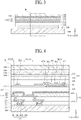
- FIG. 3 is a cross-sectional view schematically illustrating a display apparatus with integrated touch screen according to an embodiment of the present disclosure.
- FIG. 4 is an enlarged view of a portion B illustrated in FIG. 1 .
- FIG. 5 is a plan view of an insulation layer illustrated in FIG. 4 .
- FIG. 6 is a cross-sectional view taken along line I-I' illustrated in FIG. 5 .
- the display apparatus with integrated touch screen according to the present embodiment may be configured by modifying a structure of the insulation layer illustrated in FIGS. 1 and 2 .
- FIGS. 1 and 2 Hereinafter, therefore, only an insulation layer and elements relevant thereto will be described, and overlapping descriptions of the other elements are omitted.
- an insulation layer 150 may include a base layer 151 and a non-flat surface 153.
- the base layer 151 may include a molecule-adsorbing material and is the same as the insulation layer illustrated in FIGS. 1 and 2 , and thus, its overlapping description is omitted.
- the non-flat surface 153 may be provided at an interface between the insulation layer 150 and a film adhesive member 160. That is, the non-flat surface 153 may be provided as part of a surface of the base layer 151.
- the non-flat surface 153 may be defined as a concave-convex surface or a scattering surface.
- the non-flat surface 153 may increase a surface area of the insulation layer 150 to increase an adhesive surface area of the film adhesive member 160, thereby increasing an adhesive force between the insulation layer 150 and the film adhesive member 160.
- the non-flat surface 153 may act as a scattering surface at the interface between the insulation layer 150 and the film adhesive member 160 to scatter light emitted from a light emitting device layer EDL of each of a plurality of pixels P provided on a pixel array layer 110, thereby increasing a light extraction efficiency of light extracted to the outside of a window cover 190.
- the non-flat surface 153 may include a micro lens pattern provided on a surface of the base layer 151.
- the micro lens pattern may include a plurality of concave portions 153a and a partition wall 153b.
- Each of the plurality of concave portions 153a may be concavely provided to have a cross-sectional structure having a curve shape from the surface of the base layer 151.
- Each of the plurality of concave portions 153a according to an embodiment may have a cross-sectional structure of a concave lens.
- each of the plurality of concave portions 153a may have a cross-sectional structure having a semicircular shape.
- the plurality of concave portions 153a may be arranged at certain intervals in parallel along a first direction X and may be arranged in a zigzag form along a second direction Y. That is, the plurality of concave portions 153a may be arranged in a matrix form having a certain interval, and in this case, adjacent concave portions 153a may be disposed so as to be misaligned in the second direction Y. Therefore, center portions of three adjacent concave portions 153a may form a triangular shape TS. Also, the plurality of concave portions 153a may two-dimensionally have a honeycomb structure.
- the plurality of concave portions 153a may have the same depths with respect to a front surface of a planarization layer 140, but some of the plurality of concave portions 153a may have different depths due to a process error in a patterning process.
- Floors of the plurality of concave portions 153a may be spaced apart from a front surface of the planarization layer 140 by 0.1 ⁇ m to 1 ⁇ m, for preventing a portion of the front surface of the planarization layer 140 from being directly exposed at the concave portions 153a in a patterning process of patterning the insulation layer 150. That is, a thickness t1 between the floor of each of plurality of concave portions 153a and the front surface of the planarization layer 140 may be set to 0.1 ⁇ m to 1 ⁇ m.
- the partition wall 153b may be provided to surround each of the plurality of concave portions 153a.
- the partition wall 153b may two-dimensionally have a hexagonal shape.
- the partition wall 153b may have a cutting-edge structure or a convex structure, based on an interval D1 between the plurality of concave portions 153a. For example, when the interval D1 between the plurality of concave portions 153a is the same as a diameter D2 of each of the plurality of concave portions 153a, the partition wall 153b may have the cutting-edge structure.
- the partition wall 153b may have the convex structure.
- the structure of the partition wall 153b may be determined based on the interval D1 between the plurality of concave portions 153a and the diameter D2 of each of the plurality of concave portions 153a for increasing a surface area of the insulation layer 150 and light extraction efficiency.
- the partition wall 153b may include a bottom portion 153b1, a top portion 153b2, and a side portion 153b3 which are provided based on each of the plurality of concave portions 153a.
- the partition wall 153b may have a Bell or Gaussian-curve cross-sectional structure.
- the bottom portion 153b1 may be defined as a floor of a concave portion 153a adjacent to the planarization layer 140. That is, the bottom portion 153b1 may be spaced apart from the front surface of the planarization layer 140 by 0.1 ⁇ m to 1 ⁇ m.
- a diameter (or a width) of the bottom portion 153b1 may be set based on an aspect ratio of the partition wall 153b based on a height and bottom diameter of the partition wall 153b.
- the top portion 153b2 may be spaced apart from the bottom portion 153b1 by a predetermined height.
- the top portion 153b2 may be defined as a vertex of the partition wall 153b, which may have the cutting-edge structure shown in FIG. 6 , or may have the convex structure.
- the side portion 153b3 may be provided in curve shape between the bottom portion 153b1 and the top portion 153b2.
- the side portion 153b3 may include a midpoint IP, a first curve portion between the mid-point and the bottom portion 153b1, and a second curve portion between the mid-point and the top portion 153b2.
- the side portion 153b3 may include a concave surface, as shown in FIG. 6 , and both the first curve portion and the second curve portion may be concave.
- the side portion 153b3 may include both a concave surface and a convex surface.
- the first curve portion between the mid-point IP and the bottom portion 153b1 may be the concave surface
- the second curve portion between the mid-point IP and the top portion 153b2 may be the convex surface.
- the mid-point IP is an inflection point. Therefore, a traveling path of light incident on the side portion 153b3 including the inflection point may be changed at various angles by each of the concave surface and the convex surface, thereby enhancing a light extraction efficiency of each pixel.
- the insulation layer 150 may be coupled to a functional film 170 by the film adhesive member 160.
- the film adhesive member 160 may be attached on a non-flat surface (or a scattering surface) 153 provided on the insulation layer 150, and thus, an adhesive area of the film adhesive member 160 may increase, thereby increasing an adhesive force between the film adhesive member 160 and the insulation layer 150.
- the display apparatus with integrated touch screen according to the present embodiment has the same effect as that of the display apparatus illustrated in FIGS. 1 and 2 . Also, in the display apparatus with integrated touch screen according to the present embodiment, an adhesive force between the film adhesive member 160 and the insulation layer 150 increases by using the non-flat surface 153 provided on the insulation layer 150, thereby enhancing a light extraction efficiency of each pixel.
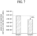
- FIG. 7 is a graph showing a result obtained by measuring an outgas fume characteristic of a single organic layer according to an embodiment of the present disclosure and an outgas fume characteristic of a single organic layer of a comparative example.
- the outgas fume characteristics have been obtained by measuring the amount of emitted outgas fume per unit area while the cured single organic layers are being reheated at a temperature of 2,300 degrees C.
- an insulation layer including an organic material with a molecule-adsorbing material added thereto may be disposed between a planarization layer and a film adhesive member, and thus, an adhesive force of a film adhesive member is prevented from being reduced by an outgas fume which is emitted from the planarization layer by heat.
- the display apparatus with integrated touch screen may be applied to televisions (TVs), wall paper TVs, monitors, notebook computers, smartphones, tablet computers, electronic pads, wearable devices, foldable devices, rollable devices, bendable devices, flexible devices, curved devices, watch phones, portable information devices, navigation devices, vehicle control display apparatuses, etc.
- TVs televisions
- wall paper TVs monitors
- notebook computers smartphones
- tablet computers electronic pads
- wearable devices foldable devices
- rollable devices rollable devices
- bendable devices flexible devices
- curved devices watch phones
- portable information devices navigation devices
- vehicle control display apparatuses etc.
Landscapes
- Engineering & Computer Science (AREA)
- Theoretical Computer Science (AREA)
- General Engineering & Computer Science (AREA)
- Physics & Mathematics (AREA)
- General Physics & Mathematics (AREA)
- Human Computer Interaction (AREA)
- Optics & Photonics (AREA)
- Computer Hardware Design (AREA)
- Spectroscopy & Molecular Physics (AREA)
- Microelectronics & Electronic Packaging (AREA)
- Quality & Reliability (AREA)
- Electroluminescent Light Sources (AREA)
- Devices For Indicating Variable Information By Combining Individual Elements (AREA)
Abstract
Description
- This application claims the benefit of the Korean Patent Application No.
10-2017-0142434 filed on October 30, 2017 - The present disclosure relates to a display apparatus with integrated touch screen.
- Touch screens are a type of input device which is installed in a display screen of an electronic device (or an information device) and enables a user to input information by touching the display screen with a finger, a pen, or the like while looking at the display screen.
- Recently, electronic devices include a display apparatus with integrated touch screen, which includes a touch screen for sensing a user touch. Particularly, display apparatuses including an organic light emitting display panel include an in-cell touch screen where a separate touch screen is not attached on the organic light emitting display panel, and a touch electrode layer including a touch electrode and a touch line is provided on an encapsulation layer of the organic light emitting display panel. An in-cell display apparatus with integrated touch screen includes a functional film (for example, a polarizing film) attached on a planarization layer which planarizes a front surface of the touch electrode layer.
- However, in the in-cell display apparatus with integrated touch screen, an adhesive force of an adhesive layer which attaches the functional film on the touch electrode layer is reduced by water, and a crack occurs in the adhesive layer due to bending of the functional film caused by a high thermal expansion coefficient of the functional film, causing a reduction in reliability.
- The above-described background is possessed by the inventor of the application for deriving the disclosure, or is technology information that has been acquired in deriving the disclosure. The above-described background is not necessarily known technology disclosed to the general public before the application of the disclosure.
- An invention is set out in the claims. Accordingly, the present disclosure is directed to provide a display apparatus with integrated touch screen that substantially obviates one or more problems due to limitations and disadvantages of the related art.
- An aspect of the present disclosure is directed to provide a display apparatus with integrated touch screen, which is improved in reliability.
- Additional advantages and features of the disclosure will be set forth in part in the description which follows and in part will become apparent to those having ordinary skill in the art upon examination of the following or may be learned from practice of the disclosure. The objectives and other advantages of the disclosure may be realized and attained by the structure particularly pointed out in the written description and claims hereof as well as the appended drawings.
- To achieve these and other advantages and in accordance with the purpose of the disclosure, as embodied and broadly described herein, there is provided a display apparatus with integrated touch screen, the display apparatus including a pixel array layer provided on a substrate, an encapsulation layer surrounding the pixel array layer, a touch electrode layer provided on the encapsulation layer, a planarization layer provided on the touch electrode layer, an insulation layer provided on the planarization layer, and a functional film attached on the insulation layer by a film adhesive member.
- It is to be understood that both the foregoing general description and the following detailed description of the present disclosure are exemplary and explanatory and are intended to provide further explanation of the disclosure as claimed.
- The accompanying drawings, which are included to provide a further understanding of the disclosure and are incorporated in and constitute a part of this application, illustrate embodiments of the disclosure and together with the description serve to explain the principle of the disclosure. In the drawings:
-
FIG. 1 is a cross-sectional view schematically illustrating a display apparatus with integrated touch screen according to an embodiment of the present disclosure; -
FIG. 2 is an enlarged view of a portion A illustrated inFIG. 1 ; -
FIG. 3 is a cross-sectional view schematically illustrating a display apparatus with integrated touch screen according to an embodiment of the present disclosure; -
FIG. 4 is an enlarged view of a portion B illustrated inFIG. 1 ; -
FIG. 5 is a plan view of an insulation layer illustrated inFIG. 4 ; -
FIG. 6 is a cross-sectional view taken along line I-I' illustrated inFIG. 5 ; and -
FIG. 7 is a graph showing a result obtained by measuring an outgas fume characteristic of a single organic layer according to an embodiment of the present disclosure and an outgas fume characteristic of a single organic layer of a comparative example. - Reference will now be made in detail to the exemplary embodiments of the present disclosure, examples of which are illustrated in the accompanying drawings. Wherever possible, the same reference numbers will be used throughout the drawings to refer to the same or like parts.
- Advantages and features of the present disclosure, and implementation methods thereof will be clarified through following embodiments described with reference to the accompanying drawings. The present disclosure may, however, be embodied in different forms and should not be construed as limited to the embodiments set forth herein. Rather, these embodiments are provided so that this disclosure will be thorough and complete, and will fully convey the scope of the present disclosure to those skilled in the art. Further, the present disclosure is only defined by scopes of claims.
- A shape, a size, a ratio, an angle, and a number disclosed in the drawings for describing embodiments of the present disclosure are merely an example, and thus, the present disclosure is not limited to the illustrated details. Like reference numerals refer to like elements throughout. In the following description, when the detailed description of the relevant known function or configuration is determined to unnecessarily obscure the important point of the present disclosure, the detailed description will be omitted.
- In a case where 'comprise', 'have', and 'include' described in the present specification are used, another part may be added unless 'only∼' is used. The terms of a singular form may include plural forms unless referred to the contrary.
- In construing an element, the element is construed as including an error range although there is no explicit description.
- In describing a position relationship, for example, when a position relation between two parts is described as 'on∼', 'over∼', 'under∼', and 'next∼', one or more other parts may be disposed between the two parts unless 'just' or 'direct' is used.
- In describing a time relationship, for example, when the temporal order is described as 'after∼', 'subsequent∼', 'next∼', and 'before∼', a case which is not continuous may be included unless 'just' or 'direct' is used.
- It will be understood that, although the terms "first", "second", etc. may be used herein to describe various elements, these elements should not be limited by these terms. These terms are only used to distinguish one element from another. For example, a first element could be termed a second element, and, similarly, a second element could be termed a first element, without departing from the scope of the present disclosure.
- The term "at least one" should be understood as including any and all combinations of one or more of the associated listed items. For example, the meaning of "at least one of a first item, a second item, and a third item" denotes the combination of all items proposed from two or more of the first item, the second item, and the third item as well as the first item, the second item, or the third item.
- Hereinafter, exemplary embodiments of a display apparatus with integrated touch screen according to the present disclosure will be described in detail with reference to the accompanying drawings. In the specification, in adding reference numerals for elements in each drawing, it should be noted that like reference numerals already used to denote like elements in other drawings are used for elements wherever possible.
-
FIG. 1 is a cross-sectional view schematically illustrating a display apparatus with integrated touch screen according to an embodiment of the present disclosure, andFIG. 2 is an enlarged view of a portion A illustrated inFIG. 1 . - Referring to
FIGS. 1 and 2 , the display apparatus with integrated touch screen according to an embodiment of the present disclosure may include asubstrate 100, apixel array layer 110, anencapsulation layer 120, atouch electrode layer 130, aplanarization layer 140, aninsulation layer 150, a filmadhesive member 160, and afunctional film 170. - The
substrate 100 may be a base substrate, and for example, may include a plastic material or a glass material. When thesubstrate 100 includes the plastic material, thesubstrate 100 may include an opaque or colored polyimide material. For example, thesubstrate 100 including a polyimide material may be formed by curing a polyimide resin which is coated to have a certain thickness on a front surface of a release layer provided on a carrier glass substrate which is relatively thick. The carrier glass substrate may be separated from thesubstrate 100 by releasing the release layer through a laser release process. - Additionally, when the
first substrate 110 includes a plastic material, the display apparatus according to the present embodiment may further include a back plate coupled to a rear surface of the substrate 100 (the rear surface of thesubstrate 100 being a surface on an opposite side of thesubstrate 100 to a surface of thesubstrate 100 facing the first substrate 110) with respect to a thickness direction (a Z-axis direction) of thesubstrate 100. The back plate may maintain thesubstrate 100 in a planar state. The back plate according to an embodiment may include a plastic material, and for example, may include polyethylene terephthalate. The back plate may be laminated on the rear surface of thesubstrate 100 separated from the carrier glass substrate. - A buffer layer may be provided on one surface of the
substrate 100. The buffer layer may be provided on the one surface of thesubstrate 100, for preventing water from penetrating into thepixel array layer 110 via thesubstrate 100 which is vulnerable to penetration of water. The buffer layer according to an embodiment may be formed of a plurality of inorganic layers which are alternately stacked. For example, the buffer layer may be formed of a multilayer where one or more inorganic layers of silicon oxide (SiOx), silicon nitride (SiNx), and silicon oxynitride (SiON) are alternately stacked. The buffer layer may be omitted. - The
pixel array layer 110 may include a thin film transistor (TFT) layer TFTL and a light emitting device layer EDL. - The TFT layer TFTL may include a plurality of
TFTs 111, agate insulation layer 112, aninterlayer insulation layer 113, apassivation layer 114, and anovercoat layer 115. Here, theTFTs 111 illustrated inFIG. 2 may each be a driving TFT connected to the light emitting device layer EDL. - The
TFTs 111 may each include an active layer ACL, a gate electrode GE, a source electrode SE, and a drain electrode DE which are provided on thesubstrate 100 or the buffer layer. InFIG. 2 , each of theTFTs 111 is illustrated as being formed in a top gate structure where the gate electrode GE is disposed on the active layer ACL, but is not limited thereto. In other embodiments, each of theTFTs 111 may be formed in a bottom gate structure where the gate electrode GE is disposed under the active layer ACL or a double gate structure where the gate electrode GE is disposed both on and under the active layer ACL. - The active layer ACL may be provided on the
substrate 100 or the buffer layer. The active layer ACL may be formed of a silicon-based semiconductor material, an oxide-based semiconductor material, and/or the like. A light blocking layer for blocking external light incident on the active layer ACL may be provided between the buffer layer and the active layer ACL. - The
gate insulation layer 112 may be provided to cover the active layer ACL. Thegate insulation layer 112 may be formed of an inorganic layer, and for example, may be formed of SiOx, SiNx, or a multilayer thereof. - The gate electrode GE may be provided on the
gate insulation layer 112 to overlap the active layer ACL. The gate electrode GE may protrude from a scan line provided on thegate insulation layer 112 to overlap the active layer ACL. The gate electrode GE and the scan line may each be formed of a single layer or a multilayer which includes one of molybdenum (Mo), aluminum (Al), chromium (Cr), gold (Au), titanium (Ti), nickel (Ni), neodymium (Nd), and copper (Cu), or an alloy thereof. - The
interlayer insulation layer 113 may be provided on the gate electrode GE and the scan line. Theinterlayer insulation layer 113 may be formed of an inorganic layer, and for example, may be formed of SiOx, SiNx, or a multilayer thereof. - The source electrode SE and the drain electrode DE may be provided on the
interlayer insulation layer 113 to overlap the active layer ACL with the gate electrode GE therebetween. In addition to the source electrode SE and the drain electrode DE, a data line may be provided on theinterlayer insulation layer 113. Each of the source electrode SE and the drain electrode DE may be connected to the active layer ACL through a contact hole which passes through thegate insulation layer 112 and theinterlayer insulation layer 113. The source electrode SE, the drain electrode DE, and the data line may each be formed of a single layer or a multilayer which includes one of Mo, Al, Cr, Au, Ti, Ni, Nd, and Cu, or an alloy thereof. - The
passivation layer 114 may be provided to cover the source electrode SE, the drain electrode DE, and the data line. Thepassivation layer 114 may insulate theTFTs 111. Thepassivation layer 114 may be formed of an inorganic layer, and for example, may be formed of SiOx, SiNx, or a multilayer thereof. - The
overcoat layer 115 may be provided to cover thepassivation layer 114. Theovercoat layer 115 may planarize a step height of an upper surface of thepassivation layer 114 caused by each of theTFTs 111. Theovercoat layer 115 may be formed of an organic layer such as acryl resin, epoxy resin, phenolic resin, polyamide resin, polyimide resin, or the like. - The light emitting device layer EDL may be provided on the TFT layer TFTL. The light emitting device layer EDL may include a
light emitting device 116 and abank 117. - The
light emitting device 116 and thebank 117 may be provided on theovercoat layer 115. - The
light emitting device 116 according to an embodiment may emit light by a light emitting layer EL emitting light based on a data signal supplied from the drivingTFT 111 of the TFT layer TFTL. Thelight emitting device 116 may include a first electrode E1, a light emitting layer EL, and a second electrode E2. The first electrode E1 may be defined as an anode electrode, and the second electrode E2 may be defined as a cathode electrode. - The first electrode E1 may be formed on the
overcoat layer 115. The first electrode E1 may be connected to the source electrode SE of the drivingTFT 111 through a contact hole which passes through thepassivation layer 114 and theovercoat layer 115. The first electrode E1 may include a metal material, which is high in reflectivity. For example, the first electrode E1 may be formed in a multilayer structure such as a stacked structure (Ti/Al/Ti) of Al and Ti, a stacked structure (ITO/Al/ITO) of Al and ITO, an APC (Ag/Pd/Cu) alloy, or a stacked structure (ITO/APC/ITO) of an APC alloy and ITO, or may include a single-layer structure including one material or two or more alloy materials selected from among Ag, Al, Mo, Au, Mg, calcium (Ca), and barium (Ba). - The
bank 117 may be provided on theovercoat layer 115 to cover an edge of the first electrode E1 and may provide an opening area OA(P) on the first electrode E1. Thebank 117 may be disposed between first electrodes E1 of adjacent pixels P and may act as a pixel defining layer which defines an opening area OA(P) of each of a plurality of pixels P. - The light emitting layer EL may be provided to cover the first electrode E1 and the
bank 117 and may be a common layer which is provided in common in the plurality of pixels P. The light emitting layer EL may include one of an organic light emitting layer, an inorganic light emitting layer, and a quantum dot light emitting layer, or may include a stacked or mixed structure of an organic light emitting layer or an inorganic light emitting layer and a quantum dot light emitting layer. - The light emitting layer EL according to an embodiment may include two or more light emitting parts for emitting white light. For example, the light emitting layer EL may include a first light emitting part and a second light emitting part for emitting the white light based on a combination of first light and second light. Here, the first light emitting part may emit the first light and may include one of a blue light emitting part, a green light emitting part, a red light emitting part, a yellow light emitting part, and a yellow-green light emitting part. The second light emitting part may include a light emitting part emitting light having a complementary color relationship among a blue light emitting part, a green light emitting part, a red light emitting part, a yellow light emitting part, and a yellow-green emitting part.
- The second electrode E2 may be provided on the light emitting layer EL. The second electrode E2 may be provided to cover the light emitting layer EL. The second electrode E2 may be a common layer which is provided in common in the pixels P. The second electrode E2 according to an embodiment may be formed of a transparent conductive material capable of transmitting light, and for example, may be formed of metal oxide, such as indium tin oxide (ITO) or indium zinc oxide (IZO), or a composition of oxide and metal such as ZnO:Al or SnO2:Sb.
- The plurality of pixels P may be provided in an area where the light emitting device layer EDL is provided, and thus, the area where the light emitting device layer EDL is provided may be defined as a display area. An area around the display area may be defined as a non-display area. The light emitting device layer EDL may emit light according to a data signal supplied through the first electrode E1 from the driving
TFT 111 of the TFT layer TFTL. At this time, light emitted from the light emitting device layer EDL may be transmitted towards thefunctional film 170. - The plurality of pixels P according to an embodiment may be arranged in a stripe structure in the display area. In this case, each of the plurality of pixels P may include a red subpixel, a green subpixel, and a blue subpixel, and moreover, may further include a white subpixel.
- According to another embodiment, the plurality of pixels P may be arranged in a pentile structure in the display area. In this case, each of the plurality of pixels P may include one red subpixel, two green subpixels, and one blue subpixel, which are one-dimensionally arranged in a polygonal form. For example, each of the pixels P having the pentile structure may include one red subpixel, two green subpixels, and one blue subpixel, which are one-dimensionally arranged in an octagonal form. In this case, the blue subpixel may have a largest size, and each of the two green subpixels may have a smallest size.
- Additionally, the display apparatus with integrated touch screen according to an embodiment of the present disclosure may further include a scan driving circuit provided in a non-display area of the
substrate 100. The scan driving circuit may generate a scan pulse according to a scan control signal and may supply the scan pulse to a corresponding scan line in a predetermined order. The scan driving circuit according to an embodiment may be provided in the non-display area of thesubstrate 100 along with the TFTs. - The
encapsulation layer 120 may be provided to surround thepixel array layer 110. The surrounding of thepixel array layer 110 by theencapsulation layer 120 may be such that thepixel array layer 110 is completely surrounded, as shown inFIG. 1 for example, by having one surface of thepixel array layer 110 covered by thesubstrate 100 and all other surfaces of thepixel array layer 110 covered by theencapsulation layer 120. Theencapsulation layer 120 protects the light emitting device layer EDL and the like from an external impact and prevents oxygen, water, and/or particles from penetrating into the light emitting layer EL and the second electrode E2 of the light emitting device layer EDL. Theencapsulation layer 120 may include at least one inorganic layer. - The
encapsulation layer 120 according to an embodiment may include a first inorganic encapsulation layer, an organic encapsulation layer, and a second inorganic encapsulation layer. - The first inorganic encapsulation layer may be provided on the
substrate 100 to surround thepixel array layer 110. The first inorganic encapsulation layer according to an embodiment may include one inorganic material of SiOx, SiNx, SiON, titanium oxide (TiOx), and aluminum oxide (AlOx). - The organic encapsulation layer may be provided on the
substrate 100 to cover the first inorganic encapsulation layer. The organic encapsulation layer may have a thickness which is relatively thicker than the first inorganic encapsulation layer, for preventing particles from penetrating into the light emitting device layer EDL via theencapsulation layer 120. The organic encapsulation layer may be formed of one organic material of acryl resin, epoxy resin, phenolic resin, polyamide resin, polyimide resin, and benzocyclobutene resin. For example, the organic encapsulation layer may be formed of epoxy resin. - The second inorganic encapsulation layer may be provided on the
substrate 100 to cover the organic encapsulation layer. The second inorganic encapsulation layer according to an embodiment may be formed of the same inorganic material as that of the first inorganic encapsulation layer. - The
touch electrode layer 130 may be provided on theencapsulation layer 120. Thetouch electrode layer 130 according to an embodiment may include a plurality of bridge electrodes BE, atouch insulation layer 131, a plurality of first touch electrodes TE1, and a plurality of second touch electrodes TE2. Thetouch electrode layer 130 may optionally also further comprise a touch buffer layer on theencapsulation layer 120. - The bridge electrodes BE may be provided on the
encapsulation layer 120. That is, the bridge electrodes BE may be respectively provided in a plurality of bridge electrode areas which are defined on the encapsulation layer. The bridge electrodes BE may have a single-layer structure or a multilayer structure including a metal material. For example, the bridge electrodes BE may have a single-layer structure or a multilayer structure including a metal material such as Mo, Ag, Ti, Cu, Al, Ti/Al/Ti, or Mo/Al/Mo. The bridge electrodes BE may be disposed to overlap thebank 117 so as to prevent the opening area OA of each pixel P from being reduced. - The
touch insulation layer 131 may be provided on theencapsulation layer 120 or the touch buffer layer to surround the bridge electrodes BE. A bridge contact hole BCH may be provided in thetouch insulation layer 131 overlapping both edges of each of the bridge electrodes BE. Thetouch insulation layer 131 according to an embodiment may be formed of an inorganic layer, and for example, may be formed of SiOx, SiNx, or a multilayer thereof. - The first touch electrodes TE1 may be provided on the
touch insulation layer 131 overlapping each of a plurality of first touch electrode areas defined on theencapsulation layer 120. Here, the first touch electrode areas may be spaced apart from one another in a first direction X. The first direction may be a direction parallel to the scan line or the data line provided on thepixel array layer 110. - The second touch electrodes TE2 may be provided on the
touch insulation layer 131 overlapping each of a plurality of second touch electrode areas defined on theencapsulation layer 120. Here, the second touch electrode areas may be spaced apart from one another in a second direction Y intersecting the first direction X. - The first and second touch electrodes TE1 and TE2 may be disposed on the same layer. The first and second touch electrodes TE1 and TE2 may be spaced apart from one another with a sensing area therebetween and may be electrically insulated from one another. The second touch electrodes TE2 spaced apart from one another in the second direction Y may be electrically connected to the bridge electrode BE through the bridge contact hole BCH provided in the
touch insulation layer 131. Therefore, the second touch electrodes TE2 spaced apart from one another in the second direction Y may be electrically connected to one another through the bridge electrode BE, and thus, the first and second touch electrodes TE1 and TE2 may be insulated from one another without being short-circuited, in an intersection area of the first and second touch electrodes TE1 and TE2. - The first and second touch electrodes TE1 and TE2, and the bridge electrodes, according to an embodiment may each include a mesh pattern where a plurality of metal lines each having a very thin line width intersect one another. The mesh pattern according to an embodiment may have a single-layer structure or a multilayer structure including a metal material such as Mo, Ag, Ti, Cu, Al, Ti/Al/Ti, or Mo/Al/Mo. The mesh pattern may be disposed to overlap the
bank 117 so as to prevent the opening area OA of each pixel P from being reduced. The first touch electrodes TE1 and the second touch electrodes TE2 may each have a mesh pattern structure and may each have a polygonal shape (for example, a lozenged or rhombic shape). In this case, the first touch electrodes TE1 and the second touch electrodes TE2 arranged in a corner of thetouch electrode layer 130 may each have a triangular shape. The mesh pattern may comprise a plurality of mesh openings or holes corresponding to the opening area OA of each pixel. - According to another embodiment, the first touch electrodes TE1 and the second touch electrodes TE2 may each have a line shape or a polygonal shape (for example, a lozenged or rhombic shape).
- The
planarization layer 140 may be provided on thesubstrate 100 to cover thetouch electrode layer 130 and may provide a flat surface on thetouch electrode layer 130. Theplanarization layer 140 according to an embodiment may be provided to have a relatively thick thickness, so as to cover the first and second touch electrodes TE1 and TE2 and thetouch insulation layer 131, and thus, may planarize a step height caused by each of the electrodes of thetouch electrode layer 130. Theplanarization layer 140 according to an embodiment may be formed of one organic material of polyacrylates resin, epoxy resin, phenolic resin, polyamide resin, polyimide resin, and benzocyclobutene resin. For example, theplanarization layer 140 may include polyacrylates resin. Theplanarization layer 140 may be formed through a coating process of coating the polyacrylates resin on thetouch electrode layer 130 and a curing process of curing the coated polyacrylates resin at a temperature of 100 degrees C or less. - The
insulation layer 150 may include a molecule-adsorbing material and may be provided on theplanarization layer 140. Theinsulation layer 150 may adsorb water to prevent the water from penetrating into thefunctional film 170, thereby reinforcing a moisture resistance of the display apparatus with integrated touch screen. Also, theinsulation layer 150 may additionally adsorb an outgas fume of theplanarization layer 140 to prevent the outgas fume from penetrating into thefunctional film 170. To this end, theinsulation layer 150 according to an embodiment of the present disclosure may include an organic material including a molecule-adsorbing material. The molecule-adsorbing material included in (added to) the organic material may be set by 5% of the volume of theinsulation layer 150 or less. In other words, the molecule-adsorbing material makes up 5% of the total volume of theinsulation layer 150. Here, when the molecule-adsorbing material included in the organic material exceeds 5%, theinsulation layer 150 may expand based on the amount of water and/or outgas fume adsorbed by the molecule-adsorbing material, causing a reduction in reliability. - The organic material of the
insulation layer 150 may include an acrylate-based material or a siloxane-based material. - The molecule-adsorbing material according to an embodiment may include a fluorine-based composition. For example, the molecule-adsorbing material including the fluorine-based composition may include Du Pont company's trademark (Nafion) molecular sieves. Here, the Nafion molecular sieves may be materials produced by hydrolyzing a perfluorosulfonic acid and may have a molecular structure represented by the following Chemical Formula 1. In the Nafion molecular sieves which are fluorine-based compositions, an end group "SO3-" may react with water molecules to adsorb polar water molecules. Also, the Nafion molecular sieves may additionally adsorb a polar outgas fume (for example, an acid composition) of the
planarization layer 140, based on heat.
- The
insulation layer 150 according to an embodiment may be formed on theplanarization layer 140 to have a thickness of 2 µm to 3 µm through the same coating process and curing process as a process of forming theplanarization layer 140. - The film
adhesive member 160 may be disposed between theinsulation layer 150 and thefunctional film 170 and may couple thefunctional film 170 to theinsulation layer 150. That is, the filmadhesive member 160 may be for laminating thefunctional film 170 on a front surface of theinsulation layer 150 and may include a pressure sensitive adhesive, an optically clear adhesive, or an optically clear resin. - The
functional film 170 may be attached on the front surface of theinsulation layer 150 by the filmadhesive member 160. Thefunctional film 170 according to an embodiment may include a polarizing film. The polarizing film may circularly polarizes external light reflected by the TFTs and/or pixel driving lines provided on thepixel array layer 110, thereby enhancing the visibility and contrast ratio of the display apparatus. According to another embodiment, thefunctional film 170 may include at least one of a polarizing film, a barrier film, an anti-reflection film, and a transmittance controllable film. - The display apparatus with integrated touch screen according to an embodiment of the present disclosure may further include a
window cover 190. - The
window cover 190 may be attached on a front surface of thefunctional film 170 by a coveradhesive member 180. Thewindow cover 190 according to an embodiment may include a plastic material, a metal material, or a glass material. In this case, the window cover 119 including the glass material may include one of sapphire glass and gorilla glass or a junction structure thereof. For example, thewindow cover 190 may include the gorilla glass which is relatively high in durability. - The cover
adhesive member 180 may be for laminating thewindow cover 190 on a front surface of thefunctional film 170 and may include a pressure sensitive adhesive, an optically clear adhesive, or an optically clear resin. - The display apparatus with integrated touch screen according to an embodiment of the present disclosure may further include a black matrix and a wavelength conversion layer which are provided on the
touch electrode layer 130. - The black matrix may define an opening area OA of each pixel P and may be provided on the
planarization layer 140 to overlap thebank 117. - The wavelength conversion layer may be provided in the opening area OA, defined by the black matrix, on the
planarization layer 140. - The wavelength conversion layer according to an embodiment may include a color filter which transmits only a wavelength of a color, set in a pixel, of white light incident from the
light emitting device 116 of each pixel P. For example, the wavelength conversion layer may transmit only a wavelength of red, green, or blue. - According to another embodiment, the wavelength conversion layer may include a quantum dot having a size which re-emits light based on the white light incident from the
light emitting device 116 of each pixel P to emit light of a color set in a pixel. Here, the quantum dot may be selected from among CdS, CdSe, CdTe, ZnS, ZnSe, GaAs, GaP, GaAs-P, Ga-Sb, InAs, InP, InSb, AlAs, AlP, and AlSb. For example, a quantum dot including CdSe or InP may emit red light, a quantum dot including CdZnSeS may emit green light, and a quantum dot including ZnSe may emit blue light. In this manner, when the wavelength conversion layer includes the quantum dot, a color reproduction rate increases. - According to another embodiment, the wavelength conversion layer may include a color filter including a quantum dot.
- In the present embodiment where the wavelength conversion layer is provided, the light emitting device layer EDL may be provided in common in each pixel P, and thus, a manufacturing process is simplified.
- In the display apparatus with integrated touch screen according to an embodiment of the present disclosure, the light emitting layer EL of the
light emitting device 116 provided as part of the light emitting device layer EDL may be divided into a red light emitting layer, a green light emitting layer, and a blue light emitting layer. In this case, the red light emitting layer, the green light emitting layer, and the blue light emitting layer may not be provided in common in each pixel P and may be individually provided in a pixel having a corresponding color. Accordingly, the black matrix and the wavelength conversion layer may be omitted. - In the display apparatus with integrated touch screen according to an embodiment of the present disclosure, water flowing in from the outside and the outgas fume emitted from the
planarization layer 140 may be adsorbed by the molecule-adsorbing material added to theinsulation layer 150, and thus, the adhesive force of the filmadhesive member 160 is prevented from being reduced by the water and the outgas fume, thereby maintaining the adhesive force of the filmadhesive member 160. Also, since the adhesive force of the filmadhesive member 160 is maintained, a crack is prevented from occurring when thefunctional film 170 is bent and the adhesive force of the filmadhesive member 160 is reduced due to heat, thereby enhancing a moisture resistance and reliability. -
FIG. 3 is a cross-sectional view schematically illustrating a display apparatus with integrated touch screen according to an embodiment of the present disclosure.FIG. 4 is an enlarged view of a portion B illustrated inFIG. 1 .FIG. 5 is a plan view of an insulation layer illustrated inFIG. 4 .FIG. 6 is a cross-sectional view taken along line I-I' illustrated inFIG. 5 . The display apparatus with integrated touch screen according to the present embodiment may be configured by modifying a structure of the insulation layer illustrated inFIGS. 1 and 2 . Hereinafter, therefore, only an insulation layer and elements relevant thereto will be described, and overlapping descriptions of the other elements are omitted. - Referring to
FIGS. 3 to 6 , aninsulation layer 150 according to the present embodiment may include abase layer 151 and anon-flat surface 153. - The
base layer 151 may include a molecule-adsorbing material and is the same as the insulation layer illustrated inFIGS. 1 and 2 , and thus, its overlapping description is omitted. - The
non-flat surface 153 may be provided at an interface between theinsulation layer 150 and a filmadhesive member 160. That is, thenon-flat surface 153 may be provided as part of a surface of thebase layer 151. Thenon-flat surface 153 may be defined as a concave-convex surface or a scattering surface. Thenon-flat surface 153 may increase a surface area of theinsulation layer 150 to increase an adhesive surface area of the filmadhesive member 160, thereby increasing an adhesive force between theinsulation layer 150 and the filmadhesive member 160. Also, thenon-flat surface 153 may act as a scattering surface at the interface between theinsulation layer 150 and the filmadhesive member 160 to scatter light emitted from a light emitting device layer EDL of each of a plurality of pixels P provided on apixel array layer 110, thereby increasing a light extraction efficiency of light extracted to the outside of awindow cover 190. - The
non-flat surface 153 according to an embodiment may include a micro lens pattern provided on a surface of thebase layer 151. The micro lens pattern may include a plurality ofconcave portions 153a and apartition wall 153b. - Each of the plurality of
concave portions 153a may be concavely provided to have a cross-sectional structure having a curve shape from the surface of thebase layer 151. Each of the plurality ofconcave portions 153a according to an embodiment may have a cross-sectional structure of a concave lens. For example, each of the plurality ofconcave portions 153a may have a cross-sectional structure having a semicircular shape. - The plurality of
concave portions 153a may be arranged at certain intervals in parallel along a first direction X and may be arranged in a zigzag form along a second direction Y. That is, the plurality ofconcave portions 153a may be arranged in a matrix form having a certain interval, and in this case, adjacentconcave portions 153a may be disposed so as to be misaligned in the second direction Y. Therefore, center portions of three adjacentconcave portions 153a may form a triangular shape TS. Also, the plurality ofconcave portions 153a may two-dimensionally have a honeycomb structure. - The plurality of
concave portions 153a may have the same depths with respect to a front surface of aplanarization layer 140, but some of the plurality ofconcave portions 153a may have different depths due to a process error in a patterning process. Floors of the plurality ofconcave portions 153a may be spaced apart from a front surface of theplanarization layer 140 by 0.1 µm to 1 µm, for preventing a portion of the front surface of theplanarization layer 140 from being directly exposed at theconcave portions 153a in a patterning process of patterning theinsulation layer 150. That is, a thickness t1 between the floor of each of plurality ofconcave portions 153a and the front surface of theplanarization layer 140 may be set to 0.1 µm to 1 µm. - For example, when a portion of the front surface of the
planarization layer 140 is directly exposed at theconcave portion 153a, the portion of the front surface of theplanarization layer 140 directly contacts the filmadhesive member 160, and for this reason, an adhesive force of the filmadhesive member 160 is reduced by an outgas fume which is emitted from theplanarization layer 140 due to heat. - The
partition wall 153b may be provided to surround each of the plurality ofconcave portions 153a. Thepartition wall 153b may two-dimensionally have a hexagonal shape. Thepartition wall 153b may have a cutting-edge structure or a convex structure, based on an interval D1 between the plurality ofconcave portions 153a. For example, when the interval D1 between the plurality ofconcave portions 153a is the same as a diameter D2 of each of the plurality ofconcave portions 153a, thepartition wall 153b may have the cutting-edge structure. As another example, when the interval D1 between the plurality ofconcave portions 153a is greater than the diameter D2 of each of the plurality ofconcave portions 153a, thepartition wall 153b may have the convex structure. The structure of thepartition wall 153b may be determined based on the interval D1 between the plurality ofconcave portions 153a and the diameter D2 of each of the plurality ofconcave portions 153a for increasing a surface area of theinsulation layer 150 and light extraction efficiency. - The
partition wall 153b may include a bottom portion 153b1, a top portion 153b2, and a side portion 153b3 which are provided based on each of the plurality ofconcave portions 153a. In the case that thepartition wall 153b has the convex structure, thepartition wall 153b may have a Bell or Gaussian-curve cross-sectional structure. - The bottom portion 153b1 may be defined as a floor of a
concave portion 153a adjacent to theplanarization layer 140. That is, the bottom portion 153b1 may be spaced apart from the front surface of theplanarization layer 140 by 0.1 µm to 1 µm. A diameter (or a width) of the bottom portion 153b1 may be set based on an aspect ratio of thepartition wall 153b based on a height and bottom diameter of thepartition wall 153b. - The top portion 153b2 may be spaced apart from the bottom portion 153b1 by a predetermined height. The top portion 153b2 may be defined as a vertex of the
partition wall 153b, which may have the cutting-edge structure shown inFIG. 6 , or may have the convex structure. - The side portion 153b3 may be provided in curve shape between the bottom portion 153b1 and the top portion 153b2. The side portion 153b3 according to an embodiment may include a midpoint IP, a first curve portion between the mid-point and the bottom portion 153b1, and a second curve portion between the mid-point and the top portion 153b2. The side portion 153b3 may include a concave surface, as shown in
FIG. 6 , and both the first curve portion and the second curve portion may be concave. Alternatively, the side portion 153b3 may include both a concave surface and a convex surface. In this case, the first curve portion between the mid-point IP and the bottom portion 153b1 may be the concave surface, and the second curve portion between the mid-point IP and the top portion 153b2 may be the convex surface. As such, in this arrangement the mid-point IP is an inflection point. Therefore, a traveling path of light incident on the side portion 153b3 including the inflection point may be changed at various angles by each of the concave surface and the convex surface, thereby enhancing a light extraction efficiency of each pixel. - The
insulation layer 150 according to the present embodiment may be coupled to afunctional film 170 by the filmadhesive member 160. In this case, the filmadhesive member 160 may be attached on a non-flat surface (or a scattering surface) 153 provided on theinsulation layer 150, and thus, an adhesive area of the filmadhesive member 160 may increase, thereby increasing an adhesive force between the filmadhesive member 160 and theinsulation layer 150. - As described above, the display apparatus with integrated touch screen according to the present embodiment has the same effect as that of the display apparatus illustrated in
FIGS. 1 and 2 . Also, in the display apparatus with integrated touch screen according to the present embodiment, an adhesive force between the filmadhesive member 160 and theinsulation layer 150 increases by using thenon-flat surface 153 provided on theinsulation layer 150, thereby enhancing a light extraction efficiency of each pixel. -
FIG. 7 is a graph showing a result obtained by measuring an outgas fume characteristic of a single organic layer according to an embodiment of the present disclosure and an outgas fume characteristic of a single organic layer of a comparative example. InFIG. 7 , after a single organic layer (Sample 1), to which a molecule-adsorbing material is not added, of the comparative example and a single organic layer (Sample 2), to which a molecule-adsorbing material is added by 5% or less, of the present disclosure are cured, the outgas fume characteristics have been obtained by measuring the amount of emitted outgas fume per unit area while the cured single organic layers are being reheated at a temperature of 2,300 degrees C. - As seen in
FIG. 7 , in comparison with the single organic layer (Sample 1) of the comparative example, it can be confirmed that in the single organic layer (Sample 2) of the present disclosure, the amount of emitted outgas fume is reduced by about 20%. - Therefore, according to the present disclosure, an insulation layer including an organic material with a molecule-adsorbing material added thereto may be disposed between a planarization layer and a film adhesive member, and thus, an adhesive force of a film adhesive member is prevented from being reduced by an outgas fume which is emitted from the planarization layer by heat.
- The display apparatus with integrated touch screen according to the embodiments of the present disclosure may be applied to televisions (TVs), wall paper TVs, monitors, notebook computers, smartphones, tablet computers, electronic pads, wearable devices, foldable devices, rollable devices, bendable devices, flexible devices, curved devices, watch phones, portable information devices, navigation devices, vehicle control display apparatuses, etc.
- The above-described feature, structure, and effect of the present disclosure are included in at least one embodiment of the present disclosure, but are not limited to only one embodiment. Furthermore, the feature, structure, and effect described in at least one embodiment of the present disclosure may be implemented through combination or modification of other embodiments by those skilled in the art. Therefore, content associated with the combination and modification should be construed as being within the scope of the present disclosure.
- As described above, in the display apparatus with integrated touch screen, a problem where the adhesive force of the film adhesive member is reduced by the outgas fume is solved, and thus, a crack which occurs in the film adhesive member due to the reduction in the adhesive force is prevented, thereby enhancing a moisture resistance and reliability.
- It will be apparent to those skilled in the art that various modifications and variations can be made in the present disclosure without departing from the scope of the disclosures. Thus, it is intended that the present disclosure covers the modifications and variations of this disclosure provided they come within the scope of the appended claims. Also disclosed herein are the following numbered clauses:
- Clause 1. A display apparatus with integrated touch screen, the display apparatus comprising:
- a pixel array layer on a substrate;
- an encapsulation layer surrounding the pixel array layer;
- a touch electrode layer on the encapsulation layer;
- a planarization layer on the touch electrode layer;
- an insulation layer on the planarization layer; and
- a functional film attached on the insulation layer by a film adhesive member,
- wherein the insulation layer comprises a molecule-adsorbing material.
- Clause 2. The display apparatus of any preceding clause, wherein the molecule-adsorbing material comprises water molecules.
-
Clause 3. The display apparatus of any preceding clause, wherein the molecule-adsorbing material adsorbs an outgas fume of the planarization layer. -
Clause 4. The display apparatus of any preceding clause, wherein the molecule-adsorbing material comprises a fluorine-based composition. - Clause 5. The display apparatus of any preceding clause, wherein
the insulation layer comprises an organic material comprising the molecule-adsorbing material, and
the molecule-adsorbing material comprises Nafion molecular sieves. - Clause 6. The display apparatus of any preceding clause, wherein the insulation layer comprises an organic material comprising the molecule-adsorbing material, and
wherein the organic material of the insulation layer comprises an acrylate-based material or a siloxane-based material. - Clause 7. The display apparatus of any preceding clause, wherein the film adhesive member comprises a pressure sensitive adhesive, an optically clear adhesive, or an optically clear resin.
- Clause 8. The display apparatus of any preceding clause, wherein the planarization layer comprises one of polyacrylates resin, epoxy resin, phenolic resin, polyamide resin, polyimide resin, and benzocyclobutene resin.
- Clause 9. The display apparatus of any preceding clause, wherein the functional film comprises a polarizing film.
- Clause 10. The display apparatus of any preceding clause, wherein an interface between the insulation layer and the film adhesive member is a non-flat surface.
- Clause 11. The display apparatus of any preceding clause, wherein
the insulation layer comprises a scattering layer, and
the film adhesive member is attached on the scattering layer. - Clause 12. The display apparatus of any preceding clause, wherein
the insulation layer comprises:- a base layer including the molecule-adsorbing material; and
- a non-flat surface including a micro lens pattern provided on a surface of the base layer, and
- the film adhesive member is attached on the micro lens pattern.
- Clause 13. The display apparatus of any preceding clause, wherein the functional film comprises a polarizing film.
- Clause 14. The display apparatus of one of clauses 1 to 11, wherein
the insulation layer further comprises a micro lens pattern, and
the film adhesive member is attached on the micro lens pattern. - Clause 15. The display apparatus of any preceding clause, wherein the molecule-adsorbing material added to the insulation layer is set by 5% or less.
Claims (18)
- A display apparatus with integrated touch screen, the display apparatus comprising:a pixel array layer (110) on a substrate (100);an encapsulation layer (120) surrounding the pixel array layer;a touch electrode layer (130) on the encapsulation layer;an insulation layer (150) on the touch electrode layer,wherein the insulation layer (150) comprises a scattering surface including a micro lens pattern.
- The display apparatus of claim 1, further comprising a planarization layer (140) on the touch electrode layer (130), between the touch electrode layer (130) and the insulation layer (150).
- The display apparatus of claim 1 or 2, further comprising a functional film (170) attached on the insulation layer (150) by a film adhesive member (160).
- The display apparatus of any preceding claim, wherein the insulation layer (150) comprises a molecule-adsorbing material.
- The display apparatus of any preceding claim, wherein the touch electrode layer (130) comprises a plurality of bridge electrodes (BE) on the encapsulation layer (120), a touch insulation layer (131) on the bridge electrodes (BE), and a plurality of touch electrodes (TE1, TE2) on the touch insulation layer (131), and optionally wherein the touch electrode layer (130) further comprises a touch buffer layer between the touch insulation layer (131) and the encapsulation layer (120).
- The display apparatus of claim 5, wherein the plurality of touch electrodes and the plurality of bridge electrodes (BE) each comprises a mesh pattern.
- The display apparatus of any preceding claim, wherein the molecule-adsorbing material adsorbs water molecules, and optionally wherein the molecule-adsorbing material comprises a fluorine-based composition.
- The display apparatus of any preceding claim, wherein the molecule-adsorbing material adsorbs an outgas fume of the planarization layer (140).
- The display apparatus of any preceding claim, wherein
the insulation layer (150) comprises an organic material comprising the molecule-adsorbing material, and
the molecule-adsorbing material comprises Nafion molecular sieves. - The display apparatus of any preceding claim, wherein the insulation layer (150) comprises an organic material comprising the molecule-adsorbing material, and
wherein the organic material of the insulation layer comprises an acrylate-based material or a siloxane-based material. - The display apparatus of claim 3, wherein the film adhesive member (160) comprises a pressure sensitive adhesive, an optically clear adhesive, or an optically clear resin.
- The display apparatus of any preceding claim, wherein the planarization layer (140) comprises one of polyacrylates resin, epoxy resin, phenolic resin, polyamide resin, polyimide resin, and benzocyclobutene resin.
- The display apparatus of claim 3 or 11, wherein the functional film (170) comprises a polarizing film.
- The display apparatus of claim 3, 11 or 13, wherein the scattering surface (153) is a non-flat surface providing an interface between the insulation layer (150) and the film adhesive member (160).
- The display apparatus of claims 3, 11, 13 or 14, wherein
the film adhesive member (160) is attached on the scattering surface. - The display apparatus of any preceding claim, wherein
the insulation layer (150) comprises:a base layer (151) including the molecule-adsorbing material; andthe scattering surface (153),wherein the film adhesive member (160) is attached to the micro lens pattern of the scattering surface. - The display apparatus of any preceding claim, wherein the micro lens pattern comprises:a plurality of concave portions (153a) and at least one partition wall (153b), the at least one partition wall being disposed between adjacent concave portions of the plurality of concave portions.
- The display apparatus of any preceding claim, wherein the molecule-adsorbing material added to the insulation layer (150) is 5% or less of a total volume of the insulation layer (150).
Applications Claiming Priority (1)
| Application Number | Priority Date | Filing Date | Title |
|---|---|---|---|
| KR1020170142434A KR102373995B1 (en) | 2017-10-30 | 2017-10-30 | Display apparatus with integrated touch screen |
Publications (2)
| Publication Number | Publication Date |
|---|---|
| EP3477446A1 true EP3477446A1 (en) | 2019-05-01 |
| EP3477446B1 EP3477446B1 (en) | 2020-04-29 |
Family
ID=64051463
Family Applications (1)
| Application Number | Title | Priority Date | Filing Date |
|---|---|---|---|
| EP18202977.7A Active EP3477446B1 (en) | 2017-10-30 | 2018-10-26 | Display apparatus with integrated touch screen |
Country Status (5)
| Country | Link |
|---|---|
| US (1) | US11199918B2 (en) |
| EP (1) | EP3477446B1 (en) |
| JP (1) | JP6791930B2 (en) |
| KR (1) | KR102373995B1 (en) |
| CN (1) | CN109725763B (en) |
Cited By (1)
| Publication number | Priority date | Publication date | Assignee | Title |
|---|---|---|---|---|
| US20230217733A1 (en) * | 2021-12-30 | 2023-07-06 | Lg Display Co., Ltd. | Display device |
Families Citing this family (15)
| Publication number | Priority date | Publication date | Assignee | Title |
|---|---|---|---|---|
| KR102747339B1 (en) * | 2019-02-19 | 2025-01-02 | 삼성디스플레이 주식회사 | Display device |
| KR102830387B1 (en) * | 2019-04-23 | 2025-07-07 | 삼성디스플레이 주식회사 | Display apparatus |
| KR102734911B1 (en) * | 2019-05-08 | 2024-11-26 | 엘지디스플레이 주식회사 | Display apparatus |
| CN110221730B (en) * | 2019-06-17 | 2022-06-07 | 京东方科技集团股份有限公司 | Touch panel and touch display device |
| CN112631450A (en) * | 2019-10-09 | 2021-04-09 | 群创光电股份有限公司 | Electronic device |
| KR102928330B1 (en) * | 2019-10-30 | 2026-02-19 | 삼성디스플레이 주식회사 | Manufacturing method of display device and display device manufactured using the same |
| KR102510120B1 (en) | 2019-11-06 | 2023-03-15 | 엘지디스플레이 주식회사 | Touch display device |
| KR102724697B1 (en) * | 2020-02-21 | 2024-11-01 | 삼성디스플레이 주식회사 | Display apparatus and flexible display apparatus |
| CN111430565B (en) * | 2020-03-30 | 2022-07-12 | 武汉华星光电半导体显示技术有限公司 | Display device and method for manufacturing display device |
| CN111725271B (en) * | 2020-06-09 | 2022-10-04 | 武汉华星光电半导体显示技术有限公司 | OLED display panel |
| KR102344074B1 (en) * | 2020-06-11 | 2021-12-29 | (주)휴넷플러스 | Quantum Dot Organic Light Emitting Display Device with InCell Light Extraction function |
| CN114356149A (en) * | 2020-10-13 | 2022-04-15 | 群创光电股份有限公司 | Transparent touch display device |
| KR102888982B1 (en) * | 2020-11-23 | 2025-11-19 | 엘지디스플레이 주식회사 | Display device |
| CN114284320A (en) * | 2021-12-16 | 2022-04-05 | 合肥维信诺科技有限公司 | Display panel and display device |
| US12624993B2 (en) | 2022-01-19 | 2026-05-12 | AUO Corporation | Sensing device and method for fabricating the same |
Citations (6)
| Publication number | Priority date | Publication date | Assignee | Title |
|---|---|---|---|---|
| US20110128240A1 (en) * | 2009-12-01 | 2011-06-02 | Howon Choi | Display device with a touch device |
| US20140070350A1 (en) * | 2012-09-11 | 2014-03-13 | Samsung Display Co., Ltd. | Sensor substrate, method of manufacturing the same and sensing display panel having the same |
| US20160260780A1 (en) * | 2015-03-02 | 2016-09-08 | Samsung Display Co., Ltd. | Method for fabricating display device and display device |
| US20160363797A1 (en) * | 2014-02-28 | 2016-12-15 | Toppan Printing Co., Ltd. | Liquid crystal display device |
| US20170010493A1 (en) * | 2015-05-29 | 2017-01-12 | Wuhan China Star Optoelectronics Technology Co., Ltd. | Self-capacitance in-cell touch screen and method of manufacturing the same, liquid crystal display |
| US20170256593A1 (en) * | 2016-03-03 | 2017-09-07 | Samsung Display Co., Ltd. | Touch display panel and method of manufacturing the same |
Family Cites Families (17)
| Publication number | Priority date | Publication date | Assignee | Title |
|---|---|---|---|---|
| US20050238803A1 (en) * | 2003-11-12 | 2005-10-27 | Tremel James D | Method for adhering getter material to a surface for use in electronic devices |
| JP2006156075A (en) * | 2004-11-29 | 2006-06-15 | Seiko Epson Corp | Electro-optical device manufacturing method and image forming apparatus |
| ITMI20052496A1 (en) * | 2005-12-27 | 2007-06-28 | Getters Spa | COMPOSITE SYSTEMS GAS ABSORBERS AND METHODS FOR THEIR PRODUCTION |
| KR20130007006A (en) | 2011-06-28 | 2013-01-18 | 삼성디스플레이 주식회사 | Organic light emitting display device and method of manufacturing an organic light emitting display device |
| JP2013052569A (en) * | 2011-09-02 | 2013-03-21 | Konica Minolta Advanced Layers Inc | Method for manufacturing moisture vapor barrier film, moisture vapor barrier film, and electric equipment |
| KR101552994B1 (en) * | 2012-08-31 | 2015-09-15 | 엘지디스플레이 주식회사 | Organic Emitting Display Device and Method for Manufacturing the Same |
| CN203012678U (en) * | 2012-10-25 | 2013-06-19 | 上海理工大学 | Fly eye bionic touch screen |
| US9111464B2 (en) * | 2013-06-18 | 2015-08-18 | LuxVue Technology Corporation | LED display with wavelength conversion layer |
| JP2015143933A (en) | 2014-01-31 | 2015-08-06 | 株式会社ジャパンディスプレイ | Display device with capacitance sensor and driving method therefor |
| KR102289050B1 (en) * | 2014-04-16 | 2021-08-12 | 삼성디스플레이 주식회사 | Display device |
| US9676175B2 (en) * | 2014-06-20 | 2017-06-13 | Semiconductor Energy Laboratory Co., Ltd. | Peeling apparatus |
| JP6832634B2 (en) * | 2015-05-29 | 2021-02-24 | 株式会社半導体エネルギー研究所 | Semiconductor device |
| US10168844B2 (en) * | 2015-06-26 | 2019-01-01 | Samsung Display Co., Ltd. | Flexible display device |
| KR102443918B1 (en) * | 2016-01-22 | 2022-09-19 | 삼성디스플레이 주식회사 | flexible display device |
| KR20170040400A (en) * | 2015-10-02 | 2017-04-13 | 삼성디스플레이 주식회사 | Touch screen panel, method of manufacturing the same and touch display devicd having the same |
| KR102439350B1 (en) | 2015-12-31 | 2022-09-02 | 엘지디스플레이 주식회사 | Touch screen built-in display device and manufacturing method thereof |
| JP6486859B2 (en) | 2016-03-29 | 2019-03-20 | 日東電工株式会社 | Polarizing film and image display device |
-
2017
- 2017-10-30 KR KR1020170142434A patent/KR102373995B1/en active Active
-
2018
- 2018-10-26 EP EP18202977.7A patent/EP3477446B1/en active Active
- 2018-10-29 CN CN201811267964.7A patent/CN109725763B/en active Active
- 2018-10-29 US US16/173,629 patent/US11199918B2/en active Active
- 2018-10-30 JP JP2018203552A patent/JP6791930B2/en active Active
Patent Citations (6)
| Publication number | Priority date | Publication date | Assignee | Title |
|---|---|---|---|---|
| US20110128240A1 (en) * | 2009-12-01 | 2011-06-02 | Howon Choi | Display device with a touch device |
| US20140070350A1 (en) * | 2012-09-11 | 2014-03-13 | Samsung Display Co., Ltd. | Sensor substrate, method of manufacturing the same and sensing display panel having the same |
| US20160363797A1 (en) * | 2014-02-28 | 2016-12-15 | Toppan Printing Co., Ltd. | Liquid crystal display device |
| US20160260780A1 (en) * | 2015-03-02 | 2016-09-08 | Samsung Display Co., Ltd. | Method for fabricating display device and display device |
| US20170010493A1 (en) * | 2015-05-29 | 2017-01-12 | Wuhan China Star Optoelectronics Technology Co., Ltd. | Self-capacitance in-cell touch screen and method of manufacturing the same, liquid crystal display |
| US20170256593A1 (en) * | 2016-03-03 | 2017-09-07 | Samsung Display Co., Ltd. | Touch display panel and method of manufacturing the same |
Cited By (2)
| Publication number | Priority date | Publication date | Assignee | Title |
|---|---|---|---|---|
| US20230217733A1 (en) * | 2021-12-30 | 2023-07-06 | Lg Display Co., Ltd. | Display device |
| US12382791B2 (en) * | 2021-12-30 | 2025-08-05 | Lg Display Co., Ltd. | Display device including a micro lens array |
Also Published As
| Publication number | Publication date |
|---|---|
| JP6791930B2 (en) | 2020-11-25 |
| JP2019082685A (en) | 2019-05-30 |
| US20190129554A1 (en) | 2019-05-02 |
| US11199918B2 (en) | 2021-12-14 |
| CN109725763B (en) | 2022-04-05 |
| CN109725763A (en) | 2019-05-07 |
| KR20190047993A (en) | 2019-05-09 |
| EP3477446B1 (en) | 2020-04-29 |
| KR102373995B1 (en) | 2022-03-11 |
Similar Documents
| Publication | Publication Date | Title |
|---|---|---|
| EP3477446B1 (en) | Display apparatus with integrated touch screen | |
| US11526244B2 (en) | Touch screen panel and display apparatus with integrated touch screen | |
| CN111129076B (en) | Display device | |
| KR101998949B1 (en) | Display device and method of manufacturing display device | |
| US9118036B2 (en) | Organic light emitting device and method of manufacturing the same | |
| KR102746584B1 (en) | Flexible display device | |
| KR102162912B1 (en) | Organic electroluminescent device having touch panel and method for fabricating the same | |
| US10854850B2 (en) | Organic light-emitting diode display device | |
| CN112783363A (en) | Touch display device | |
| US20160124557A1 (en) | Organic light emitting display device and method for manufacturing the same | |
| CN110120401A (en) | Show equipment | |
| CN105390526A (en) | In-cell type touch panel integrated flexible organic light emitting display device | |
| KR20160015815A (en) | Organic light emitting display apparatus | |
| US9960377B2 (en) | Color filter substrate and fabrication method thereof, OLED structure, related display panel, and related display device | |
| KR20170088474A (en) | Flexible display device | |
| KR20220097681A (en) | Display device | |
| KR102658429B1 (en) | Cover Window and Flexible Display Device Using the Same | |
| CN221127823U (en) | Display device | |
| CN104183614A (en) | Organic light emitting display device | |
| KR102968285B1 (en) | Touch display device and display panel | |
| US20220197432A1 (en) | Electronic device | |
| KR20260014067A (en) | Display device | |
| KR102407526B1 (en) | Light controlling apparatus, and transparent display device using the same | |
| KR20250040777A (en) | Display device | |
| KR20210080953A (en) | Touch display device and display panel |
Legal Events
| Date | Code | Title | Description |
|---|---|---|---|
| PUAI | Public reference made under article 153(3) epc to a published international application that has entered the european phase |
Free format text: ORIGINAL CODE: 0009012 |
|
| STAA | Information on the status of an ep patent application or granted ep patent |
Free format text: STATUS: REQUEST FOR EXAMINATION WAS MADE |
|
| 17P | Request for examination filed |
Effective date: 20181026 |
|
| AK | Designated contracting states |
Kind code of ref document: A1 Designated state(s): AL AT BE BG CH CY CZ DE DK EE ES FI FR GB GR HR HU IE IS IT LI LT LU LV MC MK MT NL NO PL PT RO RS SE SI SK SM TR |
|
| AX | Request for extension of the european patent |
Extension state: BA ME |
|
| RBV | Designated contracting states (corrected) |
Designated state(s): AL AT BE BG CH CY CZ DE DK EE ES FI FR GB GR HR HU IE IS IT LI LT LU LV MC MK MT NL NO PL PT RO RS SE SI SK SM TR |
|
| GRAP | Despatch of communication of intention to grant a patent |
Free format text: ORIGINAL CODE: EPIDOSNIGR1 |
|
| STAA | Information on the status of an ep patent application or granted ep patent |
Free format text: STATUS: GRANT OF PATENT IS INTENDED |
|
| INTG | Intention to grant announced |
Effective date: 20191113 |
|
| GRAS | Grant fee paid |
Free format text: ORIGINAL CODE: EPIDOSNIGR3 |
|
| GRAA | (expected) grant |
Free format text: ORIGINAL CODE: 0009210 |
|
| STAA | Information on the status of an ep patent application or granted ep patent |
Free format text: STATUS: THE PATENT HAS BEEN GRANTED |
|
| AK | Designated contracting states |
Kind code of ref document: B1 Designated state(s): AL AT BE BG CH CY CZ DE DK EE ES FI FR GB GR HR HU IE IS IT LI LT LU LV MC MK MT NL NO PL PT RO RS SE SI SK SM TR |
|
| REG | Reference to a national code |
Ref country code: GB Ref legal event code: FG4D |
|
| REG | Reference to a national code |
Ref country code: CH Ref legal event code: EP |
|
| REG | Reference to a national code |
Ref country code: AT Ref legal event code: REF Ref document number: 1264316 Country of ref document: AT Kind code of ref document: T Effective date: 20200515 |
|
| REG | Reference to a national code |
Ref country code: DE Ref legal event code: R096 Ref document number: 602018004197 Country of ref document: DE |
|
| REG | Reference to a national code |
Ref country code: IE Ref legal event code: FG4D |
|
| REG | Reference to a national code |
Ref country code: NL Ref legal event code: MP Effective date: 20200429 |
|
| REG | Reference to a national code |
Ref country code: LT Ref legal event code: MG4D |
|
| PG25 | Lapsed in a contracting state [announced via postgrant information from national office to epo] |
Ref country code: LT Free format text: LAPSE BECAUSE OF FAILURE TO SUBMIT A TRANSLATION OF THE DESCRIPTION OR TO PAY THE FEE WITHIN THE PRESCRIBED TIME-LIMIT Effective date: 20200429 Ref country code: FI Free format text: LAPSE BECAUSE OF FAILURE TO SUBMIT A TRANSLATION OF THE DESCRIPTION OR TO PAY THE FEE WITHIN THE PRESCRIBED TIME-LIMIT Effective date: 20200429 Ref country code: SE Free format text: LAPSE BECAUSE OF FAILURE TO SUBMIT A TRANSLATION OF THE DESCRIPTION OR TO PAY THE FEE WITHIN THE PRESCRIBED TIME-LIMIT Effective date: 20200429 Ref country code: NO Free format text: LAPSE BECAUSE OF FAILURE TO SUBMIT A TRANSLATION OF THE DESCRIPTION OR TO PAY THE FEE WITHIN THE PRESCRIBED TIME-LIMIT Effective date: 20200729 Ref country code: PT Free format text: LAPSE BECAUSE OF FAILURE TO SUBMIT A TRANSLATION OF THE DESCRIPTION OR TO PAY THE FEE WITHIN THE PRESCRIBED TIME-LIMIT Effective date: 20200831 Ref country code: IS Free format text: LAPSE BECAUSE OF FAILURE TO SUBMIT A TRANSLATION OF THE DESCRIPTION OR TO PAY THE FEE WITHIN THE PRESCRIBED TIME-LIMIT Effective date: 20200829 Ref country code: GR Free format text: LAPSE BECAUSE OF FAILURE TO SUBMIT A TRANSLATION OF THE DESCRIPTION OR TO PAY THE FEE WITHIN THE PRESCRIBED TIME-LIMIT Effective date: 20200730 |
|
| REG | Reference to a national code |
Ref country code: AT Ref legal event code: MK05 Ref document number: 1264316 Country of ref document: AT Kind code of ref document: T Effective date: 20200429 |
|
| PG25 | Lapsed in a contracting state [announced via postgrant information from national office to epo] |
Ref country code: RS Free format text: LAPSE BECAUSE OF FAILURE TO SUBMIT A TRANSLATION OF THE DESCRIPTION OR TO PAY THE FEE WITHIN THE PRESCRIBED TIME-LIMIT Effective date: 20200429 Ref country code: LV Free format text: LAPSE BECAUSE OF FAILURE TO SUBMIT A TRANSLATION OF THE DESCRIPTION OR TO PAY THE FEE WITHIN THE PRESCRIBED TIME-LIMIT Effective date: 20200429 Ref country code: HR Free format text: LAPSE BECAUSE OF FAILURE TO SUBMIT A TRANSLATION OF THE DESCRIPTION OR TO PAY THE FEE WITHIN THE PRESCRIBED TIME-LIMIT Effective date: 20200429 Ref country code: BG Free format text: LAPSE BECAUSE OF FAILURE TO SUBMIT A TRANSLATION OF THE DESCRIPTION OR TO PAY THE FEE WITHIN THE PRESCRIBED TIME-LIMIT Effective date: 20200729 |
|
| PG25 | Lapsed in a contracting state [announced via postgrant information from national office to epo] |
Ref country code: NL Free format text: LAPSE BECAUSE OF FAILURE TO SUBMIT A TRANSLATION OF THE DESCRIPTION OR TO PAY THE FEE WITHIN THE PRESCRIBED TIME-LIMIT Effective date: 20200429 Ref country code: AL Free format text: LAPSE BECAUSE OF FAILURE TO SUBMIT A TRANSLATION OF THE DESCRIPTION OR TO PAY THE FEE WITHIN THE PRESCRIBED TIME-LIMIT Effective date: 20200429 |
|
| PG25 | Lapsed in a contracting state [announced via postgrant information from national office to epo] |
Ref country code: CZ Free format text: LAPSE BECAUSE OF FAILURE TO SUBMIT A TRANSLATION OF THE DESCRIPTION OR TO PAY THE FEE WITHIN THE PRESCRIBED TIME-LIMIT Effective date: 20200429 Ref country code: ES Free format text: LAPSE BECAUSE OF FAILURE TO SUBMIT A TRANSLATION OF THE DESCRIPTION OR TO PAY THE FEE WITHIN THE PRESCRIBED TIME-LIMIT Effective date: 20200429 Ref country code: EE Free format text: LAPSE BECAUSE OF FAILURE TO SUBMIT A TRANSLATION OF THE DESCRIPTION OR TO PAY THE FEE WITHIN THE PRESCRIBED TIME-LIMIT Effective date: 20200429 Ref country code: SM Free format text: LAPSE BECAUSE OF FAILURE TO SUBMIT A TRANSLATION OF THE DESCRIPTION OR TO PAY THE FEE WITHIN THE PRESCRIBED TIME-LIMIT Effective date: 20200429 Ref country code: DK Free format text: LAPSE BECAUSE OF FAILURE TO SUBMIT A TRANSLATION OF THE DESCRIPTION OR TO PAY THE FEE WITHIN THE PRESCRIBED TIME-LIMIT Effective date: 20200429 Ref country code: RO Free format text: LAPSE BECAUSE OF FAILURE TO SUBMIT A TRANSLATION OF THE DESCRIPTION OR TO PAY THE FEE WITHIN THE PRESCRIBED TIME-LIMIT Effective date: 20200429 Ref country code: IT Free format text: LAPSE BECAUSE OF FAILURE TO SUBMIT A TRANSLATION OF THE DESCRIPTION OR TO PAY THE FEE WITHIN THE PRESCRIBED TIME-LIMIT Effective date: 20200429 Ref country code: AT Free format text: LAPSE BECAUSE OF FAILURE TO SUBMIT A TRANSLATION OF THE DESCRIPTION OR TO PAY THE FEE WITHIN THE PRESCRIBED TIME-LIMIT Effective date: 20200429 |
|
| REG | Reference to a national code |
Ref country code: DE Ref legal event code: R097 Ref document number: 602018004197 Country of ref document: DE |
|
| PG25 | Lapsed in a contracting state [announced via postgrant information from national office to epo] |
Ref country code: PL Free format text: LAPSE BECAUSE OF FAILURE TO SUBMIT A TRANSLATION OF THE DESCRIPTION OR TO PAY THE FEE WITHIN THE PRESCRIBED TIME-LIMIT Effective date: 20200429 Ref country code: SK Free format text: LAPSE BECAUSE OF FAILURE TO SUBMIT A TRANSLATION OF THE DESCRIPTION OR TO PAY THE FEE WITHIN THE PRESCRIBED TIME-LIMIT Effective date: 20200429 |
|
| PLBE | No opposition filed within time limit |
Free format text: ORIGINAL CODE: 0009261 |
|
| STAA | Information on the status of an ep patent application or granted ep patent |
Free format text: STATUS: NO OPPOSITION FILED WITHIN TIME LIMIT |
|
| 26N | No opposition filed |
Effective date: 20210201 |
|
| PG25 | Lapsed in a contracting state [announced via postgrant information from national office to epo] |
Ref country code: SI Free format text: LAPSE BECAUSE OF FAILURE TO SUBMIT A TRANSLATION OF THE DESCRIPTION OR TO PAY THE FEE WITHIN THE PRESCRIBED TIME-LIMIT Effective date: 20200429 |
|
| PG25 | Lapsed in a contracting state [announced via postgrant information from national office to epo] |
Ref country code: MC Free format text: LAPSE BECAUSE OF FAILURE TO SUBMIT A TRANSLATION OF THE DESCRIPTION OR TO PAY THE FEE WITHIN THE PRESCRIBED TIME-LIMIT Effective date: 20200429 Ref country code: LU Free format text: LAPSE BECAUSE OF NON-PAYMENT OF DUE FEES Effective date: 20201026 |
|
| REG | Reference to a national code |
Ref country code: BE Ref legal event code: MM Effective date: 20201031 |
|
| PG25 | Lapsed in a contracting state [announced via postgrant information from national office to epo] |
Ref country code: BE Free format text: LAPSE BECAUSE OF NON-PAYMENT OF DUE FEES Effective date: 20201031 |
|
| PG25 | Lapsed in a contracting state [announced via postgrant information from national office to epo] |
Ref country code: IE Free format text: LAPSE BECAUSE OF NON-PAYMENT OF DUE FEES Effective date: 20201026 |
|
| PG25 | Lapsed in a contracting state [announced via postgrant information from national office to epo] |
Ref country code: TR Free format text: LAPSE BECAUSE OF FAILURE TO SUBMIT A TRANSLATION OF THE DESCRIPTION OR TO PAY THE FEE WITHIN THE PRESCRIBED TIME-LIMIT Effective date: 20200429 Ref country code: MT Free format text: LAPSE BECAUSE OF FAILURE TO SUBMIT A TRANSLATION OF THE DESCRIPTION OR TO PAY THE FEE WITHIN THE PRESCRIBED TIME-LIMIT Effective date: 20200429 Ref country code: CY Free format text: LAPSE BECAUSE OF FAILURE TO SUBMIT A TRANSLATION OF THE DESCRIPTION OR TO PAY THE FEE WITHIN THE PRESCRIBED TIME-LIMIT Effective date: 20200429 |
|
| REG | Reference to a national code |
Ref country code: CH Ref legal event code: PL |
|
| PG25 | Lapsed in a contracting state [announced via postgrant information from national office to epo] |
Ref country code: MK Free format text: LAPSE BECAUSE OF FAILURE TO SUBMIT A TRANSLATION OF THE DESCRIPTION OR TO PAY THE FEE WITHIN THE PRESCRIBED TIME-LIMIT Effective date: 20200429 |
|
| PG25 | Lapsed in a contracting state [announced via postgrant information from national office to epo] |
Ref country code: LI Free format text: LAPSE BECAUSE OF NON-PAYMENT OF DUE FEES Effective date: 20211031 Ref country code: CH Free format text: LAPSE BECAUSE OF NON-PAYMENT OF DUE FEES Effective date: 20211031 |
|
| PGFP | Annual fee paid to national office [announced via postgrant information from national office to epo] |
Ref country code: GB Payment date: 20250820 Year of fee payment: 8 |
|
| PGFP | Annual fee paid to national office [announced via postgrant information from national office to epo] |
Ref country code: FR Payment date: 20250821 Year of fee payment: 8 |
|
| PGFP | Annual fee paid to national office [announced via postgrant information from national office to epo] |
Ref country code: DE Payment date: 20250820 Year of fee payment: 8 |