EP3474330A1 - Lateral insulated-gate bipolar transistor and manufacturing method therefor - Google Patents
Lateral insulated-gate bipolar transistor and manufacturing method therefor Download PDFInfo
- Publication number
- EP3474330A1 EP3474330A1 EP17814706.2A EP17814706A EP3474330A1 EP 3474330 A1 EP3474330 A1 EP 3474330A1 EP 17814706 A EP17814706 A EP 17814706A EP 3474330 A1 EP3474330 A1 EP 3474330A1
- Authority
- EP
- European Patent Office
- Prior art keywords
- trench
- bipolar transistor
- gate bipolar
- oxide layer
- well
- Prior art date
- Legal status (The legal status is an assumption and is not a legal conclusion. Google has not performed a legal analysis and makes no representation as to the accuracy of the status listed.)
- Granted
Links
Images

Classifications
-
- H—ELECTRICITY
- H10—SEMICONDUCTOR DEVICES; ELECTRIC SOLID-STATE DEVICES NOT OTHERWISE PROVIDED FOR
- H10D—INORGANIC ELECTRIC SEMICONDUCTOR DEVICES
- H10D30/00—Field-effect transistors [FET]
- H10D30/60—Insulated-gate field-effect transistors [IGFET]
-
- H—ELECTRICITY
- H10—SEMICONDUCTOR DEVICES; ELECTRIC SOLID-STATE DEVICES NOT OTHERWISE PROVIDED FOR
- H10D—INORGANIC ELECTRIC SEMICONDUCTOR DEVICES
- H10D12/00—Bipolar devices controlled by the field effect, e.g. insulated-gate bipolar transistors [IGBT]
- H10D12/411—Insulated-gate bipolar transistors [IGBT]
-
- H—ELECTRICITY
- H10—SEMICONDUCTOR DEVICES; ELECTRIC SOLID-STATE DEVICES NOT OTHERWISE PROVIDED FOR
- H10D—INORGANIC ELECTRIC SEMICONDUCTOR DEVICES
- H10D12/00—Bipolar devices controlled by the field effect, e.g. insulated-gate bipolar transistors [IGBT]
-
- H—ELECTRICITY
- H10—SEMICONDUCTOR DEVICES; ELECTRIC SOLID-STATE DEVICES NOT OTHERWISE PROVIDED FOR
- H10D—INORGANIC ELECTRIC SEMICONDUCTOR DEVICES
- H10D12/00—Bipolar devices controlled by the field effect, e.g. insulated-gate bipolar transistors [IGBT]
- H10D12/01—Manufacture or treatment
- H10D12/031—Manufacture or treatment of IGBTs
-
- H—ELECTRICITY
- H10—SEMICONDUCTOR DEVICES; ELECTRIC SOLID-STATE DEVICES NOT OTHERWISE PROVIDED FOR
- H10D—INORGANIC ELECTRIC SEMICONDUCTOR DEVICES
- H10D12/00—Bipolar devices controlled by the field effect, e.g. insulated-gate bipolar transistors [IGBT]
- H10D12/411—Insulated-gate bipolar transistors [IGBT]
- H10D12/421—Insulated-gate bipolar transistors [IGBT] on insulating layers or insulating substrates, e.g. thin-film IGBTs
-
- H—ELECTRICITY
- H10—SEMICONDUCTOR DEVICES; ELECTRIC SOLID-STATE DEVICES NOT OTHERWISE PROVIDED FOR
- H10D—INORGANIC ELECTRIC SEMICONDUCTOR DEVICES
- H10D30/00—Field-effect transistors [FET]
- H10D30/01—Manufacture or treatment
- H10D30/021—Manufacture or treatment of FETs having insulated gates [IGFET]
-
- H—ELECTRICITY
- H10—SEMICONDUCTOR DEVICES; ELECTRIC SOLID-STATE DEVICES NOT OTHERWISE PROVIDED FOR
- H10D—INORGANIC ELECTRIC SEMICONDUCTOR DEVICES
- H10D62/00—Semiconductor bodies, or regions thereof, of devices having potential barriers
- H10D62/10—Shapes, relative sizes or dispositions of the regions of the semiconductor bodies; Shapes of the semiconductor bodies
- H10D62/13—Semiconductor regions connected to electrodes carrying current to be rectified, amplified or switched, e.g. source or drain regions
- H10D62/141—Anode or cathode regions of thyristors; Collector or emitter regions of gated bipolar-mode devices, e.g. of IGBTs
- H10D62/142—Anode regions of thyristors or collector regions of gated bipolar-mode devices
-
- H—ELECTRICITY
- H10—SEMICONDUCTOR DEVICES; ELECTRIC SOLID-STATE DEVICES NOT OTHERWISE PROVIDED FOR
- H10D—INORGANIC ELECTRIC SEMICONDUCTOR DEVICES
- H10D62/00—Semiconductor bodies, or regions thereof, of devices having potential barriers
- H10D62/10—Shapes, relative sizes or dispositions of the regions of the semiconductor bodies; Shapes of the semiconductor bodies
- H10D62/17—Semiconductor regions connected to electrodes not carrying current to be rectified, amplified or switched, e.g. channel regions
- H10D62/213—Channel regions of field-effect devices
- H10D62/221—Channel regions of field-effect devices of FETs
- H10D62/328—Channel regions of field-effect devices of FETs having PN junction gates
-
- H—ELECTRICITY
- H10—SEMICONDUCTOR DEVICES; ELECTRIC SOLID-STATE DEVICES NOT OTHERWISE PROVIDED FOR
- H10D—INORGANIC ELECTRIC SEMICONDUCTOR DEVICES
- H10D62/00—Semiconductor bodies, or regions thereof, of devices having potential barriers
- H10D62/10—Shapes, relative sizes or dispositions of the regions of the semiconductor bodies; Shapes of the semiconductor bodies
- H10D62/17—Semiconductor regions connected to electrodes not carrying current to be rectified, amplified or switched, e.g. channel regions
- H10D62/351—Substrate regions of field-effect devices
- H10D62/357—Substrate regions of field-effect devices of FETs
- H10D62/364—Substrate regions of field-effect devices of FETs of IGFETs
-
- H—ELECTRICITY
- H10—SEMICONDUCTOR DEVICES; ELECTRIC SOLID-STATE DEVICES NOT OTHERWISE PROVIDED FOR
- H10D—INORGANIC ELECTRIC SEMICONDUCTOR DEVICES
- H10D62/00—Semiconductor bodies, or regions thereof, of devices having potential barriers
- H10D62/10—Shapes, relative sizes or dispositions of the regions of the semiconductor bodies; Shapes of the semiconductor bodies
- H10D62/17—Semiconductor regions connected to electrodes not carrying current to be rectified, amplified or switched, e.g. channel regions
- H10D62/393—Body regions of DMOS transistors or IGBTs
-
- H—ELECTRICITY
- H10—SEMICONDUCTOR DEVICES; ELECTRIC SOLID-STATE DEVICES NOT OTHERWISE PROVIDED FOR
- H10D—INORGANIC ELECTRIC SEMICONDUCTOR DEVICES
- H10D64/00—Electrodes of devices having potential barriers
- H10D64/20—Electrodes characterised by their shapes, relative sizes or dispositions
- H10D64/23—Electrodes carrying the current to be rectified, amplified, oscillated or switched, e.g. sources, drains, anodes or cathodes
- H10D64/231—Emitter or collector electrodes for bipolar transistors
-
- H—ELECTRICITY
- H10—SEMICONDUCTOR DEVICES; ELECTRIC SOLID-STATE DEVICES NOT OTHERWISE PROVIDED FOR
- H10D—INORGANIC ELECTRIC SEMICONDUCTOR DEVICES
- H10D64/00—Electrodes of devices having potential barriers
- H10D64/20—Electrodes characterised by their shapes, relative sizes or dispositions
- H10D64/27—Electrodes not carrying the current to be rectified, amplified, oscillated or switched, e.g. gates
- H10D64/311—Gate electrodes for field-effect devices
- H10D64/411—Gate electrodes for field-effect devices for FETs
- H10D64/511—Gate electrodes for field-effect devices for FETs for IGFETs
- H10D64/512—Disposition of the gate electrodes, e.g. buried gates
- H10D64/513—Disposition of the gate electrodes, e.g. buried gates within recesses in the substrate, e.g. trench gates, groove gates or buried gates
-
- H—ELECTRICITY
- H10—SEMICONDUCTOR DEVICES; ELECTRIC SOLID-STATE DEVICES NOT OTHERWISE PROVIDED FOR
- H10D—INORGANIC ELECTRIC SEMICONDUCTOR DEVICES
- H10D84/00—Integrated devices formed in or on semiconductor substrates that comprise only semiconducting layers, e.g. on Si wafers or on GaAs-on-Si wafers
- H10D84/01—Manufacture or treatment
- H10D84/0123—Integrating together multiple components covered by H10D12/00 or H10D30/00, e.g. integrating multiple IGBTs
- H10D84/0126—Integrating together multiple components covered by H10D12/00 or H10D30/00, e.g. integrating multiple IGBTs the components including insulated gates, e.g. IGFETs
- H10D84/0165—Integrating together multiple components covered by H10D12/00 or H10D30/00, e.g. integrating multiple IGBTs the components including insulated gates, e.g. IGFETs the components including complementary IGFETs, e.g. CMOS devices
- H10D84/0191—Manufacturing their doped wells
-
- H—ELECTRICITY
- H10—SEMICONDUCTOR DEVICES; ELECTRIC SOLID-STATE DEVICES NOT OTHERWISE PROVIDED FOR
- H10P—GENERIC PROCESSES OR APPARATUS FOR THE MANUFACTURE OR TREATMENT OF DEVICES COVERED BY CLASS H10
- H10P14/00—Formation of materials, e.g. in the shape of layers or pillars
- H10P14/40—Formation of materials, e.g. in the shape of layers or pillars of conductive or resistive materials
- H10P14/416—Formation of materials, e.g. in the shape of layers or pillars of conductive or resistive materials of highly doped semiconductor materials, e.g. polysilicon layers or amorphous silicon layers
-
- H—ELECTRICITY
- H10—SEMICONDUCTOR DEVICES; ELECTRIC SOLID-STATE DEVICES NOT OTHERWISE PROVIDED FOR
- H10P—GENERIC PROCESSES OR APPARATUS FOR THE MANUFACTURE OR TREATMENT OF DEVICES COVERED BY CLASS H10
- H10P50/00—Etching of wafers, substrates or parts of devices
- H10P50/20—Dry etching; Plasma etching; Reactive-ion etching
- H10P50/28—Dry etching; Plasma etching; Reactive-ion etching of insulating materials
- H10P50/282—Dry etching; Plasma etching; Reactive-ion etching of insulating materials of inorganic materials
-
- H—ELECTRICITY
- H10—SEMICONDUCTOR DEVICES; ELECTRIC SOLID-STATE DEVICES NOT OTHERWISE PROVIDED FOR
- H10P—GENERIC PROCESSES OR APPARATUS FOR THE MANUFACTURE OR TREATMENT OF DEVICES COVERED BY CLASS H10
- H10P76/00—Manufacture or treatment of masks on semiconductor bodies, e.g. by lithography or photolithography
-
- H—ELECTRICITY
- H10—SEMICONDUCTOR DEVICES; ELECTRIC SOLID-STATE DEVICES NOT OTHERWISE PROVIDED FOR
- H10P—GENERIC PROCESSES OR APPARATUS FOR THE MANUFACTURE OR TREATMENT OF DEVICES COVERED BY CLASS H10
- H10P90/00—Preparation of wafers not covered by a single main group of this subclass, e.g. wafer reinforcement
- H10P90/19—Preparing inhomogeneous wafers
- H10P90/1904—Preparing vertically inhomogeneous wafers
- H10P90/1906—Preparing SOI wafers
-
- H—ELECTRICITY
- H10—SEMICONDUCTOR DEVICES; ELECTRIC SOLID-STATE DEVICES NOT OTHERWISE PROVIDED FOR
- H10P—GENERIC PROCESSES OR APPARATUS FOR THE MANUFACTURE OR TREATMENT OF DEVICES COVERED BY CLASS H10
- H10P95/00—Generic processes or apparatus for manufacture or treatments not covered by the other groups of this subclass
- H10P95/11—Separation of active layers from substrates
-
- H—ELECTRICITY
- H10—SEMICONDUCTOR DEVICES; ELECTRIC SOLID-STATE DEVICES NOT OTHERWISE PROVIDED FOR
- H10P—GENERIC PROCESSES OR APPARATUS FOR THE MANUFACTURE OR TREATMENT OF DEVICES COVERED BY CLASS H10
- H10P95/00—Generic processes or apparatus for manufacture or treatments not covered by the other groups of this subclass
- H10P95/90—Thermal treatments, e.g. annealing or sintering
-
- H—ELECTRICITY
- H10—SEMICONDUCTOR DEVICES; ELECTRIC SOLID-STATE DEVICES NOT OTHERWISE PROVIDED FOR
- H10D—INORGANIC ELECTRIC SEMICONDUCTOR DEVICES
- H10D62/00—Semiconductor bodies, or regions thereof, of devices having potential barriers
- H10D62/10—Shapes, relative sizes or dispositions of the regions of the semiconductor bodies; Shapes of the semiconductor bodies
- H10D62/102—Constructional design considerations for preventing surface leakage or controlling electric field concentration
- H10D62/103—Constructional design considerations for preventing surface leakage or controlling electric field concentration for increasing or controlling the breakdown voltage of reverse-biased devices
- H10D62/105—Constructional design considerations for preventing surface leakage or controlling electric field concentration for increasing or controlling the breakdown voltage of reverse-biased devices by having particular doping profiles, shapes or arrangements of PN junctions; by having supplementary regions, e.g. junction termination extension [JTE]
- H10D62/106—Constructional design considerations for preventing surface leakage or controlling electric field concentration for increasing or controlling the breakdown voltage of reverse-biased devices by having particular doping profiles, shapes or arrangements of PN junctions; by having supplementary regions, e.g. junction termination extension [JTE] having supplementary regions doped oppositely to or in rectifying contact with regions of the semiconductor bodies, e.g. guard rings with PN or Schottky junctions
- H10D62/107—Buried supplementary regions, e.g. buried guard rings
-
- H—ELECTRICITY
- H10—SEMICONDUCTOR DEVICES; ELECTRIC SOLID-STATE DEVICES NOT OTHERWISE PROVIDED FOR
- H10D—INORGANIC ELECTRIC SEMICONDUCTOR DEVICES
- H10D64/00—Electrodes of devices having potential barriers
- H10D64/111—Field plates
- H10D64/117—Recessed field plates, e.g. trench field plates or buried field plates
Definitions
- the present disclosure relates to semiconductor technologies, and more particularly relates to a lateral insulated-gate bipolar transistor, and a manufacturing method of the lateral insulated-gate bipolar transistor.
- LIGBT Lateral insulated-gate bipolar transistor
- LDMOS lateral double diffusion metal-oxide semiconductor field effect transistor
- the structure of LIGBT can exhibit a lower on-resistance due to a conductive modulation effect formed by injection of double carriers of both electrons and holes.
- a lateral insulated-gate bipolar transistor includes a substrate, an anode terminal and a cathode terminal on the substrate, and a drift region and a gate located between the anode terminal and the cathode terminal.
- the anode terminal includes an N-type buffer region on the substrate, a P well in the N-type buffer region, an N+ region in the P well, a trench located above the N+ region and partially surrounded by the P well, a polysilicon in the trench, P+ junctions at both sides of the trench, and N+ junctions at both sides of the P+ junction.
- a method of manufacturing a lateral insulated-gate bipolar transistor includes: implanting N-type ions into a silicon wafer, and performing a drive-in to form an N-type buffer region; depositing a hard mask layer on a surface of the silicon wafer, and performing trench lithography and etching using a photoresist to etch the hard mask layer to form a trench window; etching silicon below the trench window to form a trench; performing a liner oxidation to form a liner oxide layer on an inner surface of the trench; wherein a thickness of the liner oxide layer at a sidewall of the trench is greater than a thickness of the liner oxide layer at a bottom of the trench; implanting P-type ions through the trench window, and the ions pass through the oxide layer and form a P well within an N-type buffer region around the trench; depositing an oxide layer in the trench, and forming an oxide film on the sidewall of the trench and a spacer structure at both sides of the bottom of the trench after etching the oxide layer
- a plurality of holes are injected during forward conduction, thereby forming a significant conductivity modulation effect to reduce the on-state resistance; on the other hand, when the device is turned off, the N+ region and the N+ junction can quickly absorb the minority carrier holes, thereby greatly reducing turn-off loss.
- a P+ type simply represents a P-type with heavily doped concentration
- a P type represents a P-type with medium doped concentration
- a P- type represents a P-type with lightly doped concentration
- An N+ type represents an N-type with heavily doped concentration
- an N type represents an N-type with medium doped concentration
- an N- type represents an N-type with lightly doped concentration.
- the lateral insulated-gate bipolar transistor technology suffers from problem of long turn-off time caused by remaining minority carriers in the drift region. Therefore, how to strike a balance between the on-state voltage drop and the turn-off time has become a direction for continuous improvement of the lateral insulated-gate bipolar transistor.
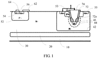
- FIG. 1 is a schematic view of a lateral insulated-gate bipolar transistor according to one embodiment.
- the lateral insulated-gate bipolar transistor includes a substrate 10, an anode terminal and a cathode terminal formed on the substrate 10, and a drift region 30 and a gate 62 located between the anode terminal and the cathode terminal (a gate oxide layer at a bottom of the gate 62 is omitted in FIG. 1 ).
- the anode terminal includes an N-type buffer region 42 on the substrate 10, a P well 44 in the N-type buffer region 42, an N+ region 46 in the P well 44, a trench located above the N+ region 46 and partially surrounded by the P well 44, a polysilicon 74 in the trench, P+ junctions 53 at both sides of the trench, and N+ junctions 55 at both sides of the P+ junction 53.
- the cathode terminal includes a P- region 52 on the substrate 10, a P-type body region 54 and an emitter N+ region 56 in the P- region 52, and a cathode metal 64 serves as an electrode of the emitter.
- the gate 62 when the gate 62 is forward biased, the device channel is turned on, the electron current flows from the N+ region 56 of the emitter, passes through the channel of the P- region 52, and enters the drift region 30, the N-type buffer region 42, and the N+ region 46.
- the collector When the collector is forward biased, the holes begin to be injected into the N-type buffer region 42 through a large area of the PN junction from the P well 44 of the collector, thereby achieving high-efficient multi-path majority carrier holes injection and greatly reducing the on-resistance.
- the collector (including the P+ junction 53 and the N+ junction 55) is forward biased, the N+ region 46, the P well 44, and the N-type buffer region 42 form a lower resistance path for hole injection, which starts to quickly extract the remaining minority carrier holes in the drift region 30, such that a faster switching speed is guaranteed, and the purpose of quick turning off can be achieved.
- the trench is a structure gradually increased in width from bottom to top to form a slope and having a narrow bottom and a wide top.
- a dopant concentration of the N-type buffer region 42 is less than a dopant concentration of the P well 44, and the dopant concentration of the P well 44 is less than dopant concentrations of the P+ junction 53 and the N+ junction 55.
- the dopant concentration of the N-type buffer region 42 ranges from 2E 15 to 5E 15 cm -3
- the dopant concentration of the P well 44 ranges from 4E 17 to 8E 17 cm -3
- the dopant concentrations of the P+ junction 53 and the N+ junction 55 range from 5E 20 to 10E 20 cm -3 .
- the anode terminal further includes an oxide layer located on an inner surface of the trench.
- the oxide layer includes an oxide film 72 located on a sidewall of the trench and spacer structures 72a located at both sides of the bottom of the trench.
- the oxide layer has a void at a position corresponding to a middle portion of the bottom of the trench, such that the polysilicon 74 in the trench is in direct contact with the N+ region 46 below.
- the polysilicon 74 located at both sides of the bottom of the trench is an N+ heavily doped polysilicon, and the dopant concentration is in an order of E 21 to E 22 cm -3 .
- Silicon-on-insulator (SOI) technology is becoming increasingly important in HVIC and SPIC applications, while the IGBT device has gradually played an important role in the field of power device applications due to its low on-resistance characteristics caused by high input impedance and conductivity modulation effect.
- the LIGBT device of SOI type achieves an increasing application in the automotive electronics, home electronics and communications and industrial applications due to its features of low current leakage, low on-state resistance, high input impedance, high package density, fast switching, significant noise reduction effect and feasibility under high temperature work caused by trench isolation.
- the LIGBT shown in FIG. 1 is a silicon on insulator type lateral insulated-gate bipolar transistor (SOI-LIGBT), which includes a buried oxide layer 20 located between the substrate 10 and the drift region 30.
- the substrate 10 is a P-type substrate, and the drift region 30 is an N-type drift region.
- FIG. 2 is a flow chart of a method of manufacturing a lateral insulated-gate bipolar transistor according to one embodiment, which includes:
- step S210 N-type ions are implanted into a silicon wafer, and a drive-in is performed to form an N-type buffer region.
- step S220 a hard mask layer is deposited, and trench lithography and etching are performed to etch the hard mask layer to form a trench window.
- the hard mask layer is deposited on a surface of the silicon wafer, and a photoresist is coated on a surface of the hard mask layer to perform lithography.
- the hard mask exposed under the photoresist after lithography is etched away to form a trench window, thereby exposing the underlying silicon.
- the hard mask layer is a silicon nitride layer. In alternative embodiments, other hard masks known in the art can also be used.
- a pad oxide layer is also formed prior to deposition of the hard mask layer.
- step S230 silicon below the trench window is etched to form a trench.
- etching is performed to form a structure gradually decreased in width from top to bottom to form a slope and having a wide top and a narrow bottom.
- step S240 a liner oxidation is performed to form a liner oxide layer on an inner surface of the trench.
- step S250 P-type ions are implanted, and a P well is formed within an N-type buffer region around the trench.
- the P-type ions are implanted through the trench window, and the ions pass through the oxide layer and form the P well within the N-type buffer region around the trench. Since the thickness of the oxide layer at the sidewall of the trench is greater than the thickness of the oxide layer at the bottom, the concentration distribution of the P-type ions in the P well will be affected accordingly.
- step S260 an oxide layer is deposited in the trench.
- An oxide film is formed on the sidewall of the trench, and spacer structures are formed at both sides of the bottom of the trench after etching the oxide layer.
- a chemical vapor deposition is performed using ethyl orthosilicate (TEOS) as a reactant to form a silicon dioxide layer.
- TEOS ethyl orthosilicate
- oxide layers can also be formed using other techniques known in the art.
- the oxide film is formed on the sidewall of the trench and the spacer structures are formed at both sides of the bottom of the trench using an anisotropic etching.
- a void of the oxide layer is formed in a middle portion of the bottom of the trench, which serves as a window of N+ implantation in step S270.
- step S270 N-type ions are implanted, and an N+ region is formed by a self-aligned implantation under a blocking of the oxide film and the spacer structures.
- the N-type ions are implanted into the trench, and the N+ region is formed by the self-aligned implantation under the blocking of the oxide film and the spacer structures.
- the N+ region formed by the self-aligned implantation and the P well, as well as the N-type buffer region form a longitudinal vertical NPN, which serves as a critical means of controlling minority carrier lifetime.
- step S280 a polysilicon is deposited in the trench, and the hard mask layer is peeled off after etching the polysilicon.
- the method further includes a step of rinsing the silicon dioxide adjacent to the N+ region, so as to remove the silicon dioxide impurities.
- the polysilicon 74 is N+ heavily doped, and the dopant concentration is in an order of E 21 to E 22 cm -3 .
- step S290 annealing is performed to the P well and the N+ region.
- the thermal annealing is performed to activate the doped ions in the P well, the N+ region, and the like. After the annealing is completed, the manufacturing process in other regions of the device is performed, such as a CMOS process.
- step S310 P+ junctions are formed at both sides of the trench and N+ junctions are formed at both sides of the P+ junction by lithography and etching.
- the annealing is also performed accordingly, and then the subsequent process of the device is performed.
- the implantation in the step S250 is performed by multiple implantations, thus a dopant concentration gradient with slower varying is obtained, which can optimize the distribution morphology of the impurities of the P well, and even achieve a constant dopant concentration in a certain region, and help to increase the magnification of N+/P-/N- triodes and accelerate the extraction speed of the holes.
- FIG. 1 A schematic view of the lateral insulated-gate bipolar transistor manufactured using the aforementioned method is shown in FIG. 1 .
- a plurality of holes are injected during forward conduction, thereby forming a significant conductivity modulation effect to reduce the on-state resistance.
- the N+ region and the N+ junction can quickly absorb the minority carrier holes, thereby greatly reducing turn-off loss.
- the collector of the LIGBT the deep collector P well and the P+ junction are introduced through the trench structure, and the N+ polysilicon and the N+ region are formed.
- the N+ polysilicon and the N+ region are formed.
- forward conduction a wide distribution of electron/hole current channel is formed, thereby improving the current capability.
- the optimized collector helps to collect the minority carrier holes more quickly and reduce the turn-off time.
- the dopant concentration of the N-type buffer region 42 ranges from to 5E 15 cm -3
- the dopant concentration of the P well 44 ranges from 4E 17 to 8E 17 cm -3
- the dopant concentrations of the P+ junction 53 and the N+ junction 55 range from 5E 20 to 10E 20 cm -3 .
Landscapes
- Insulated Gate Type Field-Effect Transistor (AREA)
- Thin Film Transistor (AREA)
- Metal-Oxide And Bipolar Metal-Oxide Semiconductor Integrated Circuits (AREA)
- Electrodes Of Semiconductors (AREA)
Abstract
Description
- The present disclosure relates to semiconductor technologies, and more particularly relates to a lateral insulated-gate bipolar transistor, and a manufacturing method of the lateral insulated-gate bipolar transistor.
- Lateral insulated-gate bipolar transistor (LIGBT) is usually employed as an output stage of high-voltage power-driven integrated circuit. Compared with reducing of the on-resistance by a single carrier of a lateral double diffusion metal-oxide semiconductor field effect transistor (LDMOS), the structure of LIGBT can exhibit a lower on-resistance due to a conductive modulation effect formed by injection of double carriers of both electrons and holes.
- However, when LIGBT is turned off, the drift region of LIGBT has a longer turn-off time due to residual minority carrier holes, so there is a problem of a larger power consumption. Because the on-resistance and the turn-off time are inversely proportional to the hole concentration, how to strike a balance between the on-resistance and the turn-off time has become a direction for continuous improvement of the LIGBT device.
- Accordingly, it is necessary to provide a lateral insulated-gate bipolar transistor and a manufacturing method thereof, which can be turned off quickly on the basis of ensuring low on-resistance.
- A lateral insulated-gate bipolar transistor includes a substrate, an anode terminal and a cathode terminal on the substrate, and a drift region and a gate located between the anode terminal and the cathode terminal. The anode terminal includes an N-type buffer region on the substrate, a P well in the N-type buffer region, an N+ region in the P well, a trench located above the N+ region and partially surrounded by the P well, a polysilicon in the trench, P+ junctions at both sides of the trench, and N+ junctions at both sides of the P+ junction.
- A method of manufacturing a lateral insulated-gate bipolar transistor includes: implanting N-type ions into a silicon wafer, and performing a drive-in to form an N-type buffer region; depositing a hard mask layer on a surface of the silicon wafer, and performing trench lithography and etching using a photoresist to etch the hard mask layer to form a trench window; etching silicon below the trench window to form a trench; performing a liner oxidation to form a liner oxide layer on an inner surface of the trench; wherein a thickness of the liner oxide layer at a sidewall of the trench is greater than a thickness of the liner oxide layer at a bottom of the trench; implanting P-type ions through the trench window, and the ions pass through the oxide layer and form a P well within an N-type buffer region around the trench; depositing an oxide layer in the trench, and forming an oxide film on the sidewall of the trench and a spacer structure at both sides of the bottom of the trench after etching the oxide layer; implanting N-type ions into the trench, and forming an N+ region by a self-aligned implantation under a blocking of the oxide film and the spacer; depositing a polysilicon in the trench, peeling off the hard mask layer after etching the polysilicon; performing annealing to the P well and the N+ region; and forming P+ junctions at both sides of the trench and N+ junctions at both sides of the P+ junction by lithography and etching.
- In the aforementioned lateral insulated-gate bipolar transistor, on the one hand, a plurality of holes are injected during forward conduction, thereby forming a significant conductivity modulation effect to reduce the on-state resistance; on the other hand, when the device is turned off, the N+ region and the N+ junction can quickly absorb the minority carrier holes, thereby greatly reducing turn-off loss.
- Further objects, characteristics and advantages of present disclosure will become apparent from the detailed description of preferred embodiments illustrated in accompanying drawings. The components in the drawings are not necessarily drawn to scale, the emphasis instead being placed upon clearly illustrating the principles of the present disclosure. Moreover, in the drawings, like reference numerals designate corresponding parts throughout the views.
-
FIG. 1 is a cross-sectional view of a lateral insulated-gate bipolar transistor according to one embodiment; and -
FIG. 2 is a flow chart of a method of manufacturing the lateral insulated-gate bipolar transistor according to one embodiment. - Embodiments of the invention are described more fully hereinafter with reference to the accompanying drawings. The various embodiments of the invention may, however, be embodied in many different forms and should not be construed as limited to the embodiments set forth herein. Rather, these embodiments are provided so that this disclosure will be thorough and complete, and will fully convey the scope of the invention to those skilled in the art.
- It will be understood that when an element is referred to as being "fixed" to another element, it can be directly fixed to the other element or intervening elements may be present. Also, when an element is referred to as being "connected" or "coupled" to another element, it can be directly connected or coupled to the other element or intervening elements may be present. As used herein, the terms "vertical", "horizontal", "left", "right" and similar expressions are for illustrative purposes only.
- The semiconductor vocabularies used herein are technical terms commonly used by those skilled in the art. For example, with respect to P-type and N-type impurities, in order to distinguish the dopant concentration, a P+ type simply represents a P-type with heavily doped concentration, a P type represents a P-type with medium doped concentration, and a P- type represents a P-type with lightly doped concentration. An N+ type represents an N-type with heavily doped concentration, an N type represents an N-type with medium doped concentration, and an N- type represents an N-type with lightly doped concentration.
- Unless otherwise defined, all terms (including technical and scientific terms) used herein have the same meaning as commonly understood by one of ordinary skill in the art to which this invention belongs. It will be further understood that terms, such as those defined in commonly used dictionaries, should be interpreted as having a meaning that is consistent with their meaning in the context of the relevant art and will not be interpreted in an idealized or overly formal sense unless expressly so defined herein. The term "and/or" as used herein includes any and all combinations of one or more of the associated listed items.
- Due to the long drift region, along with the low conduction voltage drop due to the conductivity modulation effect, the lateral insulated-gate bipolar transistor technology suffers from problem of long turn-off time caused by remaining minority carriers in the drift region. Therefore, how to strike a balance between the on-state voltage drop and the turn-off time has become a direction for continuous improvement of the lateral insulated-gate bipolar transistor.
-
FIG. 1 is a schematic view of a lateral insulated-gate bipolar transistor according to one embodiment. The lateral insulated-gate bipolar transistor includes asubstrate 10, an anode terminal and a cathode terminal formed on thesubstrate 10, and adrift region 30 and agate 62 located between the anode terminal and the cathode terminal (a gate oxide layer at a bottom of thegate 62 is omitted inFIG. 1 ). The anode terminal includes an N-type buffer region 42 on thesubstrate 10, aP well 44 in the N-type buffer region 42, anN+ region 46 in theP well 44, a trench located above theN+ region 46 and partially surrounded by theP well 44, apolysilicon 74 in the trench,P+ junctions 53 at both sides of the trench, andN+ junctions 55 at both sides of theP+ junction 53. The cathode terminal includes a P-region 52 on thesubstrate 10, a P-type body region 54 and anemitter N+ region 56 in the P-region 52, and acathode metal 64 serves as an electrode of the emitter. - In the aforementioned lateral insulated-gate bipolar transistor, when the
gate 62 is forward biased, the device channel is turned on, the electron current flows from theN+ region 56 of the emitter, passes through the channel of the P-region 52, and enters thedrift region 30, the N-type buffer region 42, and theN+ region 46. When the collector is forward biased, the holes begin to be injected into the N-type buffer region 42 through a large area of the PN junction from theP well 44 of the collector, thereby achieving high-efficient multi-path majority carrier holes injection and greatly reducing the on-resistance. When the LIGBT is turned off inversely, the collector (including theP+ junction 53 and the N+ junction 55) is forward biased, theN+ region 46, theP well 44, and the N-type buffer region 42 form a lower resistance path for hole injection, which starts to quickly extract the remaining minority carrier holes in thedrift region 30, such that a faster switching speed is guaranteed, and the purpose of quick turning off can be achieved. - In the embodiment illustrated in
FIG. 1 , the trench is a structure gradually increased in width from bottom to top to form a slope and having a narrow bottom and a wide top. - In the embodiment illustrated in
FIG. 1 , a dopant concentration of the N-type buffer region 42 is less than a dopant concentration of theP well 44, and the dopant concentration of theP well 44 is less than dopant concentrations of theP+ junction 53 and theN+ junction 55. In one embodiment, the dopant concentration of the N-type buffer region 42 ranges from 2E15 to 5E15 cm-3, the dopant concentration of theP well 44 ranges from 4E17 to 8E17 cm-3, and the dopant concentrations of theP+ junction 53 and theN+ junction 55 range from 5E20 to 10E20 cm-3. - In the embodiment illustrated in
FIG. 1 , the anode terminal further includes an oxide layer located on an inner surface of the trench. The oxide layer includes anoxide film 72 located on a sidewall of the trench andspacer structures 72a located at both sides of the bottom of the trench. The oxide layer has a void at a position corresponding to a middle portion of the bottom of the trench, such that thepolysilicon 74 in the trench is in direct contact with theN+ region 46 below. - In the illustrated embodiment, the
polysilicon 74 located at both sides of the bottom of the trench is an N+ heavily doped polysilicon, and the dopant concentration is in an order of E21 to E22 cm-3. - Silicon-on-insulator (SOI) technology is becoming increasingly important in HVIC and SPIC applications, while the IGBT device has gradually played an important role in the field of power device applications due to its low on-resistance characteristics caused by high input impedance and conductivity modulation effect. Compared to the bulk silicone junction isolated devices, the LIGBT device of SOI type achieves an increasing application in the automotive electronics, home electronics and communications and industrial applications due to its features of low current leakage, low on-state resistance, high input impedance, high package density, fast switching, significant noise reduction effect and feasibility under high temperature work caused by trench isolation. It is particularly important to require an efficient injection of holes and a significant conductive modulation effect to reduce the on-state resistance, but correspondingly increase the turn-off loss caused by that minority carrier holes cannot be annihilated quickly when the device is turned off. The LIGBT shown in
FIG. 1 is a silicon on insulator type lateral insulated-gate bipolar transistor (SOI-LIGBT), which includes a buriedoxide layer 20 located between thesubstrate 10 and thedrift region 30. Thesubstrate 10 is a P-type substrate, and thedrift region 30 is an N-type drift region. -
FIG. 2 is a flow chart of a method of manufacturing a lateral insulated-gate bipolar transistor according to one embodiment, which includes: - In step S210, N-type ions are implanted into a silicon wafer, and a drive-in is performed to form an N-type buffer region.
- In step S220, a hard mask layer is deposited, and trench lithography and etching are performed to etch the hard mask layer to form a trench window.
- The hard mask layer is deposited on a surface of the silicon wafer, and a photoresist is coated on a surface of the hard mask layer to perform lithography. The hard mask exposed under the photoresist after lithography is etched away to form a trench window, thereby exposing the underlying silicon. In the illustrated embodiment, the hard mask layer is a silicon nitride layer. In alternative embodiments, other hard masks known in the art can also be used.
- In one embodiment, a pad oxide layer is also formed prior to deposition of the hard mask layer.
- In step S230, silicon below the trench window is etched to form a trench.
- In the illustrated embodiment, etching is performed to form a structure gradually decreased in width from top to bottom to form a slope and having a wide top and a narrow bottom.
- In step S240, a liner oxidation is performed to form a liner oxide layer on an inner surface of the trench.
- Since the crystal orientations of the sidewall and the bottom of the trench are different, there is a difference in the oxidation rate of the liner oxide layer, and a thickness of the oxide layer at the sidewall is greater than a thickness of the oxide layer at the bottom.
- In step S250, P-type ions are implanted, and a P well is formed within an N-type buffer region around the trench.
- The P-type ions are implanted through the trench window, and the ions pass through the oxide layer and form the P well within the N-type buffer region around the trench. Since the thickness of the oxide layer at the sidewall of the trench is greater than the thickness of the oxide layer at the bottom, the concentration distribution of the P-type ions in the P well will be affected accordingly.
- In step S260, an oxide layer is deposited in the trench. An oxide film is formed on the sidewall of the trench, and spacer structures are formed at both sides of the bottom of the trench after etching the oxide layer.
- In the illustrated embodiment, a chemical vapor deposition is performed using ethyl orthosilicate (TEOS) as a reactant to form a silicon dioxide layer. In alternative embodiments, oxide layers can also be formed using other techniques known in the art. After the deposition, the oxide film is formed on the sidewall of the trench and the spacer structures are formed at both sides of the bottom of the trench using an anisotropic etching. In addition, a void of the oxide layer is formed in a middle portion of the bottom of the trench, which serves as a window of N+ implantation in step S270.
- In step S270, N-type ions are implanted, and an N+ region is formed by a self-aligned implantation under a blocking of the oxide film and the spacer structures.
- The N-type ions are implanted into the trench, and the N+ region is formed by the self-aligned implantation under the blocking of the oxide film and the spacer structures.
- The N+ region formed by the self-aligned implantation and the P well, as well as the N-type buffer region form a longitudinal vertical NPN, which serves as a critical means of controlling minority carrier lifetime.
- In step S280, a polysilicon is deposited in the trench, and the hard mask layer is peeled off after etching the polysilicon.
- The polysilicon is deposited and the redundant polysilicon outside the trench is etched away, and then the hard mask layer is removed. In the illustrated embodiment, prior to the step of depositing the polysilicon, the method further includes a step of rinsing the silicon dioxide adjacent to the N+ region, so as to remove the silicon dioxide impurities.
- In the illustrated embodiment, the
polysilicon 74 is N+ heavily doped, and the dopant concentration is in an order of E21 to E22 cm-3. - In step S290, annealing is performed to the P well and the N+ region.
- The thermal annealing is performed to activate the doped ions in the P well, the N+ region, and the like. After the annealing is completed, the manufacturing process in other regions of the device is performed, such as a CMOS process.
- In step S310, P+ junctions are formed at both sides of the trench and N+ junctions are formed at both sides of the P+ junction by lithography and etching.
- After the implantation is completed, the annealing is also performed accordingly, and then the subsequent process of the device is performed.
- In one embodiment, the implantation in the step S250 is performed by multiple implantations, thus a dopant concentration gradient with slower varying is obtained, which can optimize the distribution morphology of the impurities of the P well, and even achieve a constant dopant concentration in a certain region, and help to increase the magnification of N+/P-/N- triodes and accelerate the extraction speed of the holes.
- A schematic view of the lateral insulated-gate bipolar transistor manufactured using the aforementioned method is shown in
FIG. 1 . In the lateral insulated-gate bipolar transistor, a plurality of holes are injected during forward conduction, thereby forming a significant conductivity modulation effect to reduce the on-state resistance. On the other hand, when the device is turned off, the N+ region and the N+ junction can quickly absorb the minority carrier holes, thereby greatly reducing turn-off loss. In other words, by optimizing the collector of the LIGBT, the deep collector P well and the P+ junction are introduced through the trench structure, and the N+ polysilicon and the N+ region are formed. During forward conduction, a wide distribution of electron/hole current channel is formed, thereby improving the current capability. During reverse blocking, the optimized collector helps to collect the minority carrier holes more quickly and reduce the turn-off time. In one embodiment, the dopant concentration of the N-type buffer region 42 ranges from to 5E15 cm-3, the dopant concentration of the P well 44 ranges from 4E17 to 8E17 cm-3, and the dopant concentrations of theP+ junction 53 and theN+ junction 55 range from 5E20 to 10E20 cm-3. - Although the present disclosure is illustrated and described herein with reference to specific embodiments, the present disclosure is not intended to be limited to the details shown. It is to be noted that, various modifications may be made in the details within the scope and range of equivalents of the claims and without departing from the present disclosure. Therefore, the protection scope of the present disclosure shall be subject to the protection scope of the claims.
Claims (15)
- A lateral insulated-gate bipolar transistor, comprising:a substrate;a cathode terminal located on the substrate;an anode terminal located on the substrate, the anode terminal comprising an N-type buffer region located on the substrate, a P well located in the N-type buffer region, an N+ region located in the P well, a trench located above the N+ region and partially surrounded by the P well, a polysilicon located in the trench, P+ junctions located at both sides of the trench, and N+ junctions located at both sides of the P+ junction;a drift region located between the anode terminal and the cathode terminal; anda gate located between the anode terminal and the cathode terminal.
- The lateral insulated-gate bipolar transistor according to claim 1, wherein the trench is a structure gradually increased in width from bottom to top to form a slope and having a narrow bottom and a wide top.
- The lateral insulated-gate bipolar transistor according to claim 1, wherein a dopant concentration of the N-type buffer region is less than a dopant concentration of the P well, and the dopant concentration of the P well is less than dopant concentrations of the P+ junction and the N+ junction.
- The lateral insulated-gate bipolar transistor according to claim 3, wherein the dopant concentration of the N-type buffer region ranges from to 5E15 cm-3, the dopant concentration of the P well ranges from 4E17 to 8E17 cm-3, and the dopant concentrations of the P+ junction and the N+ junction range from 5E20 to 10E20 cm-3.
- The lateral insulated-gate bipolar transistor according to claim 1, wherein the anode terminal further comprises an oxide layer located on an inner surface of the trench, the oxide layer comprises an oxide film located on a sidewall of the trench and a spacer structure located at both sides of a bottom of the trench, the oxide layer has a void at a position corresponding to a middle portion of the bottom of the trench, such that the polysilicon is in direct contact with the N+ region below.
- The lateral insulated-gate bipolar transistor according to claim 1, wherein a dopant concentration of the polysilicon ranges from 1E21 to 10E22 cm-3.
- The lateral insulated-gate bipolar transistor according to claim 1, wherein the lateral insulated-gate bipolar transistor is a silicon-on-insulator type lateral insulated-gate bipolar transistor; the lateral insulated-gate bipolar transistor further comprises a buried oxide layer located between the substrate and the drift region; the substrate is a P-type substrate, and the drift region is an N-type drift region.
- A method of manufacturing a lateral insulated-gate bipolar transistor, comprising:implanting N-type ions into a silicon wafer, and performing a drive-in to form an N-type buffer region;depositing a hard mask layer on a surface of the silicon wafer, and performing trench lithography and etching using a photoresist to etch the hard mask layer to form a trench window;etching silicon below the trench window to form a trench;performing a liner oxidation to form a liner oxide layer on an inner surface of the trench;wherein a thickness of the liner oxide layer at a sidewall of the trench is greater than a thickness of the liner oxide layer at a bottom of the trench;implanting P-type ions through the trench window, and the ions pass through the oxide layer and form a P well within an N-type buffer region around the trench;depositing an oxide layer in the trench, and forming an oxide film on the sidewall of the trench and a spacer structure at both sides of the bottom of the trench after etching the oxide layer;implanting N-type ions into the trench, and forming an N+ region by a self-aligned implantation under a blocking of the oxide film and the spacer;depositing a polysilicon in the trench, peeling off the hard mask layer after etching the polysilicon;performing annealing to the P well and the N+ region; andforming P+ junctions at both sides of the trench and N+ junctions at both sides of the P+ junction by lithography and etching.
- The method according to claim 8, wherein the hard mask layer is a silicon nitride layer.
- The method according to claim 8, wherein during the step of depositing the oxide layer in the trench, and forming the oxide film on the sidewall of the trench and the spacer structure at both sides of the bottom of the trench after etching the oxide layer, a chemical vapor deposition is performed using ethyl orthosilicate as a reactant, and an anisotropic etching is performed.
- The method according to claim 8, wherein, prior to the step of depositing the polysilicon in the trench, and after the step of implanting the N-type ions into the trench, the method further comprises a step of rinsing the oxide layer.
- The method according to claim 8, wherein during the step of implanting the P-type ions through the trench window, and the ions pass through the oxide layer and form the P well within the N-type buffer region around the trench, multiple implantations are performed to obtain a dopant concentration gradient with slower varying.
- The method according to claim 8, wherein a dopant concentration of the N-type buffer region is less than a dopant concentration of the P well, and the dopant concentration of the P well is less than dopant concentrations of the P+ junction and the N+ junction.
- The method according to claim 8, wherein a dopant concentration of the N-type buffer region ranges from to 5E15 cm-3, a dopant concentration of the P well ranges from 4E17 to 8E17 cm-3, and dopant concentrations of the P+ junction and the N+ junction range from 5E20 to 10E20 cm-3.
- The method according to claim 8, wherein the lateral insulated-gate bipolar transistor is a silicon-on-insulator type lateral insulated-gate bipolar transistor; a substrate is a P-type substrate, and a drift region is an N-type drift region.
Applications Claiming Priority (2)
| Application Number | Priority Date | Filing Date | Title |
|---|---|---|---|
| CN201610452720.0A CN107527811B (en) | 2016-06-21 | 2016-06-21 | Lateral insulated gate bipolar transistor and manufacturing method thereof |
| PCT/CN2017/089279 WO2017219968A1 (en) | 2016-06-21 | 2017-06-21 | Lateral insulated-gate bipolar transistor and manufacturing method therefor |
Publications (3)
| Publication Number | Publication Date |
|---|---|
| EP3474330A1 true EP3474330A1 (en) | 2019-04-24 |
| EP3474330A4 EP3474330A4 (en) | 2020-01-22 |
| EP3474330B1 EP3474330B1 (en) | 2022-05-25 |
Family
ID=60734051
Family Applications (1)
| Application Number | Title | Priority Date | Filing Date |
|---|---|---|---|
| EP17814706.2A Active EP3474330B1 (en) | 2016-06-21 | 2017-06-21 | Lateral insulated-gate bipolar transistor and manufacturing method therefor |
Country Status (6)
| Country | Link |
|---|---|
| US (1) | US10770572B2 (en) |
| EP (1) | EP3474330B1 (en) |
| JP (1) | JP6806805B2 (en) |
| KR (1) | KR102158345B1 (en) |
| CN (1) | CN107527811B (en) |
| WO (1) | WO2017219968A1 (en) |
Families Citing this family (6)
| Publication number | Priority date | Publication date | Assignee | Title |
|---|---|---|---|---|
| CN106158956B (en) * | 2015-04-08 | 2020-02-11 | 无锡华润上华科技有限公司 | LDMOSFET with RESURF structure and manufacturing method thereof |
| CN109728083A (en) * | 2018-12-03 | 2019-05-07 | 珠海格力电器股份有限公司 | Insulated gate bipolar transistor, method for making the same, and electrical equipment |
| KR102717707B1 (en) * | 2020-02-06 | 2024-10-16 | 한국전력공사 | Asymmentric trench mosfet device |
| CN115483281B (en) * | 2021-05-31 | 2025-10-03 | 无锡华润上华科技有限公司 | Reverse-conducting lateral insulated gate bipolar transistor |
| CN113555416B (en) * | 2021-09-22 | 2021-12-31 | 四川上特科技有限公司 | A power diode device |
| CN113793804B (en) * | 2021-11-15 | 2022-02-22 | 微龛(广州)半导体有限公司 | Transverse insulated gate bipolar transistor structure and preparation method thereof |
Family Cites Families (15)
| Publication number | Priority date | Publication date | Assignee | Title |
|---|---|---|---|---|
| US6313000B1 (en) * | 1999-11-18 | 2001-11-06 | National Semiconductor Corporation | Process for formation of vertically isolated bipolar transistor device |
| US7109551B2 (en) * | 2003-08-29 | 2006-09-19 | Fuji Electric Holdings Co., Ltd. | Semiconductor device |
| JP2005101581A (en) | 2003-08-29 | 2005-04-14 | Fuji Electric Holdings Co Ltd | Semiconductor device |
| JP4725040B2 (en) * | 2004-06-17 | 2011-07-13 | 富士電機システムズ株式会社 | SOI trench lateral IGBT |
| JP2006054248A (en) * | 2004-08-10 | 2006-02-23 | Fuji Electric Device Technology Co Ltd | Semiconductor device and manufacturing method thereof |
| DE112005003720T5 (en) | 2005-10-12 | 2008-09-11 | Fuji Electric Holdings Co., Ltd., Kawasaki | SOI trench lateral IGBT |
| US7465964B2 (en) | 2005-12-30 | 2008-12-16 | Cambridge Semiconductor Limited | Semiconductor device in which an injector region is isolated from a substrate |
| CN2914330Y (en) | 2006-05-24 | 2007-06-20 | 杭州电子科技大学 | Anti-ESD integrated SOI LIGBT unit |
| US8354710B2 (en) | 2008-08-08 | 2013-01-15 | Infineon Technologies Ag | Field-effect device and manufacturing method thereof |
| US8253164B2 (en) | 2010-12-23 | 2012-08-28 | Force Mos Technology Co., Ltd. | Fast switching lateral insulated gate bipolar transistor (LIGBT) with trenched contacts |
| CN102148240B (en) * | 2011-03-10 | 2012-08-29 | 电子科技大学 | SOI-LIGBT (silicon on insulator-lateral insulated gate bipolar transistor) device with split anode structure |
| CN102157550B (en) * | 2011-03-10 | 2012-07-04 | 杭州电子科技大学 | SOI (silicon on insulator) LIGBT (lateral insulated gate bipolar transistor) device unit with p buried layer and longitudinal channel |
| US9070735B2 (en) | 2013-07-02 | 2015-06-30 | Cambridge Microelectronics Ltd. | Lateral power semiconductor transistors |
| CN104347397B (en) * | 2013-07-23 | 2018-02-06 | 无锡华润上华科技有限公司 | Inject the manufacture method of reinforced insulation grid bipolar transistor |
| CN105789298B (en) | 2014-12-19 | 2019-06-07 | 无锡华润上华科技有限公司 | Landscape insulation bar double-pole-type transistor and its manufacturing method |
-
2016
- 2016-06-21 CN CN201610452720.0A patent/CN107527811B/en active Active
-
2017
- 2017-06-21 US US16/311,276 patent/US10770572B2/en active Active
- 2017-06-21 EP EP17814706.2A patent/EP3474330B1/en active Active
- 2017-06-21 JP JP2018566861A patent/JP6806805B2/en active Active
- 2017-06-21 WO PCT/CN2017/089279 patent/WO2017219968A1/en not_active Ceased
- 2017-06-21 KR KR1020187036722A patent/KR102158345B1/en active Active
Also Published As
| Publication number | Publication date |
|---|---|
| US20190245069A1 (en) | 2019-08-08 |
| JP6806805B2 (en) | 2021-01-06 |
| EP3474330A4 (en) | 2020-01-22 |
| EP3474330B1 (en) | 2022-05-25 |
| US10770572B2 (en) | 2020-09-08 |
| KR20190008573A (en) | 2019-01-24 |
| JP2019519116A (en) | 2019-07-04 |
| CN107527811A (en) | 2017-12-29 |
| WO2017219968A1 (en) | 2017-12-28 |
| CN107527811B (en) | 2020-07-10 |
| KR102158345B1 (en) | 2020-09-23 |
Similar Documents
| Publication | Publication Date | Title |
|---|---|---|
| US11121242B2 (en) | Method of operating a semiconductor device having a desaturation channel structure | |
| US10770572B2 (en) | Lateral insulated-gate bipolar transistor and manufacturing method therefor | |
| KR101645769B1 (en) | Power semiconductor devices having selectively doped jfet regions and related methods of forming such devices | |
| TWI688095B (en) | Semiconductor structure including a transistor including a gate electrode region provided in a substrate and method for the formation thereof | |
| CN109713037B (en) | Insulated gate bipolar transistor device and preparation method thereof | |
| EP3240042B1 (en) | Lateral insulated-gate bipolar transistor and manufacturing method therefor | |
| CN110914997A (en) | Semiconductor devices with LOCOS trenches | |
| CN103477439A (en) | Semiconductor device and process for production thereof | |
| US12154944B2 (en) | Super junction power device | |
| CN104103690A (en) | Semiconductor device and method for producing the same | |
| US10217828B1 (en) | Transistors with field plates on fully depleted silicon-on-insulator platform and method of making the same | |
| KR20160033202A (en) | Semiconductor device | |
| US12154943B2 (en) | Super junction power device and method of making the same | |
| JP2014112625A (en) | Power semiconductor element and method for manufacturing the same | |
| US10692995B2 (en) | Insulated-gate bipolar transistor structure and method for manufacturing the same | |
| JP6430650B2 (en) | Horizontal insulated gate bipolar transistor | |
| CN111129131A (en) | Planar Gate IGBT Devices | |
| JPH10335630A (en) | Semiconductor device and manufacturing method thereof | |
| CN119230399B (en) | Manufacturing method of IGBT device | |
| KR102141845B1 (en) | power semiconductor device and method of manufacturing the same | |
| CN105097903B (en) | Silicon-on-insulator lateral N-type insulated gate bipolar transistor | |
| CN106098761A (en) | Insulated gate bipolar transistor structure and manufacturing method thereof | |
| JP2006210865A (en) | Semiconductor device | |
| CN121941067A (en) | Semiconductor devices and their fabrication methods | |
| CN118507527A (en) | Double-gate control device and manufacturing method |
Legal Events
| Date | Code | Title | Description |
|---|---|---|---|
| STAA | Information on the status of an ep patent application or granted ep patent |
Free format text: STATUS: THE INTERNATIONAL PUBLICATION HAS BEEN MADE |
|
| PUAI | Public reference made under article 153(3) epc to a published international application that has entered the european phase |
Free format text: ORIGINAL CODE: 0009012 |
|
| STAA | Information on the status of an ep patent application or granted ep patent |
Free format text: STATUS: REQUEST FOR EXAMINATION WAS MADE |
|
| 17P | Request for examination filed |
Effective date: 20181219 |
|
| AK | Designated contracting states |
Kind code of ref document: A1 Designated state(s): AL AT BE BG CH CY CZ DE DK EE ES FI FR GB GR HR HU IE IS IT LI LT LU LV MC MK MT NL NO PL PT RO RS SE SI SK SM TR |
|
| AX | Request for extension of the european patent |
Extension state: BA ME |
|
| DAV | Request for validation of the european patent (deleted) | ||
| DAX | Request for extension of the european patent (deleted) | ||
| A4 | Supplementary search report drawn up and despatched |
Effective date: 20200103 |
|
| RIC1 | Information provided on ipc code assigned before grant |
Ipc: H01L 29/40 20060101ALI20191218BHEP Ipc: H01L 29/06 20060101ALI20191218BHEP Ipc: H01L 21/331 20060101ALI20191218BHEP Ipc: H01L 29/739 20060101AFI20191218BHEP Ipc: H01L 29/08 20060101ALI20191218BHEP |
|
| STAA | Information on the status of an ep patent application or granted ep patent |
Free format text: STATUS: EXAMINATION IS IN PROGRESS |
|
| 17Q | First examination report despatched |
Effective date: 20210422 |
|
| GRAP | Despatch of communication of intention to grant a patent |
Free format text: ORIGINAL CODE: EPIDOSNIGR1 |
|
| STAA | Information on the status of an ep patent application or granted ep patent |
Free format text: STATUS: GRANT OF PATENT IS INTENDED |
|
| INTG | Intention to grant announced |
Effective date: 20211209 |
|
| GRAS | Grant fee paid |
Free format text: ORIGINAL CODE: EPIDOSNIGR3 |
|
| GRAA | (expected) grant |
Free format text: ORIGINAL CODE: 0009210 |
|
| STAA | Information on the status of an ep patent application or granted ep patent |
Free format text: STATUS: THE PATENT HAS BEEN GRANTED |
|
| AK | Designated contracting states |
Kind code of ref document: B1 Designated state(s): AL AT BE BG CH CY CZ DE DK EE ES FI FR GB GR HR HU IE IS IT LI LT LU LV MC MK MT NL NO PL PT RO RS SE SI SK SM TR |
|
| REG | Reference to a national code |
Ref country code: GB Ref legal event code: FG4D |
|
| REG | Reference to a national code |
Ref country code: CH Ref legal event code: EP |
|
| REG | Reference to a national code |
Ref country code: AT Ref legal event code: REF Ref document number: 1494603 Country of ref document: AT Kind code of ref document: T Effective date: 20220615 Ref country code: DE Ref legal event code: R096 Ref document number: 602017057857 Country of ref document: DE |
|
| REG | Reference to a national code |
Ref country code: IE Ref legal event code: FG4D |
|
| REG | Reference to a national code |
Ref country code: NL Ref legal event code: FP |
|
| REG | Reference to a national code |
Ref country code: LT Ref legal event code: MG9D |
|
| REG | Reference to a national code |
Ref country code: AT Ref legal event code: MK05 Ref document number: 1494603 Country of ref document: AT Kind code of ref document: T Effective date: 20220525 |
|
| PG25 | Lapsed in a contracting state [announced via postgrant information from national office to epo] |
Ref country code: SE Free format text: LAPSE BECAUSE OF FAILURE TO SUBMIT A TRANSLATION OF THE DESCRIPTION OR TO PAY THE FEE WITHIN THE PRESCRIBED TIME-LIMIT Effective date: 20220525 Ref country code: PT Free format text: LAPSE BECAUSE OF FAILURE TO SUBMIT A TRANSLATION OF THE DESCRIPTION OR TO PAY THE FEE WITHIN THE PRESCRIBED TIME-LIMIT Effective date: 20220926 Ref country code: NO Free format text: LAPSE BECAUSE OF FAILURE TO SUBMIT A TRANSLATION OF THE DESCRIPTION OR TO PAY THE FEE WITHIN THE PRESCRIBED TIME-LIMIT Effective date: 20220825 Ref country code: LT Free format text: LAPSE BECAUSE OF FAILURE TO SUBMIT A TRANSLATION OF THE DESCRIPTION OR TO PAY THE FEE WITHIN THE PRESCRIBED TIME-LIMIT Effective date: 20220525 Ref country code: HR Free format text: LAPSE BECAUSE OF FAILURE TO SUBMIT A TRANSLATION OF THE DESCRIPTION OR TO PAY THE FEE WITHIN THE PRESCRIBED TIME-LIMIT Effective date: 20220525 Ref country code: GR Free format text: LAPSE BECAUSE OF FAILURE TO SUBMIT A TRANSLATION OF THE DESCRIPTION OR TO PAY THE FEE WITHIN THE PRESCRIBED TIME-LIMIT Effective date: 20220826 Ref country code: FI Free format text: LAPSE BECAUSE OF FAILURE TO SUBMIT A TRANSLATION OF THE DESCRIPTION OR TO PAY THE FEE WITHIN THE PRESCRIBED TIME-LIMIT Effective date: 20220525 Ref country code: ES Free format text: LAPSE BECAUSE OF FAILURE TO SUBMIT A TRANSLATION OF THE DESCRIPTION OR TO PAY THE FEE WITHIN THE PRESCRIBED TIME-LIMIT Effective date: 20220525 Ref country code: BG Free format text: LAPSE BECAUSE OF FAILURE TO SUBMIT A TRANSLATION OF THE DESCRIPTION OR TO PAY THE FEE WITHIN THE PRESCRIBED TIME-LIMIT Effective date: 20220825 Ref country code: AT Free format text: LAPSE BECAUSE OF FAILURE TO SUBMIT A TRANSLATION OF THE DESCRIPTION OR TO PAY THE FEE WITHIN THE PRESCRIBED TIME-LIMIT Effective date: 20220525 |
|
| PG25 | Lapsed in a contracting state [announced via postgrant information from national office to epo] |
Ref country code: RS Free format text: LAPSE BECAUSE OF FAILURE TO SUBMIT A TRANSLATION OF THE DESCRIPTION OR TO PAY THE FEE WITHIN THE PRESCRIBED TIME-LIMIT Effective date: 20220525 Ref country code: PL Free format text: LAPSE BECAUSE OF FAILURE TO SUBMIT A TRANSLATION OF THE DESCRIPTION OR TO PAY THE FEE WITHIN THE PRESCRIBED TIME-LIMIT Effective date: 20220525 Ref country code: LV Free format text: LAPSE BECAUSE OF FAILURE TO SUBMIT A TRANSLATION OF THE DESCRIPTION OR TO PAY THE FEE WITHIN THE PRESCRIBED TIME-LIMIT Effective date: 20220525 Ref country code: IS Free format text: LAPSE BECAUSE OF FAILURE TO SUBMIT A TRANSLATION OF THE DESCRIPTION OR TO PAY THE FEE WITHIN THE PRESCRIBED TIME-LIMIT Effective date: 20220925 |
|
| PG25 | Lapsed in a contracting state [announced via postgrant information from national office to epo] |
Ref country code: SM Free format text: LAPSE BECAUSE OF FAILURE TO SUBMIT A TRANSLATION OF THE DESCRIPTION OR TO PAY THE FEE WITHIN THE PRESCRIBED TIME-LIMIT Effective date: 20220525 Ref country code: SK Free format text: LAPSE BECAUSE OF FAILURE TO SUBMIT A TRANSLATION OF THE DESCRIPTION OR TO PAY THE FEE WITHIN THE PRESCRIBED TIME-LIMIT Effective date: 20220525 Ref country code: RO Free format text: LAPSE BECAUSE OF FAILURE TO SUBMIT A TRANSLATION OF THE DESCRIPTION OR TO PAY THE FEE WITHIN THE PRESCRIBED TIME-LIMIT Effective date: 20220525 Ref country code: EE Free format text: LAPSE BECAUSE OF FAILURE TO SUBMIT A TRANSLATION OF THE DESCRIPTION OR TO PAY THE FEE WITHIN THE PRESCRIBED TIME-LIMIT Effective date: 20220525 Ref country code: DK Free format text: LAPSE BECAUSE OF FAILURE TO SUBMIT A TRANSLATION OF THE DESCRIPTION OR TO PAY THE FEE WITHIN THE PRESCRIBED TIME-LIMIT Effective date: 20220525 Ref country code: CZ Free format text: LAPSE BECAUSE OF FAILURE TO SUBMIT A TRANSLATION OF THE DESCRIPTION OR TO PAY THE FEE WITHIN THE PRESCRIBED TIME-LIMIT Effective date: 20220525 |
|
| REG | Reference to a national code |
Ref country code: CH Ref legal event code: PL |
|
| REG | Reference to a national code |
Ref country code: BE Ref legal event code: MM Effective date: 20220630 |
|
| PG25 | Lapsed in a contracting state [announced via postgrant information from national office to epo] |
Ref country code: MC Free format text: LAPSE BECAUSE OF FAILURE TO SUBMIT A TRANSLATION OF THE DESCRIPTION OR TO PAY THE FEE WITHIN THE PRESCRIBED TIME-LIMIT Effective date: 20220525 |
|
| REG | Reference to a national code |
Ref country code: DE Ref legal event code: R097 Ref document number: 602017057857 Country of ref document: DE |
|
| PG25 | Lapsed in a contracting state [announced via postgrant information from national office to epo] |
Ref country code: AL Free format text: LAPSE BECAUSE OF FAILURE TO SUBMIT A TRANSLATION OF THE DESCRIPTION OR TO PAY THE FEE WITHIN THE PRESCRIBED TIME-LIMIT Effective date: 20220525 |
|
| PLBE | No opposition filed within time limit |
Free format text: ORIGINAL CODE: 0009261 |
|
| STAA | Information on the status of an ep patent application or granted ep patent |
Free format text: STATUS: NO OPPOSITION FILED WITHIN TIME LIMIT |
|
| PG25 | Lapsed in a contracting state [announced via postgrant information from national office to epo] |
Ref country code: LU Free format text: LAPSE BECAUSE OF NON-PAYMENT OF DUE FEES Effective date: 20220621 Ref country code: LI Free format text: LAPSE BECAUSE OF NON-PAYMENT OF DUE FEES Effective date: 20220630 Ref country code: IE Free format text: LAPSE BECAUSE OF NON-PAYMENT OF DUE FEES Effective date: 20220621 Ref country code: CH Free format text: LAPSE BECAUSE OF NON-PAYMENT OF DUE FEES Effective date: 20220630 |
|
| 26N | No opposition filed |
Effective date: 20230228 |
|
| PG25 | Lapsed in a contracting state [announced via postgrant information from national office to epo] |
Ref country code: SI Free format text: LAPSE BECAUSE OF FAILURE TO SUBMIT A TRANSLATION OF THE DESCRIPTION OR TO PAY THE FEE WITHIN THE PRESCRIBED TIME-LIMIT Effective date: 20220525 Ref country code: BE Free format text: LAPSE BECAUSE OF NON-PAYMENT OF DUE FEES Effective date: 20220630 |
|
| PG25 | Lapsed in a contracting state [announced via postgrant information from national office to epo] |
Ref country code: IT Free format text: LAPSE BECAUSE OF FAILURE TO SUBMIT A TRANSLATION OF THE DESCRIPTION OR TO PAY THE FEE WITHIN THE PRESCRIBED TIME-LIMIT Effective date: 20220525 |
|
| PG25 | Lapsed in a contracting state [announced via postgrant information from national office to epo] |
Ref country code: HU Free format text: LAPSE BECAUSE OF FAILURE TO SUBMIT A TRANSLATION OF THE DESCRIPTION OR TO PAY THE FEE WITHIN THE PRESCRIBED TIME-LIMIT; INVALID AB INITIO Effective date: 20170621 |
|
| PG25 | Lapsed in a contracting state [announced via postgrant information from national office to epo] |
Ref country code: MK Free format text: LAPSE BECAUSE OF FAILURE TO SUBMIT A TRANSLATION OF THE DESCRIPTION OR TO PAY THE FEE WITHIN THE PRESCRIBED TIME-LIMIT Effective date: 20220525 Ref country code: CY Free format text: LAPSE BECAUSE OF FAILURE TO SUBMIT A TRANSLATION OF THE DESCRIPTION OR TO PAY THE FEE WITHIN THE PRESCRIBED TIME-LIMIT Effective date: 20220525 |
|
| PG25 | Lapsed in a contracting state [announced via postgrant information from national office to epo] |
Ref country code: TR Free format text: LAPSE BECAUSE OF FAILURE TO SUBMIT A TRANSLATION OF THE DESCRIPTION OR TO PAY THE FEE WITHIN THE PRESCRIBED TIME-LIMIT Effective date: 20220525 |
|
| PG25 | Lapsed in a contracting state [announced via postgrant information from national office to epo] |
Ref country code: MT Free format text: LAPSE BECAUSE OF FAILURE TO SUBMIT A TRANSLATION OF THE DESCRIPTION OR TO PAY THE FEE WITHIN THE PRESCRIBED TIME-LIMIT Effective date: 20220525 |
|
| PG25 | Lapsed in a contracting state [announced via postgrant information from national office to epo] |
Ref country code: BG Free format text: LAPSE BECAUSE OF FAILURE TO SUBMIT A TRANSLATION OF THE DESCRIPTION OR TO PAY THE FEE WITHIN THE PRESCRIBED TIME-LIMIT Effective date: 20220525 |
|
| REG | Reference to a national code |
Ref country code: DE Ref legal event code: R079 Ref document number: 602017057857 Country of ref document: DE Free format text: PREVIOUS MAIN CLASS: H01L0029739000 Ipc: H10D0012000000 |
|
| PG25 | Lapsed in a contracting state [announced via postgrant information from national office to epo] |
Ref country code: BG Free format text: LAPSE BECAUSE OF FAILURE TO SUBMIT A TRANSLATION OF THE DESCRIPTION OR TO PAY THE FEE WITHIN THE PRESCRIBED TIME-LIMIT Effective date: 20220525 |
|
| PGFP | Annual fee paid to national office [announced via postgrant information from national office to epo] |
Ref country code: NL Payment date: 20250314 Year of fee payment: 9 |
|
| PGFP | Annual fee paid to national office [announced via postgrant information from national office to epo] |
Ref country code: FR Payment date: 20250305 Year of fee payment: 9 |
|
| PGFP | Annual fee paid to national office [announced via postgrant information from national office to epo] |
Ref country code: DE Payment date: 20250618 Year of fee payment: 9 |
|
| PGFP | Annual fee paid to national office [announced via postgrant information from national office to epo] |
Ref country code: GB Payment date: 20250402 Year of fee payment: 9 |