EP3472864B1 - Semiconductor device sub-assembly and manufacturing method thereof - Google Patents
Semiconductor device sub-assembly and manufacturing method thereof Download PDFInfo
- Publication number
- EP3472864B1 EP3472864B1 EP17701919.7A EP17701919A EP3472864B1 EP 3472864 B1 EP3472864 B1 EP 3472864B1 EP 17701919 A EP17701919 A EP 17701919A EP 3472864 B1 EP3472864 B1 EP 3472864B1
- Authority
- EP
- European Patent Office
- Prior art keywords
- conductive
- sub
- malleable layer
- assembly
- semiconductor
- Prior art date
- Legal status (The legal status is an assumption and is not a legal conclusion. Google has not performed a legal analysis and makes no representation as to the accuracy of the status listed.)
- Active
Links
Images


Classifications
-
- H—ELECTRICITY
- H10—SEMICONDUCTOR DEVICES; ELECTRIC SOLID-STATE DEVICES NOT OTHERWISE PROVIDED FOR
- H10W—GENERIC PACKAGES, INTERCONNECTIONS, CONNECTORS OR OTHER CONSTRUCTIONAL DETAILS OF DEVICES COVERED BY CLASS H10
- H10W90/00—Package configurations
- H10W90/701—Package configurations characterised by the relative positions of pads or connectors relative to package parts
-
- H—ELECTRICITY
- H10—SEMICONDUCTOR DEVICES; ELECTRIC SOLID-STATE DEVICES NOT OTHERWISE PROVIDED FOR
- H10W—GENERIC PACKAGES, INTERCONNECTIONS, CONNECTORS OR OTHER CONSTRUCTIONAL DETAILS OF DEVICES COVERED BY CLASS H10
- H10W70/00—Package substrates; Interposers; Redistribution layers [RDL]
- H10W70/60—Insulating or insulated package substrates; Interposers; Redistribution layers
- H10W70/62—Insulating or insulated package substrates; Interposers; Redistribution layers characterised by their interconnections
- H10W70/65—Shapes or dispositions of interconnections
- H10W70/658—Shapes or dispositions of interconnections for devices provided for in groups H10D8/00 - H10D48/00
-
- H—ELECTRICITY
- H10—SEMICONDUCTOR DEVICES; ELECTRIC SOLID-STATE DEVICES NOT OTHERWISE PROVIDED FOR
- H10W—GENERIC PACKAGES, INTERCONNECTIONS, CONNECTORS OR OTHER CONSTRUCTIONAL DETAILS OF DEVICES COVERED BY CLASS H10
- H10W72/00—Interconnections or connectors in packages
-
- H—ELECTRICITY
- H10—SEMICONDUCTOR DEVICES; ELECTRIC SOLID-STATE DEVICES NOT OTHERWISE PROVIDED FOR
- H10W—GENERIC PACKAGES, INTERCONNECTIONS, CONNECTORS OR OTHER CONSTRUCTIONAL DETAILS OF DEVICES COVERED BY CLASS H10
- H10W72/00—Interconnections or connectors in packages
- H10W72/01—Manufacture or treatment
- H10W72/0198—Manufacture or treatment batch processes
-
- H—ELECTRICITY
- H10—SEMICONDUCTOR DEVICES; ELECTRIC SOLID-STATE DEVICES NOT OTHERWISE PROVIDED FOR
- H10W—GENERIC PACKAGES, INTERCONNECTIONS, CONNECTORS OR OTHER CONSTRUCTIONAL DETAILS OF DEVICES COVERED BY CLASS H10
- H10W76/00—Containers; Fillings or auxiliary members therefor; Seals
- H10W76/10—Containers or parts thereof
- H10W76/12—Containers or parts thereof characterised by their shape
- H10W76/13—Containers comprising a conductive base serving as an interconnection
- H10W76/138—Containers comprising a conductive base serving as an interconnection having another interconnection being formed by a cover plate parallel to the conductive base, e.g. sandwich type
-
- H—ELECTRICITY
- H10—SEMICONDUCTOR DEVICES; ELECTRIC SOLID-STATE DEVICES NOT OTHERWISE PROVIDED FOR
- H10W—GENERIC PACKAGES, INTERCONNECTIONS, CONNECTORS OR OTHER CONSTRUCTIONAL DETAILS OF DEVICES COVERED BY CLASS H10
- H10W90/00—Package configurations
Definitions
- the present invention relates to a semiconductor device sub-assembly.
- semiconductor chips are placed between mechanical strain buffers, such as molybdenum or tungsten, to form a semiconductor unit. These semiconductor units are then placed between two common copper electrodes.
- mechanical strain buffers such as molybdenum or tungsten
- the pressure distribution across the chips within the package should be as uniform as possible. This is difficult to achieve, as micron-level differences in semiconductor unit thickness or surface flatness variations across the copper electrodes can lead to applied pressures that differ greatly between semiconductor chips and also differ from the intended target pressure.
- the flatness and parallelism of components, such as heatsinks in the end-users' application will also have a significant effect on this. The effect is amplified in cases where multiple devices are clamped in a single stack for series operation, due to the additive effect of all of the tolerances within the stack.
- the inventor has appreciated that there are applications where up to twenty such devices are clamped in a single stack.
- One approach is to use extremely tightly toleranced components (typically matched to within 1 ⁇ m), to ensure component thicknesses are as closely matched as possible and to dictate that end-users provide clamp components (such as heatsinks and load spreaders) that have a much tighter flatness tolerance for multi-chip pressure contact devices than is used for traditional single chip pressure contact devices, such as large-area thyristors (e.g. typically 10 ⁇ m flatness tolerance, instead of 30 ⁇ m).
- Tight component tolerance ranges become hard to manage with large numbers of components, as is the case in large-area multi-chip pressure contact devices. Tight flatness tolerances for clamping components also become harder to achieve across a large surface area, compounding the problem.
- Another approach is to use individual disc spring stacks in line with each individual semiconductor unit within the housing in order to reduce the force/displacement ratio. In this way, for a given difference in semiconductor unit thicknesses or a given flatness variation, the difference in contact pressure is minimised.
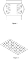
- the disc springs are relatively poor electrical conductors, conductive metallic bypass strips (longitudinal current bypass) or stamped, contoured metal sheets (lateral current bypass) are used. Bypass strips run from the top to the bottom of the stack of disc springs. When the disc springs are compressed, the flexible bypass strip bows outwards. This arrangement is used in ABB's StakPak arrangement which is shown in figure 1 . Due to the outward bow of the bypass strips, the packing density of chips may be limited, in turn limiting the current density of the finished device.
- the stamped, contoured metal sheet is shaped as shown in figure 2 and incorporated in the finished device described in patent number CN103579165 .
- the longitudinal current bypass strip method in figure 1 due to the shaping of the sheet, and the area required to form the sheet, the packing density of chips is limited, again limiting the current density of the finished device.
- a further approach is to use a pressurised fluid to pressurise the contact components in the device. This has been detailed in patent JP2004158489 . This does, however, rely on the availability of pressurised fluid, which is feasible in hybrid vehicles, but less so in typical industrial and transmission and distribution applications.
- the first approach (as used in ABB's StakPak) uses the rigid insulative sleeve of the device housing as a travel-stop mechanism, which prevents depression of the external contact surfaces beyond a defined plane.
- the chips are grouped into sub-modules which contain the spring assemblies. Either four or six sub-modules are used in a finished device, each of which is individually tested before being assembled.
- the device specification requires the load to be sufficient to compress the external contact surfaces level with the top of the sleeve (referred to as the threshold load in this document). Beyond the threshold load, any excess load is supported by the sleeve and the load applied to the chips is then dictated by the load/displacement ratio of the spring system and increases no further, even with extra loading.
- the displacement is defined as the difference between the pre-load height of the spring stack and the loaded height of the spring stack, once the sleeve begins to carry the mechanical load. In this design, only the sleeve supports load above the threshold load around the perimeter of the device, with no mechanical support provided in the centre of the device.
- CN103579165 uses a rigid insulative support frame inside the device housing to act as a travel stop mechanism. This acts in a similar manner to the perimeter travel stop mechanism described above. From the images given, it appears that load above the threshold load is supported in the centre of the device as well as at the edge. For this design to be tested or operated, the entire device must be fully assembled. Operation as a subassembly is not possible.
- US 5,828,564 relates to rectifier heat dissipation.
- the conductive device includes a metal base serving as one electrode and having a side surface portion and a seating surface portion and a metal heat dissipation member including a socket section for receiving metal base.
- US 5,874,774 relates to a semiconductor device which includes a plurality of semiconductor chips each of which has a first main electrode and a control electrode on a first main surface and a second main electrode on a second main surface, and a plurality of support plates each of which is secured to the second main surface of the corresponding semiconductor chip.
- US 4,224,663 relates to a mounting assembly for pass-pack semiconductive controlled rectifiers.
- US 5,994,773 relates to a ball grid array semiconductor package.
- US 5,990,501 relates to a multichip press-contact type semiconductor device, including a plurality of semiconductor chips, a plurality of heat buffer plates, a conductive metal sheet, and first and second press-contact electrode plates.
- a substantially uniform pressure distribution is achieved by flexing the malleable layer to a predetermined level.
- the invention presented here is a unique solution to the problem of improving pressure uniformity across a power device, e.g. a press-pack IGBT device. It greatly simplifies the assembly process. It allows chips to be packed very densely (and so a higher overall current rating per device).
- the sub-assembly further comprises a stand-off plate operatively connected with an opposing surface of the conductive malleable layer compared to a surface of the conductive malleable layer to which the conductive block is coupled.
- the conductive block is generally in contact with a first surface of the malleable layer and the stand-off plate is coupled with a second opposing surface of the malleable layer.
- the stand-off plate comprises a plurality of holes or voids.
- the conductive malleable layer is flexed into each hole of the stand-off plate by each conductive block. This flexing technique helps to provide substantially uniform pressure distribution across all the devices of the sub-assembly.
- the thickness of the conductive malleable layer is chosen such that the conductive malleable layer is at least elastically deformed.
- the yield strength of a material of the conductive malleable layer is chosen such that the conductive malleable layer is at least plastically deformed by the conductive block under the applied pressure.
- the conductive malleable layer may be at least plastically deformed at an elevated temperature between -50°c and 150°C.
- the conductive malleable layer may be a flat diaphragm.
- the conductive malleable layer is a continuous layer, preferably without any contoured hole or recess into it.
- the thickness of the conductive malleable layer may be from about 0.1 mm to 10 mm.
- the conductive malleable layer may comprise a material comprising copper, stainless steel, aluminium, silver, or an alloy of copper, aluminium, stainless steel and silver.
- the conductive block may comprise a material comprising copper, aluminium, silver, or an alloy of copper, aluminium, and silver.
- the stand-off plate may comprise a material comprising copper, aluminium, silver, or an alloy of copper, aluminium, and silver.
- the stand-off plate, conductive malleable layer and conductive blocks may be formed using one piece of material.
- the sub-assembly may further comprise a printed circuit board on the conductive malleable layer, the printed circuit board is configured to distribute a control signal applied to a control terminal of the semiconductor unit.
- the printed circuit board may comprise a plurality of holes, each hole being aligned with each hole of the stand-off plate. Each conductive block may be located in each hole of the printed circuit board.
- the sub-assembly is configured such that after the pressure is applied a conductive path is established through the semiconductor unit, conductive block, conductive malleable layer, and stand-off plate.
- the semiconductor unit may comprise:
- the backside strain buffer may be a disc covering all the chips within the sub-assembly.
- the backside strain buffer may comprise any one of aluminium-graphite, molybdenum and molybdenum-copper.
- the sub-assembly may further comprise a metal layer between the semiconductor chip and the frontside and backside strain buffers
- the front side strain buffer and the back side strain buffer may be attached to the semiconductor chip by a soldering technique.
- the front side strain buffer and the back side strain buffer may be attached to the semiconductor chip by a silver sintering technique.
- the sub-assembly may have a square or circular shape.
- the sub-assembly may further comprise a deflection limiting frame between the conductive malleable layer and semiconductor unit.
- the deflection limiting frame may comprise polyether ether ketone (PEEK).
- Individual semiconductor chips can be connected in parallel within a single pressure contact housing to provide a single device containing multiple chips with a current handling capability that is ideally the sum of the capability of all the chips contained within the housing.
- the conductive malleable layer may be a flat diaphragm.
- the conductive malleable layer may be a continuous layer without a contoured area in the malleable layer.
- the conductive malleable layer may be a flexible layer.
- the conductive malleable layer may comprise a material comprising copper, aluminium, silver and an alloy of copper, aluminium and silver.
- the sub-assembly may further comprise a printed circuit board on the conductive malleable layer, the printed circuit board is configured to distribute a control signal applied to a control terminal of the semiconductor unit.
- the semiconductor unit may comprise:
- Figure 4 illustrates a three-dimensional view of a finished semiconductor unit that may incorporate a sub-assembly in accordance with teone embodiment of the present invention.
- Figure 5 illustrates a schematic cross-section of the semiconductor unit of Figure 4 .
- the semiconductor unit includes a semiconductor chip 2, for example, an insulated gate bipolar transistor (IGBT), metal oxide semiconductor field effect transistor (MOSFET), bipolar junction transistor (BJT) or any other type of semiconductor devices.
- the unit includes a frontside strain buffer 4 and a backside strain buffer 5.
- the unit 1 also includes a control terminal connection spring pin 6.
- the unit 1 also includes a moulded locator 3 that serves to locate the frontside strain buffer 4, backside strain buffer 5 and control terminal connection spring pin 6 relative to the semiconductor chip 2.
- the backside strain buffer 5 may not be an individual component for each chip, but may be one large disc of this material that covers all of the chips in the device.
- the frontside and backside strain buffer material may also be aluminium-graphite, as well as one of the materials already listed above.
- the lip on the semiconductor unit moulded locator 3 that locates the backside strain buffer 5 may be removed. With this lip removed, the backside strain buffers will be free to move out of alignment laterally, so a method to hold them in place will be required.
- An intermediate soft metal layer may be included between the chip and the frontside and backside strain buffers.
- This intermediate layer may be a soft metal, such as aluminium, copper, silver, indium or a tin-silver solder preform.
- the control terminal connection spring pin 6 may not be held by the semiconductor unit, but instead may be mounted in a separate plastic part between the semiconductor unit and the PCB. This would take the form of a thin sheet with holes drilled in the required places, which is laid onto the PCB. This separate plastic part will be located laterally by the semiconductor unit locator.
- FIG. 7 illustrates a schematic cross-section of a semiconductor sub-assembly according to one embodiment of the present invention.
- the sub-assembly includes the semiconductor units 1 laterally spaced from one another. Each semiconductor unit 1 is coupled (or operatively connected) with a conductive block 12. There is provided a conductive diaphragm 11 which is coupled with each conductive block 12. The conductive block 12 touches a first surface of the conductive diaphragm 11.
- the sub-assembly also includes a stand-off plate 10 operatively coupled or connected to a second surface of the conductive diaphragm 11. The second surface of the diaphragm 11 is an opposing surface of the first surface of the conductive diaphragm 11.
- the conductive diaphragm 11 is located in between the stand-off plate 10 and conductive block 12.
- the conductive block 12 is located between the semiconductor units 1 and the conductive diaphragm 11.
- the stand-off plate 10 includes a plurality of holes, each of which is substantially aligned with each conductive block 12. Therefore when a mechanical load is applied to the sub-assembly, each conductive block 12 forces the conductive diaphragm 11 to flex into each hole of the stand-off plate 10.
- the sub-assembly also includes a printed circuit board 8 coupled with the conductive diaphragm 11 and the semiconductor unit 1.
- the printed circuit board 8 includes a plurality of holes each are aligned with each hole of the stand-off plate 10.
- the conductive diaphragm 11 is placed onto the standoff plate 10.
- the conductive diaphragm 11 has a thickness specified to provide the desired spring characteristics and sufficient to carry the required current.
- a control signal distribution printed circuit board 8 Onto the conductive diaphragm 11 is placed a control signal distribution printed circuit board 8. This distributes the control signal applied to the single control terminal of the finished device to each of the individual semiconductor chips 2 within the device.
- conductive blocks 12 Into holes in the control signal distribution printed circuit board 8 are placed conductive blocks 12.
- a semiconductor unit 1 comprises a semiconductor chip 2 with protection from electrical breakdown at the edge of the chip 3, frontside 4 and backside 5 strain buffers and a control terminal connection spring pin 6 (only for chips with a control terminal).
- the sub-assembly may subsequently be assembled into a traditional ceramic capsule or other appropriate power semiconductor housing (not shown).
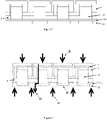
- Figure 8 illustrates a demonstration of conductive path 40 and mechanical load transmission 35.
- the conductive path 40 is formed through the semiconductor chip 2, conductive block 12, the diaphragm 11 and the stand-off plate 10.
- the sub-assembly is operated by clamping the whole device to a specified load 35.
- the specified load is about 50 to 70kN.
- This mechanical load 35 forces the conductive blocks 12 into the conductive diaphragm 11, causing it to deflect locally within the voids 45 in the standoff plate 10, as shown in figure 8 .
- the deflection-load characteristics are designed so that the force on each individual chip 2 is approximately equal.
- Figure 9 illustrates an alternative semiconductor sub-assembly including a deflection limiting frame 13 according to one embodiment of the invention.
- the other features of Figure 9 are the same as those of Figure 8 and therefore carry the same reference numbers.
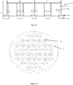
- Figure 10 illustrates a representation of a stand-off plate 10 including through holes or voids 45.
- the conductive diaphragm 11 is generally flexed through each hole or void 45 of the stand-off plate 10.
- One embodiment of the invention uses the stress strain relationship of the conductive diaphragm 11.
- the material for the diaphragm may possess a high yield strength to limit the amount of plastic deformation to a tolerable level and maintain this behaviour at elevated temperatures (e.g. 125°C).
- a suitable material would be stainless steel (e.g. X10 Cr Ni 18-8).
- Figure 11 illustrates the different capabilities of the traditional construction (line A) and one embodiment of the invention (line B) to compensate for differences in thicknesses of the components (particularly the diaphragm) in the semiconductor unit.
- Figure 11 illustrates the comparison using the sub-assembly of Figure 7 . It shows that when subjected to a given stress, a greater strain is achieved for one embodiment of the invention. This means that a larger variation in the thicknesses of the components (particularly the diaphragm) in the semiconductor unit can be tolerated.
- the graph assumes the materials used do not exceed their yield strength (i.e. the material is only elastically deformed).
- Figure 12 illustrates how a material typically reacts when its yield strength ( ⁇ y ) is exceeded (i.e. the material is plastically deformed).
- the material e.g. the diaphragm material
- the material reacts as for the elastic scenario in the first graph.
- the material is stressed beyond its yield strength (2), it begins to plastically deform until the maximum applied stress is reached (3).
- the stress is removed (4), the strain will decrease to a value that is equal to zero plus the amount of plastic deformation ( ⁇ post ).
- This relationship is used in conjunction with that in the first graph to enable an embodiment of the invention to tolerate even greater differences in the thicknesses of the components in the semiconductor units.
- the specified load for the finished device may be determined by the load required for optimum pressure contact to the semiconductor chip. This is determined by balancing electrical and thermal conductivity of the pressure contact with the long-term reliability. In general, a higher force will result in better conductivity, but a shorter lifetime, whereas a lower force will result in poor conductivity and longer lifetime.
- the skilled person would appreciate that so far only a mechanical prototype has been produced. These will require whole device clamping forces that differ from the about 50-70kN specified for the prototype.
- the device may have a ⁇ 225mm electrode, but different sizes are possible. The smallest device may have a ⁇ 47mm electrode.
- the device may be circular or may be square, although other shapes are possible.
- the diaphragm 11 thickness may be in the range of 0.1mm to 10mm.
- the diaphragm 11 may be made of spring steel, copper, aluminium, silver or an alloy of these materials.
- the front side 4 and backside 5 strain buffers may or may not be attached to the semiconductor chip 2 by soldering or silver sintering.
- the conductive block 12 and the frontside strain buffer 4 may be formed of one piece of material. This may or may not be attached to the frontside of the semiconductor chip 2 by soldering or silver sintering.
- the standoff plate 10 and conductive diaphragm 11 may be formed of one piece of material.
- the conductive diaphragm 11 and conductive blocks 12 may be formed of one piece of material.
- the standoff plate 10, conductive diaphragm (or conductive malleable layer) 11 and conductive blocks 12 may be formed of one piece of material.
- a mechanism that limits the deflection of the diaphragm may be added, in order to control the level of pressure that is applied to the semiconductor chips. This will take the form of a frame 13 that takes up the mechanical loading once a predetermined level of deflection (determined by the load-deflection characteristics of the diaphragm) has been reached.
- the proposed sub-assembly is a unique solution to the problem of improving pressure uniformity across a press-pack IGBT device. It allows chips to be packed very densely (and so a higher overall current rating per device) which is generally very advantageous.
Landscapes
- Die Bonding (AREA)
- Cooling Or The Like Of Semiconductors Or Solid State Devices (AREA)
- Testing Of Individual Semiconductor Devices (AREA)
Description
- The present invention relates to a semiconductor device sub-assembly.
- It is advantageous for a multiple chip device to have the following features:
- The pressure distribution across each chip and between chips is uniform;
- The applied pressure should be within a defined operating range.
- In traditional designs, semiconductor chips are placed between mechanical strain buffers, such as molybdenum or tungsten, to form a semiconductor unit. These semiconductor units are then placed between two common copper electrodes. For improved performance, in terms of current handling capability and reliability, the pressure distribution across the chips within the package should be as uniform as possible. This is difficult to achieve, as micron-level differences in semiconductor unit thickness or surface flatness variations across the copper electrodes can lead to applied pressures that differ greatly between semiconductor chips and also differ from the intended target pressure. The flatness and parallelism of components, such as heatsinks in the end-users' application will also have a significant effect on this. The effect is amplified in cases where multiple devices are clamped in a single stack for series operation, due to the additive effect of all of the tolerances within the stack. The inventor has appreciated that there are applications where up to twenty such devices are clamped in a single stack.
- It is known that the performance of semiconductor chips is affected by the level of applied pressure in pressure-contact applications, such that under- or over-pressurisation can result in sub-optimal performance and poor reliability. In addition to this, the pressure that can be applied to the chips within the traditional design is not limited in any way, so they are vulnerable to both under- and over-pressurisation by the end-user.
- One approach (shown in
figure 6 ) is to use extremely tightly toleranced components (typically matched to within 1µm), to ensure component thicknesses are as closely matched as possible and to dictate that end-users provide clamp components (such as heatsinks and load spreaders) that have a much tighter flatness tolerance for multi-chip pressure contact devices than is used for traditional single chip pressure contact devices, such as large-area thyristors (e.g. typically 10µm flatness tolerance, instead of 30µm). Tight component tolerance ranges become hard to manage with large numbers of components, as is the case in large-area multi-chip pressure contact devices. Tight flatness tolerances for clamping components also become harder to achieve across a large surface area, compounding the problem. - Another approach is to use individual disc spring stacks in line with each individual semiconductor unit within the housing in order to reduce the force/displacement ratio. In this way, for a given difference in semiconductor unit thicknesses or a given flatness variation, the difference in contact pressure is minimised. As the disc springs are relatively poor electrical conductors, conductive metallic bypass strips (longitudinal current bypass) or stamped, contoured metal sheets (lateral current bypass) are used. Bypass strips run from the top to the bottom of the stack of disc springs. When the disc springs are compressed, the flexible bypass strip bows outwards. This arrangement is used in ABB's StakPak arrangement which is shown in
figure 1 . Due to the outward bow of the bypass strips, the packing density of chips may be limited, in turn limiting the current density of the finished device. - The stamped, contoured metal sheet is shaped as shown in
figure 2 and incorporated in the finished device described in patent numberCN103579165 . As with the longitudinal current bypass strip method infigure 1 , due to the shaping of the sheet, and the area required to form the sheet, the packing density of chips is limited, again limiting the current density of the finished device. - A further approach is to use a pressurised fluid to pressurise the contact components in the device. This has been detailed in patent
JP2004158489 - Two approaches for applying correct applied pressure are known. Both apply only to the design using disc springs described above.
- The first approach (as used in ABB's StakPak) uses the rigid insulative sleeve of the device housing as a travel-stop mechanism, which prevents depression of the external contact surfaces beyond a defined plane. The chips are grouped into sub-modules which contain the spring assemblies. Either four or six sub-modules are used in a finished device, each of which is individually tested before being assembled. The device specification requires the load to be sufficient to compress the external contact surfaces level with the top of the sleeve (referred to as the threshold load in this document). Beyond the threshold load, any excess load is supported by the sleeve and the load applied to the chips is then dictated by the load/displacement ratio of the spring system and increases no further, even with extra loading. The displacement is defined as the difference between the pre-load height of the spring stack and the loaded height of the spring stack, once the sleeve begins to carry the mechanical load. In this design, only the sleeve supports load above the threshold load around the perimeter of the device, with no mechanical support provided in the centre of the device.
- The second approach described in
CN103579165 uses a rigid insulative support frame inside the device housing to act as a travel stop mechanism. This acts in a similar manner to the perimeter travel stop mechanism described above. From the images given, it appears that load above the threshold load is supported in the centre of the device as well as at the edge. For this design to be tested or operated, the entire device must be fully assembled. Operation as a subassembly is not possible. - Investigations of pressure distribution using tightly toleranced components in a 125mm press-pack package have found pressure uniformity to be very poor. Similar trials involving a 125mm package may have also been found to have poor pressure distribution. Such difficulties achieving uniform clamping indicate that performance of the device as a whole is likely to be far from optimum. It has also been found that pressure distribution is greatly affected by the flatness of the clamping components that apply the mechanical load to the external pole faces of the device. Poor pressure distribution may have been seen even when using clamping components that were lapped flat and had measured flatness of around 5µm across their entire device contact area.
- Trends in patent activity over the past 25 years show a migration from rigid solutions for multi-chip pressure contact devices to solutions with enhanced compliance. These solutions include sprung solutions (ABB, Toshiba, Infineon, State Grid Corporation China) and solutions where the uniform pressure is provided by a pressurized fluid (Honda).
- The only rigid solutions for which significant information has been found are those of IXYS UK Westcode, Toshiba and Fuji Electric. The Fuji Electric devices may not appear to be manufactured any longer. Little information can be found on the Toshiba devices, although they may be still advertised and sold. Recent published literature from IXYS UK Westcode large-area press-pack IGBT devices indicates that they may have reliability issues, which are suspected to result from pressure distribution problems. These papers show that with a ΔTj of 78°C the cycles to failure for an IXYS UK Westcode multi-chip pressure contact device is approximately 6,000 cycles for multi-chip pressure contact devices of rigid construction. This may compare unfavourably with single chip pressure contact devices, for which at a ΔTj of 80°C the cycles to failure is far in excess of 100,000 cycles. Other published literature reviews have found by simulation that pressure uniformity may be grossly affected by micron-level differences in components in each chip's component stack.
- Published literature is available on ABB's sprung solution, the StakPak, including case studies of HVDC Light schemes around the world using as many as 6,000 StakPak devices per scheme. According to ABB's own literature, their sprung solution has proven to be generally reliable in HVDC Light schemes. This published literature even provides details of failure rates, which appear to be relatively low.
- It is desirable that to create high reliability multi-chip packages, a more compliant solution than that offered by the rigid copper electrodes is required.
- A mechanical prototype of the design has been produced. As its design intended, the pressure uniformity was changed relative to that achieved with the traditional design device.
-
US 5,828,564 relates to rectifier heat dissipation. The conductive device includes a metal base serving as one electrode and having a side surface portion and a seating surface portion and a metal heat dissipation member including a socket section for receiving metal base. -
US 5,874,774 relates to a semiconductor device which includes a plurality of semiconductor chips each of which has a first main electrode and a control electrode on a first main surface and a second main electrode on a second main surface, and a plurality of support plates each of which is secured to the second main surface of the corresponding semiconductor chip. -
US 4,224,663 relates to a mounting assembly for pass-pack semiconductive controlled rectifiers. -
US 5,994,773 relates to a ball grid array semiconductor package. -
US 5,990,501 relates to a multichip press-contact type semiconductor device, including a plurality of semiconductor chips, a plurality of heat buffer plates, a conductive metal sheet, and first and second press-contact electrode plates. - Aspects and preferred features are set out in the accompanying claims.
- According to one aspect of the present invention there is provided a semiconductor device sub-assembly in accordance with
claim 1. - A substantially uniform pressure distribution is achieved by flexing the malleable layer to a predetermined level. The invention presented here is a unique solution to the problem of improving pressure uniformity across a power device, e.g. a press-pack IGBT device. It greatly simplifies the assembly process. It allows chips to be packed very densely (and so a higher overall current rating per device).
- At least some of the conductive blocks are configured to flex the conductive malleable layer. The sub-assembly further comprises a stand-off plate operatively connected with an opposing surface of the conductive malleable layer compared to a surface of the conductive malleable layer to which the conductive block is coupled. The conductive block is generally in contact with a first surface of the malleable layer and the stand-off plate is coupled with a second opposing surface of the malleable layer.
- The stand-off plate comprises a plurality of holes or voids. During the operation of the sub-assembly, the conductive malleable layer is flexed into each hole of the stand-off plate by each conductive block. This flexing technique helps to provide substantially uniform pressure distribution across all the devices of the sub-assembly.
- The thickness of the conductive malleable layer is chosen such that the conductive malleable layer is at least elastically deformed. The yield strength of a material of the conductive malleable layer is chosen such that the conductive malleable layer is at least plastically deformed by the conductive block under the applied pressure.
- The conductive malleable layer may be at least plastically deformed at an elevated temperature between -50°c and 150°C.
- The conductive malleable layer may be a flat diaphragm. The conductive malleable layer is a continuous layer, preferably without any contoured hole or recess into it.
- The thickness of the conductive malleable layer may be from about 0.1 mm to 10 mm.
- The conductive malleable layer may comprise a material comprising copper, stainless steel, aluminium, silver, or an alloy of copper, aluminium, stainless steel and silver. The conductive block may comprise a material comprising copper, aluminium, silver, or an alloy of copper, aluminium, and silver.
- The stand-off plate may comprise a material comprising copper, aluminium, silver, or an alloy of copper, aluminium, and silver.
- The stand-off plate, conductive malleable layer and conductive blocks may be formed using one piece of material.
- The sub-assembly may further comprise a printed circuit board on the conductive malleable layer, the printed circuit board is configured to distribute a control signal applied to a control terminal of the semiconductor unit. The printed circuit board may comprise a plurality of holes, each hole being aligned with each hole of the stand-off plate. Each conductive block may be located in each hole of the printed circuit board.
- The sub-assembly is configured such that after the pressure is applied a conductive path is established through the semiconductor unit, conductive block, conductive malleable layer, and stand-off plate.
- The semiconductor unit may comprise:
- a semiconductor chip;
- a protection layer at the edge of the semiconductor chip;
- a front side strain buffer;
- a back side strain buffer;
- a control terminal connection spring pin.
- The backside strain buffer may be a disc covering all the chips within the sub-assembly.
- The backside strain buffer may comprise any one of aluminium-graphite, molybdenum and molybdenum-copper.
- The sub-assembly may further comprise a metal layer between the semiconductor chip and the frontside and backside strain buffers
- The front side strain buffer and the back side strain buffer may be attached to the semiconductor chip by a soldering technique.
- The front side strain buffer and the back side strain buffer may be attached to the semiconductor chip by a silver sintering technique.
- The sub-assembly may have a square or circular shape.
- The sub-assembly may further comprise a deflection limiting frame between the conductive malleable layer and semiconductor unit. The deflection limiting frame may comprise polyether ether ketone (PEEK).
- According to a further aspect of the present invention, there is provided a method for manufacturing a semiconductor device sub-assembly in accordance with
claim 12. - Individual semiconductor chips can be connected in parallel within a single pressure contact housing to provide a single device containing multiple chips with a current handling capability that is ideally the sum of the capability of all the chips contained within the housing.
- The conductive malleable layer may be a flat diaphragm. The conductive malleable layer may be a continuous layer without a contoured area in the malleable layer. The conductive malleable layer may be a flexible layer. The conductive malleable layer may comprise a material comprising copper, aluminium, silver and an alloy of copper, aluminium and silver.
- The sub-assembly may further comprise a printed circuit board on the conductive malleable layer, the printed circuit board is configured to distribute a control signal applied to a control terminal of the semiconductor unit.
- The semiconductor unit may comprise:
- a semiconductor chip;
- a protection layer at the edge of the semiconductor chip;
- a front side strain buffer;
- a back side strain buffer;
- a control terminal connection spring pin.
- Some preferred embodiments of the invention will now be described by way of example only and with reference to the accompanying drawings, in which:
-
Figure 1 illustrates a disc spring stack and current bypass strips according to prior art; -
Figure 2 illustrates a stamped, contoured metal sheet according to prior art; -
Figure 3 illustrates the operation of ABB's StakPak in which a rigid insulative sleeve is included according to prior art; -
Figure 4 illustrates a three-dimensional view of a finished semiconductor unit that may be provided by an embodiment of the present invention; -
Figure 5 illustrates a schematic cross-section of the semiconductor unit ofFigure 4 ; -
Figure 6 illustrates a schematic cross-section of an assembled device of a prior art construction containing multiple semiconductor units; -
Figure 7 illustrates a schematic cross-section of a semiconductor sub-assembly according to an embodiment of the present invention; -
Figure 8 illustrates a demonstration of conductive path through a semiconductor chip (jogged arrow), the mechanical loading (arrows around the periphery) and the deflection of the conductive diaphragm, in the embodiment ofFigure 7 ; -
Figure 9 illustrates an alternative semiconductor sub-assembly including a deflection limiting frame according to one embodiment of the invention; -
Figure 10 illustrates a representation of a stand-off plate of the semiconductor sub-assembly; -
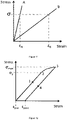
Figure 11 illustrates a comparison of the embodiment ofFigure 7 with a conventional approach with regards to stress-strain relationship of a conductive diaphragm; -
Figure 12 illustrates a demonstration of an effect of plastic deformation on the stress-strain relationship of the conductive diaphragm. - In the accompanying figures, the following components are used with reference to the following reference numerals.
- 1 - a semiconductor unit;
- 2 - a semiconductor chip, in this application is either an Insulated Gate Bipolar Transistor or Fast Recovery Diode, but other types of chips could be used;
- 3 - Moulded locator - may be a high temperature plastic including polyether ether ketone (PEEK)
- 4 - Front-side strain buffer - may comprise molybdenum, tungsten or an alloy of molybdenum and copper or tungsten and copper;
- 5 - Backside strain buffer - same as front side strain buffer;
- 6 - Control terminal connection spring pin - may be a gold-plated stainless steel;
- 7 - Device housing base/main electrode - may be copper;
- 8 - Control signal distribution printed circuit board - may be a standard high-temperature PCB material;
- 9 - Device housing lid/main electrode - may be copper;
- 10 - Standoff plate - may be copper, but may be any suitably conductive metal, such as aluminium, silver, or an alloy of these;
- 11 - Conductive diaphragm or conductive malleable layer - may be copper, but may be any suitable conductive metal, such as spring steel, aluminium or silver, or an alloy of these;
- 12 - Conductive block - may be copper, but may be any suitably conductive metal, such as aluminium, silver, or an alloy of these;
- 13 - Deflection limiting frame - may be a high temperature plastic.
-
Figure 4 illustrates a three-dimensional view of a finished semiconductor unit that may incorporate a sub-assembly in accordance with teone embodiment of the present invention. -
Figure 5 illustrates a schematic cross-section of the semiconductor unit ofFigure 4 . In one embodiment, the semiconductor unit includes asemiconductor chip 2, for example, an insulated gate bipolar transistor (IGBT), metal oxide semiconductor field effect transistor (MOSFET), bipolar junction transistor (BJT) or any other type of semiconductor devices. The unit includes afrontside strain buffer 4 and abackside strain buffer 5. Theunit 1 also includes a control terminalconnection spring pin 6. Theunit 1 also includes a mouldedlocator 3 that serves to locate thefrontside strain buffer 4,backside strain buffer 5 and control terminalconnection spring pin 6 relative to thesemiconductor chip 2. - In one embodiment, the
backside strain buffer 5 may not be an individual component for each chip, but may be one large disc of this material that covers all of the chips in the device. The frontside and backside strain buffer material may also be aluminium-graphite, as well as one of the materials already listed above. - In one embodiment, the lip on the semiconductor unit moulded
locator 3 that locates thebackside strain buffer 5 may be removed. With this lip removed, the backside strain buffers will be free to move out of alignment laterally, so a method to hold them in place will be required. In the case that an individual backside strain buffer is used for each semiconductor unit and is not bonded to the chip, this would be a plastic grid with square holes that is fixed to the semiconductor unit locator over which a thin cover of aluminium or copper is fixed to prevent the backside strain buffers from falling out of the grid if the device is turned upside down. If the backside strain buffer design is either individual squares bonded to the chip or is made using one large disc, such a locator and cover, will not be needed. - An intermediate soft metal layer may be included between the chip and the frontside and backside strain buffers. This intermediate layer may be a soft metal, such as aluminium, copper, silver, indium or a tin-silver solder preform.
- The control terminal
connection spring pin 6 may not be held by the semiconductor unit, but instead may be mounted in a separate plastic part between the semiconductor unit and the PCB. This would take the form of a thin sheet with holes drilled in the required places, which is laid onto the PCB. This separate plastic part will be located laterally by the semiconductor unit locator. -
Figure 7 illustrates a schematic cross-section of a semiconductor sub-assembly according to one embodiment of the present invention. The sub-assembly includes thesemiconductor units 1 laterally spaced from one another. Eachsemiconductor unit 1 is coupled (or operatively connected) with aconductive block 12. There is provided aconductive diaphragm 11 which is coupled with eachconductive block 12. Theconductive block 12 touches a first surface of theconductive diaphragm 11. The sub-assembly also includes a stand-off plate 10 operatively coupled or connected to a second surface of theconductive diaphragm 11. The second surface of thediaphragm 11 is an opposing surface of the first surface of theconductive diaphragm 11. In other words, theconductive diaphragm 11 is located in between the stand-off plate 10 andconductive block 12. Similarly, theconductive block 12 is located between thesemiconductor units 1 and theconductive diaphragm 11. The stand-off plate 10 includes a plurality of holes, each of which is substantially aligned with eachconductive block 12. Therefore when a mechanical load is applied to the sub-assembly, eachconductive block 12 forces theconductive diaphragm 11 to flex into each hole of the stand-off plate 10. The sub-assembly also includes a printedcircuit board 8 coupled with theconductive diaphragm 11 and thesemiconductor unit 1. The printedcircuit board 8 includes a plurality of holes each are aligned with each hole of the stand-off plate 10. - Broadly speaking, the technical aspects of the embodiment of
Figure 7 are as follows: - 1. The sub-assembly uses a flat,
conductive diaphragm 11 andstandoff plate 10 as a spring mechanism to provide improved pressure uniformity compared to the traditional construction shown infigure 6 . This approach simplifies the assembly process greatly when compared to design approaches using large numbers of disc springs. - 2. The sub-assembly uses a flat,
conductive diaphragm 11 andstandoff plate 10 to provide the current bypass path. The use of this approach wastes minimal contact area, compared to the longitudinal bypass strips that bow laterally or the stamped, contoured metal sheet that requires area to accommodate the formed contours and so permits the maximum chip packing density and therefore the maximum current density for the finished device of all current bypass methods available. - 3. The design may be a fully-functional sub-assembly. It does not use a final outer packaging - typically a ceramic housing - for testing to be carried out. Other designs encountered do require final assembly to be fully functional. Since large-area ceramic housings are expensive components and failure of the device results in irreparable damage to the contact surfaces within the ceramic housing, a cost-saving can be recognised by testing the sub-assembly before packaging, since some manufacturing yield loss is to be expected.
- 4. One embodiment of the invention uses the deflection of a single diaphragm, rather than the deflection of multiple disc springs stacked in series. This means the sub-assembly can be made much thinner than a sub-assembly using disc springs, which may offer benefits such as space-saving and weight-saving.
- In the embodiment of
Figure 8 , theconductive diaphragm 11 is placed onto thestandoff plate 10. Theconductive diaphragm 11 has a thickness specified to provide the desired spring characteristics and sufficient to carry the required current. Onto theconductive diaphragm 11 is placed a control signal distribution printedcircuit board 8. This distributes the control signal applied to the single control terminal of the finished device to each of theindividual semiconductor chips 2 within the device. Into holes in the control signal distribution printedcircuit board 8 are placedconductive blocks 12. Onto each of these is placed asemiconductor unit 1. Thesemiconductor unit 1 comprises asemiconductor chip 2 with protection from electrical breakdown at the edge of thechip 3, frontside 4 andbackside 5 strain buffers and a control terminal connection spring pin 6 (only for chips with a control terminal). - The sub-assembly may subsequently be assembled into a traditional ceramic capsule or other appropriate power semiconductor housing (not shown).
-
Figure 8 illustrates a demonstration ofconductive path 40 andmechanical load transmission 35. Theconductive path 40 is formed through thesemiconductor chip 2,conductive block 12, thediaphragm 11 and the stand-off plate 10. In one embodiment, the sub-assembly is operated by clamping the whole device to a specifiedload 35. In one example the specified load is about 50 to 70kN. Thismechanical load 35 forces theconductive blocks 12 into theconductive diaphragm 11, causing it to deflect locally within thevoids 45 in thestandoff plate 10, as shown infigure 8 . The deflection-load characteristics are designed so that the force on eachindividual chip 2 is approximately equal. -
Figure 9 illustrates an alternative semiconductor sub-assembly including adeflection limiting frame 13 according to one embodiment of the invention. The other features ofFigure 9 are the same as those ofFigure 8 and therefore carry the same reference numbers. -
Figure 10 illustrates a representation of a stand-off plate 10 including through holes or voids 45. Theconductive diaphragm 11 is generally flexed through each hole or void 45 of the stand-off plate 10. - One embodiment of the invention uses the stress strain relationship of the
conductive diaphragm 11. The material for the diaphragm may possess a high yield strength to limit the amount of plastic deformation to a tolerable level and maintain this behaviour at elevated temperatures (e.g. 125°C). A suitable material would be stainless steel (e.g. X10 Cr Ni 18-8).Figure 11 illustrates the different capabilities of the traditional construction (line A) and one embodiment of the invention (line B) to compensate for differences in thicknesses of the components (particularly the diaphragm) in the semiconductor unit.Figure 11 illustrates the comparison using the sub-assembly ofFigure 7 . It shows that when subjected to a given stress, a greater strain is achieved for one embodiment of the invention. This means that a larger variation in the thicknesses of the components (particularly the diaphragm) in the semiconductor unit can be tolerated. The graph assumes the materials used do not exceed their yield strength (i.e. the material is only elastically deformed). -
Figure 12 illustrates how a material typically reacts when its yield strength (σy) is exceeded (i.e. the material is plastically deformed). Initially (1), the material (e.g. the diaphragm material) reacts as for the elastic scenario in the first graph. When the material is stressed beyond its yield strength (2), it begins to plastically deform until the maximum applied stress is reached (3). At this point, if the stress is removed (4), the strain will decrease to a value that is equal to zero plus the amount of plastic deformation (εpost). This relationship is used in conjunction with that in the first graph to enable an embodiment of the invention to tolerate even greater differences in the thicknesses of the components in the semiconductor units. - It will be appreciated that the specified load for the finished device may be determined by the load required for optimum pressure contact to the semiconductor chip. This is determined by balancing electrical and thermal conductivity of the pressure contact with the long-term reliability. In general, a higher force will result in better conductivity, but a shorter lifetime, whereas a lower force will result in poor conductivity and longer lifetime.
- The skilled person would appreciate that so far only a mechanical prototype has been produced. These will require whole device clamping forces that differ from the about 50-70kN specified for the prototype. The device may have a ~225mm electrode, but different sizes are possible. The smallest device may have a ∼47mm electrode.
- Finished devices of different diameters may be manufactured as necessary. The device may be circular or may be square, although other shapes are possible. The
diaphragm 11 thickness may be in the range of 0.1mm to 10mm. Thediaphragm 11 may be made of spring steel, copper, aluminium, silver or an alloy of these materials. - The
front side 4 andbackside 5 strain buffers may or may not be attached to thesemiconductor chip 2 by soldering or silver sintering. - The
conductive block 12 and thefrontside strain buffer 4 may be formed of one piece of material. This may or may not be attached to the frontside of thesemiconductor chip 2 by soldering or silver sintering. - The
standoff plate 10 andconductive diaphragm 11 may be formed of one piece of material. Theconductive diaphragm 11 andconductive blocks 12 may be formed of one piece of material. Thestandoff plate 10, conductive diaphragm (or conductive malleable layer) 11 andconductive blocks 12 may be formed of one piece of material. - In one embodiment, a mechanism that limits the deflection of the diaphragm may be added, in order to control the level of pressure that is applied to the semiconductor chips. This will take the form of a
frame 13 that takes up the mechanical loading once a predetermined level of deflection (determined by the load-deflection characteristics of the diaphragm) has been reached. - The proposed sub-assembly is a unique solution to the problem of improving pressure uniformity across a press-pack IGBT device. It allows chips to be packed very densely (and so a higher overall current rating per device) which is generally very advantageous.
- Although the above mentioned description is directed to a power semiconductor device chip but it would be appreciated that other semiconductor devices could also be possible to use in this invention.
- The skilled person will understand that in the preceding description and appended claims, positional terms such as 'above', 'overlap', 'under', 'lateral', etc. are made with reference to conceptual illustrations of an device, such as those showing standard cross-sectional perspectives and those shown in the appended drawings. These terms are used for ease of reference but are not intended to be of limiting nature. These terms are therefore to be understood as referring to a device when in an orientation as shown in the accompanying drawings.
- Although the invention has been described in terms of preferred embodiments as set forth above, it should be understood that these embodiments are illustrative only and that the claims are not limited to those embodiments. Those skilled in the art will be able to make modifications and alternatives in view of the disclosure which are contemplated as falling within the scope of the appended claims.
Claims (12)
- A semiconductor device sub-assembly comprising:a plurality of semiconductor units (1) laterally spaced to one another;a plurality of conductive blocks (12) operatively coupled with the plurality of semiconductor units (1);a conductive malleable layer (11) operatively coupled with the plurality of conductive blocks (12), wherein the conductive malleable layer (11) is a continuous layer, and wherein the plurality of conductive blocks (12) are located between the conductive malleable layer (11) and the plurality of semiconductor units (1);a conductive stand-off plate (10) operatively connected with an opposing surface of the conductive malleable layer (11) compared to a surface of the conductive malleable layer (11) to which the conductive block (12) is coupled, wherein the stand-off plate (10) comprises a plurality of holes, each of which is substantially aligned with a corresponding conductive block (12); andmeans for applying a mechanical load to the sub-assembly;wherein, in use, the plurality of conductive blocks (12) apply a pressure on the conductive malleable layer (11), when a predetermined pressure is applied by the mechanical means to the semiconductor units (1) and the stand-off plate (10) of the semiconductor device sub-assembly such that the conductive malleable layer (11) is flexed into the holes of the stand-off plate (10) by the plurality of conductive blocks (12), andwherein the sub-assembly is configured such that when the predetermined pressure is applied a conductive path is established through the semiconductor unit (1), conductive block (12), conductive malleable layer (11), and stand-off plate (10).
- A sub-assembly according to claim 1 wherein a yield strength of a material of the conductive malleable layer (11) is chosen such that the conductive malleable layer (11) is at least plastically deformed by the conductive block (12) under the applied pressure; and optionally
wherein the conductive malleable layer (11) is at least plastically deformed at a temperature between -50°c and 150°C. - A sub-assembly according to any preceding claim, wherein the conductive malleable layer (11) is a flat diaphragm; and/orwherein the thickness of the conductive malleable layer (11) is from about 0.1 mm to 10mm; and/orwherein the conductive malleable layer (11) comprises a material comprising copper, stainless steel, aluminium, silver, or an alloy of copper, aluminium, stainless steel and silver; and/orwherein the conductive block (12) comprises a material comprising copper, aluminium, silver, or an alloy of copper, aluminium, and silver.
- A sub-assembly according to any preceding claim, wherein the stand-off plate (10) comprises a material comprising copper, aluminium, silver, or an alloy of copper, aluminium, and silver.
- A sub-assembly according to any preceding claim, wherein the conductive malleable layer (11) and conductive blocks (12) are formed using one piece of material.
- A sub-assembly according to any one of claims 1 to 4, wherein the stand-off plate (10) and conductive malleable layer (11) are formed using one piece of material; or
wherein the stand-off plate (10), conductive malleable layer (11) and conductive blocks (12) are formed using one piece of material. - A sub-assembly according to any preceding claim, further comprising a deflection limiting frame (13) between the conductive malleable layer (11) and semiconductor unit (1), and wherein the deflection limiting frame (13) comprises polyether ether ketone.
- A sub-assembly according to any preceding claim, wherein the semiconductor unit (1) comprises:a semiconductor chip (2);a protection layer (3) at the edge of the semiconductor chip;a front side strain buffer (4);a back side strain buffer (5);a control terminal connection spring pin (6).
- A sub-assembly according to claim 8, wherein the backside strain buffer (5) is a disc covering all the chips (1) within the sub-assembly; and optionallywherein the backside strain buffer (5) comprises any one of aluminium-graphite, molybdenum and molybdenum-copper; and/orfurther comprising a metal layer between the semiconductor chip (1) and the frontside and backside strain buffers (4, 5).
- A sub-assembly according to claim 8 or 9, wherein the front side strain buffer (4) and the back side strain buffer (5) are attached to the semiconductor chip (1) by solder; or
wherein the front side strain buffer (4) and the back side strain buffer (5) are attached to the semiconductor chip (1) by sintered silver. - A sub-assembly according to any preceding claim, wherein the sub-assembly has a square or circular shape.
- A method for manufacturing a semiconductor device sub-assembly, the method comprising:providing a plurality of semiconductor units (1) laterally spaced to one another;providing a plurality of conductive blocks (12) operatively coupled with the plurality of semiconductor units (1);providing a conductive malleable layer (11) operatively coupled with the plurality of conductive blocks (12), wherein the conductive malleable layer (11) is a continuous layer, and wherein the plurality of conductive blocks (12) are located between the conductive malleable layer (11) and the plurality of semiconductor units (1);providing a conductive stand-off plate (10) operatively connected with an opposing surface of the conductive malleable layer (11) compared to a surface of the conductive malleable layer (11) to which the conductive block (12) is coupled, wherein the stand-off plate (10) comprises a plurality of holes, each of which is substantially aligned with a corresponding conductive block; andproviding means for applying a mechanical load to the sub-assembly such thatin use, the plurality of conductive blocks (12) apply a pressure on the conductive malleable layer (11), when a predetermined pressure is applied to the semiconductor units (1) and the stand-off plate (10) of the semiconductor device sub-assembly such that the conductive malleable layer (11) is flexed into the holes of the stand-off plate (10) by the plurality of conductive blocks (12), and
wherein the sub-assembly is configured such that when the predetermined pressure is applied a conductive path is established through the semiconductor unit (1), conductive block (12), conductive malleable layer (11), and stand-off plate (10).
Applications Claiming Priority (2)
| Application Number | Priority Date | Filing Date | Title |
|---|---|---|---|
| PCT/GB2016/051842 WO2017220949A1 (en) | 2016-06-20 | 2016-06-20 | A semiconductor device sub-assembly |
| PCT/GB2017/050169 WO2017220955A1 (en) | 2016-06-20 | 2017-01-23 | Semiconductor device sub-assembly |
Publications (2)
| Publication Number | Publication Date |
|---|---|
| EP3472864A1 EP3472864A1 (en) | 2019-04-24 |
| EP3472864B1 true EP3472864B1 (en) | 2022-11-09 |
Family
ID=56263985
Family Applications (2)
| Application Number | Title | Priority Date | Filing Date |
|---|---|---|---|
| EP16732697.4A Active EP3472860B1 (en) | 2016-06-20 | 2016-06-20 | A semiconductor device sub-assembly |
| EP17701919.7A Active EP3472864B1 (en) | 2016-06-20 | 2017-01-23 | Semiconductor device sub-assembly and manufacturing method thereof |
Family Applications Before (1)
| Application Number | Title | Priority Date | Filing Date |
|---|---|---|---|
| EP16732697.4A Active EP3472860B1 (en) | 2016-06-20 | 2016-06-20 | A semiconductor device sub-assembly |
Country Status (4)
| Country | Link |
|---|---|
| US (2) | US11195784B2 (en) |
| EP (2) | EP3472860B1 (en) |
| CN (2) | CN108701667B (en) |
| WO (2) | WO2017220949A1 (en) |
Families Citing this family (11)
| Publication number | Priority date | Publication date | Assignee | Title |
|---|---|---|---|---|
| WO2020012143A1 (en) | 2018-07-11 | 2020-01-16 | Dynex Semiconductor Limited | Semiconductor device sub-assembly |
| CN112992795B (en) * | 2019-12-17 | 2024-04-19 | 株洲中车时代半导体有限公司 | Crimping type IGBT sub-module structure and crimping type IGBT device |
| CN112992866A (en) * | 2019-12-18 | 2021-06-18 | 株洲中车时代半导体有限公司 | Current bypass structure and IGBT device |
| CN113053831B (en) * | 2019-12-27 | 2023-09-05 | 株洲中车时代半导体有限公司 | A crimping type IGBT module and power semiconductor device |
| CN111952322B (en) * | 2020-08-14 | 2022-06-03 | 电子科技大学 | Flexible semiconductor film with periodically adjustable buckling structure and preparation method thereof |
| CN112636054B (en) | 2020-11-27 | 2022-08-05 | 株洲中车时代半导体有限公司 | Semiconductor device assembly, pressure-contact power semiconductor module and manufacturing method |
| CN112712920A (en) * | 2020-12-22 | 2021-04-27 | 欧耐特线缆集团有限公司 | Fireproof cable of ageing resistance |
| CN113013147B (en) * | 2021-04-16 | 2024-12-06 | 南瑞联研半导体有限责任公司 | A semiconductor module |
| WO2022248068A1 (en) | 2021-05-28 | 2022-12-01 | Dynex Semiconductor Limited | Semiconductor device |
| US20240213106A1 (en) | 2021-07-19 | 2024-06-27 | Dynex Semiconductor Limited | Semiconductor device |
| US12506044B2 (en) | 2021-07-19 | 2025-12-23 | Dynex Semiconductor Limited | Semiconductor device |
Citations (1)
| Publication number | Priority date | Publication date | Assignee | Title |
|---|---|---|---|---|
| US5990501A (en) * | 1996-05-31 | 1999-11-23 | Kabushiki Kaisha Toshiba | Multichip press-contact type semiconductor device |
Family Cites Families (26)
| Publication number | Priority date | Publication date | Assignee | Title |
|---|---|---|---|---|
| DE2728313A1 (en) * | 1977-06-23 | 1979-01-04 | Siemens Ag | SEMICONDUCTOR COMPONENT |
| US4224663A (en) * | 1979-02-01 | 1980-09-23 | Power Control Corporation | Mounting assembly for semiconductive controlled rectifiers |
| JPS57196535A (en) | 1981-05-28 | 1982-12-02 | Toshiba Corp | Semiconductor device for electric power |
| DE3143336A1 (en) * | 1981-10-31 | 1983-05-19 | SEMIKRON Gesellschaft für Gleichrichterbau u. Elektronik mbH, 8500 Nürnberg | SEMICONDUCTOR RECTIFIER UNIT |
| JPH081914B2 (en) * | 1987-03-31 | 1996-01-10 | 株式会社東芝 | Pressure contact type semiconductor device |
| JP3588503B2 (en) * | 1995-06-20 | 2004-11-10 | 株式会社東芝 | Pressure welding type semiconductor device |
| JP3018971B2 (en) * | 1995-12-18 | 2000-03-13 | 富士電機株式会社 | Semiconductor device |
| JP3080579B2 (en) * | 1996-03-06 | 2000-08-28 | 富士機工電子株式会社 | Manufacturing method of air rear grid array package |
| JP3426101B2 (en) * | 1997-02-25 | 2003-07-14 | 三菱電機株式会社 | Rectifier |
| KR100214560B1 (en) * | 1997-03-05 | 1999-08-02 | 구본준 | Semiconductor Multichip Module |
| JP2930074B1 (en) * | 1998-06-02 | 1999-08-03 | 富士電機株式会社 | Semiconductor device |
| US6058014A (en) * | 1998-10-13 | 2000-05-02 | International Business Machines Corporation | Enhanced mounting hardware for a circuit board |
| DE19903245A1 (en) * | 1999-01-27 | 2000-08-03 | Asea Brown Boveri | Power semiconductor module |
| JP2001036002A (en) * | 1999-07-23 | 2001-02-09 | Fuji Electric Co Ltd | Semiconductor device |
| JP2004158489A (en) | 2002-11-01 | 2004-06-03 | Honda Motor Co Ltd | Pressure contact type semiconductor device |
| US6678163B1 (en) * | 2002-12-19 | 2004-01-13 | Westcode Semiconductors Limited | Housing for semiconductor chips |
| DE102005024900B4 (en) * | 2004-06-08 | 2012-08-16 | Fuji Electric Co., Ltd. | power module |
| US8531027B2 (en) * | 2010-04-30 | 2013-09-10 | General Electric Company | Press-pack module with power overlay interconnection |
| CN201708683U (en) | 2010-05-29 | 2011-01-12 | 比亚迪股份有限公司 | Intelligent crimping power module |
| US9076752B2 (en) * | 2012-02-14 | 2015-07-07 | Panasonic Intellectual Property Management Co., Ltd. | Semiconductor device and method for manufacturing the same |
| FR2994333B1 (en) * | 2012-08-03 | 2014-08-01 | Ge Energy Power Conversion Technology Ltd | SEMICONDUCTOR ELECTRONIC DEVICE FOR MOUNTING IN A PRESSED STACK ASSEMBLY AND PRESSED STACK ASSEMBLY COMPRISING SUCH A DEVICE |
| KR102170192B1 (en) * | 2013-08-22 | 2020-10-26 | 삼성전자주식회사 | Bonding apparatus , bonding method, and method for manufacturing substrates |
| US9177943B2 (en) * | 2013-10-15 | 2015-11-03 | Ixys Corporation | Power device cassette with auxiliary emitter contact |
| CN103579165B (en) | 2013-11-04 | 2016-08-31 | 国家电网公司 | A kind of Full-pressure-weldinpower power device |
| JP2016062983A (en) | 2014-09-16 | 2016-04-25 | 株式会社東芝 | Semiconductor device |
| CN104966704B (en) | 2015-07-23 | 2019-01-25 | 国网智能电网研究院 | A low thermal resistance press-fit power device package |
-
2016
- 2016-06-20 CN CN201680006071.XA patent/CN108701667B/en active Active
- 2016-06-20 WO PCT/GB2016/051842 patent/WO2017220949A1/en not_active Ceased
- 2016-06-20 EP EP16732697.4A patent/EP3472860B1/en active Active
- 2016-06-20 US US16/311,780 patent/US11195784B2/en active Active
-
2017
- 2017-01-23 WO PCT/GB2017/050169 patent/WO2017220955A1/en not_active Ceased
- 2017-01-23 EP EP17701919.7A patent/EP3472864B1/en active Active
- 2017-01-23 US US16/311,833 patent/US10777494B2/en active Active
- 2017-01-23 CN CN201780000603.3A patent/CN107851643B/en active Active
Patent Citations (1)
| Publication number | Priority date | Publication date | Assignee | Title |
|---|---|---|---|---|
| US5990501A (en) * | 1996-05-31 | 1999-11-23 | Kabushiki Kaisha Toshiba | Multichip press-contact type semiconductor device |
Also Published As
| Publication number | Publication date |
|---|---|
| WO2017220949A1 (en) | 2017-12-28 |
| WO2017220955A1 (en) | 2017-12-28 |
| CN108701667A (en) | 2018-10-23 |
| US10777494B2 (en) | 2020-09-15 |
| US20190259693A1 (en) | 2019-08-22 |
| EP3472864A1 (en) | 2019-04-24 |
| CN107851643A (en) | 2018-03-27 |
| EP3472860B1 (en) | 2022-08-17 |
| CN108701667B (en) | 2020-08-28 |
| EP3472860A1 (en) | 2019-04-24 |
| US20190206776A1 (en) | 2019-07-04 |
| US11195784B2 (en) | 2021-12-07 |
| CN107851643B (en) | 2020-08-28 |
Similar Documents
| Publication | Publication Date | Title |
|---|---|---|
| US10777494B2 (en) | Semiconductor device sub-assembly | |
| US5654877A (en) | Lead-on-chip integrated circuit apparatus | |
| US5221642A (en) | Lead-on-chip integrated circuit fabrication method | |
| US6459582B1 (en) | Heatsink apparatus for de-coupling clamping forces on an integrated circuit package | |
| EP0245179B1 (en) | System for detachably mounting semiconductors on conductor substrate. | |
| US20190259711A1 (en) | Semiconductor device and method for manufacturing the same and wireless communication apparatus | |
| JP2014510413A (en) | Connection support for semiconductor chip and semiconductor element | |
| CN114207817A (en) | Power semiconductor device | |
| US20240213106A1 (en) | Semiconductor device | |
| EP0473260A1 (en) | Fabrication of semiconductor packages | |
| US11574894B2 (en) | Semiconductor device sub-assembly | |
| JP2017135012A (en) | Method for manufacturing power storage device module | |
| TWI254429B (en) | Flexible flip chip package structure | |
| US7285852B2 (en) | Semiconductor device capsule | |
| JP6452748B2 (en) | Method for manufacturing laminated member | |
| JP7734202B2 (en) | Chip Package | |
| JP7460862B2 (en) | POWER SEMICONDUCTOR MODULE, POWER SEMICONDUCTOR ASSEMBLY, AND METHOD FOR MANUFACTURING POWER SEMICONDUCTOR MODULE | |
| KR102701220B1 (en) | Method of manufacturing silicon particles | |
| JPS6074461A (en) | Semiconductor device | |
| JP2025119881A (en) | electronic equipment | |
| JP2017188622A (en) | Semiconductor device |
Legal Events
| Date | Code | Title | Description |
|---|---|---|---|
| STAA | Information on the status of an ep patent application or granted ep patent |
Free format text: STATUS: UNKNOWN |
|
| STAA | Information on the status of an ep patent application or granted ep patent |
Free format text: STATUS: THE INTERNATIONAL PUBLICATION HAS BEEN MADE |
|
| PUAI | Public reference made under article 153(3) epc to a published international application that has entered the european phase |
Free format text: ORIGINAL CODE: 0009012 |
|
| STAA | Information on the status of an ep patent application or granted ep patent |
Free format text: STATUS: REQUEST FOR EXAMINATION WAS MADE |
|
| 17P | Request for examination filed |
Effective date: 20181227 |
|
| AK | Designated contracting states |
Kind code of ref document: A1 Designated state(s): AL AT BE BG CH CY CZ DE DK EE ES FI FR GB GR HR HU IE IS IT LI LT LU LV MC MK MT NL NO PL PT RO RS SE SI SK SM TR |
|
| AX | Request for extension of the european patent |
Extension state: BA ME |
|
| DAV | Request for validation of the european patent (deleted) | ||
| DAX | Request for extension of the european patent (deleted) | ||
| STAA | Information on the status of an ep patent application or granted ep patent |
Free format text: STATUS: EXAMINATION IS IN PROGRESS |
|
| 17Q | First examination report despatched |
Effective date: 20200220 |
|
| REG | Reference to a national code |
Ref country code: DE Ref legal event code: R079 Ref document number: 602017063495 Country of ref document: DE Free format text: PREVIOUS MAIN CLASS: H01L0025110000 Ipc: H01L0025070000 |
|
| RIC1 | Information provided on ipc code assigned before grant |
Ipc: H01L 25/11 20060101ALI20220407BHEP Ipc: H01L 23/498 20060101ALI20220407BHEP Ipc: H01L 23/051 20060101ALI20220407BHEP Ipc: H01L 25/07 20060101AFI20220407BHEP |
|
| GRAP | Despatch of communication of intention to grant a patent |
Free format text: ORIGINAL CODE: EPIDOSNIGR1 |
|
| STAA | Information on the status of an ep patent application or granted ep patent |
Free format text: STATUS: GRANT OF PATENT IS INTENDED |
|
| INTG | Intention to grant announced |
Effective date: 20220525 |
|
| GRAS | Grant fee paid |
Free format text: ORIGINAL CODE: EPIDOSNIGR3 |
|
| GRAA | (expected) grant |
Free format text: ORIGINAL CODE: 0009210 |
|
| STAA | Information on the status of an ep patent application or granted ep patent |
Free format text: STATUS: THE PATENT HAS BEEN GRANTED |
|
| AK | Designated contracting states |
Kind code of ref document: B1 Designated state(s): AL AT BE BG CH CY CZ DE DK EE ES FI FR GB GR HR HU IE IS IT LI LT LU LV MC MK MT NL NO PL PT RO RS SE SI SK SM TR |
|
| REG | Reference to a national code |
Ref country code: GB Ref legal event code: FG4D |
|
| REG | Reference to a national code |
Ref country code: CH Ref legal event code: EP Ref country code: AT Ref legal event code: REF Ref document number: 1530936 Country of ref document: AT Kind code of ref document: T Effective date: 20221115 |
|
| REG | Reference to a national code |
Ref country code: DE Ref legal event code: R096 Ref document number: 602017063495 Country of ref document: DE |
|
| REG | Reference to a national code |
Ref country code: IE Ref legal event code: FG4D |
|
| REG | Reference to a national code |
Ref country code: LT Ref legal event code: MG9D |
|
| REG | Reference to a national code |
Ref country code: NL Ref legal event code: MP Effective date: 20221109 |
|
| REG | Reference to a national code |
Ref country code: AT Ref legal event code: MK05 Ref document number: 1530936 Country of ref document: AT Kind code of ref document: T Effective date: 20221109 |
|
| PG25 | Lapsed in a contracting state [announced via postgrant information from national office to epo] |
Ref country code: SE Free format text: LAPSE BECAUSE OF FAILURE TO SUBMIT A TRANSLATION OF THE DESCRIPTION OR TO PAY THE FEE WITHIN THE PRESCRIBED TIME-LIMIT Effective date: 20221109 Ref country code: PT Free format text: LAPSE BECAUSE OF FAILURE TO SUBMIT A TRANSLATION OF THE DESCRIPTION OR TO PAY THE FEE WITHIN THE PRESCRIBED TIME-LIMIT Effective date: 20230309 Ref country code: NO Free format text: LAPSE BECAUSE OF FAILURE TO SUBMIT A TRANSLATION OF THE DESCRIPTION OR TO PAY THE FEE WITHIN THE PRESCRIBED TIME-LIMIT Effective date: 20230209 Ref country code: LT Free format text: LAPSE BECAUSE OF FAILURE TO SUBMIT A TRANSLATION OF THE DESCRIPTION OR TO PAY THE FEE WITHIN THE PRESCRIBED TIME-LIMIT Effective date: 20221109 Ref country code: FI Free format text: LAPSE BECAUSE OF FAILURE TO SUBMIT A TRANSLATION OF THE DESCRIPTION OR TO PAY THE FEE WITHIN THE PRESCRIBED TIME-LIMIT Effective date: 20221109 Ref country code: ES Free format text: LAPSE BECAUSE OF FAILURE TO SUBMIT A TRANSLATION OF THE DESCRIPTION OR TO PAY THE FEE WITHIN THE PRESCRIBED TIME-LIMIT Effective date: 20221109 Ref country code: AT Free format text: LAPSE BECAUSE OF FAILURE TO SUBMIT A TRANSLATION OF THE DESCRIPTION OR TO PAY THE FEE WITHIN THE PRESCRIBED TIME-LIMIT Effective date: 20221109 |
|
| PG25 | Lapsed in a contracting state [announced via postgrant information from national office to epo] |
Ref country code: RS Free format text: LAPSE BECAUSE OF FAILURE TO SUBMIT A TRANSLATION OF THE DESCRIPTION OR TO PAY THE FEE WITHIN THE PRESCRIBED TIME-LIMIT Effective date: 20221109 Ref country code: PL Free format text: LAPSE BECAUSE OF FAILURE TO SUBMIT A TRANSLATION OF THE DESCRIPTION OR TO PAY THE FEE WITHIN THE PRESCRIBED TIME-LIMIT Effective date: 20221109 Ref country code: LV Free format text: LAPSE BECAUSE OF FAILURE TO SUBMIT A TRANSLATION OF THE DESCRIPTION OR TO PAY THE FEE WITHIN THE PRESCRIBED TIME-LIMIT Effective date: 20221109 Ref country code: IS Free format text: LAPSE BECAUSE OF FAILURE TO SUBMIT A TRANSLATION OF THE DESCRIPTION OR TO PAY THE FEE WITHIN THE PRESCRIBED TIME-LIMIT Effective date: 20230309 Ref country code: HR Free format text: LAPSE BECAUSE OF FAILURE TO SUBMIT A TRANSLATION OF THE DESCRIPTION OR TO PAY THE FEE WITHIN THE PRESCRIBED TIME-LIMIT Effective date: 20221109 Ref country code: GR Free format text: LAPSE BECAUSE OF FAILURE TO SUBMIT A TRANSLATION OF THE DESCRIPTION OR TO PAY THE FEE WITHIN THE PRESCRIBED TIME-LIMIT Effective date: 20230210 |
|
| PG25 | Lapsed in a contracting state [announced via postgrant information from national office to epo] |
Ref country code: NL Free format text: LAPSE BECAUSE OF FAILURE TO SUBMIT A TRANSLATION OF THE DESCRIPTION OR TO PAY THE FEE WITHIN THE PRESCRIBED TIME-LIMIT Effective date: 20221109 |
|
| P01 | Opt-out of the competence of the unified patent court (upc) registered |
Effective date: 20230528 |
|
| PG25 | Lapsed in a contracting state [announced via postgrant information from national office to epo] |
Ref country code: SM Free format text: LAPSE BECAUSE OF FAILURE TO SUBMIT A TRANSLATION OF THE DESCRIPTION OR TO PAY THE FEE WITHIN THE PRESCRIBED TIME-LIMIT Effective date: 20221109 Ref country code: RO Free format text: LAPSE BECAUSE OF FAILURE TO SUBMIT A TRANSLATION OF THE DESCRIPTION OR TO PAY THE FEE WITHIN THE PRESCRIBED TIME-LIMIT Effective date: 20221109 Ref country code: EE Free format text: LAPSE BECAUSE OF FAILURE TO SUBMIT A TRANSLATION OF THE DESCRIPTION OR TO PAY THE FEE WITHIN THE PRESCRIBED TIME-LIMIT Effective date: 20221109 Ref country code: DK Free format text: LAPSE BECAUSE OF FAILURE TO SUBMIT A TRANSLATION OF THE DESCRIPTION OR TO PAY THE FEE WITHIN THE PRESCRIBED TIME-LIMIT Effective date: 20221109 Ref country code: CZ Free format text: LAPSE BECAUSE OF FAILURE TO SUBMIT A TRANSLATION OF THE DESCRIPTION OR TO PAY THE FEE WITHIN THE PRESCRIBED TIME-LIMIT Effective date: 20221109 |
|
| REG | Reference to a national code |
Ref country code: DE Ref legal event code: R097 Ref document number: 602017063495 Country of ref document: DE |
|
| PG25 | Lapsed in a contracting state [announced via postgrant information from national office to epo] |
Ref country code: SK Free format text: LAPSE BECAUSE OF FAILURE TO SUBMIT A TRANSLATION OF THE DESCRIPTION OR TO PAY THE FEE WITHIN THE PRESCRIBED TIME-LIMIT Effective date: 20221109 Ref country code: AL Free format text: LAPSE BECAUSE OF FAILURE TO SUBMIT A TRANSLATION OF THE DESCRIPTION OR TO PAY THE FEE WITHIN THE PRESCRIBED TIME-LIMIT Effective date: 20221109 |
|
| REG | Reference to a national code |
Ref country code: CH Ref legal event code: PL |
|
| PLBE | No opposition filed within time limit |
Free format text: ORIGINAL CODE: 0009261 |
|
| STAA | Information on the status of an ep patent application or granted ep patent |
Free format text: STATUS: NO OPPOSITION FILED WITHIN TIME LIMIT |
|
| PG25 | Lapsed in a contracting state [announced via postgrant information from national office to epo] |
Ref country code: LU Free format text: LAPSE BECAUSE OF NON-PAYMENT OF DUE FEES Effective date: 20230123 |
|
| REG | Reference to a national code |
Ref country code: BE Ref legal event code: MM Effective date: 20230131 |
|
| 26N | No opposition filed |
Effective date: 20230810 |
|
| PG25 | Lapsed in a contracting state [announced via postgrant information from national office to epo] |
Ref country code: LI Free format text: LAPSE BECAUSE OF NON-PAYMENT OF DUE FEES Effective date: 20230131 Ref country code: CH Free format text: LAPSE BECAUSE OF NON-PAYMENT OF DUE FEES Effective date: 20230131 |
|
| PG25 | Lapsed in a contracting state [announced via postgrant information from national office to epo] |
Ref country code: SI Free format text: LAPSE BECAUSE OF FAILURE TO SUBMIT A TRANSLATION OF THE DESCRIPTION OR TO PAY THE FEE WITHIN THE PRESCRIBED TIME-LIMIT Effective date: 20221109 Ref country code: BE Free format text: LAPSE BECAUSE OF NON-PAYMENT OF DUE FEES Effective date: 20230131 |
|
| PG25 | Lapsed in a contracting state [announced via postgrant information from national office to epo] |
Ref country code: IE Free format text: LAPSE BECAUSE OF NON-PAYMENT OF DUE FEES Effective date: 20230123 |
|
| PG25 | Lapsed in a contracting state [announced via postgrant information from national office to epo] |
Ref country code: IT Free format text: LAPSE BECAUSE OF FAILURE TO SUBMIT A TRANSLATION OF THE DESCRIPTION OR TO PAY THE FEE WITHIN THE PRESCRIBED TIME-LIMIT Effective date: 20221109 |
|
| PG25 | Lapsed in a contracting state [announced via postgrant information from national office to epo] |
Ref country code: MC Free format text: LAPSE BECAUSE OF FAILURE TO SUBMIT A TRANSLATION OF THE DESCRIPTION OR TO PAY THE FEE WITHIN THE PRESCRIBED TIME-LIMIT Effective date: 20221109 |
|
| PG25 | Lapsed in a contracting state [announced via postgrant information from national office to epo] |
Ref country code: MC Free format text: LAPSE BECAUSE OF FAILURE TO SUBMIT A TRANSLATION OF THE DESCRIPTION OR TO PAY THE FEE WITHIN THE PRESCRIBED TIME-LIMIT Effective date: 20221109 |
|
| PG25 | Lapsed in a contracting state [announced via postgrant information from national office to epo] |
Ref country code: BG Free format text: LAPSE BECAUSE OF FAILURE TO SUBMIT A TRANSLATION OF THE DESCRIPTION OR TO PAY THE FEE WITHIN THE PRESCRIBED TIME-LIMIT Effective date: 20221109 |
|
| REG | Reference to a national code |
Ref country code: DE Ref legal event code: R079 Ref document number: 602017063495 Country of ref document: DE Free format text: PREVIOUS MAIN CLASS: H01L0025070000 Ipc: H10D0080200000 |
|
| PG25 | Lapsed in a contracting state [announced via postgrant information from national office to epo] |
Ref country code: BG Free format text: LAPSE BECAUSE OF FAILURE TO SUBMIT A TRANSLATION OF THE DESCRIPTION OR TO PAY THE FEE WITHIN THE PRESCRIBED TIME-LIMIT Effective date: 20221109 |
|
| PG25 | Lapsed in a contracting state [announced via postgrant information from national office to epo] |
Ref country code: CY Free format text: LAPSE BECAUSE OF FAILURE TO SUBMIT A TRANSLATION OF THE DESCRIPTION OR TO PAY THE FEE WITHIN THE PRESCRIBED TIME-LIMIT; INVALID AB INITIO Effective date: 20170123 |
|
| PG25 | Lapsed in a contracting state [announced via postgrant information from national office to epo] |
Ref country code: HU Free format text: LAPSE BECAUSE OF FAILURE TO SUBMIT A TRANSLATION OF THE DESCRIPTION OR TO PAY THE FEE WITHIN THE PRESCRIBED TIME-LIMIT; INVALID AB INITIO Effective date: 20170123 |
|
| PG25 | Lapsed in a contracting state [announced via postgrant information from national office to epo] |
Ref country code: TR Free format text: LAPSE BECAUSE OF FAILURE TO SUBMIT A TRANSLATION OF THE DESCRIPTION OR TO PAY THE FEE WITHIN THE PRESCRIBED TIME-LIMIT Effective date: 20221109 |
|
| PGFP | Annual fee paid to national office [announced via postgrant information from national office to epo] |
Ref country code: GB Payment date: 20251204 Year of fee payment: 10 |
|
| PGFP | Annual fee paid to national office [announced via postgrant information from national office to epo] |
Ref country code: FR Payment date: 20251128 Year of fee payment: 10 |
|
| PGFP | Annual fee paid to national office [announced via postgrant information from national office to epo] |
Ref country code: DE Payment date: 20251203 Year of fee payment: 10 |