EP3471290A1 - Signal transmission device, signal transmission system, and apparatus - Google Patents
Signal transmission device, signal transmission system, and apparatus Download PDFInfo
- Publication number
- EP3471290A1 EP3471290A1 EP17810123.4A EP17810123A EP3471290A1 EP 3471290 A1 EP3471290 A1 EP 3471290A1 EP 17810123 A EP17810123 A EP 17810123A EP 3471290 A1 EP3471290 A1 EP 3471290A1
- Authority
- EP
- European Patent Office
- Prior art keywords
- signal
- logic
- receiver
- controller
- input
- Prior art date
- Legal status (The legal status is an assumption and is not a legal conclusion. Google has not performed a legal analysis and makes no representation as to the accuracy of the status listed.)
- Withdrawn
Links
Images


Classifications
-
- H—ELECTRICITY
- H04—ELECTRIC COMMUNICATION TECHNIQUE
- H04B—TRANSMISSION
- H04B3/00—Line transmission systems
- H04B3/54—Systems for transmission via power distribution lines
- H04B3/548—Systems for transmission via power distribution lines the power on the line being DC
-
- B—PERFORMING OPERATIONS; TRANSPORTING
- B25—HAND TOOLS; PORTABLE POWER-DRIVEN TOOLS; MANIPULATORS
- B25J—MANIPULATORS; CHAMBERS PROVIDED WITH MANIPULATION DEVICES
- B25J19/00—Accessories fitted to manipulators, e.g. for monitoring, for viewing; Safety devices combined with or specially adapted for use in connection with manipulators
-
- B—PERFORMING OPERATIONS; TRANSPORTING
- B25—HAND TOOLS; PORTABLE POWER-DRIVEN TOOLS; MANIPULATORS
- B25J—MANIPULATORS; CHAMBERS PROVIDED WITH MANIPULATION DEVICES
- B25J19/00—Accessories fitted to manipulators, e.g. for monitoring, for viewing; Safety devices combined with or specially adapted for use in connection with manipulators
- B25J19/02—Sensing devices
- B25J19/027—Electromagnetic sensing devices
-
- H—ELECTRICITY
- H04—ELECTRIC COMMUNICATION TECHNIQUE
- H04B—TRANSMISSION
- H04B10/00—Transmission systems employing electromagnetic waves other than radio-waves, e.g. infrared, visible or ultraviolet light, or employing corpuscular radiation, e.g. quantum communication
- H04B10/11—Arrangements specific to free-space transmission, i.e. transmission through air or vacuum
- H04B10/114—Indoor or close-range type systems
-
- H—ELECTRICITY
- H04—ELECTRIC COMMUNICATION TECHNIQUE
- H04B—TRANSMISSION
- H04B10/00—Transmission systems employing electromagnetic waves other than radio-waves, e.g. infrared, visible or ultraviolet light, or employing corpuscular radiation, e.g. quantum communication
- H04B10/11—Arrangements specific to free-space transmission, i.e. transmission through air or vacuum
- H04B10/114—Indoor or close-range type systems
- H04B10/116—Visible light communication
-
- H—ELECTRICITY
- H04—ELECTRIC COMMUNICATION TECHNIQUE
- H04L—TRANSMISSION OF DIGITAL INFORMATION, e.g. TELEGRAPHIC COMMUNICATION
- H04L25/00—Baseband systems
- H04L25/02—Details ; arrangements for supplying electrical power along data transmission lines
Definitions
- the present invention relates to a signal transmission apparatus, a signal transmission system, and an instrument that wirelessly transmit a signal in bus communication.
- ECUs electronice control units
- CAN control area network
- a CAN has high reliability, for example, in a failure detection function, and a CAN is therefore used in a variety of fields, such as elevators, railways, airplanes, ships, and medical instruments. Further, there is also a case where a CAN is used in a manufacturing apparatus and an inspection apparatus installed, for example, in a factory to achieve distributed control in the apparatuses.
- an industrial robot performs assembly and other types of work.
- the robot includes a multi-joint robot arm and an end effector provided as the front end of the robot arm.
- a drive control apparatus that controls a driving apparatus that drives each of the joints of the robot arm is provided at the joint, and it is planned to employ a CAN for communication between each of the drive control apparatuses and the robot control apparatus.
- a rotary joint with bus wires routed therein cannot rotate endlessly, and routing the bus wires therefore restricts the action of the robot arm, resulting in a decrease in the flexibility of the action of the robot arm.
- slip ring uses a mechanical contact, resulting in a problem of increase in weight and size of the robot. Further, the slip ring needs to undergo frequent maintenance to avoid contact failure due to wear of the brush and other components.
- Patent Literature 1 proposes a configuration in which a signal transmission apparatus wirelessly transmits a signal.
- a pair of remote coupler apparatuses are provided as the signal transmission apparatus, and the pair of remote coupler apparatuses wirelessly connect a pair of bus wires to each other.
- the remote coupler apparatuses each include an input/output signal control apparatus, a modulator, a resonator, and a demodulator.
- the remote coupler apparatuses described in Patent Literature 1 are so adapted that a radio signal transmitted from the resonator connected to the modulator in one of the remote coupler apparatuses is received with the resonator connected to the demodulator of the other remote coupler apparatus.
- a radio signal transmitted from the resonator connected to the modulator in one of the remote coupler apparatuses is received with the resonator connected to the demodulator of the other remote coupler apparatus.
- the modulators, demodulators, and resonators there is a situation in which the resonator connected to the modulator of the one remote coupler apparatus and the resonator connected to the demodulator of the same remote coupler apparatus cannot be isolated from each other.
- the remote coupler apparatuses need to be disposed in a narrow space in a joint, and there is therefore a situation in which it is difficult to isolate the resonators of the same remote coupler apparatus from each other. Under such a situation, the radio signal transmitted from the resonator connected to the modulator of one of the remote coupler apparatuses is also received with the resonator connected to the demodulator of the same remote coupler apparatus, possibly resulting in malfunction.
- the problem described above is not limited to the radio-wave-based wireless communication described in Patent Literature 1 and can occur in every wireless communication between a transmitter and receiver, such as wireless communication using light (infrared light, for example) and wireless communication using one of an electric field and a magnetic field.
- An object of the present invention is to achieve a configuration that can avoid malfunction in bus communication even when a radio signal transmitted from a transmitter of an apparatus is received with a receiver of the same apparatus.
- a signal transmission apparatus includes a processor connected to a bus wire including a pair of signal lines, a controller connected to the processor, and a transmitter and a receiver connected to the controller.
- the processor produces a logic signal having one of a first level representing that a signal is present and a second level representing that no signal is present in accordance with a potential difference between the pair of signal lines.
- the light receiver produces a signal representing one of a reception flag and a non-reception flag in accordance with magnitude of a received radio signal.
- the controller controls a state of transmission of a radios signal from the transmitter based on the logic signal produced by the processor and the signal produced by the light receiver.
- the present invention can prevent malfunction in bus communication even when a radio signal transmitted from a transmitter of an apparatus is received with a receiver of the same apparatus.
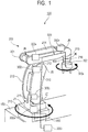
- Fig. 1 is a perspective view illustrating a robot apparatus as an example of an instrument according to an embodiment.
- a robot apparatus 100 which is the instrument, includes a robot 200 and an electronic control unit 300 0 , which is a robot control apparatus that controls the robot 200.
- the robot 200 is fixed to a mount 150.
- the robot 200 includes a vertical multi-joint robot arm 201 and a robot hand 202, which is attached to the front end of the robot arm 201 and serves as an end effector that is a terminal portion of the robot 200.
- the robot arm 201 includes a plurality of links 210 to 216 swingably or rotatably linked to each other via joints J1 to J6.
- the robot arm 201 includes six joints J1 to J6 including four joints that each swing and two joints that each rotate.
- a joint that swings is called a swing joint
- a joint that rotates is called a rotary joint.
- the joints J1 and J6 are each the rotary joint
- the joints J2, J3, J4, and J5 are each the swing joint.
- the joint J1 allows the link 211 to rotate relative to the link 210 in opposite directions by at least 360 degrees
- the joint J6 allows the link 216 to rotate relative to the link 215 in opposite directions by at least 360 degrees.
- the joints J1 to J6 of the robot arm 201 are provided with drive apparatuses that are not illustrated but drive the joints and electronic control units 300 1 to 300 6 , which control the drive apparatuses.
- the drive apparatuses that are not illustrated each include a motor and a speed reducer.
- the electronic control units 300o to 300 6 are connected to each other via a bus wire 310 in a communicable manner to form a bus communication system 320.
- the bus wire 310 is so provided as to be routed through one of the interior and exterior of the robot arm 201.
- the electronic control unit 300 0 outputs to each of the electronic control units 300 1 to 300 6 via the bus wire 310 a data signal (digital signal) carrying a position instruction value representing a target rotary position of the shaft of the motor.
- the electronic control units 300 1 to 300 6 each acquire a value detected with a rotary encoder attached to the motor and controls the rotation of the motor in such a way that the detected value approaches the input position instruction value. Further, the electronic control units 300 1 to 300 6 each output a data signal (digital signal) carrying the detected value to the electronic control unit 300o via the bus wire 310.
- a control area network (CAN) is employed to achieve high-speed communication of a large amount of data.
- the electronic control units 300 0 to 300 6 are each a node connected to the bus wire 310.
- the electronic control units 300o to 300 6 are collectively called electronic control units 300.
- Fig. 2 is a descriptive diagram illustrating the configuration of each of the electronic control units according to the embodiment.
- the electronic control units 300 each include a central processing unit (hereinafter referred to as CPU) 301, a CAN controller 302, and a CAN transceiver 303.
- the bus wire 310 includes a pair of signal lines 311 and 312.
- the CPU 301 performs a variety of types of computation necessary for the control of the robot 200 and other types of processing, issues a communication instruction to the CAN controller 302 when communication with another node is necessary, and processes data to be transmitted and data having been received.
- the data includes a bit train including logic 0 and logic 1 and transmitted and received as a parallel signal to and from the CPU 301 and the CAN controller 302 and vice versa.
- the CAN controller 302 provides the functions of the CAN protocol, such as conversion of a message into a frame, communication arbitration, error handling, ACK transmission, and CRC checking.
- the CAN controller 302 converts the parallel signal acquired from the CPU 301 into a serial signal that is a single-end signal expressed in the form of a voltage level that is one of a high level (logic 0) and a low level (logic 1) and outputs the serial signal to the CAN transceiver 303.
- the CAN controller 302 further converts a serial signal input thereto into a parallel signal and outputs the parallel signal to the CPU 301.
- the CAN transceiver 303 provides a differential physical interface between the CAN controller 302 and the bus wire 310. That is, the CAN transceiver 303 converts the single-end signal from the CAN controller 302 into differential signals or converts differential signals into a single-end signal.
- the CAN transceiver 303 applies a relatively low potential difference to the bus wire 310 (recessive), upon reception of an input of the high-level signal representing the logic-0 data from the CAN controller 302.
- the CAN transceiver 303 upon reception of an input of the low-level signal representing the logic-1 data from the CAN controller 302, applies a relatively high potential difference to the bus wire 310 (dominant).
- the CAN transceiver 303 In the case where the bus wire 310 has a relatively high potential difference, which corresponds to the dominant state, the CAN transceiver 303 outputs a low-level voltage signal to the CAN controller 302. On the other hand, in the case where the bus wire 310 has a relatively low potential difference, which corresponds to the recessive state, the CAN transceiver 303 outputs a high-level voltage signal to the CAN controller 302.
- CAN transceiver 303 also serves to adjust and assure working current and protect the wires from ESD and other incoming noise.
- the electronic control units (nodes) 300 connected to one another via the bus wire 310 need to communicate with one another, data to be transmitted is delivered from the CPU 301 to the CAN controller 302.
- the CAN controller 302 controls the CAN transceiver 303 in accordance with the CAN protocol to provide the bus wire 310 with a voltage difference (differential signals).
- the CAN transceiver 303 at each of the nodes converts the potential difference in the bus wire 310 into a single-end signal, which is processed by the CAN controller 302 in accordance with the protocol, and only data necessary for the CPU 301 is delivered thereto. Communication among the electronic control units (nodes) 300 connected to one another via the bus wire 310 is thus achieved.
- Fig. 3 is a descriptive diagram illustrating the bus communication system 320 according to the embodiment.
- the bus wire 310 is physically divided into a plurality of bus wires 310 1 , 310 2 , and 3013, as illustrated in Fig. 3 .
- a signal transmission system 450 which performs wireless communication, is disposed between the bus wire 310 1 and the bus wire 310 2 and between the bus wire 310 2 and the bus wire 310 3 .
- the signal transmission systems 450 each include a pair of signal transmission apparatuses 400 1 and 400 2 , which wirelessly communicate with each other (non-contact communication).
- the signal transmission systems 450 are disposed in the joints J1 and J6.
- the electronic control unit 300 0 and the electronic control units 300 1 , 300 2 , 300 3 , 300 4 , 300 5 , and 300 6 perform data communication via the signal transmission systems 450 disposed in the joints J1 and J6.
- a terminating resistor 315 is provided at each of the opposite ends of each of the bus wires 310 1 to 310 3 .
- the terminating resistors 315 prevent reflection of a signal at each of the opposite ends of each of the bus wires 310 1 to 310 3 , whereby the voltage across each of the bus wires is optimized.
- the signal transmission systems 450 disposed in the joints J1 and J6 have the same configuration, and the following description will therefore be made of the signal transmission system 450 disposed in the joint J1, which is one of the joints J1 and J6. Further, the following description will be made of a case where data communication is performed between the electronic control units 300o and 300 1 for ease of description.
- the signal transmission system 450 is disposed in each of the rotary joints of the robot arm 201, the signal transmission system 450 may instead be disposed in at least one of the rotary joints.
- the signal transmission system 450 may be disposed in one of the joints J1 and J6, and a toggle wire or a slip ring may be used in the other joint.
- Fig. 4 is a descriptive diagram illustrating each of the signal transmission systems according to the embodiment.
- Fig. 4 illustrates the signal transmission system 450 provided in the joint J1, which is a rotary joint, and including a pair of signal transmission apparatuses.
- the bus wire 310 1 includes a pair of signal lines 311 1 and 312 1
- the bus wire 310 2 includes a pair of signal lines 311 2 and 312 2 .
- the signal transmission system 450 includes a signal transmission apparatus 400 1 , which is connected to the bus wire 310 1 , and a signal transmission apparatus 400 2 , which is connected to the bus wire 310 2 .
- the communication counterpart of the signal transmission apparatus 400 1 is the signal transmission apparatus 400 2
- the communication counterpart of the signal transmission apparatus 400 2 is the signal transmission apparatus 400 1 .
- Short-range bidirectional communication is therefore performed between the pair of signal transmission apparatuses 400 1 and 400 2 .
- the signal transmission apparatus 400 1 includes a communication controller including a processor 401 1 , which is connected to the bus wire 310 1 , and a logic circuit 402 1 , which is a controller connected to the processor 401 1 , and a transceiver including a transmitter 403 1 and a receiver 404 1 , which are connected to the logic circuit 402 1 .
- the processor 401 1 has the same configuration as that of the CAN transceiver 303 and operates in accordance with the CAN protocol. That is, the processor 401 1 outputs a logic signal (single-end signal) having one of the low level, which is a first level representing that a signal is present, and the high level, which is a second level representing that no signal is present, in accordance with the potential difference in the bus wire 310 1 to the logic circuit 402 1 . Further, the processor 401 1 gives the bus wire 310 1 a potential difference (differential signals) according to a logic signal (single-end signal) input from the logic circuit 402 1 .
- the processor 401 1 outputs the high-level logic signal to the logic circuit 402 1 when the potential difference in the bus wire 310 1 is no greater than 0.5 [V], which corresponds to the recessive state.
- the processor 401 1 outputs the low-level logic signal to the logic circuit 402 1 when the potential difference in the bus wire 310 1 is at least 0.9 [V], which corresponds to the dominant state.
- the output impedance from the processor 401 1 to the bus wire 310 1 is set at the high impedance.
- the processor 401 1 causes current to flow through the bus wire 310 1 to set the state of the bus wire 310 1 to be the dominant state.
- the configuration of the processor 401 1 will be specifically described.
- the processor 401 1 includes a converter 410 1 , a transistor 411 1 , which is a first switching element, a transistor 412 1 , which is a second switching element, and a driver 413 1 .
- the converter 410 1 outputs the low-level (first-level) logic signal to the logic circuit 402 1 when the bus wire 310 1 has a relatively high potential difference, which corresponds to the dominant state.
- the converter 410 1 outputs the high-level (second-level) logic signal to the logic circuit 402 1 when the bus wire 310 1 has a relatively low potential difference, which corresponds to the recessive state.
- the transistors 411 1 and 412 1 are each, for example, any of a bipolar transistor, an FET (MOSFET, for example), and an IGBT.
- the transistor 411 1 is connected to the signal line 311 1 , which is one of the pair of signal lines that form the bus wire 310 1 , and a power line 310V, to which DC voltage Vcc is applied, in such a way that the transistor 411 1 is located between the signal line 311 1 and the power line 310V.
- the transistor 411 1 in the ON state causes the signal line 311 1 to be electrically continuous with the power line 310V, and the transistor 411 1 in the OFF state cuts the electrical continuity between the signal line 311 1 and the power line 310V.
- a circuit element such as a resistive element, may be connected in series to the transistor 411 1 .
- the transistor 412 1 is connected to the signal line 312 1 , which is the other one of the pair of signal lines that form the bus wire 310 1 , and a ground line 310G in such a way that the transistor 412 1 is located between the signal line 312 1 and the ground line 310G.
- the transistor 412 1 in the ON state causes the signal line 312 1 to be electrically continuous with the ground line 310G, and the transistor 412 1 in the OFF state cuts the electrical continuity between the signal line 312 1 and the ground line 310G.
- a circuit element, such as a resistive element may be connected in series to the transistor 411 2 .
- cut means that the amount of current flowing through any of the switching elements is smaller than the amount in the ON state of the switching element. For example, even in a state in which the gate (base) of the switching element is not driven, leakage current is present between the drain and the source (emitter and collector) of the switching element. The term “cut” therefore includes the state in which the leakage current flows.
- the driver 413 1 turns off the transistors 411 1 and 412 1 when the high-level (second-level) logic signal is input from the logic circuit 402 1 to the driver 413 1 .
- the transistors 411 1 and 412 1 operate in the OFF state, the current supply to the bus wire 310 1 via the transistors 411 1 and 412 1 is cut, and when no potential difference is applied from the electronic control unit 300 0 , the bus wire 310 1 operates in the recessive state.
- the driver 413 1 turns on the transistors 411 1 and 412 1 .
- the transistors 411 1 and 412 1 operate in the ON state, the current sequentially flows through the power line 310V, the transistor 411 1 , the signal line 311 1 of the bus wire 310 1 , the terminating resistor 315, the signal line 312 1 of the bus wire 310 1 , the transistor 412 1 , and the ground line 310G.
- the pair of signal lines 311 1 and 312 1 are thus given a potential difference, so that the bus wire 310 1 operates in the dominant state.
- the transmitter 403 1 includes a light emitting element 421 1 , which emits (transmits) an optical signal as a radio signal, and a light emission circuit 422 1 connected to the light emitting element 421 1 , which controls the intensity of the light emitted from the light emitting element 421 1 .
- the light emitting element 421 1 is an LED, more specifically, an infrared light emitting diode.
- the light emission circuit 422 1 receives input of a signal representing one of a transmission flag (logic 1) and a non-transmission flag (logic 0) from the logic circuit 402 1 .
- the light emission circuit 422 1 causes the light emitting element 421 1 to emit light having at least predetermined intensity when the signal representing the transmission flag (logic 1) is input from the logic circuit 402 1 to the light emission circuit 422 1 .
- the light emission circuit 422 1 causes the light emitting element 421 1 to emit no light or causes the light emitting element 421 1 to emit light having intensity lower than predetermined intensity when the signal representing the non-transmission flag (logic 0) is input from the logic circuit 402 1 .
- the transmitter 403 1 therefore transmits a radio signal (optical signal) when the signal representing the transmission flag (logic 1) is input from the logic circuit 402 1 to the transmitter 403 1 .
- a radio signal optical signal
- the transmitter 403 1 transmits no radio signal.
- the transmission of a radio signal means transmission of a signal having at least predetermined amplitude, and no transmission of a radio signal also includes transmission of a signal having amplitude smaller than the predetermined value.
- the signal representing the logic-0 flag is, for example, the low-level voltage signal
- the signal representing the logic-1 flag is, for example, the high-level voltage signal
- the receiver 404 1 includes a light receiving element 431 1 , which receives an optical signal as a radio signal, and a light reception circuit 432 1 connected to the light receiving element 431 1 .
- the light receiving element 431 1 is one of a photodiode and a phototransistor.
- the light reception circuit 432 1 produces an electric signal having amplitude (voltage level) according to the intensity of the light received with the light receiving element 431 1 .
- the light reception circuit 432 1 compares the produced electric signal with a threshold and outputs a signal carrying one of a reception flag (logic 1) representing that a radio signal has been received and a non-reception flag (logic 0) representing that no radio signal has been received to the logic circuit 402 1 .
- the light reception circuit 432 1 determines that a radio signal has been received and outputs the reception flag (logic 1) to the logic circuit 402 1 .
- the light reception circuit 432 1 determines that no radio signal has been received and outputs the non-reception flag (logic 0) to the logic circuit 402 1 .
- the logic 0 carried by the flag transmitted and received in the communication between the logic circuit 402 1 and the transmitter 403i/receiver 404 1 represents a relatively weak light state, whereas the logic 1 represents a relatively strong light state.
- the receiver 404 1 when the receiver 404 1 has received a radio signal (in the strong light state), the receiver 404 1 outputs the reception flag (logic 1) representing that a radio signal has been received to the logic circuit 402 1 . On the other hand, when the receiver 404 1 has received no radio signal (in the weak light state), the receiver 404 1 outputs the non-reception flag (logic 0) representing that no radio signal has been received to the logic circuit 402 1 .
- the signal representing the logic-0 flag is, for example, the low-level voltage signal
- the signal representing the logic-1 flag is, for example, the high-level voltage signal
- the logic circuit 402 1 has two input ports IN1 and IN2 and two output ports OUT1 and OUT2.
- the first input port IN1 is connected to the converter 410 1 in the processor 401 1
- the second input port IN2 is connected to the light reception circuit 432 1 in the receiver 404 1 .
- the first output port OUT1 is connected to the driver 413 1 in the processor 401 1
- the second output port OUT2 is connected to the light emission circuit 422 1 in the transmitter 403 1 .
- the logic circuit 402 1 receives input of one of the high-level logic signal and the low-level logic signal from the converter 410 1 in the processor 401 1 via the input port IN1.
- the logic circuit 402 1 receives input of one of the logic-0 logical frag (signal) and the logic-1 logical flag from the light reception circuit 432 1 in the receiver 404 1 via the input port IN2.
- the logic circuit 402 1 produces one of the high-level logic signal and the low-level logic signal and outputs the logic signal to the driver 413 1 in the processor 401 1 via the output port OUT1.
- the logic circuit 402 1 produces the logical flag having one of the logic 0 representing the non-transmission flag and the logic 1 representing the transmission flag and outputs a signal representing the logical flag to the light emission circuit 422 1 in the transmitter 403 1 via the output port OUT2.
- the signal transmission apparatus 400 2 has the same configuration as that of the signal transmission apparatus 400 1 . That is the signal transmission apparatus 400 2 includes a communication controller including a processor 401 2 , which is connected to the bus wire 310 2 , and a logic circuit 402 2 , which is a controller connected to the processor 401 2 , and a transceiver including a transmitter 403 2 and a receiver 404 2 , which are connected to the logic circuit 402 2 .
- the processor 401 2 includes a converter 410 2 , a transistor 411 2 , which is the first switching element, a transistor 412 2 , which is the second switching element, and a driver 413 2 .
- the transmitter 403 2 includes a light emitting element 421 2 and a light emission circuit 422 2
- the receiver 404 2 includes a light receiving element 431 2 and a light reception circuit 432 2 .
- the transmitters 403 1 and 403 2 and the receivers 404 1 and 404 2 form another wireless communication unit 440.
- Fig. 5A is a perspective view illustrating the driving apparatus disposed in the joint J1, which is a rotary joint, of the robot arm.
- the joint J6, which is another rotary joint, has the same configuration and will not therefore be described.
- a driving apparatus 250 drives and rotates the link 211, which is one of the pair of the links 210 and 211, relative to the other link 210 and includes a motor (and speed reducer).
- a cylindrical member 501 which is a first member, is securely attached to the stator of the driving apparatus 250.
- the shaft member 502 is so disposed in the cylindrical member 501 as to be coaxial with the cylindrical member 501 and rotates relative to the cylindrical member 501 around a center axis C1 of the cylindrical member 501.
- One of the cylindrical member 501 and the shaft member 502 is fixed to the link 210, and the other is fixed to the link 211.
- Fig. 5B is a descriptive diagram illustrating the arrangement of one set of the light emitting elements and light receiving elements.
- the light emitting element 421 1 and the light receiving element 431 1 of the signal transmission apparatus 400 1 are disposed as part of one of the cylindrical member 501 and the shaft member 502, specifically, in the cylindrical member 501 in the present embodiment. More specifically, the light emitting element 421 1 and the light receiving element 431 1 are fixed to the inner circumferential surface of the cylindrical member 501.
- the light emitting element 421 2 and the light receiving element 4312 of the signal transmission apparatus 400 2 are disposed as part of the other one of the cylindrical member 501 and the shaft member 502, specifically, on the shaft member 502 in the present embodiment. More specifically, the light emitting element 421 2 and the light receiving element 431 2 are fixed to the outer circumferential surface of the shaft member 502.
- the transmission counterpart of the light emitting element 421 1 disposed in the cylindrical member 501 is the light receiving element 431 2 disposed on the shaft member 502.
- the transmission counterpart of the light emitting element 421 2 disposed on the shaft member 502 is the light receiving element 431 1 disposed in the cylindrical member 501.
- the configuration described above allows non-contact communication.
- the light emitting element 421 1 , the light emitting element 421 2 , the light receiving element 431 1 , and the light receiving element 431 2 are disposed in the same space that serves as the wireless transmission path, whereby space saving is achieved.
- the size and weight of the robot arm 201 can thus be reduced, whereby the controllability of the robot arm 201 is improved.
- the space in which the pair of the light emitting element 421 1 and the light receiving element 431 2 are disposed and the space in which the pair of the light emitting element 421 2 and the light receiving element 431 1 are disposed may not be separate from each other.
- the wavelength of the light used in the communication between the light emitting element 421 1 and the light receiving element 431 2 may not differ from the wavelength of the light used in the communication between the light emitting element 421 2 and the light receiving element 431 1 . Therefore, the light emitting elements 421 1 and 421 2 can be formed of elements (LEDs, for example) compliant with the same standard, and the light receiving elements 431 1 and 431 2 can be formed of elements (PDs, for example) compliant with the same standard.
- the logic circuits 402 1 and 402 2 of the signal transmission apparatuses 400 1 and 400 2 operate as shown in the following conditions in the wireless transmission operation.
- Condition 1 When the logical high level is input to the input port IN1, the logic 0 is output via the output port OUT2.
- Condition 2 When the logic 0 is input to the input port IN2, the logical high level is output via the output port OUT1.
- Condition 3 When the logic 0 is input to the input port IN2 and the logical level input to the input port IN1 transitions from the logical high level to the logical low level, the logical level output via the output port OUT1 is held at the logical high level and the logic output via the output port OUT2 is held at the logic 1. The logic holding operation is performed until the logical level input to the input port IN1 transitions from the logical low level to the logical high level irrespective of the logical state of the input to the input port IN2.
- Condition 4 When the logical high level is input to the input port IN1 and the logic input to the input port IN2 transitions from the logic 0 to the logic 1, the logical level output via the output port OUT1 is held at the logical low level and the logic output via the output port OUT2 is held at the logic 0. The logic holding operation is performed until the logic input to the input port IN2 transitions from the logic 1 to the logic 0 irrespective of the logical state of the input to the input port IN1.
- Condition 5 After the conditions 3 and 4 are satisfied, the logic output via the output port OUT2 is set at the logic 1 when the logical level input to the input port IN1 is the logical low level, and the logical level output via the output port OUT1 is set at the logical low level when the logic input to the input port IN2 is the logic 1.
- the wireless communication unit 440 including the transmitters 403 1 and 403 2 and the receivers 404 1 and 404 2 illustrated in Fig. 4 has a logical sum configuration.
- the logic 1 is output to the input port IN2 of both the logic circuits 402 1 and 402 2 connected to the wireless communication unit 440. That is, only when the input from the logic circuits 402 1 and 402 2 connected to the wireless communication unit 440 is the logic 0, the logic 0 is input to the input port IN2 of both the logic circuits 402 1 and 402 2 connected to the wireless communication unit 440.
- Figs. 6A to 6D are descriptive diagrams illustrating the actions of the signal transmission apparatuses 400 1 and 400 2 in the transmission of a signal from the bus wire 310 1 , which part of the bus wire 310, to the bus wire 310 2 , which is another part of the bus wire 310.
- Figs. 7A to 7D are descriptive diagrams illustrating the actions of the signal transmission apparatuses 400 1 and 400 2 at the end of the transmission of the signal from the bus wire 310 1 , which part of the bus wire 310, to the bus wire 310 2 , which is another part of the bus wire 310.
- Fig. 8A illustrates a truth table of the input to and the output from each of the logic circuits. Fig.
- Fig. 9A is a time chart illustrating the action of the logic circuit in one of the signal transmission apparatuses.
- Fig. 9B is a time chart illustrating the action of the logic circuit in the other signal transmission apparatus.
- the bus wires 310 1 and 310 2 both operate in the recessive state. That is, since the electronic control unit 300 0 outputs no differential signals (potential difference), the converters 410 1 and 410 2 output the logic signal having the high level H to the logic circuits 402 1 and 402 2 .
- the logic circuits 402 1 and 402 2 therefore each receive input of the logic signal having the high level H via the input port IN1 and input of the logic-0 flag via the input port IN2.
- the logic circuit 402 1 sets the logical level output via the output port OUT1 to be the high level H and the logic output via the output port OUT2 to be the logic 0 (state S0), as illustrated in Fig. 8A .
- the logic circuit 402 1 outputs the logic signal having the high level H via the output port OUT1 to the driver 413 1 and outputs the logic-0 flag via the output port OUT2 to the transmitter 403 1 , as illustrated in Fig. 8A .
- the driver 413 1 receives the input of the logic signal having the high level H and turns off the transistors 411 1 and 412 1 .
- the transmitter 403 1 receives the input of the logic-0 flag and transmits no radio signal. The same holds true for the logic circuit 402 2 .
- the logic circuits 402 1 and 402 2 operate in the S0 state, as illustrated in Figs. 8B , 9A, and 9B .
- the transition of the states of the logic circuits 402 1 and 402 2 differ from each other depending on whether the logic circuits transmit or receive a data signal. Specifically, the upper route in Fig. 8B illustrates the transition of the state of the logic circuit 402 1 , and the lower route in Fig. 8B illustrates the transition of the state of the logic circuit 402 2 .
- the converter 410 1 outputs the logic signal having the low level L to the logic circuit 402 1 , as illustrated in Fig. 6B .
- the input of the logic signal to the input port IN1 transitions from the high level H to the low level L at the timing T1.
- the logic signal having the low level L is therefore input from the converter 410 1 to the logic circuit 402 1 via the input port IN1 with the logic-0 flag input to the logic circuit 402 1 via the input port IN2.
- the logic circuit 402 1 sets the logical level output via the output port OUT1 to be the high level H and the logic output via the output port OUT2 to be the logic 1 (state S1), as illustrated in Fig. 8A . That is, in a case where the logic signal having the low level L is input to the logic circuit 402 1 from the converter 410 1 with no logic-1 flag (but logic-0 flag) input to the logic circuit 402 1 from the receiver 404 1 , the logic circuit 402 1 outputs the logic 1, which is the transmission flag, to the transmitter 403 1 . More specifically, in the input state illustrated in Fig.
- the logic circuit 402 1 outputs the logic signal having the high level H to the driver 413 1 via the output port OUT1 and outputs the logic-1 flag representing the transmission flag to the transmitter 403 1 via the output port OUT2. As described above, the logic circuit 402 1 causes the light emitting element 421 1 of the transmitter 403 1 to transmit the optical signal but the transistors 411 1 and 412 1 to keep operating in the OFF state.
- the light receiving elements 431 1 and 431 2 in the receivers 404 1 and 404 2 receive the optical signals, as illustrated in Fig. 6C .
- the light reception circuits 432 1 and 432 2 in the receivers 404 1 and 404 2 therefore output the logic-1 flag representing the reception flag to the logic circuits 402 1 and 402 2 .
- the logic-1 flag representing the reception flag is input to the logic circuits 402 1 and 402 2 at the timing T2, which is behind the timing T1, when the logic circuits 402 1 and 402 2 receive the logic signal having the low level L, as illustrated in Figs. 9A and 9B .
- the logic circuit 402 1 sets the logical level output via the output port OUT1 to be the high level H and the logic output via the output port OUT2 to be the logic 1 (state S2), as illustrated in the truth table illustrated in Fig. 8A . That is, in the input state illustrated in Fig. 6C , the logic circuit 402 1 outputs the logic signal having the high level H to the driver 413 1 via the output port OUT1 and outputs the logic-1 flag representing the transmission flag to the transmitter 403 1 via the output port OUT2.
- the logic circuit 402 1 has received the radio signal from the transmitter 403 1 of the signal transmission apparatus to which the logic circuit 402 1 belongs.
- the logic circuit 402 1 therefore controls the transistors 411 1 and 412 1 to be maintained in the OFF state with the transmission action maintained.
- the bus wire 310 1 is therefore not current-driven by the electronic control unit 300 0 and the signal transmission apparatus 400 1 at the same time.
- the bus wire 310 1 operates in the dominant state because the electronic control unit 300 0 supplies differential signals.
- the bus wire 310 1 transitions from the dominant state to the recessive state because the transistors 411 1 and 412 1 are maintained in the OFF state. A situation in which the signal transmission apparatus 400 1 itself accidentally sets the state of the bus wire 310 1 to be the dominant state can thus be avoided.
- the logic circuit 402 2 sets the logical level output via the output port OUT1 to be the low level L and the logic output via the output port OUT2 to be the logic 0 (state S4), as illustrated in the truth table illustrated in Fig. 8A . That is, at the timing T2 illustrated in Fig. 9B , the logic signal input from the converter 410 2 to the logic circuit 402 2 has the state having the high level H.
- the logic circuit 402 2 switches the logical level of the logic signal to be output to the driver 413 2 from the high level H to the low level L (state S4). That is, in the input state illustrated in Fig. 6C , the logic circuit 402 2 outputs the logic signal having the low level L to the driver 413 2 via the output port OUT1 and outputs the logic-0 flag representing the non-transmission flag to the transmitter 403 2 via the output port OUT2.
- the driver 413 2 to which the logic signal having the low level L has been input turns on the transistors 411 1 and 412 1 , as illustrated in Fig. 6D .
- the bus wire 310 2 therefore transitions from the recessive state to the dominant state.
- the electronic control unit 300 0 then inputs differential signals to the electronic control unit 300 1 . Since the bus wire 310 2 has transitioned from the recessive state to the dominant state, the converter 410 2 sets the logical level of the logic signal to be output to the logic circuit 402 2 to be the low level L.
- the logic circuit 402 2 sets the logical level output via the output port OUT1 to be the low level L and the logic output via the output port OUT2 to be the logic 0 (state S5), as illustrated in the truth table illustrated in Fig. 8A . That is, in the input state illustrated in Fig. 6D , the logic circuit 402 2 outputs the logic signal having the low level L to the driver 413 2 via the output port OUT1 and outputs the logic-0 flag representing the non-transmission flag to the transmitter 403 2 via the output port OUT2.
- the logic circuit 402 2 therefore holds the logical level of the logic signal to be output to the driver 413 2 at the low level L and holds the flag to be transmitted to the transmitter 403 2 to be the logic-0 flag until the state of the logic circuit 402 2 transitions to the state in which the logic circuit 402 2 receives the logic-0 flag from the receiver 404 2 .
- the logic circuit 402 2 causes the transmitter 403 2 to transmit no radio signal even when the logic signal having the low level L is input to the logic circuit 402 2 from the converter 410 2 because the electronic control unit 300 1 has not set the state of the bus wire 310 2 to be the dominant state. Therefore, even when the bus wire 310 2 transitions from the recessive state to the dominant state, malfunction of transmission of a radio signal from the transmitter 403 2 can be avoided.
- the logic circuit 402 1 evaluates whether the radio signal received with the receiver 404 1 is a radio signal transmitted from the communication counterpart or a radio signal transmitted from the transmitter 403 1 . In the case where the radio signal received with the receiver 404 1 is a radio signal transmitted from the communication counterpart, the logic circuit 402 1 operates in such a way the logic signal having the low level L is output to the driver 413 1 . On the other hand, in the case where the radio signal received with the receiver 404 1 is a radio signal transmitted from the transmitter 403 1 , the logic circuit 402 1 operates in such a way that the logic signal having the high level H is output to the driver 413 1 .
- the logic circuit 402 1 performs the evaluation described above based on whether the logic signal input from the converter 410 1 has the high level L or the low level L when the logic 1 is input from the receiver 404 1 to the logic circuit 402 1 .
- the radio signal is a radio signal transmitted from the transmitter 403 1 of the signal transmission apparatus to which the logic circuit 402 1 belongs, whereas when the logic signal has the high level H, the radio signal is a radio signal transmitted from the transmitter 403 2 of the communication counterpart. Therefore, in the CAN bus communication, malfunction of the signal transmission apparatus 400 1 can be avoided even when a radio signal transmitted from the transmitter 403 1 of one of signal transmission apparatuses is received with the receiver 404 1 of the same signal transmission apparatus. The same holds true for the signal transmission apparatus 400 2 including the logic circuit 402 2 .
- the converter 410 1 changes the logic signal to be output to the logic circuit 402 1 from the low level L to the high level H.
- the logic signal input to the input port IN1 transitions from the low level L to the high level H at the timing T3.
- the logic signal having the high level H is therefore input from the converter 410 1 to the logic circuit 402 1 with the logic-1 flag input from the receiver 404 1 to the logic circuit 402 1 .
- the logic circuit 402 1 sets the logical level output via the output port OUT1 to be the high level H and the logic output via the output port OUT2 to be the logic 0 (state S3), as illustrated in Fig. 8A .
- the transmitter 403 1 lowers the intensity of the emitted light after the logic-0 flag is output from the logic circuit 402 1 .
- the receiver 404 1 then outputs the logic-0 flag to the logic circuit 402 1 after the intensity of the received emitted light lowers. It is therefore determined that the bus wire 310 1 receives the radio signal in the recessive state from the point of time when the logic signal having the high level H is input from the converter 410 1 to the logic circuit 402 1 to the point of time when the logic-0 flag is input from the receiver 404 1 to the logic circuit 402 1 .
- the logic circuit 402 1 should therefore avoid false recognition that the received radio signal has been transmitted from the communication counterpart.
- the timing T3 in Fig. 9A is the point of time when the logic signal input from the converter 410 1 to the logic circuit 402 1 transitions from the low level L to the high level H with the logic-1 flag input from the receiver 404 1 to the logic circuit 402 1 . Further, the timing T4 in Fig. 9A is the point of time when the logical flag input from the receiver 404 1 to the logic circuit 402 1 switches from the logic 1 to the logic 0.
- the logic circuit 402 1 holds the logic signal to be output to the driver 413 1 at the high level H for the period from the timing T3 to the timing T4, as illustrated in Fig. 7C . Since the logic signal to the driver 413 1 is held at the high level H, the transistors 411 1 and 412 1 are held in the OFF state, and the bus wire 310 1 is held in the recessive state. Therefore, in the signal transmission apparatus 400 1 , accidental change of the state of the bus wire 310 1 to the dominant state for the period from the timing T3 to the timing T4 can be avoided.
- the logic circuit 402 2 outputs the logic signal having the high level H via the output port OUT1, as illustrated in Fig. 7C , when the flag input from the receiver via the input port IN2 transitions from the logic 1 to the logic 0 at the timing T4 illustrated in Fig. 9B .
- the logic circuit 402 2 outputs the logic signal having the high level H in order to switch the state of the bus wire 310 2 from the dominant state to the recessive state because there is no radio signal from the communication counterpart.
- the logic circuit 402 1 sets the logical level output via the output port OUT1 to be the high level H and the logic output via the output port OUT2 to be the logic 0 (state S6), as illustrated in Fig. 8A .
- the driver 413 2 switches the states of the transistors 411 2 and 412 2 to the OFF state in response to the input of the logic signal having the high level H.
- the state of the bus wire 310 2 therefore changes to the recessive state.
- the converter 410 2 switches the logical level of the logic signal to be output to the logic circuit 402 2 from the low level L to the high level H.
- the timing T4 in Fig. 9B is the point of time when the flag input from the receiver 404 2 to the logic circuit 402 2 transitions from the logic 1 to the logic 0 with the logic signal input from the converter 410 2 to the logic circuit 402 2 .
- the timing T5 in Fig. 9B is the point of time when the logic signal input from the converter 410 2 to the logic circuit 402 2 transitions from the low level L to the high level H.
- the logic circuit 402 2 therefore outputs no transmission flag to the transmitter 403 2 , that is, outputs the logic-0 flag for the period from the timing T4 to the timing T5, that is, until the logic signal having the high level H is input to the logic circuit 402 2 , as illustrated in Fig. 7D . Therefore, for the period from the timing T4 to timing T5, the logic circuit 402 2 can avoid false recognition that data has been transmitted from the electronic control unit 300 1 , whereby malfunction of the signal transmission apparatus 400 2 can be avoided.
- the logic circuit 402 2 sets the logical level output via the output port OUT1 to be the high level H and the logic output via the output port OUT2 to be the logic 0 (state S0).
- the logic circuit 402 1 and 402 2 each include a plurality of logic elements.
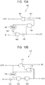
- Figs. 10A and 10B are circuit diagrams illustrating the configurations of the logic circuits.
- the logic circuit 402 1 and 402 2 each have one of the circuit configurations illustrated in Figs. 10A and 10B .
- the logic circuit 402 1 and 402 2 are each drawn in the form of a logic circuit 402.
- the logic circuit 402 includes a plurality of logic elements 461 to 466 and a delay circuit 467.
- the logic element 461 is a NOT element.
- the logic element 462 is an OR element.
- the logic element 463 is a NOT element.
- the logic element 464 is an OR element.
- the logic element 465 is a NOT element.
- the logic element 466 is an AND element.
- the logic circuit 402 includes a plurality of logic elements 471 to 475 and a delay circuit 476.
- the logic elements 471 and 473 to 475 are each an AND element.
- the logic element 472 is a NOT element.
- the logic circuits 402 1 and 402 2 can each be achieved by basic logic gates and can therefore be each readily formed at low cost.
- one of the delay circuit 467 illustrated in Fig. 10A and the delay circuit 476 has the function of correcting the delay.
- the delay circuits 467 and 476 can each be readily achieved, for example, by a lowpass filter including a resistor and a capacitor and each do not necessarily have a specific configuration as long as the amount of delay roughly equal to the delay described above is provided.
- the logic circuit 402 1 and 402 2 each do not necessarily have the configuration illustrated in one of Figs. 10A and 10B and only need to have the function described above, and the logic circuit 402 1 and 402 2 may not have the same configuration.
- the present invention is not limited to the embodiment described above, and many variations are conceivable within the technical sprit of the present invention. Further, the effects described in the embodiment are only a list of most preferable effects provided by the present invention, and the effects provided by the present invention are not limited to those described in the embodiment.
- optical communication can be performed, but the communication may be performed based on one of a radio wave, an electric field, and a magnetic field.
- the transmitter may be formed of a resonator and a modulator
- the receiver may be formed of a resonator and a demodulator.
- the present invention can also be implemented in the form of the process of supplying one of a system and an apparatus with a program that achieves at least one of the functions of the embodiment described above via one of a network and a storage medium and causing at least one processor in a computer of one of the system and the apparatus to read and execute the program.
- the present invention can still instead be achieved in the form of a circuit (ASIC, for example) that achieves at least one of the functions.
Landscapes
- Engineering & Computer Science (AREA)
- Computer Networks & Wireless Communication (AREA)
- Signal Processing (AREA)
- Physics & Mathematics (AREA)
- Electromagnetism (AREA)
- Power Engineering (AREA)
- Robotics (AREA)
- Mechanical Engineering (AREA)
- Manipulator (AREA)
- Optical Communication System (AREA)
- Bidirectional Digital Transmission (AREA)
- Dc Digital Transmission (AREA)
Abstract
Description
- The present invention relates to a signal transmission apparatus, a signal transmission system, and an instrument that wirelessly transmit a signal in bus communication.
- To enhance the function and performance of an automobile, a large number of electronic control units (ECUs) have been employed. If these ECUs are connected to each other and allowed to communicate with each other, a tremendous amount of wiring is required, resulting in increase in weight and cost. To reduce the amount of wiring and satisfy a requirement of high-speed communication of a large amount of data, a control area network (CAN) has been developed.
- In recent years, it has been recognized that a CAN has high reliability, for example, in a failure detection function, and a CAN is therefore used in a variety of fields, such as elevators, railways, airplanes, ships, and medical instruments. Further, there is also a case where a CAN is used in a manufacturing apparatus and an inspection apparatus installed, for example, in a factory to achieve distributed control in the apparatuses.
- On the other hand, in a production line, for example, in a factory, an industrial robot performs assembly and other types of work. The robot includes a multi-joint robot arm and an end effector provided as the front end of the robot arm. A drive control apparatus that controls a driving apparatus that drives each of the joints of the robot arm is provided at the joint, and it is planned to employ a CAN for communication between each of the drive control apparatuses and the robot control apparatus.
- To incorporate bus wires in the robot arm and prevent the bus wire disconnection in a joint of the robot arm, particularly in a rotary joint, it has been necessary to use expensive dedicated wires and route the wires in a special manner.
- A rotary joint with bus wires routed therein cannot rotate endlessly, and routing the bus wires therefore restricts the action of the robot arm, resulting in a decrease in the flexibility of the action of the robot arm.
- To avoid the problem, it is conceivable to use a slip ring to achieve endless rotation, but the slip ring uses a mechanical contact, resulting in a problem of increase in weight and size of the robot. Further, the slip ring needs to undergo frequent maintenance to avoid contact failure due to wear of the brush and other components.
- To achieve a non-contact CAN bus,
Patent Literature 1 proposes a configuration in which a signal transmission apparatus wirelessly transmits a signal. InPatent Literature 1, a pair of remote coupler apparatuses are provided as the signal transmission apparatus, and the pair of remote coupler apparatuses wirelessly connect a pair of bus wires to each other. The remote coupler apparatuses each include an input/output signal control apparatus, a modulator, a resonator, and a demodulator. - PTL 1: International Publication No.
WO09/133633 - The remote coupler apparatuses described in
Patent Literature 1 are so adapted that a radio signal transmitted from the resonator connected to the modulator in one of the remote coupler apparatuses is received with the resonator connected to the demodulator of the other remote coupler apparatus. However, due to the restriction resulting from the arrangement of the modulators, demodulators, and resonators, there is a situation in which the resonator connected to the modulator of the one remote coupler apparatus and the resonator connected to the demodulator of the same remote coupler apparatus cannot be isolated from each other. In a robot arm, for example, the remote coupler apparatuses need to be disposed in a narrow space in a joint, and there is therefore a situation in which it is difficult to isolate the resonators of the same remote coupler apparatus from each other. Under such a situation, the radio signal transmitted from the resonator connected to the modulator of one of the remote coupler apparatuses is also received with the resonator connected to the demodulator of the same remote coupler apparatus, possibly resulting in malfunction. The problem described above is not limited to the radio-wave-based wireless communication described inPatent Literature 1 and can occur in every wireless communication between a transmitter and receiver, such as wireless communication using light (infrared light, for example) and wireless communication using one of an electric field and a magnetic field. - An object of the present invention is to achieve a configuration that can avoid malfunction in bus communication even when a radio signal transmitted from a transmitter of an apparatus is received with a receiver of the same apparatus.
- According to a viewpoint of the prevent invention, a signal transmission apparatus includes a processor connected to a bus wire including a pair of signal lines, a controller connected to the processor, and a transmitter and a receiver connected to the controller. The processor produces a logic signal having one of a first level representing that a signal is present and a second level representing that no signal is present in accordance with a potential difference between the pair of signal lines. The light receiver produces a signal representing one of a reception flag and a non-reception flag in accordance with magnitude of a received radio signal. The controller controls a state of transmission of a radios signal from the transmitter based on the logic signal produced by the processor and the signal produced by the light receiver.
- The present invention can prevent malfunction in bus communication even when a radio signal transmitted from a transmitter of an apparatus is received with a receiver of the same apparatus.
- Further features of the present invention will be apparent by the description of examples described below with reference to the drawings.
-
-
Fig. 1 is a perspective view illustrating a robot apparatus as an example of an instrument according to an embodiment. -
Fig. 2 is a descriptive diagram illustrating the configuration of an electronic control unit according to the embodiment. -
Fig. 3 is a descriptive diagram illustrating a bus communication system according to the embodiment. -
Fig. 4 is a descriptive diagram illustrating a signal transmission system according to the embodiment. -
Fig. 5A is a perspective view illustrating a driving apparatus disposed in a rotary joint of a robot arm. -
Fig. 5B is a descriptive diagram illustrating the arrangement of a light emitting element and a light receiving element. -
Fig. 6A is a descriptive diagram illustrating the action of signal transmission apparatuses in the transmission of a signal from one bus wire to another bus wire. -
Fig. 6B is a descriptive diagram illustrating the action of the signal transmission apparatuses in the transmission of the signal from the one bus wire to the other bus wire. -
Fig. 6C is a descriptive diagram illustrating the action of the signal transmission apparatuses in the transmission of the signal from the one bus wire to the other bus wire. -
Fig. 6D is a descriptive diagram illustrating the action of the signal transmission apparatuses in the transmission of the signal from the one bus wire to the other bus wire. -
Fig. 7A is a descriptive diagram illustrating the action of the signal transmission apparatuses at the end of the transmission of the signal from the one bus wire to the other bus wire. -
Fig. 7B is a descriptive diagram illustrating the action of the signal transmission apparatuses at the end of the transmission of the signal from the one bus wire to the other bus wire. -
Fig. 7C is a descriptive diagram illustrating the action of the signal transmission apparatuses at the end of the transmission of the signal from the one bus wire to the other bus wire. -
Fig. 7D is a descriptive diagram illustrating the action of the signal transmission apparatuses at the end of the transmission of the signal from the one bus wire to the other bus wire. -
Fig. 8A illustrates a truth table of the input to and the output from each logic circuit. -
Fig. 8B is a descriptive diagram illustrating the transition of the states of the logic circuits. -
Fig. 9A is a time chart illustrating the action of the logic circuit in one of the signal transmission apparatuses. -
Fig. 9B is a time chart illustrating the action of the logic circuit in the other signal transmission apparatus. -
Fig. 10A is a circuit diagram illustrating the configuration of each of the logic circuits. -
Fig. 10B is another circuit diagram illustrating the configuration of each of the logic circuits. - A form for implementing the present invention will be described below in detail with reference to the drawings.
Fig. 1 is a perspective view illustrating a robot apparatus as an example of an instrument according to an embodiment. - A
robot apparatus 100, which is the instrument, includes arobot 200 and anelectronic control unit 3000, which is a robot control apparatus that controls therobot 200. Therobot 200 is fixed to amount 150. Therobot 200 includes a verticalmulti-joint robot arm 201 and arobot hand 202, which is attached to the front end of therobot arm 201 and serves as an end effector that is a terminal portion of therobot 200. - The
robot arm 201 includes a plurality oflinks 210 to 216 swingably or rotatably linked to each other via joints J1 to J6. In the present embodiment, therobot arm 201 includes six joints J1 to J6 including four joints that each swing and two joints that each rotate. A joint that swings is called a swing joint, and a joint that rotates is called a rotary joint. In therobot arm 201, the joints J1 and J6 are each the rotary joint, and the joints J2, J3, J4, and J5 are each the swing joint. The joint J1 allows thelink 211 to rotate relative to thelink 210 in opposite directions by at least 360 degrees, and the joint J6 allows thelink 216 to rotate relative to thelink 215 in opposite directions by at least 360 degrees. - The joints J1 to J6 of the
robot arm 201 are provided with drive apparatuses that are not illustrated but drive the joints andelectronic control units 3001 to 3006, which control the drive apparatuses. The drive apparatuses that are not illustrated each include a motor and a speed reducer. The electronic control units 300o to 3006 are connected to each other via abus wire 310 in a communicable manner to form abus communication system 320. Thebus wire 310 is so provided as to be routed through one of the interior and exterior of therobot arm 201. - The
electronic control unit 3000 outputs to each of theelectronic control units 3001 to 3006 via the bus wire 310 a data signal (digital signal) carrying a position instruction value representing a target rotary position of the shaft of the motor. Theelectronic control units 3001 to 3006 each acquire a value detected with a rotary encoder attached to the motor and controls the rotation of the motor in such a way that the detected value approaches the input position instruction value. Further, theelectronic control units 3001 to 3006 each output a data signal (digital signal) carrying the detected value to the electronic control unit 300o via thebus wire 310. - In the
bus communication system 320, a control area network (CAN) is employed to achieve high-speed communication of a large amount of data. In the present embodiment, theelectronic control units 3000 to 3006 are each a node connected to thebus wire 310. In the following description, the electronic control units 300o to 3006 are collectively calledelectronic control units 300. -
Fig. 2 is a descriptive diagram illustrating the configuration of each of the electronic control units according to the embodiment. Theelectronic control units 300 each include a central processing unit (hereinafter referred to as CPU) 301, aCAN controller 302, and aCAN transceiver 303. Thebus wire 310 includes a pair ofsignal lines - The
CPU 301 performs a variety of types of computation necessary for the control of therobot 200 and other types of processing, issues a communication instruction to theCAN controller 302 when communication with another node is necessary, and processes data to be transmitted and data having been received. The data includes a bittrain including logic 0 andlogic 1 and transmitted and received as a parallel signal to and from theCPU 301 and theCAN controller 302 and vice versa. - The
CAN controller 302 provides the functions of the CAN protocol, such as conversion of a message into a frame, communication arbitration, error handling, ACK transmission, and CRC checking. TheCAN controller 302 converts the parallel signal acquired from theCPU 301 into a serial signal that is a single-end signal expressed in the form of a voltage level that is one of a high level (logic 0) and a low level (logic 1) and outputs the serial signal to theCAN transceiver 303. TheCAN controller 302 further converts a serial signal input thereto into a parallel signal and outputs the parallel signal to theCPU 301. - The
CAN transceiver 303 provides a differential physical interface between theCAN controller 302 and thebus wire 310. That is, theCAN transceiver 303 converts the single-end signal from theCAN controller 302 into differential signals or converts differential signals into a single-end signal. - In a specific description, the
CAN transceiver 303 applies a relatively low potential difference to the bus wire 310 (recessive), upon reception of an input of the high-level signal representing the logic-0 data from theCAN controller 302. On the other hand, theCAN transceiver 303, upon reception of an input of the low-level signal representing the logic-1 data from theCAN controller 302, applies a relatively high potential difference to the bus wire 310 (dominant). - In the case where the
bus wire 310 has a relatively high potential difference, which corresponds to the dominant state, theCAN transceiver 303 outputs a low-level voltage signal to theCAN controller 302. On the other hand, in the case where thebus wire 310 has a relatively low potential difference, which corresponds to the recessive state, theCAN transceiver 303 outputs a high-level voltage signal to theCAN controller 302. - Further, the
CAN transceiver 303 also serves to adjust and assure working current and protect the wires from ESD and other incoming noise. - In a case where the electronic control units (nodes) 300 connected to one another via the
bus wire 310 need to communicate with one another, data to be transmitted is delivered from theCPU 301 to theCAN controller 302. TheCAN controller 302 controls theCAN transceiver 303 in accordance with the CAN protocol to provide thebus wire 310 with a voltage difference (differential signals). TheCAN transceiver 303 at each of the nodes converts the potential difference in thebus wire 310 into a single-end signal, which is processed by theCAN controller 302 in accordance with the protocol, and only data necessary for theCPU 301 is delivered thereto. Communication among the electronic control units (nodes) 300 connected to one another via thebus wire 310 is thus achieved. -
Fig. 3 is a descriptive diagram illustrating thebus communication system 320 according to the embodiment. To allow the links to freely rotate at the joints J1 and J6, thebus wire 310 is physically divided into a plurality ofbus wires Fig. 3 . Asignal transmission system 450, which performs wireless communication, is disposed between thebus wire 3101 and thebus wire 3102 and between thebus wire 3102 and thebus wire 3103. Thesignal transmission systems 450 each include a pair of signal transmission apparatuses 4001 and 4002, which wirelessly communicate with each other (non-contact communication). Thesignal transmission systems 450 are disposed in the joints J1 and J6. - That is, the
electronic control unit 3000 and theelectronic control units signal transmission systems 450 disposed in the joints J1 and J6. A terminatingresistor 315 is provided at each of the opposite ends of each of thebus wires 3101 to 3103. The terminatingresistors 315 prevent reflection of a signal at each of the opposite ends of each of thebus wires 3101 to 3103, whereby the voltage across each of the bus wires is optimized. - The
signal transmission systems 450 disposed in the joints J1 and J6 have the same configuration, and the following description will therefore be made of thesignal transmission system 450 disposed in the joint J1, which is one of the joints J1 and J6. Further, the following description will be made of a case where data communication is performed between theelectronic control units 300o and 3001 for ease of description. Although thesignal transmission system 450 is disposed in each of the rotary joints of therobot arm 201, thesignal transmission system 450 may instead be disposed in at least one of the rotary joints. For example, thesignal transmission system 450 may be disposed in one of the joints J1 and J6, and a toggle wire or a slip ring may be used in the other joint. -
Fig. 4 is a descriptive diagram illustrating each of the signal transmission systems according to the embodiment.Fig. 4 illustrates thesignal transmission system 450 provided in the joint J1, which is a rotary joint, and including a pair of signal transmission apparatuses. Thebus wire 3101 includes a pair ofsignal lines bus wire 3102 includes a pair ofsignal lines - The
signal transmission system 450 includes a signal transmission apparatus 4001, which is connected to thebus wire 3101, and a signal transmission apparatus 4002, which is connected to thebus wire 3102. The communication counterpart of the signal transmission apparatus 4001 is the signal transmission apparatus 4002, and the communication counterpart of the signal transmission apparatus 4002 is the signal transmission apparatus 4001. Short-range bidirectional communication is therefore performed between the pair of signal transmission apparatuses 4001 and 4002. - The signal transmission apparatus 4001 includes a communication controller including a processor 4011, which is connected to the
bus wire 3101, and alogic circuit 4021, which is a controller connected to the processor 4011, and a transceiver including a transmitter 4031 and a receiver 4041, which are connected to thelogic circuit 4021. - The processor 4011 has the same configuration as that of the
CAN transceiver 303 and operates in accordance with the CAN protocol. That is, the processor 4011 outputs a logic signal (single-end signal) having one of the low level, which is a first level representing that a signal is present, and the high level, which is a second level representing that no signal is present, in accordance with the potential difference in thebus wire 3101 to thelogic circuit 4021. Further, the processor 4011 gives the bus wire 3101 a potential difference (differential signals) according to a logic signal (single-end signal) input from thelogic circuit 4021. - For example, the processor 4011 outputs the high-level logic signal to the
logic circuit 4021 when the potential difference in thebus wire 3101 is no greater than 0.5 [V], which corresponds to the recessive state. On the other hand, the processor 4011 outputs the low-level logic signal to thelogic circuit 4021 when the potential difference in thebus wire 3101 is at least 0.9 [V], which corresponds to the dominant state. When the high-level logic signal is input from thelogic circuit 4021 to the processor 4011, the output impedance from the processor 4011 to thebus wire 3101 is set at the high impedance. Further, when the low-level logic signal is input from thelogic circuit 4021 to the processor 4011, the processor 4011 causes current to flow through thebus wire 3101 to set the state of thebus wire 3101 to be the dominant state. - The configuration of the processor 4011 will be specifically described. The processor 4011 includes a converter 4101, a transistor 4111, which is a first switching element, a transistor 4121, which is a second switching element, and a
driver 4131. - The converter 4101 outputs the low-level (first-level) logic signal to the
logic circuit 4021 when thebus wire 3101 has a relatively high potential difference, which corresponds to the dominant state. The converter 4101 outputs the high-level (second-level) logic signal to thelogic circuit 4021 when thebus wire 3101 has a relatively low potential difference, which corresponds to the recessive state. - The transistors 4111 and 4121 are each, for example, any of a bipolar transistor, an FET (MOSFET, for example), and an IGBT. The transistor 4111 is connected to the
signal line 3111, which is one of the pair of signal lines that form thebus wire 3101, and apower line 310V, to which DC voltage Vcc is applied, in such a way that the transistor 4111 is located between thesignal line 3111 and thepower line 310V. The transistor 4111 in the ON state causes thesignal line 3111 to be electrically continuous with thepower line 310V, and the transistor 4111 in the OFF state cuts the electrical continuity between thesignal line 3111 and thepower line 310V. A circuit element, such as a resistive element, may be connected in series to the transistor 4111. The transistor 4121 is connected to thesignal line 3121, which is the other one of the pair of signal lines that form thebus wire 3101, and aground line 310G in such a way that the transistor 4121 is located between thesignal line 3121 and theground line 310G. The transistor 4121 in the ON state causes thesignal line 3121 to be electrically continuous with theground line 310G, and the transistor 4121 in the OFF state cuts the electrical continuity between thesignal line 3121 and theground line 310G. A circuit element, such as a resistive element, may be connected in series to the transistor 4112. The term "cut" means that the amount of current flowing through any of the switching elements is smaller than the amount in the ON state of the switching element. For example, even in a state in which the gate (base) of the switching element is not driven, leakage current is present between the drain and the source (emitter and collector) of the switching element. The term "cut" therefore includes the state in which the leakage current flows. - The
driver 4131 turns off the transistors 4111 and 4121 when the high-level (second-level) logic signal is input from thelogic circuit 4021 to thedriver 4131. When the transistors 4111 and 4121 operate in the OFF state, the current supply to thebus wire 3101 via the transistors 4111 and 4121 is cut, and when no potential difference is applied from theelectronic control unit 3000, thebus wire 3101 operates in the recessive state. - When the low-level (first-level) logic signal is input from the
logic circuit 4021 to thedriver 4131, thedriver 4131 turns on the transistors 4111 and 4121. When the transistors 4111 and 4121 operate in the ON state, the current sequentially flows through thepower line 310V, the transistor 4111, thesignal line 3111 of thebus wire 3101, the terminatingresistor 315, thesignal line 3121 of thebus wire 3101, the transistor 4121, and theground line 310G. The pair ofsignal lines bus wire 3101 operates in the dominant state. - The transmitter 4031 includes a light emitting element 4211, which emits (transmits) an optical signal as a radio signal, and a light emission circuit 4221 connected to the light emitting element 4211, which controls the intensity of the light emitted from the light emitting element 4211. The light emitting element 4211 is an LED, more specifically, an infrared light emitting diode. The light emission circuit 4221 receives input of a signal representing one of a transmission flag (logic 1) and a non-transmission flag (logic 0) from the
logic circuit 4021. The light emission circuit 4221 causes the light emitting element 4211 to emit light having at least predetermined intensity when the signal representing the transmission flag (logic 1) is input from thelogic circuit 4021 to the light emission circuit 4221. The light emission circuit 4221 causes the light emitting element 4211 to emit no light or causes the light emitting element 4211 to emit light having intensity lower than predetermined intensity when the signal representing the non-transmission flag (logic 0) is input from thelogic circuit 4021. - The transmitter 4031 therefore transmits a radio signal (optical signal) when the signal representing the transmission flag (logic 1) is input from the
logic circuit 4021 to the transmitter 4031. When no signal representing the transmission flag (logic 1) is input from thelogic circuit 4021 to the transmitter 4031, that is, when the signal representing the non-transmission flag (logic 0) is input from thelogic circuit 4021 to the transmitter 4031, the transmitter 4031 transmits no radio signal. The transmission of a radio signal means transmission of a signal having at least predetermined amplitude, and no transmission of a radio signal also includes transmission of a signal having amplitude smaller than the predetermined value. - The signal representing the logic-0 flag is, for example, the low-level voltage signal, and the signal representing the logic-1 flag is, for example, the high-level voltage signal.
- The receiver 4041 includes a light receiving element 4311, which receives an optical signal as a radio signal, and a light reception circuit 4321 connected to the light receiving element 4311. The light receiving element 4311 is one of a photodiode and a phototransistor. The light reception circuit 4321 produces an electric signal having amplitude (voltage level) according to the intensity of the light received with the light receiving element 4311. The light reception circuit 4321 compares the produced electric signal with a threshold and outputs a signal carrying one of a reception flag (logic 1) representing that a radio signal has been received and a non-reception flag (logic 0) representing that no radio signal has been received to the
logic circuit 4021. - That is, when the amplitude (voltage level) of the electric signal according to the intensity of the light received with the light receiving element 4311 is at least the threshold, the light reception circuit 4321 determines that a radio signal has been received and outputs the reception flag (logic 1) to the
logic circuit 4021. On the other hand, when the amplitude (voltage level) of the electric signal according to the intensity of the light received with the light receiving element 4311 is smaller than the threshold, the light reception circuit 4321 determines that no radio signal has been received and outputs the non-reception flag (logic 0) to thelogic circuit 4021. As described above, thelogic 0 carried by the flag transmitted and received in the communication between thelogic circuit 4021 and the transmitter 403i/receiver 4041 represents a relatively weak light state, whereas thelogic 1 represents a relatively strong light state. - Therefore, when the receiver 4041 has received a radio signal (in the strong light state), the receiver 4041 outputs the reception flag (logic 1) representing that a radio signal has been received to the
logic circuit 4021. On the other hand, when the receiver 4041 has received no radio signal (in the weak light state), the receiver 4041 outputs the non-reception flag (logic 0) representing that no radio signal has been received to thelogic circuit 4021. - The signal representing the logic-0 flag is, for example, the low-level voltage signal, and the signal representing the logic-1 flag is, for example, the high-level voltage signal.
- The
logic circuit 4021 has two input ports IN1 and IN2 and two output ports OUT1 and OUT2. The first input port IN1 is connected to the converter 4101 in the processor 4011, and the second input port IN2 is connected to the light reception circuit 4321 in the receiver 4041. The first output port OUT1 is connected to thedriver 4131 in the processor 4011, and the second output port OUT2 is connected to the light emission circuit 4221 in the transmitter 4031. - The
logic circuit 4021 receives input of one of the high-level logic signal and the low-level logic signal from the converter 4101 in the processor 4011 via the input port IN1. Thelogic circuit 4021 receives input of one of the logic-0 logical frag (signal) and the logic-1 logical flag from the light reception circuit 4321 in the receiver 4041 via the input port IN2. - The
logic circuit 4021 produces one of the high-level logic signal and the low-level logic signal and outputs the logic signal to thedriver 4131 in the processor 4011 via the output port OUT1. Thelogic circuit 4021 produces the logical flag having one of thelogic 0 representing the non-transmission flag and thelogic 1 representing the transmission flag and outputs a signal representing the logical flag to the light emission circuit 4221 in the transmitter 4031 via the output port OUT2. - The signal transmission apparatus 4002 has the same configuration as that of the signal transmission apparatus 4001. That is the signal transmission apparatus 4002 includes a communication controller including a processor 4012, which is connected to the
bus wire 3102, and alogic circuit 4022, which is a controller connected to the processor 4012, and a transceiver including a transmitter 4032 and a receiver 4042, which are connected to thelogic circuit 4022. The processor 4012 includes a converter 4102, a transistor 4112, which is the first switching element, a transistor 4122, which is the second switching element, and adriver 4132. The transmitter 4032 includes a light emitting element 4212 and a light emission circuit 4222, and the receiver 4042 includes a light receiving element 4312 and a light reception circuit 4322. - The transmitters 4031 and 4032 and the receivers 4041 and 4042 form another
wireless communication unit 440. -
Fig. 5A is a perspective view illustrating the driving apparatus disposed in the joint J1, which is a rotary joint, of the robot arm. The joint J6, which is another rotary joint, has the same configuration and will not therefore be described. - A driving
apparatus 250 drives and rotates thelink 211, which is one of the pair of thelinks other link 210 and includes a motor (and speed reducer). Acylindrical member 501, which is a first member, is securely attached to the stator of the drivingapparatus 250. Ashaft member 502, which is a second member, is securely attached to the rotor of the drivingapparatus 250. Theshaft member 502 is so disposed in thecylindrical member 501 as to be coaxial with thecylindrical member 501 and rotates relative to thecylindrical member 501 around a center axis C1 of thecylindrical member 501. One of thecylindrical member 501 and theshaft member 502 is fixed to thelink 210, and the other is fixed to thelink 211. -
Fig. 5B is a descriptive diagram illustrating the arrangement of one set of the light emitting elements and light receiving elements. The light emitting element 4211 and the light receiving element 4311 of the signal transmission apparatus 4001 are disposed as part of one of thecylindrical member 501 and theshaft member 502, specifically, in thecylindrical member 501 in the present embodiment. More specifically, the light emitting element 4211 and the light receiving element 4311 are fixed to the inner circumferential surface of thecylindrical member 501. The light emitting element 4212 and thelight receiving element 4312 of the signal transmission apparatus 4002 are disposed as part of the other one of thecylindrical member 501 and theshaft member 502, specifically, on theshaft member 502 in the present embodiment. More specifically, the light emitting element 4212 and the light receiving element 4312 are fixed to the outer circumferential surface of theshaft member 502. - The transmission counterpart of the light emitting element 4211 disposed in the
cylindrical member 501 is the light receiving element 4312 disposed on theshaft member 502. The transmission counterpart of the light emitting element 4212 disposed on theshaft member 502 is the light receiving element 4311 disposed in thecylindrical member 501. The configuration described above allows non-contact communication. - In the present embodiment, the light emitting element 4211, the light emitting element 4212, the light receiving element 4311, and the light receiving element 4312 are disposed in the same space that serves as the wireless transmission path, whereby space saving is achieved. The size and weight of the
robot arm 201 can thus be reduced, whereby the controllability of therobot arm 201 is improved. - Further, the space in which the pair of the light emitting element 4211 and the light receiving element 4312 are disposed and the space in which the pair of the light emitting element 4212 and the light receiving element 4311 are disposed may not be separate from each other. Moreover, the wavelength of the light used in the communication between the light emitting element 4211 and the light receiving element 4312 may not differ from the wavelength of the light used in the communication between the light emitting element 4212 and the light receiving element 4311. Therefore, the light emitting elements 4211 and 4212 can be formed of elements (LEDs, for example) compliant with the same standard, and the light receiving elements 4311 and 4312 can be formed of elements (PDs, for example) compliant with the same standard.
- Since the light emitting element 4211, the light emitting element 4212, the light receiving element 4311, and the light receiving element 4312 are disposed in the same space, the light emitted from the light emitting element 4211 is received also with the light receiving element 4311. Similarly, the light emitted from the light emitting element 4212 is received also with the light receiving element 4312. Therefore, in the present embodiment, the
logic circuits - Condition 1: When the logical high level is input to the input port IN1, the
logic 0 is output via the output port OUT2. - Condition 2: When the
logic 0 is input to the input port IN2, the logical high level is output via the output port OUT1. - Condition 3: When the
logic 0 is input to the input port IN2 and the logical level input to the input port IN1 transitions from the logical high level to the logical low level, the logical level output via the output port OUT1 is held at the logical high level and the logic output via the output port OUT2 is held at thelogic 1. The logic holding operation is performed until the logical level input to the input port IN1 transitions from the logical low level to the logical high level irrespective of the logical state of the input to the input port IN2. - Condition 4: When the logical high level is input to the input port IN1 and the logic input to the input port IN2 transitions from the
logic 0 to thelogic 1, the logical level output via the output port OUT1 is held at the logical low level and the logic output via the output port OUT2 is held at thelogic 0. The logic holding operation is performed until the logic input to the input port IN2 transitions from thelogic 1 to thelogic 0 irrespective of the logical state of the input to the input port IN1. - Condition 5: After the
conditions logic 1 when the logical level input to the input port IN1 is the logical low level, and the logical level output via the output port OUT1 is set at the logical low level when the logic input to the input port IN2 is thelogic 1. - The
wireless communication unit 440 including the transmitters 4031 and 4032 and the receivers 4041 and 4042 illustrated inFig. 4 has a logical sum configuration. When at least onelogic 1 is input to thewireless communication unit 440, thelogic 1 is output to the input port IN2 of both thelogic circuits wireless communication unit 440. That is, only when the input from thelogic circuits wireless communication unit 440 is thelogic 0, thelogic 0 is input to the input port IN2 of both thelogic circuits wireless communication unit 440. - The following description will be made of the actions of the signal transmission apparatuses 4001 and 4002 in the communication performed by the
signal transmission system 450, more specifically, transmission of data from theelectronic control unit 3000 to theelectronic control unit 3001. Transmission of data from theelectronic control unit 3001 to theelectronic control unit 3002 will not be described because the actions of the signal transmission apparatuses 4001 and 4002 are simply reversed but are basically the same. -
Figs. 6A to 6D are descriptive diagrams illustrating the actions of the signal transmission apparatuses 4001 and 4002 in the transmission of a signal from thebus wire 3101, which part of thebus wire 310, to thebus wire 3102, which is another part of thebus wire 310.Figs. 7A to 7D are descriptive diagrams illustrating the actions of the signal transmission apparatuses 4001 and 4002 at the end of the transmission of the signal from thebus wire 3101, which part of thebus wire 310, to thebus wire 3102, which is another part of thebus wire 310.Fig. 8A illustrates a truth table of the input to and the output from each of the logic circuits.Fig. 8B is a descriptive diagram illustrating the transition of the state of each of the logic circuits.Fig. 9A is a time chart illustrating the action of the logic circuit in one of the signal transmission apparatuses.Fig. 9B is a time chart illustrating the action of the logic circuit in the other signal transmission apparatus. - In
Fig. 6A , thebus wires electronic control unit 3000 outputs no differential signals (potential difference), the converters 4101 and 4102 output the logic signal having the high level H to thelogic circuits logic circuits - When the logical level input to the input port IN1 is the high level H and the logic input to the input port IN2 is the
logic 0, thelogic circuit 4021 sets the logical level output via the output port OUT1 to be the high level H and the logic output via the output port OUT2 to be the logic 0 (state S0), as illustrated inFig. 8A . - That is, in the input state illustrated in
Fig. 6A , thelogic circuit 4021 outputs the logic signal having the high level H via the output port OUT1 to thedriver 4131 and outputs the logic-0 flag via the output port OUT2 to the transmitter 4031, as illustrated inFig. 8A . Thedriver 4131 receives the input of the logic signal having the high level H and turns off the transistors 4111 and 4121. The transmitter 4031 receives the input of the logic-0 flag and transmits no radio signal. The same holds true for thelogic circuit 4022. At this point, thelogic circuits Figs. 8B ,9A, and 9B . - The transition of the states of the
logic circuits Fig. 8B illustrates the transition of the state of thelogic circuit 4021, and the lower route inFig. 8B illustrates the transition of the state of thelogic circuit 4022. - In a case where the
electronic control unit 3000 outputs differential signals to thebus wire 3101, so that thebus wire 3101 transitions from the recessive state to the dominant state, the converter 4101 outputs the logic signal having the low level L to thelogic circuit 4021, as illustrated inFig. 6B . InFig. 9A , the input of the logic signal to the input port IN1 transitions from the high level H to the low level L at the timing T1. The logic signal having the low level L is therefore input from the converter 4101 to thelogic circuit 4021 via the input port IN1 with the logic-0 flag input to thelogic circuit 4021 via the input port IN2. - When the logical level input to the input port IN1 is the low level L and the logic input to the input port IN2 is the
logic 0, thelogic circuit 4021 sets the logical level output via the output port OUT1 to be the high level H and the logic output via the output port OUT2 to be the logic 1 (state S1), as illustrated inFig. 8A . That is, in a case where the logic signal having the low level L is input to thelogic circuit 4021 from the converter 4101 with no logic-1 flag (but logic-0 flag) input to thelogic circuit 4021 from the receiver 4041, thelogic circuit 4021 outputs thelogic 1, which is the transmission flag, to the transmitter 4031. More specifically, in the input state illustrated inFig. 6B , thelogic circuit 4021 outputs the logic signal having the high level H to thedriver 4131 via the output port OUT1 and outputs the logic-1 flag representing the transmission flag to the transmitter 4031 via the output port OUT2. As described above, thelogic circuit 4021 causes the light emitting element 4211 of the transmitter 4031 to transmit the optical signal but the transistors 4111 and 4121 to keep operating in the OFF state. - Since the input of the logic-1 flag is input to the light emission circuit 4221 in the transmitter 4031, and the light emitting element 4211 emits light having intensity greater than the predetermined value, the light receiving elements 4311 and 4312 in the receivers 4041 and 4042 receive the optical signals, as illustrated in
Fig. 6C . The light reception circuits 4321 and 4322 in the receivers 4041 and 4042 therefore output the logic-1 flag representing the reception flag to thelogic circuits - At this point, the logic-1 flag representing the reception flag is input to the
logic circuits logic circuits Figs. 9A and 9B . - When the logical level input to the input port IN1 is the low level L and the logic input to the input port IN2 is the
logic 1, thelogic circuit 4021 sets the logical level output via the output port OUT1 to be the high level H and the logic output via the output port OUT2 to be the logic 1 (state S2), as illustrated in the truth table illustrated inFig. 8A . That is, in the input state illustrated inFig. 6C , thelogic circuit 4021 outputs the logic signal having the high level H to thedriver 4131 via the output port OUT1 and outputs the logic-1 flag representing the transmission flag to the transmitter 4031 via the output port OUT2. - As described above, in the case where the logic signal input to the
logic circuit 4021 from the converter 4101 has the low level L with thelogic 1 input to thelogic circuit 4021 from the receiver 4041, thelogic circuit 4021 has received the radio signal from the transmitter 4031 of the signal transmission apparatus to which thelogic circuit 4021 belongs. Thelogic circuit 4021 therefore controls the transistors 4111 and 4121 to be maintained in the OFF state with the transmission action maintained. Thebus wire 3101 is therefore not current-driven by theelectronic control unit 3000 and the signal transmission apparatus 4001 at the same time. - Although the transistors 4111 and 4121 are maintained in the OFF state, the
bus wire 3101 operates in the dominant state because theelectronic control unit 3000 supplies differential signals. When the electronic control unit 300o stops supplying the differential signals, thebus wire 3101 transitions from the dominant state to the recessive state because the transistors 4111 and 4121 are maintained in the OFF state. A situation in which the signal transmission apparatus 4001 itself accidentally sets the state of thebus wire 3101 to be the dominant state can thus be avoided. - On the other hand, when the logical level input to the input port IN1 is the high level H and the logic input to the input port IN2 is the
logic 1, thelogic circuit 4022 sets the logical level output via the output port OUT1 to be the low level L and the logic output via the output port OUT2 to be the logic 0 (state S4), as illustrated in the truth table illustrated inFig. 8A . That is, at the timing T2 illustrated inFig. 9B , the logic signal input from the converter 4102 to thelogic circuit 4022 has the state having the high level H. In this input state, when the flag input from the receiver 4042 transitions from thelogic 0 to thelogic 1, thelogic circuit 4022 switches the logical level of the logic signal to be output to thedriver 4132 from the high level H to the low level L (state S4). That is, in the input state illustrated inFig. 6C , thelogic circuit 4022 outputs the logic signal having the low level L to thedriver 4132 via the output port OUT1 and outputs the logic-0 flag representing the non-transmission flag to the transmitter 4032 via the output port OUT2. - The
driver 4132 to which the logic signal having the low level L has been input turns on the transistors 4111 and 4121, as illustrated inFig. 6D . Thebus wire 3102 therefore transitions from the recessive state to the dominant state. Theelectronic control unit 3000 then inputs differential signals to theelectronic control unit 3001. Since thebus wire 3102 has transitioned from the recessive state to the dominant state, the converter 4102 sets the logical level of the logic signal to be output to thelogic circuit 4022 to be the low level L. - When the logical level input to the input port IN1 is the low level L and the logic input to the input port IN2 is the
logic 1, thelogic circuit 4022 sets the logical level output via the output port OUT1 to be the low level L and the logic output via the output port OUT2 to be the logic 0 (state S5), as illustrated in the truth table illustrated inFig. 8A . That is, in the input state illustrated inFig. 6D , thelogic circuit 4022 outputs the logic signal having the low level L to thedriver 4132 via the output port OUT1 and outputs the logic-0 flag representing the non-transmission flag to the transmitter 4032 via the output port OUT2. Thelogic circuit 4022 therefore holds the logical level of the logic signal to be output to thedriver 4132 at the low level L and holds the flag to be transmitted to the transmitter 4032 to be the logic-0 flag until the state of thelogic circuit 4022 transitions to the state in which thelogic circuit 4022 receives the logic-0 flag from the receiver 4042. - As described above, the
logic circuit 4022 causes the transmitter 4032 to transmit no radio signal even when the logic signal having the low level L is input to thelogic circuit 4022 from the converter 4102 because theelectronic control unit 3001 has not set the state of thebus wire 3102 to be the dominant state. Therefore, even when thebus wire 3102 transitions from the recessive state to the dominant state, malfunction of transmission of a radio signal from the transmitter 4032 can be avoided. - As described above, when the logic-1 flag is input from the receiver 4041 to the
logic circuit 4021, thelogic circuit 4021 evaluates whether the radio signal received with the receiver 4041 is a radio signal transmitted from the communication counterpart or a radio signal transmitted from the transmitter 4031. In the case where the radio signal received with the receiver 4041 is a radio signal transmitted from the communication counterpart, thelogic circuit 4021 operates in such a way the logic signal having the low level L is output to thedriver 4131. On the other hand, in the case where the radio signal received with the receiver 4041 is a radio signal transmitted from the transmitter 4031, thelogic circuit 4021 operates in such a way that the logic signal having the high level H is output to thedriver 4131. Thelogic circuit 4021 performs the evaluation described above based on whether the logic signal input from the converter 4101 has the high level L or the low level L when thelogic 1 is input from the receiver 4041 to thelogic circuit 4021. Specifically, when the logic signal has the low level L, the radio signal is a radio signal transmitted from the transmitter 4031 of the signal transmission apparatus to which thelogic circuit 4021 belongs, whereas when the logic signal has the high level H, the radio signal is a radio signal transmitted from the transmitter 4032 of the communication counterpart. Therefore, in the CAN bus communication, malfunction of the signal transmission apparatus 4001 can be avoided even when a radio signal transmitted from the transmitter 4031 of one of signal transmission apparatuses is received with the receiver 4041 of the same signal transmission apparatus. The same holds true for the signal transmission apparatus 4002 including thelogic circuit 4022. - A description will next be made of the actions of the signal transmission apparatuses 4001 and 4002 in the case where the
bus wire 3101 transitions from the dominant state to the recessive state. - When the
bus wire 3101 transitions from the dominant state illustrated inFig. 7A to the recessive state illustrated inFig. 7B , the converter 4101 changes the logic signal to be output to thelogic circuit 4021 from the low level L to the high level H. InFig. 9A , the logic signal input to the input port IN1 transitions from the low level L to the high level H at the timing T3. The logic signal having the high level H is therefore input from the converter 4101 to thelogic circuit 4021 with the logic-1 flag input from the receiver 4041 to thelogic circuit 4021. - In the present embodiment, when the logical level input to the input port IN1 is the high level H and the logic input to the input port IN2 is the
logic 1, thelogic circuit 4021 sets the logical level output via the output port OUT1 to be the high level H and the logic output via the output port OUT2 to be the logic 0 (state S3), as illustrated inFig. 8A . - At this point, the transmitter 4031 lowers the intensity of the emitted light after the logic-0 flag is output from the
logic circuit 4021. The receiver 4041 then outputs the logic-0 flag to thelogic circuit 4021 after the intensity of the received emitted light lowers. It is therefore determined that thebus wire 3101 receives the radio signal in the recessive state from the point of time when the logic signal having the high level H is input from the converter 4101 to thelogic circuit 4021 to the point of time when the logic-0 flag is input from the receiver 4041 to thelogic circuit 4021. Thelogic circuit 4021 should therefore avoid false recognition that the received radio signal has been transmitted from the communication counterpart. - The timing T3 in
Fig. 9A is the point of time when the logic signal input from the converter 4101 to thelogic circuit 4021 transitions from the low level L to the high level H with the logic-1 flag input from the receiver 4041 to thelogic circuit 4021. Further, the timing T4 inFig. 9A is the point of time when the logical flag input from the receiver 4041 to thelogic circuit 4021 switches from thelogic 1 to thelogic 0. - The
logic circuit 4021 holds the logic signal to be output to thedriver 4131 at the high level H for the period from the timing T3 to the timing T4, as illustrated inFig. 7C . Since the logic signal to thedriver 4131 is held at the high level H, the transistors 4111 and 4121 are held in the OFF state, and thebus wire 3101 is held in the recessive state. Therefore, in the signal transmission apparatus 4001, accidental change of the state of thebus wire 3101 to the dominant state for the period from the timing T3 to the timing T4 can be avoided. - On the other hand, the
logic circuit 4022 outputs the logic signal having the high level H via the output port OUT1, as illustrated inFig. 7C , when the flag input from the receiver via the input port IN2 transitions from thelogic 1 to thelogic 0 at the timing T4 illustrated inFig. 9B . Thelogic circuit 4022 outputs the logic signal having the high level H in order to switch the state of thebus wire 3102 from the dominant state to the recessive state because there is no radio signal from the communication counterpart. - Specifically, when the logical level input to the input port IN1 is the low level L and the logic input to the input port IN2 is the
logic 0, thelogic circuit 4021 sets the logical level output via the output port OUT1 to be the high level H and the logic output via the output port OUT2 to be the logic 0 (state S6), as illustrated inFig. 8A . - The
driver 4132 switches the states of the transistors 4112 and 4122 to the OFF state in response to the input of the logic signal having the high level H. The state of thebus wire 3102 therefore changes to the recessive state. In response to the change of the state of thebus wire 3102 to the recessive state, the converter 4102 switches the logical level of the logic signal to be output to thelogic circuit 4022 from the low level L to the high level H. - The timing T4 in
Fig. 9B is the point of time when the flag input from the receiver 4042 to thelogic circuit 4022 transitions from thelogic 1 to thelogic 0 with the logic signal input from the converter 4102 to thelogic circuit 4022. Further, the timing T5 inFig. 9B is the point of time when the logic signal input from the converter 4102 to thelogic circuit 4022 transitions from the low level L to the high level H. - For the period from the timing T4 to timing T5, there is no radio signal from the communication counterpart, but the
bus wire 3102 operates in the dominant state. Thelogic circuit 4022 therefore outputs no transmission flag to the transmitter 4032, that is, outputs the logic-0 flag for the period from the timing T4 to the timing T5, that is, until the logic signal having the high level H is input to thelogic circuit 4022, as illustrated inFig. 7D . Therefore, for the period from the timing T4 to timing T5, thelogic circuit 4022 can avoid false recognition that data has been transmitted from theelectronic control unit 3001, whereby malfunction of the signal transmission apparatus 4002 can be avoided. - In response to the input of the logic signal having the high level H, the
logic circuit 4022 sets the logical level output via the output port OUT1 to be the high level H and the logic output via the output port OUT2 to be the logic 0 (state S0). - In the present embodiment, the
logic circuit Figs. 10A and 10B are circuit diagrams illustrating the configurations of the logic circuits. - The
logic circuit Figs. 10A and 10B . InFigs. 10A and 10B , thelogic circuit logic circuit 402. - In
Fig. 10A , thelogic circuit 402 includes a plurality oflogic elements 461 to 466 and adelay circuit 467. Thelogic element 461 is a NOT element. Thelogic element 462 is an OR element. Thelogic element 463 is a NOT element. Thelogic element 464 is an OR element. Thelogic element 465 is a NOT element. Thelogic element 466 is an AND element. - In
Fig. 10B , thelogic circuit 402 includes a plurality oflogic elements 471 to 475 and adelay circuit 476. Thelogic elements logic element 472 is a NOT element. - Irrespective of the circuit configurations illustrated in
Figs. 10A and 10B employed by each of thelogic circuit logic circuits - Further, in the processors 4011 and 4012 and the optical transmission circuits of the
wireless communication unit 440, it takes time for a signal to propagate, and delay time by which the signal propagation is delayed needs to be considered. In the present embodiment, one of thedelay circuit 467 illustrated inFig. 10A and thedelay circuit 476 has the function of correcting the delay. Thedelay circuits logic circuit Figs. 10A and 10B and only need to have the function described above, and thelogic circuit - The present invention is not limited to the embodiment described above, and many variations are conceivable within the technical sprit of the present invention. Further, the effects described in the embodiment are only a list of most preferable effects provided by the present invention, and the effects provided by the present invention are not limited to those described in the embodiment.
- In the embodiment described above, the description has been made of the case where optical communication is performed between a transmitter and a receiver, but not necessarily. Optical communication can be performed, but the communication may be performed based on one of a radio wave, an electric field, and a magnetic field. For example, the transmitter may be formed of a resonator and a modulator, and the receiver may be formed of a resonator and a demodulator.
- In the embodiment described above, the description has been made of the case where an I-letter-shaped bus wire is used in the signal transmission system. For example, one of a T-letter-shaped branched bus wire and a Y-letter-shaped branched bus wire can instead be used in the signal transmission system.
- In the embodiment described above, the description has been made of the case where the signal transmission system is incorporated in a rotary joint of the robot arm, but not necessarily, and the signal transmission system may be incorporated in a rotary portion of the end effector, such as the robot hand. Further, the signal transmission system may not necessarily be incorporated in a rotary joint and may be incorporated a portion of the robot where wireless communication is necessary. Moreover, the signal transmission system is not necessarily incorporated in the robot apparatus and can be incorporated in any instrument in general that requires wireless communication in bus communication.
- The present invention has been described based on the above-mentioned examples, but it is understood that the present invention should not be limited to the examples described above. The scope of the present invention set forth in the claims should be so widely interpreted that the present invention encompasses all the examples and configurations and functions equivalent thereto.
- The present invention can also be implemented in the form of the process of supplying one of a system and an apparatus with a program that achieves at least one of the functions of the embodiment described above via one of a network and a storage medium and causing at least one processor in a computer of one of the system and the apparatus to read and execute the program. The present invention can still instead be achieved in the form of a circuit (ASIC, for example) that achieves at least one of the functions.
- This application claims the benefit of Japanese Patent Application No.
2016-115663, filed June 9, 2016 -
- 100 robot apparatus (instrument)
- 201 robot arm
- 3101 bus wire
- 3111, 3121 signal line
- 4001 signal transmission apparatus
- 4011 processor
- 4021 logic circuit (controller)
- 4031 transmitter
- 4041 receiver
- 450 signal transmission system
Claims (20)
- A signal transmission apparatus comprising:a processor connected to a bus wire including a pair of signal lines;a controller connected to the processor; anda transmitter and a receiver connected to the controller,the signal transmission apparatus characterized in that the processor produces a logic signal having one of a first level representing that a signal is present and a second level representing that no signal is present in accordance with a potential difference between the pair of signal lines,the light receiver produces a signal representing one of a reception flag and a non-reception flag in accordance with magnitude of a received radio signal, andthe controller controls a state of transmission of a radios signal from the transmitter based on the logic signal produced by the processor and the signal produced by the light receiver.
- The signal transmission apparatus according to claim 1, characterized in that the controller is adapted to receive input of the logic signal from the processor and the reception flag from the receiver and produce a logic signal to be output to the processor and a transmission flag to be output to the transmitter.
- The signal transmission apparatus according to claim 2, characterized in that
in a case where no reception flag is input from the receiver to the controller but the logic signal having the first level is input from the processor to the controller, the transmission flag is output to the transmitter,
in a case where the reception flag is input from the receiver to the controller and the radio signal received with the receiver is a radio signal transmitted from a communication counterpart, a logic signal having the first level is output to the processor, and
in a case where the reception flag is input from the receiver to the controller and the radio signal received with the receiver is a radio signal transmitted from the transmitter, a logic signal having the second level is output to the processor. - The signal transmission apparatus according to claim 3, characterized in that the controller evaluates whether the radio signal received with the receiver is a radio signal transmitted from a communication counterpart or a radio signal transmitted from the transmitter when the reception flag is input from the receiver to the controller based on whether the logic signal input from the processor has the first level or the second level.
- The signal transmission apparatus according to any one of claims 1 to 4, characterized in that
the processor includes
a converter that outputs the logic signal having the first level to the controller in a case of a dominant state in which the potential difference in the bus wire is relatively high and outputs the logic signal having the second level to the controller in a case of a recessive state in which the potential difference in the bus wire is relatively low,
a first switching element that is connected to one of the pair of signal lines that form the bus wire and a power line to which DC voltage is applied in such a way that the first switching element is disposed between the one signal line and the power line, causes the one signal line and the power line to be electrically continuous with each other when the first switching element operates in an ON state, and cuts the electrical continuity between the one signal line and the power line when the first switching element operates an OFF state,
a second switching element that is connected to another of the pair of signal lines that form the bus wire and a ground line in such a way that the second switching element is disposed between the other signal line and the ground line, causes the other signal line and the ground line to be electrically continuous with each other when the second switching element operates in an ON state, and cuts the electrical continuity between the other signal line and the ground line when the second switching element operates an OFF state, and
a driver that turns off the first and second switching elements in a case where a logic signal having the second level is input from the controller to the driver and turns on the first and second switching elements in a case where a logic signal having the first level is input from the controller to the driver. - The signal transmission apparatus according to one of claim 3 and 4, characterized in that the controller holds the logic signal to be output to the processor at the first level when the logic signal input from the processor to the controller has the second level and a state in which no reception flag is input from the receiver to the controller transitions to a state in which the reception flag is input from the receiver to the controller until the state in which the reception flag is input from the receiver to the controller transitions to the state in which no reception flag is input from the receiver to the controller, and the controller outputs no transmission flag to the transmitter.
- The signal transmission apparatus according to any one of claims 3, 4, and 6, characterized in that
the receiver is adapted to output, in a case where no radio signal has been received, the non-reception flag representing that no radio signal has been received to the controller, and
the controller holds the logic signal to be output to the processor at the second level for a period from a point of time when the reception flag is input from the receiver to the controller and the logic signal input from the processor transitions from the first level to the second level to a point of time when the non-reception flag is input from the receiver to the controller. - The signal transmission apparatus according to any one of claims 2 to 7, characterized in that
the receiver is adapted to output, in a case where no radio signal has been received, the non-reception flag representing that no radio signal has been received to the controller, and
the controller outputs no transmission flag to the transmitter for a period from a point of time when a state in which the logic signal input from the processor has the first level and the reception flag is input to the controller transitions to a state in which the logic signal input from the processor changes to the second level. - The signal transmission apparatus according to any one of claims 1 to 8, characterized in that
the transmitter includes a light emitting element that emits an optical signal as the radio signal, and
the receiver includes a light receiving element that receives the optical signal as the radio signal. - The signal transmission apparatus according to any one of claims 1 to 9, characterized in that the controller includes a logic circuit including a plurality of logic elements.
- The signal transmission apparatus according to any one of claims 1 to 10, characterized in that the signal transmission apparatus further comprises:a first member; anda second member that rotates relative to the first member, andthe transmitter and the receiver are disposed in one of the first and second members.
- The signal transmission apparatus according to claim 11, characterized in that
the first member is a cylindrical member, and
the second member is a shaft member so disposed in the cylindrical member as to be coaxial with the cylindrical member. - A signal transmission system comprising a pair of the signal transmission apparatuses according to any one of claims 1 to 12.
- An instrument comprising the signal transmission system according to claim 13.
- The instrument according to claim 14, further comprising
a robot arm including a rotary joint,
wherein the signal transmission system is incorporated in the rotary joint of the robot arm. - A signal transmission system comprising:a first signal transmission apparatus including a first transmitter and a first receiver;a second signal transmission apparatus including a second transmitter and a second receiver; anda controller that controls transmission and reception performed by the first and second signal transmission apparatuses,the signal transmission system performing bidirectional wireless communication between the first signal transmission apparatus and the second signal transmission apparatus,wherein the controller prevents the first receiver from outputting a signal and allows the second receiver to output a signal when the first signal transmission apparatus transmits a signal, andthe controller prevents the second receiver from outputting a signal and allows the first receiver to output a signal when the second transmitter transmits a signal.
- The signal transmission system according to claim 16,
wherein when the first receiver receives a signal transmitted from the first transmitter, the controller prevents the first receiver from outputting a signal, and
when the second receiver receives a signal transmitted from the second transmitter, the controller prevents the second receiver from outputting a signal. - The signal transmission system according to claim 16,
wherein the first and second transmitters are each a light emitting element, and
the first and second receivers are each a light receiving element. - The signal transmission system according to claim 16, further comprising
a first bus wire section that transmits a signal output from the first receiver and a second bus wire section that transmits a signal output from the second receiver,
wherein the controller includes a unit that controls electrical continuity between the first receiver and the first bus wire section and a unit that controls electrical continuity between the second receiver and the second bus wire section,
when the first transmitter transmits a signal, the controller cuts the electrical continuity between the first receiver and the first bus wire section and allows the second receiver to be electrically continuous with the second bus wire section, and
when the second transmitter transmits a signal, the controller cuts the electrical continuity between the second receiver and the second bus wire section and allows the first receiver to be electrically continuous with the first bus wire section. - A robot including the signal transmission system according to claim 16, the robot comprising
a first member provided with the first signal transmission apparatus and a second member provided with the second signal transmission apparatus,
wherein relative motion between the first member and the second member changes a relative distance between the first transmitter and the second receiver and a relative distance between the second transmitter and the first receiver.
Applications Claiming Priority (2)
| Application Number | Priority Date | Filing Date | Title |
|---|---|---|---|
| JP2016115663A JP6921488B2 (en) | 2016-06-09 | 2016-06-09 | Signal transmission equipment, signal transmission systems and equipment |
| PCT/JP2017/019649 WO2017212943A1 (en) | 2016-06-09 | 2017-05-26 | Signal transmission device, signal transmission system, and apparatus |
Publications (2)
| Publication Number | Publication Date |
|---|---|
| EP3471290A1 true EP3471290A1 (en) | 2019-04-17 |
| EP3471290A4 EP3471290A4 (en) | 2019-10-30 |
Family
ID=60577842
Family Applications (1)
| Application Number | Title | Priority Date | Filing Date |
|---|---|---|---|
| EP17810123.4A Withdrawn EP3471290A4 (en) | 2016-06-09 | 2017-05-26 | SIGNAL TRANSMISSION DEVICE, SIGNAL TRANSMISSION SYSTEM, AND APPARATUS |
Country Status (5)
| Country | Link |
|---|---|
| US (1) | US10784926B2 (en) |
| EP (1) | EP3471290A4 (en) |
| JP (1) | JP6921488B2 (en) |
| CN (1) | CN109314571B (en) |
| WO (1) | WO2017212943A1 (en) |
Cited By (1)
| Publication number | Priority date | Publication date | Assignee | Title |
|---|---|---|---|---|
| WO2023001325A1 (en) * | 2021-07-23 | 2023-01-26 | Schaeffler Technologies AG & Co. KG | Electric coupling arrangement for wireless signal transmission in the area of a hollow machine part |
Families Citing this family (6)
| Publication number | Priority date | Publication date | Assignee | Title |
|---|---|---|---|---|
| JP7341653B2 (en) * | 2018-11-22 | 2023-09-11 | キヤノン株式会社 | Receiving device, communication system, and method of controlling the receiving device |
| JP7207991B2 (en) * | 2018-12-21 | 2023-01-18 | キヤノン株式会社 | Wireless communication system, wireless communication device, and wireless communication method |
| CN110011688B (en) * | 2019-03-22 | 2021-05-28 | 深圳市爱克斯达电子有限公司 | Wireless communication device, wireless communication method, and lighting device |
| EP3800014A1 (en) * | 2019-10-01 | 2021-04-07 | SMW-AUTOBLOK Spannsysteme GmbH | Robot for gripping and / or holding objects |
| DE102020005538B4 (en) * | 2020-09-10 | 2023-01-12 | Günther Zimmer | Layer module for handling robot system |
| CN115781688B (en) * | 2022-12-27 | 2024-04-30 | 广东电网有限责任公司 | Robot control method and device, electronic equipment and storage medium |
Family Cites Families (24)
| Publication number | Priority date | Publication date | Assignee | Title |
|---|---|---|---|---|
| US4024501A (en) * | 1975-09-03 | 1977-05-17 | Standard Oil Company | Line driver system |
| JPS5932071A (en) * | 1982-08-13 | 1984-02-21 | Agency Of Ind Science & Technol | Object detector for mobile machine |
| JPS6025334A (en) * | 1983-07-21 | 1985-02-08 | Matsushita Electric Ind Co Ltd | Optical communication device for spatial transmission |
| JPS6025334U (en) * | 1983-07-22 | 1985-02-21 | 中川機械工業株式会社 | cable branch |
| DE3402633A1 (en) * | 1984-01-26 | 1985-08-01 | Siemens AG, 1000 Berlin und 8000 München | CIRCUIT ARRANGEMENT FOR CONNECTING A SUBSCRIBER TO A BUS LINE |
| JPH07100786A (en) | 1993-10-01 | 1995-04-18 | Yaskawa Electric Corp | Unwired robot |
| JP3216711B2 (en) * | 1998-11-19 | 2001-10-09 | 日本電気株式会社 | Communication device, communication system and communication method |
| KR100338493B1 (en) * | 1999-10-30 | 2002-05-30 | 윤덕용 | Football robot communication system using IR module |
| US7175249B2 (en) | 2003-06-06 | 2007-02-13 | Canon Kabushiki Kaisha | Recording apparatus and electronic apparatus |
| JP4295322B2 (en) * | 2004-06-24 | 2009-07-15 | 日本電信電話株式会社 | Optical-wireless communication system and optical-wireless communication method |
| JP2008042376A (en) * | 2006-08-03 | 2008-02-21 | Fujitsu Ltd | Bidirectional transmission circuit and transmitting / receiving element |
| US7911232B2 (en) | 2008-04-30 | 2011-03-22 | B & Plus K.K. | Input/output signal controller |
| JP2011071638A (en) * | 2009-09-24 | 2011-04-07 | Autonetworks Technologies Ltd | Vehicle-mounted communication system |
| CN101800600B (en) * | 2009-12-30 | 2013-07-03 | 航天时代电子技术股份有限公司 | Photoelectric conversion circuit and realizing method thereof based on 1553B bus |
| JP6153319B2 (en) | 2011-12-08 | 2017-06-28 | キヤノン株式会社 | Printed circuit board, printed wiring board and electronic device |
| CN202602695U (en) * | 2012-06-12 | 2012-12-12 | 黄程云 | RS-485 bus hub capable of forwarding based on frame structure |
| US9057846B2 (en) * | 2012-07-17 | 2015-06-16 | Teledyne Instruments, Inc. | Systems and methods for subsea optical can buses |
| CN103634075B (en) * | 2012-08-20 | 2019-07-16 | 德克萨斯仪器股份有限公司 | High-speed data transmission method and device |
| CN104660331A (en) * | 2013-11-18 | 2015-05-27 | 中兴通讯股份有限公司 | Information sending, receiving method and device of terminal, and the terminal |
| US10009099B2 (en) * | 2014-03-29 | 2018-06-26 | Intel Corporation | Techniques for communication with body-carried devices |
| JP6440385B2 (en) * | 2014-06-10 | 2018-12-19 | キヤノン株式会社 | Robot arm, display device and robot system |
| JP2016115663A (en) | 2014-12-11 | 2016-06-23 | 日本圧着端子製造株式会社 | Connector for card |
| CN104753598B (en) * | 2014-12-29 | 2018-01-19 | 东莞市启鼎光电科技有限公司 | A kind of passive fiber buss communication means of light splitting RS 485 |
| CN108449137A (en) * | 2015-11-20 | 2018-08-24 | 韦雪 | A kind of information sends, reception device and its maintaining method, system |
-
2016
- 2016-06-09 JP JP2016115663A patent/JP6921488B2/en not_active Expired - Fee Related
-
2017
- 2017-05-26 EP EP17810123.4A patent/EP3471290A4/en not_active Withdrawn
- 2017-05-26 CN CN201780035411.6A patent/CN109314571B/en active Active
- 2017-05-26 WO PCT/JP2017/019649 patent/WO2017212943A1/en not_active Ceased
-
2018
- 2018-11-29 US US16/204,361 patent/US10784926B2/en not_active Expired - Fee Related
Cited By (1)
| Publication number | Priority date | Publication date | Assignee | Title |
|---|---|---|---|---|
| WO2023001325A1 (en) * | 2021-07-23 | 2023-01-26 | Schaeffler Technologies AG & Co. KG | Electric coupling arrangement for wireless signal transmission in the area of a hollow machine part |
Also Published As
| Publication number | Publication date |
|---|---|
| WO2017212943A1 (en) | 2017-12-14 |
| CN109314571A (en) | 2019-02-05 |
| US10784926B2 (en) | 2020-09-22 |
| CN109314571B (en) | 2022-01-14 |
| EP3471290A4 (en) | 2019-10-30 |
| JP6921488B2 (en) | 2021-08-18 |
| JP2017220872A (en) | 2017-12-14 |
| US20190097683A1 (en) | 2019-03-28 |
Similar Documents
| Publication | Publication Date | Title |
|---|---|---|
| US10784926B2 (en) | Signal transmission apparatus, signal transmission system, and instrument | |
| CN109347713B (en) | Bidirectional bus system and method for operating bidirectional bus | |
| EP2875612B1 (en) | Systems and methods for subsea optical can buses | |
| US9203640B2 (en) | Long distance subsea can bus repeater cable | |
| US8055208B2 (en) | Low energy data communication circuit for hazardous or nonhazardous environments | |
| US8531942B2 (en) | Communication system having a master/slave structure | |
| WO2014165224A2 (en) | Fault-tolerant loop for a communication bus | |
| JP5384600B2 (en) | PLC system | |
| US10630390B2 (en) | Wireless communication device and apparatus | |
| US10089274B2 (en) | Dual voltage communication bus | |
| CN117336639B (en) | Signal transmission method and device, storage medium and electronic device | |
| EP1290566B1 (en) | Universal serial bus connecting apparatus | |
| EP3005624B1 (en) | Long distance subsea can bus repeater cable | |
| JP3676736B2 (en) | Data interface circuit | |
| KR101556878B1 (en) | Network line converter using reduced number of wires | |
| WO2018155696A1 (en) | Communication system | |
| CN116744153A (en) | Motor remote control system and method | |
| JP2001292000A (en) | Control device and method for component mounting device, and component mounting device | |
| JPS6225527A (en) | Signal transmission equipment |
Legal Events
| Date | Code | Title | Description |
|---|---|---|---|
| STAA | Information on the status of an ep patent application or granted ep patent |
Free format text: STATUS: THE INTERNATIONAL PUBLICATION HAS BEEN MADE |
|
| PUAI | Public reference made under article 153(3) epc to a published international application that has entered the european phase |
Free format text: ORIGINAL CODE: 0009012 |
|
| STAA | Information on the status of an ep patent application or granted ep patent |
Free format text: STATUS: REQUEST FOR EXAMINATION WAS MADE |
|
| 17P | Request for examination filed |
Effective date: 20190109 |
|
| AK | Designated contracting states |
Kind code of ref document: A1 Designated state(s): AL AT BE BG CH CY CZ DE DK EE ES FI FR GB GR HR HU IE IS IT LI LT LU LV MC MK MT NL NO PL PT RO RS SE SI SK SM TR |
|
| AX | Request for extension of the european patent |
Extension state: BA ME |
|
| DAV | Request for validation of the european patent (deleted) | ||
| DAX | Request for extension of the european patent (deleted) | ||
| A4 | Supplementary search report drawn up and despatched |
Effective date: 20190927 |
|
| RIC1 | Information provided on ipc code assigned before grant |
Ipc: H04B 10/114 20130101AFI20190923BHEP Ipc: B25J 19/00 20060101ALI20190923BHEP Ipc: H04L 25/02 20060101ALI20190923BHEP |
|
| STAA | Information on the status of an ep patent application or granted ep patent |
Free format text: STATUS: EXAMINATION IS IN PROGRESS |
|
| 17Q | First examination report despatched |
Effective date: 20210527 |
|
| GRAP | Despatch of communication of intention to grant a patent |
Free format text: ORIGINAL CODE: EPIDOSNIGR1 |
|
| STAA | Information on the status of an ep patent application or granted ep patent |
Free format text: STATUS: GRANT OF PATENT IS INTENDED |
|
| INTG | Intention to grant announced |
Effective date: 20230330 |
|
| STAA | Information on the status of an ep patent application or granted ep patent |
Free format text: STATUS: THE APPLICATION HAS BEEN WITHDRAWN |
|
| 18W | Application withdrawn |
Effective date: 20230731 |