EP3471256A1 - Dynamic switching frequency control in multiphase voltage regulators - Google Patents
Dynamic switching frequency control in multiphase voltage regulators Download PDFInfo
- Publication number
- EP3471256A1 EP3471256A1 EP18199218.1A EP18199218A EP3471256A1 EP 3471256 A1 EP3471256 A1 EP 3471256A1 EP 18199218 A EP18199218 A EP 18199218A EP 3471256 A1 EP3471256 A1 EP 3471256A1
- Authority
- EP
- European Patent Office
- Prior art keywords
- value
- frequency
- switching frequency
- controller
- phase
- Prior art date
- Legal status (The legal status is an assumption and is not a legal conclusion. Google has not performed a legal analysis and makes no representation as to the accuracy of the status listed.)
- Granted
Links
- 230000008859 change Effects 0.000 claims abstract description 29
- 238000000034 method Methods 0.000 claims abstract description 15
- 230000004044 response Effects 0.000 claims abstract description 9
- 238000005259 measurement Methods 0.000 claims description 5
- 230000001052 transient effect Effects 0.000 description 19
- 230000000694 effects Effects 0.000 description 13
- 230000010355 oscillation Effects 0.000 description 13
- 238000013459 approach Methods 0.000 description 8
- 230000007423 decrease Effects 0.000 description 7
- 238000010586 diagram Methods 0.000 description 5
- 230000033228 biological regulation Effects 0.000 description 3
- 239000003990 capacitor Substances 0.000 description 3
- 238000004891 communication Methods 0.000 description 3
- 230000000116 mitigating effect Effects 0.000 description 3
- 238000013461 design Methods 0.000 description 2
- 230000007246 mechanism Effects 0.000 description 2
- 238000012546 transfer Methods 0.000 description 2
- 238000012935 Averaging Methods 0.000 description 1
- 230000035559 beat frequency Effects 0.000 description 1
- 230000001276 controlling effect Effects 0.000 description 1
- 238000013016 damping Methods 0.000 description 1
- 238000012544 monitoring process Methods 0.000 description 1
- 230000008569 process Effects 0.000 description 1
- 230000001105 regulatory effect Effects 0.000 description 1
- 230000011664 signaling Effects 0.000 description 1
- 230000007704 transition Effects 0.000 description 1
Images


Classifications
-
- G—PHYSICS
- G05—CONTROLLING; REGULATING
- G05F—SYSTEMS FOR REGULATING ELECTRIC OR MAGNETIC VARIABLES
- G05F1/00—Automatic systems in which deviations of an electric quantity from one or more predetermined values are detected at the output of the system and fed back to a device within the system to restore the detected quantity to its predetermined value or values, i.e. retroactive systems
- G05F1/10—Regulating voltage or current
-
- H—ELECTRICITY
- H02—GENERATION; CONVERSION OR DISTRIBUTION OF ELECTRIC POWER
- H02M—APPARATUS FOR CONVERSION BETWEEN AC AND AC, BETWEEN AC AND DC, OR BETWEEN DC AND DC, AND FOR USE WITH MAINS OR SIMILAR POWER SUPPLY SYSTEMS; CONVERSION OF DC OR AC INPUT POWER INTO SURGE OUTPUT POWER; CONTROL OR REGULATION THEREOF
- H02M3/00—Conversion of dc power input into dc power output
- H02M3/02—Conversion of dc power input into dc power output without intermediate conversion into ac
- H02M3/04—Conversion of dc power input into dc power output without intermediate conversion into ac by static converters
- H02M3/10—Conversion of dc power input into dc power output without intermediate conversion into ac by static converters using discharge tubes with control electrode or semiconductor devices with control electrode
- H02M3/145—Conversion of dc power input into dc power output without intermediate conversion into ac by static converters using discharge tubes with control electrode or semiconductor devices with control electrode using devices of a triode or transistor type requiring continuous application of a control signal
- H02M3/155—Conversion of dc power input into dc power output without intermediate conversion into ac by static converters using discharge tubes with control electrode or semiconductor devices with control electrode using devices of a triode or transistor type requiring continuous application of a control signal using semiconductor devices only
- H02M3/156—Conversion of dc power input into dc power output without intermediate conversion into ac by static converters using discharge tubes with control electrode or semiconductor devices with control electrode using devices of a triode or transistor type requiring continuous application of a control signal using semiconductor devices only with automatic control of output voltage or current, e.g. switching regulators
- H02M3/158—Conversion of dc power input into dc power output without intermediate conversion into ac by static converters using discharge tubes with control electrode or semiconductor devices with control electrode using devices of a triode or transistor type requiring continuous application of a control signal using semiconductor devices only with automatic control of output voltage or current, e.g. switching regulators including plural semiconductor devices as final control devices for a single load
- H02M3/1584—Conversion of dc power input into dc power output without intermediate conversion into ac by static converters using discharge tubes with control electrode or semiconductor devices with control electrode using devices of a triode or transistor type requiring continuous application of a control signal using semiconductor devices only with automatic control of output voltage or current, e.g. switching regulators including plural semiconductor devices as final control devices for a single load with a plurality of power processing stages connected in parallel
- H02M3/1586—Conversion of dc power input into dc power output without intermediate conversion into ac by static converters using discharge tubes with control electrode or semiconductor devices with control electrode using devices of a triode or transistor type requiring continuous application of a control signal using semiconductor devices only with automatic control of output voltage or current, e.g. switching regulators including plural semiconductor devices as final control devices for a single load with a plurality of power processing stages connected in parallel switched with a phase shift, i.e. interleaved
Definitions
- the present application relates to multiphase voltage regulators, in particular dynamic switching frequency control in multiphase voltage regulators.
- a multiphase voltage regulator has a plurality of phases operated at the same fixed switching frequency for delivering current to a load.
- Multiphase voltage regulators are typically controlled so as to distribute current evenly across the phases, also referred to as current balance.
- the load powered by the regulator may be dynamic in that the load current changes very quickly (i.e. high di/dt) and with a high repetition rate (frequency). If the load current changes repetitively at a frequency that is at or near the fixed switching frequency (Fsw) of the multiphase voltage regulator or 1 ⁇ 2 Fsw, aliasing occurs.
- the control loop drives the phase currents to circulate at a beat frequency rate which is the delta frequency between Fsw and the transient load frequency when aliasing occurs.
- a beat frequency rate which is the delta frequency between Fsw and the transient load frequency when aliasing occurs.
- One or more of the phase currents may exceed the inductor saturation current limit or the power stage peak current limit due to this aliasing effect, which could result in catastrophic system damage.
- One conventional approach for mitigating the aliasing problem involves clamping the phase currents to a safe level by truncating the PWM (pulse width modulation) pulses applied to the phases when a phase current exceeds the preset peak-to-peak current limit, and tri-stating the PWM pulses or turning on the high-side switch device of a phase when a phase current is lower than the negative current limit.
- PWM pulse width modulation
- Another conventional approach for mitigating the aliasing problem involves lowering the voltage feedback loop bandwidth of the multiphase regulator controller and allowing the output capacitance of the regulator system to handle high-frequency load transients.
- an excessive amount of output capacitance is required to reduce output voltage undershoot or overshoot during large step load transients (e.g. 10A to 200A or vice-versa).
- the regulator comprises a plurality of phases and a controller.
- Each phase is configured to output a phase current to a load through an inductor in response to a control signal input to the phase.
- the controller is operable to: generate the control signals input to the phases; set a switching frequency of the control signals to a first value; and change the switching frequency from the first value to a second value different than the first value if the load current changes repetitively at a frequency that is within a predetermined range of the first value of the switching frequency.
- the method comprises: setting a switching frequency of the control signals to a first value; and changing the switching frequency from the first value to a second value different than the first value if the load current changes repetitively at a frequency that is within a predetermined range of the first value of the switching frequency.
- the embodiments described herein mitigate against phase current aliasing in multiphase voltage regulators, by changing the switching frequency (Fsw) of the multiphase voltage regulator from a base value to a different value if the load current changes repetitively at a frequency (Fload) that is within a predetermined range of the base value of the switching frequency.
- Fsw switching frequency
- Fload frequency
- FIG. 1 illustrates an embodiment of a multiphase voltage regulator (VR) system.
- the multiphase voltage regulator system includes a plurality of phases (power stages) 100 and a VR controller 102 for controlling operation of the individual phases 100, so as to regulate the output voltage (Vout) provided to a load 104.
- Each phase 100 can be connected to the load 104 via a respective inductor Lx and via an output capacitor Cout, which can be physically implemented as a single capacitor or a bank of capacitors.
- the load 104 can be an electronic system requiring one or more regulated voltages, such as a processor, ASIC (application-specific integrated circuit), memory device, etc., or the load 104 can be another converter e.g. in the case of a multi-stage voltage converter system.
- a communication interface 106 is provided between the VR controller 102 and the individual phases 100. Control signalling, telemetry reporting and fault reporting can be provided over the communication interface 106, which is depicted simplistically in Figure 1 for ease of illustration.
- Each phase 100 of the multiphase voltage regulator system includes high-side and low-side switch devices HS, LS connected between an input voltage (Vin) and ground.
- the high-side and low-side switch devices HS, LS are coupled at a common node Vsw, and each phase 100 also includes one or more gate drivers 108 configured to drive the respective gates of the high-side and low-side switch devices HS, LS of that phase 100.
- Each phase 100 is configured to output a phase current i phX to the load 104 through the corresponding inductor Lx in response to a control signal such as a PWM signal (PWMX) input to the phase 100.
- PWMX PWM signal
- the multiphase voltage regulator controller 102 generates the control signals input to the phases 100, and sets the switching frequency (Fsw) of the PWM control signals to a base value Fsw 0 .
- the switching frequency Fsw remains fixed at the base value Fsw 0 until the dynamic load transient frequency Fload of the load 104 approaches Fsw 0 or 1 ⁇ 2 Fsw 0 where multiphase VR phase current starts to oscillate.
- the controller 102 includes dynamic frequency control (DFC) circuitry 110 for changing the switching frequency Fsw from the base value Fsw 0 to a different value Fsw 1 if the load current i L changes repetitively at a frequency (Fload) that is within a predetermined range of the base value Fsw 0 of the switching frequency Fsw.
- DFC dynamic frequency control
- the controller 102 can include PWM circuitry 112 for generating the PWM control signals provided to the respective phases 100.
- the controller 102 can also include current balance circuitry 114 for adjusting the duty cycle (d) of one or more of the PWM control signals to balance the phase currents i phX .
- the DFC circuitry 110 included in or associated with the multiphase VR controller 102 can change the switching frequency Fsw from the base value Fsw 0 to a different value Fsw 1 if the phase currents i phX cannot be balanced without exceeding a peak current limit of the inductors, the peak current limit selected to avoid inductor saturation.
- FIG. 2 illustrates another embodiment of the Fsw control process implemented by the DFC circuitry 110 included in or associated with the multiphase VR controller 102.
- the DFC circuitry 110 can change the switching frequency Fsw between Fsw 0 and Fsw 1 based on phase current information provided by the current balance circuitry 114.
- the current balance circuitry 114 can include any standard circuitry for sensing and/or measuring the phase currents and the output voltage Vout of the system.
- the controller 102 also uses the phase current and output voltage feedback information to adjust the duty cycle of the PWM control signals input to the phases 100.
- the DFC circuitry 110 changes the switching frequency Fsw from the base value Fsw 0 to Fsw 1 or from Fsw 1 back to the base value Fsw 0 , depending on which value Fsw is set at when the phase current threshold condition is satisfied. This way, the controller 102 can respond to dynamic load frequency changes by making corresponding adjustments to the switching frequency Fsw.
- the threshold value thr and the defined time interval Nfsw1 are selected so that the DFC circuitry 110 can change the switching frequency Fsw from Fsw 0 (or Fswi) to Fsw 1 (or Fsw 0 ) before the peak current limit of the inductors is exceeded.
- the DFC circuitry 110 determines Fsw 1 from a lookup table (LUT) 116 e.g. based on peak current which determines which Fsw value to select (e.g. higher peak current, lower Fsw change and vice-versa).
- the DFC circuitry 110 determines Fsw 1 based on a formula f(x) 118 programmed into the controller 102. For example, peak current and the present value of Fsw (Fswo or Fswi) can be input to a logic block which implements the formula f(x) 118 to determine the amount of Fsw adjustment (increase/decrease).
- the DFC circuitry 110 included in or associated with the multiphase VR controller 102 can likewise change the switching frequency Fsw from Fsw 1 back to the base value Fsw 0 if the frequency Fload at which the load current i L changes repetitively moves to within a predetermined range of Fsw 1 .
- Fsw can move back and forth between Fsw 0 and Fsw 1 in response to the dynamic load transient frequency Fload, to avoid oscillations that fall within the bandwidth of the control loop where loop gain is high.
- the trigger mechanism to move back to the base Fsw 0 value can be error voltage. For example, if the error voltage is less than a certain value (e.g.
- the DFC circuitry 110 can change the switching frequency Fsw back to Fsw 0 .
- the controller 102 can monitor Fload. If Fload decreases sufficiently, then no dynamic load transient condition is present and the DFC circuitry 110 can change the switching frequency Fsw back to the base value Fsw 0 .
- the ability to move Fsw away from the base value Fsw 0 can be disabled under certain conditions.
- the DFC circuitry 110 may be prevented from changing Fsw in the following VR states: non-active states e.g. during start up and shutdown; DVID transition states (transitioning from one target voltage to another); during single phase regulation when only one phase 100 is used to regulate the load 104; and/or during dynamic phasing add/drop when one or more phases 100 are being added or dropped from regulation.
- the DFC circuitry 110 can also change the switching frequency Fsw from Fsw 1 back to the base value Fsw 0 after detecting no dynamic load transients over a defined time interval Nfsw2.
- the defined time intervals Nfsw1 and Nfsw2 are design choices, and can be permanently set or programmable so as to avoid changing Fsw more often than warranted.
- Fsw 1 depends on the bandwidth of the controller 102, which is also a design parameter.
- any Fsw 1 which avoids aliasing affects when Fload is at or near the base value Fsw 0 or 1 ⁇ 2 Fsw 0 can be used and within the scope of the embodiments described herein.
- FIG. 3A plots output voltage Vout and phase currents i ph1 and i ph2 for three different load frequency (Fload) examples: 190 kHz, 270 kHz and 520 kHz.
- the multiphase voltage regulator system initially operates at a switching frequency Fsw of 520 kHz and the dynamic load transient frequency Fload is initially at 190 kHz in this example.
- the load and switching frequencies discussed herein are merely for illustrative purposes, and should not be considered limiting in any way. Since any oscillations which occur at the difference between 520 kHz and 190 kHz fall outside the bandwidth of the controller 102, the DFC circuitry 110 does not change Fsw. That is, Fsw remains fixed at 520 kHz.
- the DFC circuitry 110 changes the switching frequency Fsw from 520 kHz to a different value sufficiently away from Fload to avoid or at least meaningfully reduce aliasing effects. For example, Fsw is moved to 640 kHz. By moving Fsw away from Fload by a sufficient margin, oscillations again fall outside the bandwidth of the controller 102 where loop gain is relatively low and the multiphase VR system experiences no meaningful or at least tolerable aliasing effects. Contrast this with Figure 3B , which shows the same Fsw and Fload examples described above, except without intervention by the DFC circuitry 110. As can be seen in the righthand part of Figure 3B , circulating current resulting from aliasing leads to significant phase current imbalance.
- FIG 4A graphs the output voltage Vout and phase currents i ph1 and i ph2 for the same dynamic load transient frequency Fload examples in Figures 3A and 3B : 190 kHz, 270 kHz and 520 kHz.
- the multiphase VR system initially operates at a switching frequency Fsw of 520 kHz and the dynamic load transient frequency Fload also is at 520 kHz.
- the DFC circuitry 110 changes the switching frequency Fsw from 520 kHz to a different value sufficiently away from Fload to avoid or at least meaningfully reduce aliasing effects. For example, Fsw is moved to 640 kHz.
- the load and switching frequencies Fload and Fsw examples shown in Figures 4A and 4B are provided merely for illustrative purposes and should not be considered limiting in any way.
- VR system efficiency tends to drop at frequencies above the base value Fsw 0 , so Fsw is preferably changed as little as possible while still avoiding or meaningfully reducing aliasing effects and without unduly/overly reducing VR system efficiency.
- FIG. 5 illustrates the multiphase VR controller 102 in more detail, and an embodiment of the current balance circuitry 114 included in or associated with the controller 102.
- the controller 102 includes voltage sense (VS) circuitry 200 for sensing/measuring the regulator output voltage Vout.
- a voltage sense ADC (analog to digital converter) 202 converts an analog error voltage (Verr) i.e. the difference between sensed/measured Vout and a target voltage (Vtgt), into a digital representation.
- a PID (proportional-integral-derivative) compensator 204 implements a compensator transfer function with the digital error voltage as an input and duty cycle as the output.
- the PWM circuitry 112 of the controller 102 includes a multiphase digital PWM 206 that sets the gain for the different phases 102 based on the output of the PID compensator 204 and current balance information (Ibal) from the current balance circuitry 114, and converts the digital duty cycle information into a pulse width modulated waveform (PMWN) that interfaces with the driver 108 to control the on/off states of the switch devices HS, LS of the respective phases 102.
- PMWN pulse width modulated waveform
- the current balance circuitry 114 includes current sense and ADC circuitry 208 for monitoring the individual phase currents (Iph1, Iph2, ..., IphN) of the N phases 100, and for converting the monitored phase currents into corresponding digital phase current information which is processed by respective channel current PI (proportional-integral) circuitry 210 for each phase 102 of the VR system.
- the current balance circuitry 114 also includes an averaging circuit 212 for calculating the average phase current Iph_avg.
- the current balance circuitry 114 converts the phase current information from the channel current PI circuitry 210 into current balance information (Ibal) which represents corresponding adjustments to the duty cycle of each individual phase 102, to adjust the phase currents so they remain balanced.
- the current balance circuitry 114 adjusts individual phase currents to match a certain allocation as determined by the controller 102 for the total load current, between active ones of the phases 102.
- the DFC circuitry 110 included in or associated with the multiphase VR controller 102 is in communication with the current balance circuitry 114, so that the DFC circuitry 110 can change the switching frequency Fsw from Fsw 0 to Fsw 1 (or vice-versa) if the frequency Fload at which the load current i L changes repetitively is within a predetermined range of Fsw 0 (or Fsw 1 ), as indicated by the absolute different between two phase currents as previously described herein and shown in Figure 2 .
- This way, oscillations that fall within the bandwidth of the control loop where loop gain is high can be avoided, by making corresponding adjustments to Fsw based on phase current behaviour.
- the controller 102 can implement new registers for the phase current-based Fsw adjustment approach. For example, a first register can store the value Fsw 1 , a second register can store Nfsw1 and Nfsw2, a third register can store a phase current imbalance threshold, a fourth register can store a blanking time imposed after a Fsw frequency hop (change), and fifth register can store an apc (amps per code) delta for Fsw 1 .
- a first register can store the value Fsw 1
- a second register can store Nfsw1 and Nfsw2
- a third register can store a phase current imbalance threshold
- a fourth register can store a blanking time imposed after a Fsw frequency hop (change)
- fifth register can store an apc (amps per code) delta for Fsw 1 .
- the DFC circuitry 110 included in or associated with the multiphase VR controller 102 can adjust Fsw to avoid oscillations that fall within the bandwidth of the control loop based on Fload measurements.
- the controller 102 measures the frequency Fload at which the load current changes and the DFC circuitry 110 changes the switching frequency Fsw from Fsw 0 to Fsw 1 (or vice-versa) if the difference between the measured frequency of the load current and Fsw 0 (of Fsw 1 ) is within the bandwidth of the controller 102.
- the controller 102 can measure the rate of change of the output voltage Vout of the multiphase VR system (e.g.
- the controller 102 includes active transient response (ATR) circuitry for detecting and responding to transient conditions at the load 104. If frequency (FATR) of a detected transient load condition is within the range of 1 ⁇ 2 Fsw ⁇ x or Fsw ⁇ y, the DFC circuitry 110 can change Fsw 0 to Fsw 1 (or vice-versa). If FATR does not fall within one of those regions, the DFC circuitry 110 can change Fsw back to the base value Fsw 0 .
- the parameters x, y, Fsw 0 and Fsw 1 can be programmable parameters set by the user.
- the DFC circuitry 110 included in or associated with the multiphase VR controller 102 can adjust Fsw to avoid oscillations that fall within the bandwidth of the control loop based on direct measurements of the phase current imbalance frequency.
- the controller 102 determines the phase current imbalance frequency based on phase current measurements taken for the plurality of phases 100 and the DFC circuitry 110 changes the switching frequency Fsw from Fsw 0 to Fsw 1 (or vice-versa) if the measured phase current imbalance frequency is lower than a threshold frequency.
- Figure 6 illustrates the effect of changing the switching frequency Fsw based on the dynamic load transient frequency Fload.
- the Fload is 520 kHz.
- the peak current (Ipeak), the peak-to-peak phase current difference (Iph(pk-pk)) and half ripple current (1/2 ripple) are plotted as a function of Fsw and Fload.
- Fsw values above the base value Fsw 0 decrease the VR system efficiency, so efficiency is a trade-off with peak current and peak-to-peak phase current performance.
- Ripple current also improves (decreases) with higher Fsw.
Abstract
Description
- The present application relates to multiphase voltage regulators, in particular dynamic switching frequency control in multiphase voltage regulators.
- A multiphase voltage regulator has a plurality of phases operated at the same fixed switching frequency for delivering current to a load. Multiphase voltage regulators are typically controlled so as to distribute current evenly across the phases, also referred to as current balance. The load powered by the regulator may be dynamic in that the load current changes very quickly (i.e. high di/dt) and with a high repetition rate (frequency). If the load current changes repetitively at a frequency that is at or near the fixed switching frequency (Fsw) of the multiphase voltage regulator or ½ Fsw, aliasing occurs. Because the voltage loop gain of the controller is not zero under such dynamic load transient conditions, the control loop drives the phase currents to circulate at a beat frequency rate which is the delta frequency between Fsw and the transient load frequency when aliasing occurs. One or more of the phase currents may exceed the inductor saturation current limit or the power stage peak current limit due to this aliasing effect, which could result in catastrophic system damage.
- One conventional approach for mitigating the aliasing problem involves clamping the phase currents to a safe level by truncating the PWM (pulse width modulation) pulses applied to the phases when a phase current exceeds the preset peak-to-peak current limit, and tri-stating the PWM pulses or turning on the high-side switch device of a phase when a phase current is lower than the negative current limit. However, with this approach, output voltage regulation is affected with undershoot and overshoot excursions.
- Another conventional approach for mitigating the aliasing problem involves lowering the voltage feedback loop bandwidth of the multiphase regulator controller and allowing the output capacitance of the regulator system to handle high-frequency load transients. However, with this approach, an excessive amount of output capacitance is required to reduce output voltage undershoot or overshoot during large step load transients (e.g. 10A to 200A or vice-versa).
- Yet another conventional approach for mitigating the aliasing problem involves increasing the bandwidth of the current balance control loop of the multiphase regulator controller. However, with this approach, the increased current balance bandwidth reduces the voltage loop gain/phase margin and hence degrades the stability of the output voltage loop of the controller.
- Thus, there is a need for a more effective aliasing avoidance mechanism for multiphase voltage regulators.
- According to an embodiment of a multiphase voltage regulator, the regulator comprises a plurality of phases and a controller. Each phase is configured to output a phase current to a load through an inductor in response to a control signal input to the phase. The controller is operable to: generate the control signals input to the phases; set a switching frequency of the control signals to a first value; and change the switching frequency from the first value to a second value different than the first value if the load current changes repetitively at a frequency that is within a predetermined range of the first value of the switching frequency.
- According to an embodiment of a method of operating a multiphase voltage regulator that has a plurality of phases, each phase configured to output a phase current to a load through an inductor in response to a control signal input to the phase, the method comprises: setting a switching frequency of the control signals to a first value; and changing the switching frequency from the first value to a second value different than the first value if the load current changes repetitively at a frequency that is within a predetermined range of the first value of the switching frequency.
- Those skilled in the art will recognize additional features and advantages upon reading the following detailed description, and upon viewing the accompanying drawings.
- The elements of the drawings are not necessarily to scale relative to each other. Like reference numerals designate corresponding similar parts. The features of the various illustrated embodiments can be combined unless they exclude each other. Embodiments are depicted in the drawings and are detailed in the description which follows.
-
Figure 1 illustrates a block diagram of an embodiment of a multiphase voltage regulator with dynamic frequency control. -
Figure 2 illustrates a block diagram of an embodiment of the dynamic frequency control. -
Figures 3A through 4B illustrate respective graphical diagrams plotting regulator output voltage and phase currents for different dynamic load transient frequency examples, with and without the dynamic frequency control. -
Figure 5 illustrates a block diagram of an embodiment of a controller for the multiphase voltage regulator ofFigure 1 . -
Figure 6 illustrates a graphical diagram plotting the effect of changing the regulator switching frequency based on the dynamic load transient frequency. - The embodiments described herein mitigate against phase current aliasing in multiphase voltage regulators, by changing the switching frequency (Fsw) of the multiphase voltage regulator from a base value to a different value if the load current changes repetitively at a frequency (Fload) that is within a predetermined range of the base value of the switching frequency. By moving the switching frequency Fsw far enough away from the dynamic load transient frequency Fload, any oscillations fall outside the bandwidth of the control loop in a frequency range where the loop gain is low, damping the oscillations. As a result, peak-to-peak current per phase is significantly reduced, the regulator output voltage is more stable because no PWM truncations are needed to limit peak current, higher efficiency is realized because no additional losses are produced by circulating current, stress on the phases is reduced because of reduced peak current, and load current is evenly distributed in different phases.
-
Figure 1 illustrates an embodiment of a multiphase voltage regulator (VR) system. The multiphase voltage regulator system includes a plurality of phases (power stages) 100 and aVR controller 102 for controlling operation of theindividual phases 100, so as to regulate the output voltage (Vout) provided to aload 104. Eachphase 100 can be connected to theload 104 via a respective inductor Lx and via an output capacitor Cout, which can be physically implemented as a single capacitor or a bank of capacitors. Theload 104 can be an electronic system requiring one or more regulated voltages, such as a processor, ASIC (application-specific integrated circuit), memory device, etc., or theload 104 can be another converter e.g. in the case of a multi-stage voltage converter system. - A
communication interface 106 is provided between theVR controller 102 and theindividual phases 100. Control signalling, telemetry reporting and fault reporting can be provided over thecommunication interface 106, which is depicted simplistically inFigure 1 for ease of illustration. - Each
phase 100 of the multiphase voltage regulator system includes high-side and low-side switch devices HS, LS connected between an input voltage (Vin) and ground. The high-side and low-side switch devices HS, LS are coupled at a common node Vsw, and eachphase 100 also includes one ormore gate drivers 108 configured to drive the respective gates of the high-side and low-side switch devices HS, LS of thatphase 100. Eachphase 100 is configured to output a phase current iphX to theload 104 through the corresponding inductor Lx in response to a control signal such as a PWM signal (PWMX) input to thephase 100. - The multiphase
voltage regulator controller 102 generates the control signals input to thephases 100, and sets the switching frequency (Fsw) of the PWM control signals to a base value Fsw0. The switching frequency Fsw remains fixed at the base value Fsw0 until the dynamic load transient frequency Fload of theload 104 approaches Fsw0 or ½ Fsw0 where multiphase VR phase current starts to oscillate. Thecontroller 102 includes dynamic frequency control (DFC)circuitry 110 for changing the switching frequency Fsw from the base value Fsw0 to a different value Fsw1 if the load current iL changes repetitively at a frequency (Fload) that is within a predetermined range of the base value Fsw0 of the switching frequency Fsw. - For example, the
controller 102 can includePWM circuitry 112 for generating the PWM control signals provided to therespective phases 100. Thecontroller 102 can also includecurrent balance circuitry 114 for adjusting the duty cycle (d) of one or more of the PWM control signals to balance the phase currents iphX. TheDFC circuitry 110 included in or associated with themultiphase VR controller 102 can change the switching frequency Fsw from the base value Fsw0 to a different value Fsw1 if the phase currents iphX cannot be balanced without exceeding a peak current limit of the inductors, the peak current limit selected to avoid inductor saturation. -
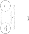
Figure 2 illustrates another embodiment of the Fsw control process implemented by theDFC circuitry 110 included in or associated with themultiphase VR controller 102. According to this embodiment, theDFC circuitry 110 can change the switching frequency Fsw between Fsw0 and Fsw1 based on phase current information provided by thecurrent balance circuitry 114. Thecurrent balance circuitry 114 can include any standard circuitry for sensing and/or measuring the phase currents and the output voltage Vout of the system. Thecontroller 102 also uses the phase current and output voltage feedback information to adjust the duty cycle of the PWM control signals input to thephases 100. - If the absolute difference between two sensed/measured phase currents (e.g. iph1 and iph2 in
Figure 2 ) exceeds a threshold value thr for longer than a defined time interval Nfsw1, theDFC circuitry 110 changes the switching frequency Fsw from the base value Fsw0 to Fsw1 or from Fsw1 back to the base value Fsw0, depending on which value Fsw is set at when the phase current threshold condition is satisfied. This way, thecontroller 102 can respond to dynamic load frequency changes by making corresponding adjustments to the switching frequency Fsw. In one embodiment, the threshold value thr and the defined time interval Nfsw1 are selected so that theDFC circuitry 110 can change the switching frequency Fsw from Fsw0 (or Fswi) to Fsw1 (or Fsw0) before the peak current limit of the inductors is exceeded. In another embodiment, theDFC circuitry 110 determines Fsw1 from a lookup table (LUT) 116 e.g. based on peak current which determines which Fsw value to select (e.g. higher peak current, lower Fsw change and vice-versa). In yet another embodiment, theDFC circuitry 110 determines Fsw1 based on a formula f(x) 118 programmed into thecontroller 102. For example, peak current and the present value of Fsw (Fswo or Fswi) can be input to a logic block which implements the formula f(x) 118 to determine the amount of Fsw adjustment (increase/decrease). - As mentioned above, the
DFC circuitry 110 included in or associated with themultiphase VR controller 102 can likewise change the switching frequency Fsw from Fsw1 back to the base value Fsw0 if the frequency Fload at which the load current iL changes repetitively moves to within a predetermined range of Fsw1. This way, Fsw can move back and forth between Fsw0 and Fsw1 in response to the dynamic load transient frequency Fload, to avoid oscillations that fall within the bandwidth of the control loop where loop gain is high. When the dynamic load transient condition goes away, the trigger mechanism to move back to the base Fsw0 value can be error voltage. For example, if the error voltage is less than a certain value (e.g. by checking a comparator), then no dynamic load transient condition is present and therefore no aliasing should occur at the base value Fsw0, and theDFC circuitry 110 can change the switching frequency Fsw back to Fsw0. In another embodiment, thecontroller 102 can monitor Fload. If Fload decreases sufficiently, then no dynamic load transient condition is present and theDFC circuitry 110 can change the switching frequency Fsw back to the base value Fsw0. - The ability to move Fsw away from the base value Fsw0 can be disabled under certain conditions. For example, the
DFC circuitry 110 may be prevented from changing Fsw in the following VR states: non-active states e.g. during start up and shutdown; DVID transition states (transitioning from one target voltage to another); during single phase regulation when only onephase 100 is used to regulate theload 104; and/or during dynamic phasing add/drop when one ormore phases 100 are being added or dropped from regulation. - By changing Fsw in response to Fload in a multiphase VR system whose Fsw is otherwise fixed, the oscillations that do arise fall outside the bandwidth of the control loop where loop gain is low, reducing or eliminating aliasing effects on the phase currents. The
DFC circuitry 110 can also change the switching frequency Fsw from Fsw1 back to the base value Fsw0 after detecting no dynamic load transients over a defined time interval Nfsw2. The defined time intervals Nfsw1 and Nfsw2 are design choices, and can be permanently set or programmable so as to avoid changing Fsw more often than warranted. - In general, the value of Fsw1 depends on the bandwidth of the
controller 102, which is also a design parameter. Hence, any Fsw1 which avoids aliasing affects when Fload is at or near the base value Fsw0 or ½ Fsw0 can be used and within the scope of the embodiments described herein. -
Figure 3A plots output voltage Vout and phase currents iph1 and iph2 for three different load frequency (Fload) examples: 190 kHz, 270 kHz and 520 kHz. The multiphase voltage regulator system initially operates at a switching frequency Fsw of 520 kHz and the dynamic load transient frequency Fload is initially at 190 kHz in this example. The load and switching frequencies discussed herein are merely for illustrative purposes, and should not be considered limiting in any way. Since any oscillations which occur at the difference between 520 kHz and 190 kHz fall outside the bandwidth of thecontroller 102, theDFC circuitry 110 does not change Fsw. That is, Fsw remains fixed at 520 kHz. - However, as Fload increases from 190 kHz to near Fsw, oscillations will fall within the bandwidth of the
controller 102, and due to higher loop gain, cause aliasing effects and thus imbalance in the phase currents if unmitigated. The middle part ofFigure 3A shows the dynamic load transient frequency Fload at 270 kHz. At this frequency, the oscillations become more prominent since loop gain is higher at the frequency delta of 520 kHz - 270 kHz compared to 520kHz - 190kHz. However, Fsw need not necessarily be moved away from Fload at this point since the loop gain is still sufficiently low at that oscilation frequency. The righthand part ofFigure 3A shows the dynamic load transient frequency Fload at 520 kHz, which equals Fsw in this example. If unmitigated, significant aliasing effects would occur under these conditions, since the oscillations are subject to high loop gain. - To avoid aliasing effects on the phase currents, the
DFC circuitry 110 changes the switching frequency Fsw from 520 kHz to a different value sufficiently away from Fload to avoid or at least meaningfully reduce aliasing effects. For example, Fsw is moved to 640 kHz. By moving Fsw away from Fload by a sufficient margin, oscillations again fall outside the bandwidth of thecontroller 102 where loop gain is relatively low and the multiphase VR system experiences no meaningful or at least tolerable aliasing effects. Contrast this withFigure 3B , which shows the same Fsw and Fload examples described above, except without intervention by theDFC circuitry 110. As can be seen in the righthand part ofFigure 3B , circulating current resulting from aliasing leads to significant phase current imbalance. -
Figure 4A graphs the output voltage Vout and phase currents iph1 and iph2 for the same dynamic load transient frequency Fload examples inFigures 3A and 3B : 190 kHz, 270 kHz and 520 kHz. Different in this example, the multiphase VR system initially operates at a switching frequency Fsw of 520 kHz and the dynamic load transient frequency Fload also is at 520 kHz. To avoid aliasing effects, theDFC circuitry 110 changes the switching frequency Fsw from 520 kHz to a different value sufficiently away from Fload to avoid or at least meaningfully reduce aliasing effects. For example, Fsw is moved to 640 kHz. Again, by moving Fsw away from Fload by a sufficient margin, oscillations fall outside the bandwidth of thecontroller 102 where loop gain is relatively low and the multiphase VR system experiences no meaningful or at least tolerable aliasing effects. Contrast this withFigure 4B , which shows the same Fsw and Fload examples asFigure 4A , except without intervention by theDFC circuitry 110. As can be seen in the left-hand part ofFigure 4B , circulating current resulting from aliasing leads to significant phase current imbalance. - As mentioned above in connection with
Figures 3A and 3B , the load and switching frequencies Fload and Fsw examples shown inFigures 4A and 4B are provided merely for illustrative purposes and should not be considered limiting in any way. However, VR system efficiency tends to drop at frequencies above the base value Fsw0, so Fsw is preferably changed as little as possible while still avoiding or meaningfully reducing aliasing effects and without unduly/overly reducing VR system efficiency. -
Figure 5 illustrates themultiphase VR controller 102 in more detail, and an embodiment of thecurrent balance circuitry 114 included in or associated with thecontroller 102. According to this embodiment, thecontroller 102 includes voltage sense (VS)circuitry 200 for sensing/measuring the regulator output voltage Vout. A voltage sense ADC (analog to digital converter) 202 converts an analog error voltage (Verr) i.e. the difference between sensed/measured Vout and a target voltage (Vtgt), into a digital representation. A PID (proportional-integral-derivative)compensator 204 implements a compensator transfer function with the digital error voltage as an input and duty cycle as the output. ThePWM circuitry 112 of thecontroller 102 includes a multiphasedigital PWM 206 that sets the gain for thedifferent phases 102 based on the output of thePID compensator 204 and current balance information (Ibal) from thecurrent balance circuitry 114, and converts the digital duty cycle information into a pulse width modulated waveform (PMWN) that interfaces with thedriver 108 to control the on/off states of the switch devices HS, LS of the respective phases 102. - The
current balance circuitry 114 includes current sense andADC circuitry 208 for monitoring the individual phase currents (Iph1, Iph2, ..., IphN) of the N phases 100, and for converting the monitored phase currents into corresponding digital phase current information which is processed by respective channel current PI (proportional-integral)circuitry 210 for eachphase 102 of the VR system. Thecurrent balance circuitry 114 also includes an averagingcircuit 212 for calculating the average phase current Iph_avg. Thecurrent balance circuitry 114 converts the phase current information from the channelcurrent PI circuitry 210 into current balance information (Ibal) which represents corresponding adjustments to the duty cycle of eachindividual phase 102, to adjust the phase currents so they remain balanced. - The
current balance circuitry 114 adjusts the PWM duty cycle of eachindividual phase 102 to increase or decrease the corresponding phase current relative to the other phases 102. This is typically done by a filter with the transfer function:
Xth phase 102, Iphx is the measured current of theXth phase 102, Itargx is the target current for theXth phase 102, and Ki_ibal and Kp_ibal are integral and proportional gains, respectively, input to the respective channelcurrent PI circuitry 210. Thecurrent balance circuitry 114 adjusts individual phase currents to match a certain allocation as determined by thecontroller 102 for the total load current, between active ones of thephases 102. - The
DFC circuitry 110 included in or associated with themultiphase VR controller 102 is in communication with thecurrent balance circuitry 114, so that theDFC circuitry 110 can change the switching frequency Fsw from Fsw0 to Fsw1 (or vice-versa) if the frequency Fload at which the load current iL changes repetitively is within a predetermined range of Fsw0 (or Fsw1), as indicated by the absolute different between two phase currents as previously described herein and shown inFigure 2 . This way, oscillations that fall within the bandwidth of the control loop where loop gain is high can be avoided, by making corresponding adjustments to Fsw based on phase current behaviour. - The
controller 102 can implement new registers for the phase current-based Fsw adjustment approach. For example, a first register can store the value Fsw1, a second register can store Nfsw1 and Nfsw2, a third register can store a phase current imbalance threshold, a fourth register can store a blanking time imposed after a Fsw frequency hop (change), and fifth register can store an apc (amps per code) delta for Fsw1. - In addition or alternatively, the
DFC circuitry 110 included in or associated with themultiphase VR controller 102 can adjust Fsw to avoid oscillations that fall within the bandwidth of the control loop based on Fload measurements. In one embodiment, thecontroller 102 measures the frequency Fload at which the load current changes and theDFC circuitry 110 changes the switching frequency Fsw from Fsw0 to Fsw1 (or vice-versa) if the difference between the measured frequency of the load current and Fsw0 (of Fsw1) is within the bandwidth of thecontroller 102. For example, thecontroller 102 can measure the rate of change of the output voltage Vout of the multiphase VR system (e.g. via a counter) and convert the measured rate of change to a frequency indicative of the frequency Fload at which the load current changes. In another embodiment, thecontroller 102 includes active transient response (ATR) circuitry for detecting and responding to transient conditions at theload 104. If frequency (FATR) of a detected transient load condition is within the range of ½ Fsw±x or Fsw±y, theDFC circuitry 110 can change Fsw0 to Fsw1 (or vice-versa). If FATR does not fall within one of those regions, theDFC circuitry 110 can change Fsw back to the base value Fsw0. The parameters x, y, Fsw0 and Fsw1 can be programmable parameters set by the user. - In addition or alternatively, the
DFC circuitry 110 included in or associated with themultiphase VR controller 102 can adjust Fsw to avoid oscillations that fall within the bandwidth of the control loop based on direct measurements of the phase current imbalance frequency. In one embodiment, thecontroller 102 determines the phase current imbalance frequency based on phase current measurements taken for the plurality ofphases 100 and theDFC circuitry 110 changes the switching frequency Fsw from Fsw0 to Fsw1 (or vice-versa) if the measured phase current imbalance frequency is lower than a threshold frequency. -
Figure 6 illustrates the effect of changing the switching frequency Fsw based on the dynamic load transient frequency Fload. In this example, the Fload is 520 kHz. The peak current (Ipeak), the peak-to-peak phase current difference (Iph(pk-pk)) and half ripple current (1/2 ripple) are plotted as a function of Fsw and Fload. The peak current Ipeak and the peak-to-peak phase current difference Iph(pk-pk) spike when Fsw = Fload. By moving Fsw away from Fload as described herein, both Ipeak and Iph(pk-pk) drop significantly. In the example shown, the peak-to-peak phase current difference Iph(pk-pk) decreases by about 30A when Fload is 520 kHz and Fsw is moved from Fsw0 = 520 kHz to Fsw1 = 400 kHz, and decreases by about 60A by instead moving Fsw from Fsw0 = 520 kHz to Fsw1 = 800 kHz. However, Fsw values above the base value Fsw0 decrease the VR system efficiency, so efficiency is a trade-off with peak current and peak-to-peak phase current performance. Ripple current also improves (decreases) with higher Fsw. - Terms such as "first", "second", and the like, are used to describe various elements, regions, sections, etc. and are also not intended to be limiting. Like terms refer to like elements throughout the description.
- As used herein, the terms "having", "containing", "including", "comprising" and the like are open ended terms that indicate the presence of stated elements or features, but do not preclude additional elements or features. The articles "a", "an" and "the" are intended to include the plural as well as the singular, unless the context clearly indicates otherwise.
- It is to be understood that the features of the various embodiments described herein may be combined with each other, unless specifically noted otherwise.
Claims (20)
- A multiphase voltage regulator, comprising:a plurality of phases, each phase configured to output a phase current to a load through an inductor in response to a control signal input to the phase; anda controller operable to:generate the control signals input to the phases;set a switching frequency of the control signals to a first value; andchange the switching frequency from the first value to a second value different than the first value if the load current changes repetitively at a frequency that is within a predetermined range of the first value of the switching frequency.
- The multiphase voltage regulator of claim 1, wherein the controller is operable to adjust a duty cycle of one or more of the control signals to balance the phase currents, and change the switching frequency from the first value to the second value if the phase currents cannot be balanced without exceeding a peak current limit of the inductors.
- The multiphase voltage regulator of claim 1, or 2 wherein the controller is operable to change the switching frequency from the first value to the second value if the difference between two of the phase currents exceeds a threshold value for longer than a defined time interval.
- The multiphase voltage regulator of claim 3, wherein the threshold value and the defined time interval are selected so that the controller is operable to change the switching frequency from the first value to the second value before a peak current limit of the inductors is exceeded.
- The multiphase voltage regulator of any one of claims 1 to 4, wherein the controller is operable to determine the second value from a lookup table or based on a formula programmed into the controller.
- The multiphase voltage regulator of any one of claims 1 to 5, wherein the controller is operable to measure the frequency at which the load current changes, and change the switching frequency from the first value to the second value if the difference between the measured frequency of the load current and the first value is within a bandwidth of the controller.
- The multiphase voltage regulator of claim 6, wherein the controller is operable to measure the rate of change of an output voltage of the multiphase voltage regulator and convert the measured rate of change to a frequency indicative of the frequency at which the load current changes.
- The multiphase voltage regulator of any one of claims 1 to 7, wherein the controller is operable to determine a phase current imbalance frequency based on phase current measurements taken for the plurality of phases, and change the switching frequency from the first value to the second value if the measured phase current imbalance frequency is lower than a threshold frequency.
- The multiphase voltage regulator of any one of claims 1 to 8, wherein the controller is operable to change the switching frequency from the second value back to the first value if the frequency at which the load current changes repetitively moves to within a predetermined range of the second value of the switching frequency.
- The multiphase voltage regulator of any one of claims 1 to 8, wherein the controller is operable to change the switching frequency from the second value back to the first value after detecting no dynamic load transients over a defined time interval.
- A method of operating a multiphase voltage regulator that has a plurality of phases, each phase configured to output a phase current to a load through an inductor in response to a control signal input to the phase, the method comprising:setting a switching frequency of the control signals to a first value; andchanging the switching frequency from the first value to a second value different than the first value if the load current changes repetitively at a frequency that is within a predetermined range of the first value of the switching frequency.
- The method of claim 11, wherein changing the switching frequency from the first value to the second value comprises:adjusting a duty cycle of one or more of the control signals to balance the phase currents; andchanging the switching frequency from the first value to the second value if the phase currents cannot be balanced without exceeding a peak current limit of the inductors.
- The method of claim 11 or 12, wherein changing the switching frequency from the first value to the second value comprises:measuring the phase currents; andchanging the switching frequency from the first value to the second value if the difference between two of the phase currents exceeds a threshold value for longer than a defined time interval.
- The method of claim 13, further comprising:selecting the threshold value and the defined time interval so that the switching frequency changes from the first value to the second value before a peak current limit of the inductors is exceeded.
- The method of any one of claims 11 to 14, further comprising:determining the second value from a lookup table or based on a formula programmed into a controller of the multiphase voltage regulator.
- The method of any one of claims 11 to 15, wherein changing the switching frequency from the first value to the second value comprises:measuring the frequency at which the load current changes; andchanging the switching frequency from the first value to the second value if the difference between the measured frequency of the load current and the first value is within a bandwidth of a controller of the multiphase voltage regulator.
- The method of claim 16, wherein measuring the frequency at which the load current changes comprises:measuring the rate of change of an output voltage of the multiphase voltage regulator; andconverting the measured rate of change to frequency.
- The method of any one of claims 11 to 17, wherein changing the switching frequency from the first value to the second value comprises:determining a phase current imbalance frequency based on phase current measurements taken for the plurality of phases; andchanging the switching frequency from the first value to the second value if the measured phase current imbalance frequency is lower than a threshold frequency.
- The method of any one of claims 11 to 18, further comprising:changing the switching frequency from the second value back to the first value if the frequency at which the load current changes repetitively moves to within a predetermined range of the second value of the switching frequency.
- The method of any one of claims 11 to 18, further comprising:changing the switching frequency from the second value back to the first value after detecting no dynamic load transients over a defined time interval.
Applications Claiming Priority (1)
| Application Number | Priority Date | Filing Date | Title |
|---|---|---|---|
| US15/729,170 US10324480B2 (en) | 2017-10-10 | 2017-10-10 | Dynamic switching frequency control in multiphase voltage regulators |
Publications (2)
| Publication Number | Publication Date |
|---|---|
| EP3471256A1 true EP3471256A1 (en) | 2019-04-17 |
| EP3471256B1 EP3471256B1 (en) | 2022-07-20 |
Family
ID=63798858
Family Applications (1)
| Application Number | Title | Priority Date | Filing Date |
|---|---|---|---|
| EP18199218.1A Active EP3471256B1 (en) | 2017-10-10 | 2018-10-09 | Dynamic switching frequency control in multiphase voltage regulators |
Country Status (3)
| Country | Link |
|---|---|
| US (1) | US10324480B2 (en) |
| EP (1) | EP3471256B1 (en) |
| CN (1) | CN109660123B (en) |
Families Citing this family (3)
| Publication number | Priority date | Publication date | Assignee | Title |
|---|---|---|---|---|
| CN110224592B (en) | 2019-06-13 | 2021-08-13 | 南京矽力微电子技术有限公司 | Multiphase critical conduction power converter and control method thereof |
| US11340680B2 (en) * | 2020-07-02 | 2022-05-24 | Hewlett Packard Enterprise Development Lp | System controller for monitoring a characteristic system energy of a computing system |
| US11860660B2 (en) * | 2021-06-02 | 2024-01-02 | Mediatek Singapore Pte. Ltd. | Apparatus and method of performing load transient frequency detection for dynamically managing controllable circuit in voltage regulator |
Citations (3)
| Publication number | Priority date | Publication date | Assignee | Title |
|---|---|---|---|---|
| US20090309564A1 (en) * | 2008-06-13 | 2009-12-17 | Stmicroelectronics S.R.L. | Method for controlling a voltage regulator, in particular a converter of the multiphase interleaving type and corresponding controller |
| US20110133704A1 (en) * | 2009-06-10 | 2011-06-09 | Stmicroelectronics S.R.I | Method for controlling an interleaving multiphase regulator and corresponding system |
| US20160233766A1 (en) * | 2015-02-05 | 2016-08-11 | Infineon Technologies Austria Ag | Multi-phase switching voltage regulator having asymmetric phase inductance |
Family Cites Families (9)
| Publication number | Priority date | Publication date | Assignee | Title |
|---|---|---|---|---|
| US3419818A (en) * | 1965-05-20 | 1968-12-31 | Gen Motors Corp | Pulse frequency and pulse width control for a modulator |
| US7944191B2 (en) * | 2005-10-14 | 2011-05-17 | Monolithic Power Systems, Inc. | Switching regulator with automatic multi mode conversion |
| US8618788B2 (en) * | 2007-03-30 | 2013-12-31 | Malay Trivedi | Dynamically adjusted multi-phase regulator |
| US8259477B2 (en) * | 2007-05-30 | 2012-09-04 | The Regents Of The University Of California | Multiphase resonant converter for DC-DC applications |
| US7932704B1 (en) * | 2008-02-01 | 2011-04-26 | Intersil Americas Inc. | System and method of providing control pulses to control operation of a converter with high frequency repetitive load transients |
| CN101345491B (en) * | 2008-05-30 | 2011-01-19 | 华硕电脑股份有限公司 | Frequency conversion multi-phase voltage regulator and its control method |
| EP2673871B1 (en) * | 2011-02-10 | 2015-11-04 | PAI Capital LLC | Digital phase adjustment for multi-phase power converters |
| US8994346B2 (en) * | 2012-02-09 | 2015-03-31 | Dell Products Lp | Systems and methods for dynamic management of switching frequency for voltage regulation |
| US9240721B2 (en) * | 2012-07-12 | 2016-01-19 | Infineon Technologies Austria Ag | Multiphase digital current mode controller with dynamic current allocation |
-
2017
- 2017-10-10 US US15/729,170 patent/US10324480B2/en active Active
-
2018
- 2018-10-09 EP EP18199218.1A patent/EP3471256B1/en active Active
- 2018-10-10 CN CN201811180341.6A patent/CN109660123B/en active Active
Patent Citations (3)
| Publication number | Priority date | Publication date | Assignee | Title |
|---|---|---|---|---|
| US20090309564A1 (en) * | 2008-06-13 | 2009-12-17 | Stmicroelectronics S.R.L. | Method for controlling a voltage regulator, in particular a converter of the multiphase interleaving type and corresponding controller |
| US20110133704A1 (en) * | 2009-06-10 | 2011-06-09 | Stmicroelectronics S.R.I | Method for controlling an interleaving multiphase regulator and corresponding system |
| US20160233766A1 (en) * | 2015-02-05 | 2016-08-11 | Infineon Technologies Austria Ag | Multi-phase switching voltage regulator having asymmetric phase inductance |
Also Published As
| Publication number | Publication date |
|---|---|
| US20190107853A1 (en) | 2019-04-11 |
| EP3471256B1 (en) | 2022-07-20 |
| US10324480B2 (en) | 2019-06-18 |
| CN109660123A (en) | 2019-04-19 |
| CN109660123B (en) | 2023-10-27 |
Similar Documents
| Publication | Publication Date | Title |
|---|---|---|
| KR101788441B1 (en) | Multi-phase switching voltage regulator having asymmetric phase | |
| US10666142B2 (en) | Switching converter using pulse-width modulation and current-mode control | |
| US8232782B2 (en) | System and method for equalizing the small signal response of variable phase voltage regulators | |
| US8487593B2 (en) | System and method for detection and compensation of aggressive output filters for switched mode power supplies | |
| US8581565B2 (en) | DC-to-DC converter having secondary-side digital sensing and control | |
| US20140125306A1 (en) | Switching Regulator Control with Nonlinear Feed-Forward Correction | |
| EP2885861B1 (en) | A current-mode controller for step-down (buck) converter | |
| EP3471256B1 (en) | Dynamic switching frequency control in multiphase voltage regulators | |
| US9998008B2 (en) | Active transient response for DC-DC converters | |
| US11557967B2 (en) | Voltage regulator with adaptive feed-forward compensation for periodic loads | |
| JP2006136190A (en) | Regulator, method and circuit for controlling it, and method of adjusting voltage impressed to load terminal | |
| KR20070056068A (en) | Dc-dc converter with adaptive switching parameter adjustment | |
| US8476880B2 (en) | System and method for reducing output voltage of a power regulator under light load | |
| JP2000227808A (en) | Dc-dc converter provided with inductor current detector and its adjusting method | |
| US20070236192A1 (en) | Adaptive DC to DC Converter System | |
| US10778101B1 (en) | Switching regulator controller configuration parameter optimization | |
| US7688050B2 (en) | Switching power supply controller with unidirectional transient gain change | |
| US20230231477A1 (en) | Power supply controller | |
| US10651743B2 (en) | Control loop parameter setting in a voltage regulator controller | |
| US20070236196A1 (en) | Adaptive DC to DC converter system | |
| US7557552B2 (en) | Adaptive DC to DC converter system using a combination of duty cycle and slew rate modulations | |
| US20160270172A1 (en) | Switch Mode Power Supplies, Control Arrangements therefor and Methods of Operating thereof | |
| US11081957B2 (en) | Power converter with multi-mode timing control | |
| US10284077B1 (en) | PFC controller providing reduced line current slope when in burst mode | |
| KR100593455B1 (en) | Switching control method and input current limit control device of boost type chopper |
Legal Events
| Date | Code | Title | Description |
|---|---|---|---|
| PUAI | Public reference made under article 153(3) epc to a published international application that has entered the european phase |
Free format text: ORIGINAL CODE: 0009012 |
|
| STAA | Information on the status of an ep patent application or granted ep patent |
Free format text: STATUS: THE APPLICATION HAS BEEN PUBLISHED |
|
| AK | Designated contracting states |
Kind code of ref document: A1 Designated state(s): AL AT BE BG CH CY CZ DE DK EE ES FI FR GB GR HR HU IE IS IT LI LT LU LV MC MK MT NL NO PL PT RO RS SE SI SK SM TR |
|
| AX | Request for extension of the european patent |
Extension state: BA ME |
|
| STAA | Information on the status of an ep patent application or granted ep patent |
Free format text: STATUS: REQUEST FOR EXAMINATION WAS MADE |
|
| 17P | Request for examination filed |
Effective date: 20191017 |
|
| RBV | Designated contracting states (corrected) |
Designated state(s): AL AT BE BG CH CY CZ DE DK EE ES FI FR GB GR HR HU IE IS IT LI LT LU LV MC MK MT NL NO PL PT RO RS SE SI SK SM TR |
|
| STAA | Information on the status of an ep patent application or granted ep patent |
Free format text: STATUS: EXAMINATION IS IN PROGRESS |
|
| STAA | Information on the status of an ep patent application or granted ep patent |
Free format text: STATUS: EXAMINATION IS IN PROGRESS |
|
| 17Q | First examination report despatched |
Effective date: 20210111 |
|
| STAA | Information on the status of an ep patent application or granted ep patent |
Free format text: STATUS: EXAMINATION IS IN PROGRESS |
|
| GRAP | Despatch of communication of intention to grant a patent |
Free format text: ORIGINAL CODE: EPIDOSNIGR1 |
|
| STAA | Information on the status of an ep patent application or granted ep patent |
Free format text: STATUS: GRANT OF PATENT IS INTENDED |
|
| RIC1 | Information provided on ipc code assigned before grant |
Ipc: G05F 1/10 20060101ALI20220116BHEP Ipc: H02M 3/158 20060101AFI20220116BHEP |
|
| INTG | Intention to grant announced |
Effective date: 20220201 |
|
| GRAS | Grant fee paid |
Free format text: ORIGINAL CODE: EPIDOSNIGR3 |
|
| GRAA | (expected) grant |
Free format text: ORIGINAL CODE: 0009210 |
|
| STAA | Information on the status of an ep patent application or granted ep patent |
Free format text: STATUS: THE PATENT HAS BEEN GRANTED |
|
| AK | Designated contracting states |
Kind code of ref document: B1 Designated state(s): AL AT BE BG CH CY CZ DE DK EE ES FI FR GB GR HR HU IE IS IT LI LT LU LV MC MK MT NL NO PL PT RO RS SE SI SK SM TR |
|
| REG | Reference to a national code |
Ref country code: CH Ref legal event code: EP |
|
| REG | Reference to a national code |
Ref country code: DE Ref legal event code: R096 Ref document number: 602018038069 Country of ref document: DE |
|
| REG | Reference to a national code |
Ref country code: AT Ref legal event code: REF Ref document number: 1506199 Country of ref document: AT Kind code of ref document: T Effective date: 20220815 |
|
| REG | Reference to a national code |
Ref country code: IE Ref legal event code: FG4D |
|
| REG | Reference to a national code |
Ref country code: LT Ref legal event code: MG9D |
|
| REG | Reference to a national code |
Ref country code: NL Ref legal event code: MP Effective date: 20220720 |
|
| PG25 | Lapsed in a contracting state [announced via postgrant information from national office to epo] |
Ref country code: SE Free format text: LAPSE BECAUSE OF FAILURE TO SUBMIT A TRANSLATION OF THE DESCRIPTION OR TO PAY THE FEE WITHIN THE PRESCRIBED TIME-LIMIT Effective date: 20220720 Ref country code: RS Free format text: LAPSE BECAUSE OF FAILURE TO SUBMIT A TRANSLATION OF THE DESCRIPTION OR TO PAY THE FEE WITHIN THE PRESCRIBED TIME-LIMIT Effective date: 20220720 Ref country code: PT Free format text: LAPSE BECAUSE OF FAILURE TO SUBMIT A TRANSLATION OF THE DESCRIPTION OR TO PAY THE FEE WITHIN THE PRESCRIBED TIME-LIMIT Effective date: 20221121 Ref country code: NO Free format text: LAPSE BECAUSE OF FAILURE TO SUBMIT A TRANSLATION OF THE DESCRIPTION OR TO PAY THE FEE WITHIN THE PRESCRIBED TIME-LIMIT Effective date: 20221020 Ref country code: NL Free format text: LAPSE BECAUSE OF FAILURE TO SUBMIT A TRANSLATION OF THE DESCRIPTION OR TO PAY THE FEE WITHIN THE PRESCRIBED TIME-LIMIT Effective date: 20220720 Ref country code: LV Free format text: LAPSE BECAUSE OF FAILURE TO SUBMIT A TRANSLATION OF THE DESCRIPTION OR TO PAY THE FEE WITHIN THE PRESCRIBED TIME-LIMIT Effective date: 20220720 Ref country code: LT Free format text: LAPSE BECAUSE OF FAILURE TO SUBMIT A TRANSLATION OF THE DESCRIPTION OR TO PAY THE FEE WITHIN THE PRESCRIBED TIME-LIMIT Effective date: 20220720 Ref country code: FI Free format text: LAPSE BECAUSE OF FAILURE TO SUBMIT A TRANSLATION OF THE DESCRIPTION OR TO PAY THE FEE WITHIN THE PRESCRIBED TIME-LIMIT Effective date: 20220720 Ref country code: ES Free format text: LAPSE BECAUSE OF FAILURE TO SUBMIT A TRANSLATION OF THE DESCRIPTION OR TO PAY THE FEE WITHIN THE PRESCRIBED TIME-LIMIT Effective date: 20220720 |
|
| REG | Reference to a national code |
Ref country code: AT Ref legal event code: MK05 Ref document number: 1506199 Country of ref document: AT Kind code of ref document: T Effective date: 20220720 |
|
| PG25 | Lapsed in a contracting state [announced via postgrant information from national office to epo] |
Ref country code: PL Free format text: LAPSE BECAUSE OF FAILURE TO SUBMIT A TRANSLATION OF THE DESCRIPTION OR TO PAY THE FEE WITHIN THE PRESCRIBED TIME-LIMIT Effective date: 20220720 Ref country code: IS Free format text: LAPSE BECAUSE OF FAILURE TO SUBMIT A TRANSLATION OF THE DESCRIPTION OR TO PAY THE FEE WITHIN THE PRESCRIBED TIME-LIMIT Effective date: 20221120 Ref country code: HR Free format text: LAPSE BECAUSE OF FAILURE TO SUBMIT A TRANSLATION OF THE DESCRIPTION OR TO PAY THE FEE WITHIN THE PRESCRIBED TIME-LIMIT Effective date: 20220720 Ref country code: GR Free format text: LAPSE BECAUSE OF FAILURE TO SUBMIT A TRANSLATION OF THE DESCRIPTION OR TO PAY THE FEE WITHIN THE PRESCRIBED TIME-LIMIT Effective date: 20221021 |
|
| REG | Reference to a national code |
Ref country code: DE Ref legal event code: R097 Ref document number: 602018038069 Country of ref document: DE |
|
| PG25 | Lapsed in a contracting state [announced via postgrant information from national office to epo] |
Ref country code: SM Free format text: LAPSE BECAUSE OF FAILURE TO SUBMIT A TRANSLATION OF THE DESCRIPTION OR TO PAY THE FEE WITHIN THE PRESCRIBED TIME-LIMIT Effective date: 20220720 Ref country code: RO Free format text: LAPSE BECAUSE OF FAILURE TO SUBMIT A TRANSLATION OF THE DESCRIPTION OR TO PAY THE FEE WITHIN THE PRESCRIBED TIME-LIMIT Effective date: 20220720 Ref country code: DK Free format text: LAPSE BECAUSE OF FAILURE TO SUBMIT A TRANSLATION OF THE DESCRIPTION OR TO PAY THE FEE WITHIN THE PRESCRIBED TIME-LIMIT Effective date: 20220720 Ref country code: CZ Free format text: LAPSE BECAUSE OF FAILURE TO SUBMIT A TRANSLATION OF THE DESCRIPTION OR TO PAY THE FEE WITHIN THE PRESCRIBED TIME-LIMIT Effective date: 20220720 Ref country code: AT Free format text: LAPSE BECAUSE OF FAILURE TO SUBMIT A TRANSLATION OF THE DESCRIPTION OR TO PAY THE FEE WITHIN THE PRESCRIBED TIME-LIMIT Effective date: 20220720 |
|
| PLBE | No opposition filed within time limit |
Free format text: ORIGINAL CODE: 0009261 |
|
| STAA | Information on the status of an ep patent application or granted ep patent |
Free format text: STATUS: NO OPPOSITION FILED WITHIN TIME LIMIT |
|
| PG25 | Lapsed in a contracting state [announced via postgrant information from national office to epo] |
Ref country code: SK Free format text: LAPSE BECAUSE OF FAILURE TO SUBMIT A TRANSLATION OF THE DESCRIPTION OR TO PAY THE FEE WITHIN THE PRESCRIBED TIME-LIMIT Effective date: 20220720 Ref country code: MC Free format text: LAPSE BECAUSE OF FAILURE TO SUBMIT A TRANSLATION OF THE DESCRIPTION OR TO PAY THE FEE WITHIN THE PRESCRIBED TIME-LIMIT Effective date: 20220720 Ref country code: EE Free format text: LAPSE BECAUSE OF FAILURE TO SUBMIT A TRANSLATION OF THE DESCRIPTION OR TO PAY THE FEE WITHIN THE PRESCRIBED TIME-LIMIT Effective date: 20220720 |
|
| REG | Reference to a national code |
Ref country code: CH Ref legal event code: PL |
|
| REG | Reference to a national code |
Ref country code: BE Ref legal event code: MM Effective date: 20221031 |
|
| 26N | No opposition filed |
Effective date: 20230421 |
|
| PG25 | Lapsed in a contracting state [announced via postgrant information from national office to epo] |
Ref country code: LU Free format text: LAPSE BECAUSE OF NON-PAYMENT OF DUE FEES Effective date: 20221009 Ref country code: AL Free format text: LAPSE BECAUSE OF FAILURE TO SUBMIT A TRANSLATION OF THE DESCRIPTION OR TO PAY THE FEE WITHIN THE PRESCRIBED TIME-LIMIT Effective date: 20220720 |
|
| P01 | Opt-out of the competence of the unified patent court (upc) registered |
Effective date: 20230528 |
|
| PG25 | Lapsed in a contracting state [announced via postgrant information from national office to epo] |
Ref country code: LI Free format text: LAPSE BECAUSE OF NON-PAYMENT OF DUE FEES Effective date: 20221031 Ref country code: CH Free format text: LAPSE BECAUSE OF NON-PAYMENT OF DUE FEES Effective date: 20221031 |
|
| PG25 | Lapsed in a contracting state [announced via postgrant information from national office to epo] |
Ref country code: SI Free format text: LAPSE BECAUSE OF FAILURE TO SUBMIT A TRANSLATION OF THE DESCRIPTION OR TO PAY THE FEE WITHIN THE PRESCRIBED TIME-LIMIT Effective date: 20220720 |
|
| PG25 | Lapsed in a contracting state [announced via postgrant information from national office to epo] |
Ref country code: BE Free format text: LAPSE BECAUSE OF NON-PAYMENT OF DUE FEES Effective date: 20221031 |
|
| PG25 | Lapsed in a contracting state [announced via postgrant information from national office to epo] |
Ref country code: IE Free format text: LAPSE BECAUSE OF NON-PAYMENT OF DUE FEES Effective date: 20221009 |
|
| PGFP | Annual fee paid to national office [announced via postgrant information from national office to epo] |
Ref country code: GB Payment date: 20231020 Year of fee payment: 6 |
|
| PGFP | Annual fee paid to national office [announced via postgrant information from national office to epo] |
Ref country code: FR Payment date: 20231026 Year of fee payment: 6 Ref country code: DE Payment date: 20231218 Year of fee payment: 6 |
|
| PG25 | Lapsed in a contracting state [announced via postgrant information from national office to epo] |
Ref country code: HU Free format text: LAPSE BECAUSE OF FAILURE TO SUBMIT A TRANSLATION OF THE DESCRIPTION OR TO PAY THE FEE WITHIN THE PRESCRIBED TIME-LIMIT; INVALID AB INITIO Effective date: 20181009 |