EP3471250A1 - Voltage conversion device and leakage inductance determination method - Google Patents
Voltage conversion device and leakage inductance determination method Download PDFInfo
- Publication number
- EP3471250A1 EP3471250A1 EP17810133.3A EP17810133A EP3471250A1 EP 3471250 A1 EP3471250 A1 EP 3471250A1 EP 17810133 A EP17810133 A EP 17810133A EP 3471250 A1 EP3471250 A1 EP 3471250A1
- Authority
- EP
- European Patent Office
- Prior art keywords
- inductors
- leakage inductance
- ripple current
- voltage conversion
- reduction rate
- Prior art date
- Legal status (The legal status is an assumption and is not a legal conclusion. Google has not performed a legal analysis and makes no representation as to the accuracy of the status listed.)
- Withdrawn
Links
Images















Classifications
-
- H—ELECTRICITY
- H01—ELECTRIC ELEMENTS
- H01F—MAGNETS; INDUCTANCES; TRANSFORMERS; SELECTION OF MATERIALS FOR THEIR MAGNETIC PROPERTIES
- H01F27/00—Details of transformers or inductances, in general
- H01F27/28—Coils; Windings; Conductive connections
-
- H—ELECTRICITY
- H02—GENERATION; CONVERSION OR DISTRIBUTION OF ELECTRIC POWER
- H02M—APPARATUS FOR CONVERSION BETWEEN AC AND AC, BETWEEN AC AND DC, OR BETWEEN DC AND DC, AND FOR USE WITH MAINS OR SIMILAR POWER SUPPLY SYSTEMS; CONVERSION OF DC OR AC INPUT POWER INTO SURGE OUTPUT POWER; CONTROL OR REGULATION THEREOF
- H02M1/00—Details of apparatus for conversion
- H02M1/08—Circuits specially adapted for the generation of control voltages for semiconductor devices incorporated in static converters
-
- H—ELECTRICITY
- H02—GENERATION; CONVERSION OR DISTRIBUTION OF ELECTRIC POWER
- H02M—APPARATUS FOR CONVERSION BETWEEN AC AND AC, BETWEEN AC AND DC, OR BETWEEN DC AND DC, AND FOR USE WITH MAINS OR SIMILAR POWER SUPPLY SYSTEMS; CONVERSION OF DC OR AC INPUT POWER INTO SURGE OUTPUT POWER; CONTROL OR REGULATION THEREOF
- H02M1/00—Details of apparatus for conversion
- H02M1/14—Arrangements for reducing ripples from DC input or output
-
- H—ELECTRICITY
- H02—GENERATION; CONVERSION OR DISTRIBUTION OF ELECTRIC POWER
- H02M—APPARATUS FOR CONVERSION BETWEEN AC AND AC, BETWEEN AC AND DC, OR BETWEEN DC AND DC, AND FOR USE WITH MAINS OR SIMILAR POWER SUPPLY SYSTEMS; CONVERSION OF DC OR AC INPUT POWER INTO SURGE OUTPUT POWER; CONTROL OR REGULATION THEREOF
- H02M3/00—Conversion of DC power input into DC power output
- H02M3/02—Conversion of DC power input into DC power output without intermediate conversion into AC
- H02M3/04—Conversion of DC power input into DC power output without intermediate conversion into AC by static converters
- H02M3/10—Conversion of DC power input into DC power output without intermediate conversion into AC by static converters using discharge tubes with control electrode or semiconductor devices with control electrode
- H02M3/145—Conversion of DC power input into DC power output without intermediate conversion into AC by static converters using discharge tubes with control electrode or semiconductor devices with control electrode using devices of a triode or transistor type requiring continuous application of a control signal
- H02M3/155—Conversion of DC power input into DC power output without intermediate conversion into AC by static converters using discharge tubes with control electrode or semiconductor devices with control electrode using devices of a triode or transistor type requiring continuous application of a control signal using semiconductor devices only
-
- H—ELECTRICITY
- H02—GENERATION; CONVERSION OR DISTRIBUTION OF ELECTRIC POWER
- H02M—APPARATUS FOR CONVERSION BETWEEN AC AND AC, BETWEEN AC AND DC, OR BETWEEN DC AND DC, AND FOR USE WITH MAINS OR SIMILAR POWER SUPPLY SYSTEMS; CONVERSION OF DC OR AC INPUT POWER INTO SURGE OUTPUT POWER; CONTROL OR REGULATION THEREOF
- H02M3/00—Conversion of DC power input into DC power output
- H02M3/02—Conversion of DC power input into DC power output without intermediate conversion into AC
- H02M3/04—Conversion of DC power input into DC power output without intermediate conversion into AC by static converters
- H02M3/10—Conversion of DC power input into DC power output without intermediate conversion into AC by static converters using discharge tubes with control electrode or semiconductor devices with control electrode
- H02M3/145—Conversion of DC power input into DC power output without intermediate conversion into AC by static converters using discharge tubes with control electrode or semiconductor devices with control electrode using devices of a triode or transistor type requiring continuous application of a control signal
- H02M3/155—Conversion of DC power input into DC power output without intermediate conversion into AC by static converters using discharge tubes with control electrode or semiconductor devices with control electrode using devices of a triode or transistor type requiring continuous application of a control signal using semiconductor devices only
- H02M3/156—Conversion of DC power input into DC power output without intermediate conversion into AC by static converters using discharge tubes with control electrode or semiconductor devices with control electrode using devices of a triode or transistor type requiring continuous application of a control signal using semiconductor devices only with automatic control of output voltage or current, e.g. switching regulators
- H02M3/158—Conversion of DC power input into DC power output without intermediate conversion into AC by static converters using discharge tubes with control electrode or semiconductor devices with control electrode using devices of a triode or transistor type requiring continuous application of a control signal using semiconductor devices only with automatic control of output voltage or current, e.g. switching regulators including plural semiconductor devices as final control devices for a single load
- H02M3/1584—Conversion of DC power input into DC power output without intermediate conversion into AC by static converters using discharge tubes with control electrode or semiconductor devices with control electrode using devices of a triode or transistor type requiring continuous application of a control signal using semiconductor devices only with automatic control of output voltage or current, e.g. switching regulators including plural semiconductor devices as final control devices for a single load with a plurality of power processing stages connected in parallel
-
- H—ELECTRICITY
- H02—GENERATION; CONVERSION OR DISTRIBUTION OF ELECTRIC POWER
- H02M—APPARATUS FOR CONVERSION BETWEEN AC AND AC, BETWEEN AC AND DC, OR BETWEEN DC AND DC, AND FOR USE WITH MAINS OR SIMILAR POWER SUPPLY SYSTEMS; CONVERSION OF DC OR AC INPUT POWER INTO SURGE OUTPUT POWER; CONTROL OR REGULATION THEREOF
- H02M3/00—Conversion of DC power input into DC power output
- H02M3/02—Conversion of DC power input into DC power output without intermediate conversion into AC
- H02M3/04—Conversion of DC power input into DC power output without intermediate conversion into AC by static converters
- H02M3/10—Conversion of DC power input into DC power output without intermediate conversion into AC by static converters using discharge tubes with control electrode or semiconductor devices with control electrode
- H02M3/145—Conversion of DC power input into DC power output without intermediate conversion into AC by static converters using discharge tubes with control electrode or semiconductor devices with control electrode using devices of a triode or transistor type requiring continuous application of a control signal
- H02M3/155—Conversion of DC power input into DC power output without intermediate conversion into AC by static converters using discharge tubes with control electrode or semiconductor devices with control electrode using devices of a triode or transistor type requiring continuous application of a control signal using semiconductor devices only
- H02M3/156—Conversion of DC power input into DC power output without intermediate conversion into AC by static converters using discharge tubes with control electrode or semiconductor devices with control electrode using devices of a triode or transistor type requiring continuous application of a control signal using semiconductor devices only with automatic control of output voltage or current, e.g. switching regulators
- H02M3/158—Conversion of DC power input into DC power output without intermediate conversion into AC by static converters using discharge tubes with control electrode or semiconductor devices with control electrode using devices of a triode or transistor type requiring continuous application of a control signal using semiconductor devices only with automatic control of output voltage or current, e.g. switching regulators including plural semiconductor devices as final control devices for a single load
- H02M3/1588—Conversion of DC power input into DC power output without intermediate conversion into AC by static converters using discharge tubes with control electrode or semiconductor devices with control electrode using devices of a triode or transistor type requiring continuous application of a control signal using semiconductor devices only with automatic control of output voltage or current, e.g. switching regulators including plural semiconductor devices as final control devices for a single load comprising at least one synchronous rectifier element
-
- H—ELECTRICITY
- H02—GENERATION; CONVERSION OR DISTRIBUTION OF ELECTRIC POWER
- H02M—APPARATUS FOR CONVERSION BETWEEN AC AND AC, BETWEEN AC AND DC, OR BETWEEN DC AND DC, AND FOR USE WITH MAINS OR SIMILAR POWER SUPPLY SYSTEMS; CONVERSION OF DC OR AC INPUT POWER INTO SURGE OUTPUT POWER; CONTROL OR REGULATION THEREOF
- H02M3/00—Conversion of DC power input into DC power output
- H02M3/02—Conversion of DC power input into DC power output without intermediate conversion into AC
- H02M3/04—Conversion of DC power input into DC power output without intermediate conversion into AC by static converters
- H02M3/10—Conversion of DC power input into DC power output without intermediate conversion into AC by static converters using discharge tubes with control electrode or semiconductor devices with control electrode
- H02M3/145—Conversion of DC power input into DC power output without intermediate conversion into AC by static converters using discharge tubes with control electrode or semiconductor devices with control electrode using devices of a triode or transistor type requiring continuous application of a control signal
- H02M3/155—Conversion of DC power input into DC power output without intermediate conversion into AC by static converters using discharge tubes with control electrode or semiconductor devices with control electrode using devices of a triode or transistor type requiring continuous application of a control signal using semiconductor devices only
- H02M3/156—Conversion of DC power input into DC power output without intermediate conversion into AC by static converters using discharge tubes with control electrode or semiconductor devices with control electrode using devices of a triode or transistor type requiring continuous application of a control signal using semiconductor devices only with automatic control of output voltage or current, e.g. switching regulators
- H02M3/158—Conversion of DC power input into DC power output without intermediate conversion into AC by static converters using discharge tubes with control electrode or semiconductor devices with control electrode using devices of a triode or transistor type requiring continuous application of a control signal using semiconductor devices only with automatic control of output voltage or current, e.g. switching regulators including plural semiconductor devices as final control devices for a single load
- H02M3/1584—Conversion of DC power input into DC power output without intermediate conversion into AC by static converters using discharge tubes with control electrode or semiconductor devices with control electrode using devices of a triode or transistor type requiring continuous application of a control signal using semiconductor devices only with automatic control of output voltage or current, e.g. switching regulators including plural semiconductor devices as final control devices for a single load with a plurality of power processing stages connected in parallel
- H02M3/1586—Conversion of DC power input into DC power output without intermediate conversion into AC by static converters using discharge tubes with control electrode or semiconductor devices with control electrode using devices of a triode or transistor type requiring continuous application of a control signal using semiconductor devices only with automatic control of output voltage or current, e.g. switching regulators including plural semiconductor devices as final control devices for a single load with a plurality of power processing stages connected in parallel switched with a phase shift, i.e. interleaved
-
- Y—GENERAL TAGGING OF NEW TECHNOLOGICAL DEVELOPMENTS; GENERAL TAGGING OF CROSS-SECTIONAL TECHNOLOGIES SPANNING OVER SEVERAL SECTIONS OF THE IPC; TECHNICAL SUBJECTS COVERED BY FORMER USPC CROSS-REFERENCE ART COLLECTIONS [XRACs] AND DIGESTS
- Y02—TECHNOLOGIES OR APPLICATIONS FOR MITIGATION OR ADAPTATION AGAINST CLIMATE CHANGE
- Y02B—CLIMATE CHANGE MITIGATION TECHNOLOGIES RELATED TO BUILDINGS, e.g. HOUSING, HOUSE APPLIANCES OR RELATED END-USER APPLICATIONS
- Y02B70/00—Technologies for an efficient end-user side electric power management and consumption
- Y02B70/10—Technologies improving the efficiency by using switched-mode power supplies [SMPS], i.e. efficient power electronics conversion e.g. power factor correction or reduction of losses in power supplies or efficient standby modes
Definitions
- Patent Document 1 describes a step-up DC/DC converter that alternately applies excitation current to the first and second coils using first and second coils wound in opposite directions around the same core as well as a pair of switches, to generate current at the second and first coils in directions canceling out the magnetic fluxes of the core and to output current from the second and first coils accumulated by a diode.
- This DC/DC converter may have a reduced core size, since the magnetization of the core by the first and second coils are canceled out to suppress magnetic saturation of the core.
- the self inductance of the inductors 21 and 22 correspond to L1 and L2, respectively, while the coupling coefficient between the inductors 21 and 22 is k.
- the inductors 21 and 22 are represented by a three-terminal circuit in which one end of each of the inductors 23 and 24 corresponding to the leakage inductance Le1 and Le2 is connected to one end of the inductor 25 corresponding to mutual inductance M.
- Le1 and Le2 are represented by the following equations (4) and (5).
- Le 1 1 ⁇ k L 1
- Le 2 1 ⁇ k L 2
- the mutual inductance M is defined to have a positive (or negative) sign.
- the signs of the coupling coefficient k between the inductors 21 and 22 illustrated in FIG. 1 as well as the mutual inductance M are defined as positive, the magnetic fluxes are weakened when current flows into one end of each of the inductors 21 and 22 from the source of each of the FETs 11 and 12. This clarifies that the directions of mutual magnetic coupling of the inductors 21 and 22 are opposite from each other.
- FIG. 22 is a graph illustrating the relationship between a duty ratio and ripple current before and after the leakage inductance is reduced.
- the horizontal axis represents a duty ratio whereas the vertical axis represents ripple current (App).
- k may be closer to -1 than the conventional case (-0.4 ⁇ k ⁇ -0.1 as described in Patent Document 2), and the inductors 21 and 22 may be applied, which have respective leakage inductance Le1 and Le2 smaller than the self inductance obtained when k is 0, as k is closer to -1.
- the size of the core 20 around which the inductors 21 and 22 that magnetically cancel each other out are wound may be reduced, along with the reduction in the size of the core 20 in accordance with the reduction in the leakage inductance Le1 and Le2.
- the reduction rate of ripple current to be guaranteed in the worst case for the duty ratio in the range from 0.1 to 0.7 is calculated, which allows the ripple current for the duty ratio in the range from 0.1 to 0.7 to be equal to or less than the ripple current generated when two first inductors are used, in the case where the leakage inductance of the second inductor is reduced at the same reduction rate and the leakage inductance for the respective inductors 21 and 22 are decided as leakage inductance Le1 and Le2.
- FIG. 30 is a timing chart illustrating the timing relationship between drive signals of the FETs 11 and 12 in the voltage conversion device according to Embodiment 2 and current flowing through each component.
- the six timing charts illustrated in FIG. 6 take the same time axis (t) as the horizontal axis, and indicate, from the top, the drive signal of the FET 11, the drive signal of the FET 12, the current flowing through the inductor 21, the current flowing through the inductor 22, forward current in the diode 41 and forward current in the diode 42.
- a variation component of the current flowing through the inductors 21 and 22 corresponds to ripple current.
- the duty ratio at which the control unit 50b turns on the FETs 11 and 12 (hereinafter simply referred to as duty ratio unless there is a risk of mix-up) is approximately 30%, for example.
- Embodiment 2 it is apparent that the ripple current and leakage inductance are inversely proportional to each other, as in Embodiment 1. It can also be seen, as in Embodiment 1, that the effective sectional area of the core and leakage inductance are proportional to each other in the case where the magnetic flux density in the core is constant. Though not illustrated, similarly to Embodiment 1, the ripple current is more reduced as the coupling coefficient k is made closer to 1 with constant leakage inductance.
- control unit 50a alternately turns on and off the FETs 11 and 12 included in each of the N voltage conversion circuits 1a (or 1b) with a phase difference ⁇ , while turning on and off any of the FETs 11 and 12 with phases each shifted by ⁇ /N.
- the inductors 21 and 22 are formed by highly rigid rectangular wire wound around in the same direction for approximately 2.5 turns with the thickness direction being the axis, and are fitted onto the respective outer legs 60a and 60c of one of the E-type cores 60 along the direction of the winding axis indicated by the broken arrows. Thereafter, the other E-type core 60 inverted in the vertical direction is placed over the one E-type core 60.
- the outer legs 60a are butted with each other and also the outer legs 60c are butted with each other.
- winding current flows in the direction indicated by the solid arrows, for example, in the inductors 21 and 22.
- the void ratio here represents the rate of a gap occupying the volume of a rectangular parallelepiped, which is decided by the product of the height of the EE-type core 600 illustrated in FIG. 31 , and the width and depth of the EE-type core 600 including the inductors 21 and 22 indicated by the broken lines in FIG. 32 .
Landscapes
- Engineering & Computer Science (AREA)
- Power Engineering (AREA)
- Dc-Dc Converters (AREA)
Abstract
Description
- The present invention relates to a voltage conversion device and a method of deciding leakage inductance.
- The present application claims the benefit of priority based on Japanese Patent Application No.
2016-116530 filed on June 10, 2016 - A DC/DC converter (hereinafter simply referred to as "converter") that converts direct current (DC) voltage to desired DC voltage by raising or lowering the voltage has been used in various fields. A converter outputs required voltage by switching current flowing through an inductor. In order to increase output current while reducing ripple of the output current and to miniaturize the device, a multi-phase (multiple phase) converter has been employed that includes multiple converters that are connected in parallel and that operate in different phases.
- For example,
Patent Document 1 describes a step-up DC/DC converter that alternately applies excitation current to the first and second coils using first and second coils wound in opposite directions around the same core as well as a pair of switches, to generate current at the second and first coils in directions canceling out the magnetic fluxes of the core and to output current from the second and first coils accumulated by a diode. This DC/DC converter may have a reduced core size, since the magnetization of the core by the first and second coils are canceled out to suppress magnetic saturation of the core. - It has been known that, in a so-called interleaved DC/DC converter using the technique described in
Patent Document 1, a coupling coefficient between the first and second coils is closely related to the ripple current in the first and second coils. In view of this,Patent Document 2 discloses a technique of reducing ripple current by setting a coupling coefficient k between inductors to be within the range of -0.4 < k ≤ -0.1 in the case where the current flowing through two inductors corresponding to the first and second coils is switched at a duty ratio in the range from 5% to 40%, compared to the case where k is 0. -
- [Patent Document 1] Japanese Patent Application Laid-Open Publication No.
2005-224058 - [Patent Document 2] Japanese Patent Application Laid-Open Publication No.
2015-231311 - A voltage conversion device according to one aspect of the present invention, comprises: a voltage conversion circuit including two inductors that are wound around a core and that magnetically cancel each other out, and switching elements that respectively switch current flowing through the two inductors; and a control unit that alternately turns on and off each of the switching elements, and the two inductors have a coupling coefficient in a range from - 0.99 to -0.78.
- A method of deciding leakage inductance according to one aspect of the present invention is a method of deciding leakage inductance of two inductors in a voltage conversion device including switching elements that respectively switch current flowing through the two inductors that are wound around a core and magnetically cancel each other out, each of the switching elements being turned on or off by a control unit, comprising: preparing two first inductors with a coupling coefficient of 0, and two second inductors having leakage inductance of a same magnitude as self inductance of the first inductors and a coupling coefficient close to -1; connecting the two first inductors in place of the two inductors; obtaining a first change characteristic with respect to a duty ratio in a predetermined range where the control unit turns on each of the switching elements, for ripple current flowing through the first inductors; connecting the two second inductors in place of the two first inductors; obtaining a second change characteristic with respect to the duty ratio in the predetermined range, for ripple current flowing through the second inductors; calculating a reduction rate of ripple current based on a result obtained by comparing the obtained first and second change characteristics with each other; setting a reduction rate of the magnitude of leakage inductance of the second inductors to a reduction rate equal to or lower than the calculated reduction rate of ripple current; deciding a magnitude of leakage inductance of the two inductors so as to obtain the reduction rate; and setting a coupling coefficient of the two second inductors as a coupling coefficient of the two inductors.
- The present application may be implemented as a voltage conversion device and a method of deciding leakage inductance including such characteristic processing units and steps, and also be implemented by using a part or whole of the voltage conversion device as a semiconductor integrated circuit, or be implemented as another system including the voltage conversion device.
-
-
FIG. 1 is a block diagram illustrating a configuration example of a voltage conversion device according toEmbodiment 1; -
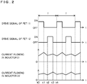
FIG. 2 is a timing chart illustrating the timing relationship between drive signals of FETs and current flowing through inductors in the voltage conversion device according toEmbodiment 1; -
FIG. 3 is a graph illustrating the relationship between a duty ratio and ripple current in the case where the leakage inductance is 2 µH; -
FIG. 4 is a graph illustrating the relationship between a duty ratio and ripple current in the case where the leakage inductance is 4 µH; -
FIG. 5 is an explanatory diagram illustrating magnetic fluxes interlinking with inductors through a core; -
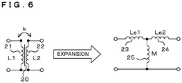
FIG. 6 is a circuit diagram illustrating an equivalent circuit of an inductor; -
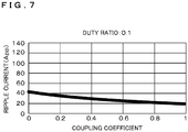
FIG. 7 is a graph illustrating the relationship between a coupling coefficient and ripple current in the case where the leakage inductance is 1 µH; -
FIG. 8 is a graph illustrating the relationship between a coupling coefficient and ripple current in the case where the leakage inductance is 1 µH; -
FIG. 9 is a graph illustrating the relationship between a coupling coefficient and ripple current in the case where the leakage inductance is 1 µH; -
FIG. 10 is a graph illustrating the relationship between a coupling coefficient and ripple current in the case where the leakage inductance is 1 µH; -
FIG. 11 is a graph illustrating the relationship between a coupling coefficient and ripple current in the case where the leakage inductance is 1 µH; -
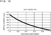
FIG. 12 is a graph illustrating the relationship between a coupling coefficient and ripple current in the case where the leakage inductance is 1 µH; -
FIG. 13 is a graph illustrating the relationship between a coupling coefficient and ripple current in the case where the leakage inductance is 1 µH; -
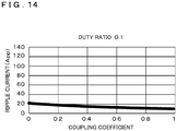
FIG. 14 is a graph illustrating the relationship between a coupling coefficient and ripple current in the case where the leakage inductance is 2 µH; -
FIG. 15 is a graph illustrating the relationship between a coupling coefficient and ripple current in the case where the leakage inductance is 2 µH; -
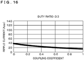
FIG. 16 is a graph illustrating the relationship between a coupling coefficient and ripple current in the case where the leakage inductance is 2 µH; -
FIG. 17 is a graph illustrating the relationship between a coupling coefficient and ripple current in the case where the leakage inductance is 2 µH; -
FIG. 18 is a graph illustrating the relationship between a coupling coefficient and ripple current in the case where the leakage inductance is 2 µH; -
FIG. 19 is a graph illustrating the relationship between a coupling coefficient and ripple current in the case where the leakage inductance is 2 µH; -
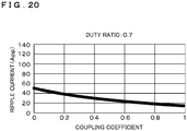
FIG. 20 is a graph illustrating the relationship between a coupling coefficient and ripple current in the case where the leakage inductance is 2 µH; -
FIG. 21 is a graph illustrating the relationship between a duty ratio and ripple current in the case where the leakage inductance is 2 µH; -
FIG. 22 is a graph illustrating the relationship between a duty ratio and ripple current before and after reduction in the leakage inductance; -
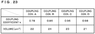
FIG. 23 is a table illustrating volume of a core measured for a coupling coil in the case where the leakage inductance is 0.9 µH; -
FIG. 24 is a graph illustrating waveforms of ripple current in the case where a reference coupling coil is used; -
FIG. 25 is a graph illustrating waveforms of ripple current in the case where a coupling coil A is used; -
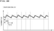
FIG. 26 is a graph illustrating waveforms of ripple current in the case where a coupling coil B is used; -
FIG. 27 is a graph illustrating waveforms of ripple current in the case where a coupling coil C is used; -
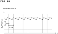
FIG. 28 is a graph illustrating a waveform of ripple current in the case where a coupling coil D is used; -
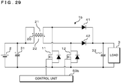
FIG. 29 is a block diagram illustrating a configuration example of a voltage conversion device according toEmbodiment 2; -
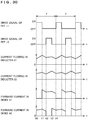
FIG. 30 is a timing chart illustrating the timing relationship between drive signals of FETs and current flowing through components in the voltage conversion device according toEmbodiment 2; -
FIG. 31 is a front diagram schematically illustrating an EE-type core of a voltage conversion device according to a variation example; -
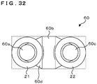
FIG. 32 is a plan diagram schematically illustrating an E-type core onto which inductors are fitted; and -
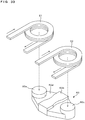
FIG. 33 is an explanatory diagram illustrating a method of assembling an EE-type core by fitting inductors onto the E-type core. - The technique disclosed in
Patent Document 1 describes that an inductor is short-circuited if the duty ratio for switching current flowing through the inductor exceeds 50%. It is thus assumed that an inductor with leakage inductance as close to 0 as possible, in other words, an inductor where k is substantially -1 is employed, greatly restricting the variable range of a duty ratio. - Moreover, the technique disclosed in
Patent Document 2 describes the range of the coupling coefficient k where the ripple current of the inductor is more reduced compared to the case where k is 0, if two inductors of constant self inductance are wound around a core of a certain size (or are so assumed from the description), which however is not directed to reduce the size of the core. Thus,Patent Document 2 neither discloses nor suggests any technique of reducing the size of a core in a range where the ripple current of the inductor is less increased compared to the case where the coupling coefficient k is 0. - The present invention has been made in view of the circumstances described above, and aims to provide a voltage conversion device with a reduced size of a core around which two inductors that magnetically cancel each other out are wound, and to provide a method of deciding leakage inductance capable of reducing the size of the core.
- According to the disclosure of the present application, the size of the core around which two inductors that magnetically cancel each other out are wound may be reduced.
- First, embodiments of the present invention will be listed in the following description. At least parts of the embodiments described below may arbitrarily be combined together.
- (1) A voltage conversion device according to one aspect of the present invention, comprises: a voltage conversion circuit including two inductors that are wound around a core and that magnetically cancel each other out, and switching elements that respectively switch current flowing through the two inductors; and a control unit that alternately turns on and off each of the switching elements, and the two inductors have a coupling coefficient in a range from - 0.99 to -0.78.
According to the present aspect, the control unit alternately turns on and off two switching elements in the voltage conversion circuit, and the switching elements respectively switch the current flowing through two inductors that are wound around a core and that magnetically cancel each other out, to convert voltage inputted to the voltage conversion circuit and output the converted voltage. The two inductors have the coupling coefficient k, which is closely related to the leakage inductance, within the range of -0.99 ≤ k ≤ - 0.78.
That is, such inductors may be applied that have k closer to - 1 than the conventional case (-0.4 < k ≤ -0.1 as described in Patent Document 2) in the range where ripple current of the inductor is less increased compared to the case where the coupling coefficient k between two inductors is 0, and that have leakage inductance smaller than the self inductance occurring when k is 0, as k becomes closer to -1. - (2) It is preferable that a magnitude of leakage inductance of the two inductors corresponds to a value less than one time and 0.45 times or more of a magnitude of self inductance that is required to reduce ripple current flowing through the two inductors at a predetermined reduction rate, in a case where the coupling coefficient of the two inductors is 0.
According to the present aspect, the magnitude of leakage inductance of two inductors is set as less than one time and equal to or more than 0.45 times of the magnitude of the self inductance which is required when the coupling coefficient is 0.
Thus, as the magnitude of leakage inductance is closer to a value 0.45 times the self inductance, the size of the core is reduced. - (3) It is preferable that a duty ratio at which the control unit turns on each of the switching elements is in a range from 0.1 to 0.7.
According to the present aspect, the current flowing through two inductors is switched at a duty ratio D in the range of 0.1 ≤ D ≤ 0.7.
This allows for switching at a higher duty ratio compared to the conventional case (D < 0.5 as described inPatent Document 1 or 0.05 ≤ D ≤ 0.40 as described in Patent Document 2), and thus higher output voltage may be obtained for the same input voltage. - (4) It is preferable that the voltage conversion device comprises N sets of the voltage conversion circuits (N is a natural number larger than 1), the N sets of the voltage conversion circuits are connected in parallel to one another, and the control unit turns on and off the switching elements of each of the voltage conversion circuits with phases each shifted by π/N.
According to the present aspect, the control unit alternately turns on and off two switching elements included in each of N voltage conversion circuits with a phase difference π, while turning on and off each one of the two switching elements with a phase shifted by π/N.
This may uniformly disperse switching losses to N voltage conversion circuits and may also reduce the ripple current contained in the output to 1/N. - (5) A method of deciding leakage inductance according to one aspect of the present invention is a method of deciding leakage inductance of two inductors in a voltage conversion device including switching elements that respectively switch current flowing through the two inductors that are wound around a core and magnetically cancel each other out, each of the switching elements being turned on or off by a control unit, comprising: preparing two first inductors with a coupling coefficient of 0, and two second inductors having leakage inductance of a same magnitude as self inductance of the first inductors and a coupling coefficient close to -1; connecting the two first inductors in place of the two inductors; obtaining a first change characteristic with respect to a duty ratio in a predetermined range where the control unit turns on each of the switching elements, for ripple current flowing through the first inductors; connecting the two second inductors in place of the two first inductors; obtaining a second change characteristic with respect to the duty ratio in the predetermined range, for ripple current flowing through the second inductors; calculating a reduction rate of ripple current based on a result obtained by comparing the obtained first and second change characteristics with each other; setting a reduction rate of the magnitude of leakage inductance of the second inductors to a reduction rate equal to or lower than the calculated reduction rate of ripple current; deciding a magnitude of leakage inductance of the two inductors so as to obtain the reduction rate; and setting a coupling coefficient of the two second inductors as a coupling coefficient of the two inductors.
According to the present aspect, the first change characteristic of ripple current with respect to a predetermined range of duty ratio that is obtained using two first inductors with the coupling coefficient k of 0 is successively compared with the second change characteristic of ripple current with respect to a predetermined range of duty ratio that is obtained using two second inductors having the same leakage inductance as the self inductance of the first inductors and having k close to -1 for a predetermined range of duty ratio, to decide leakage inductance of each of the two inductors based on the reduction rate of ripple current calculated from the result of comparison.
Thus, the reduction rate of ripple current that is reduced by k being close to -1 and the increase rate of ripple current that is increased by reducing leakage inductance are canceled out, which reduces the size of the core in accordance with the reduction in leakage inductance. - (6) It is preferable that the calculating of the reduction rate calculates a reduction rate of ripple current at one duty ratio where ripple current is reduced at a lowest rate in the second change characteristic with respect to the first change characteristic, the reduction rate of the magnitude of leakage inductance of the second inductors is set to a same reduction rate as the calculated reduction rate of ripple current, and the magnitude of leakage inductance of the two inductors is decided so as to obtain the reduction rate.
- According to the present aspect, the first and second change characteristics are successively compared with each other with respect to a predetermined range of duty ratio, the lowest reduction rate for the ripple current of the second change characteristic with respect to the ripple current of the first change characteristic is calculated, the magnitude of leakage inductance of the second inductors is reduced at a calculated reduction rate, and the leakage inductance with reduced magnitude is decided as leakage inductance for each of the two inductors.
- Since the reduction rate of ripple current guaranteed in the worst case for a predetermined range of duty ratio is thus calculated, in the case where the leakage inductance of each of two inductors is decided by reducing the magnitude of leakage inductance of the second inductors at the same reduction rate, the ripple current with respect to a predetermined range of duty ratio will not exceed the ripple current generated when the two first inductors are used.
- Specific examples of the voltage conversion device according to embodiments of the present invention will now be described below with reference to the drawings. It is to be noted that the present invention is defined by the appended claims rather than by the illustrated examples, while all changes that fall within metes and bounds of the claims, or equivalence of such metes and bounds thereof are therefore intended to be embraced by the claims. The technical features described in example embodiments may be combined with one another.
-
FIG. 1 is a block diagram illustrating a configuration example of a voltage conversion device according toEmbodiment 1. The voltage conversion device includes a voltage conversion circuit 1a that lowers the voltage supplied from anexternal power supply 2 and supplies the voltage to anexternal load 3, and acontrol unit 50a that controls conversion of voltage by the voltage conversion circuit 1a.Capacitors power supply 2 and theload 3. - The voltage conversion circuit 1a includes
inductors core 20 to cancel out magnetism caused by the current from thepower supply 2, and N-channel metal oxide semiconductor field effect transistors (MOSFET) (hereinafter referred to as FET) 11 and 12 that are switching elements to switch current flowing from thepower supply 2 to theinductors - The drain of each of the
FETs power supply 2, while the gate thereof is connected to thecontrol unit 50a. The source of each of theFETs inductors inductors load 3. Connection points between theinductors FETs FETs FETs control unit 50a. The negative side of thepower supply 2, the source of each of theFETs load 3 are connected to a common ground potential. - The
control unit 50a alternately turns on and off theFETs FETs control unit 50a applies drive signals having phases of on and off inverted from those of the drive signals of theFETs FETs inductors FETs - Ripple current flowing through the
inductors -
FIG. 2 is a timing chart illustrating the timing relationship between drive signals of theFETs inductors Embodiment 1. The four timing charts illustrated inFIG. 2 take the same time axis (t) as the horizontal axis, and indicate, from the top, drive signal of theFET 11, drive signal of theFET 12, current flowing in theinductor 21 and current flowing in theinductor 22. A variation component in the current flowing through theinductors control unit 50a turns on theFETs 11 and 12 (hereinafter simply referred to as duty ratio unless there is a risk of mix-up) is approximately 30%, for example. - Each signal and each current have cycles of T. The time at which the drive signals of the
FETs FETs FET 13 has inverted phase of on and off from the drive signal of theFET 11. That is, the drive signal of theFET 11 is off when the drive signal of theFET 13 is on, while the drive signal of theFET 11 is on except for a so-called dead time when the drive signal of theFET 13 is off. Likewise, the drive signal (not illustrated) of theFET 14 has inverted phase of on and off from the drive signal of theFET 12. - From the time t0 to t1, the
FET 11 is turned on, and current flows from thepower supply 2 through theinductor 21 to thecapacitor 32 and theload 3. During this period, energy is inputted from thepower supply 2 to theinductor 21, which increases current in theinductor 21. Though theother FET 12 is turned off, current is induced to theinductor 22 so as to cancel out the current flowing in theinductor 21, which increases current in theinductor 22 as time passes. This current flows back from thecapacitor 32 and theload 3 through theFET 14. - From the time t1 to t2, the
FET 11 is turned off, and the current flowing in theinductor 21 flows back through theFET 13. Moreover, the current flowing in theinductor 22 still flows back through theFET 14. During this period, no energy is inputted from thepower supply 2 to theinductor 21, which reduces current in both of theinductors - From the time t2 to t3, the
FET 12 is turned on, and current flows from thepower supply 2 through theinductor 22 to thecapacitor 32 and theload 3. The increased amount of current flowing through theinductor 22 during this period is equal to the increased amount of current in theinductor 21 during the period from time t0 to t1. Though theother FET 11 is turned off, current is induced to theinductor 21 so as to cancel out the current flowing in theinductor 22, which increases the current in theinductor 21 as time passes. This current flows back from thecapacitor 32 and theload 3 through theFET 13. - From the time t3 to t4, the
FET 12 is turned off, and the current flowing in theinductor 22 flows back through theFET 14. Moreover, the current flowing in theinductor 21 still flows back through theFET 13. During this period, no energy is inputted from thepower supply 2 to theinductors inductors - Here, assuming the case where no magnetic coupling occurs between the
inductors inductors inductor 21 during the period from t0 to t1 is represented by the following equation (1). The reduced amount of current flowing in theinductor 21 during the period from time t1 to t4 has the same absolute values as the equation (1) but different signs.
- where Vin: input voltage of voltage conversion circuit 1a (=voltage of power supply 2)
- Vout: output voltage of voltage conversion circuit 1a
- L1: self inductance of
inductor 21 - D: duty ratio at which
control unit 50a turns onFET 11 - T: cycle of drive signal of
FET 11 - Since the relationship between the input voltage Vin and the output voltage Vout in the voltage conversion circuit 1a is represented by the equation (2) below, the left side of the equation (2) is substituted for the right side of the equation (1) to obtain the equation (3) below which is deformed from the equation (1).


- The equation (3) represents that ripple current in the
inductor 21 is inversely proportional to the self inductance L1. According to the equation (3), ΔiL is 0 if the duty ratio is 0 or 1, whereas ΔiL is maximum if the duty ratio is 0.5. - On the other hand, if the coupling coefficient k between the
inductors inductor 21, corresponds to leakage inductance Le1 (seeFIG. 6 ), which will be described later. In the description below, the leakage inductance concerning theinductors inductor 21 generated in the case where the self inductance L1 in the equation (1) is substituted by the leakage inductance Le1 of the same magnitude is smaller than the case where k=0, since it is repeatedly increased or decreased more frequently than the case where k=0, as illustrated inFIG. 2 . - Particularly when k is as close to 1 as possible, at the duty ratio of 0.5, the current flowing in the
inductor 21 during a period where theFET 11 is turned on coincides with the current induced to theinductor 21 by theFET 12 during a period where theFET 11 is turned off, which reduces the ripple current of theinductor 21 to the minimum. It is apparent that the ripple current of theinductor 21 is 0 when the duty ratio is 0 or 1, as in the case where k=0. - In view of the discussion above, a simulation result for the relationship between the duty ratio and the ripple current will be described.
-
FIG. 3 is a graph illustrating the relationship between a duty ratio and ripple current in the case where the leakage inductance is 2 µH.FIG. 4 is a graph illustrating the relationship between a duty ratio and ripple current in the case where the leakage inductance is 4 µH. In each ofFIGS. 3 and4 , the horizontal axis represents the duty ratio whereas the vertical axis represents ripple current (App: Ampere peak-to-peak). - In
FIGS. 3 and4 , the solid lines and broken lines indicate the change characteristics of ripple current with respect to the duty ratio in the case where the coupling coefficients k are 0 and 0.99, respectively. While the leakage inductance may be referred to as "self inductance" if k=0, the term "leakage inductance" is used here. As discussed above, the ripple current generated if k=0 is maximum at the duty ratio of 0.5, forming an upward convex curve. On the other hand, the ripple current generated if k=0.99 is minimum of approximately 0 at the duty ratio of 0.5, forming curves where the ripple current is maximum at a duty ratio between 0 and 0.5 as well as between 0.5 and 1. - Comparing the cases indicated by solid lines in
FIGS. 3 and4 , if k=0, the ripple current is reduced to half over the entire range of duty ratio when the leakage inductance is doubled from 2µH to 4µH. Likewise, comparing the cases indicated by broken lines, if k=0.99, the ripple current is reduced to half over the entire range of duty ratio when the leakage inductance is doubled from 2µH to 4µH. That is, it can be said that the ripple current and the leakage inductance are inversely proportional to each other. - The relationship among the core 20, the
inductors -
FIG. 5 is an explanatory diagram illustrating magnetic fluxes interlinking with theinductor 21 and/or theinductor 22 through thecore 20.FIG. 6 is a circuit diagram illustrating an equivalent circuit of theinductors FIG. 5 is a so-called EI core, and a gap is formed at amiddle leg 20b between a part of the core 20 having an E shape and another part of the core 20 having an I shape. Thecore 20 is not limited to the EI core. Theinductors leg 20a on one side of thecore 20 and aleg 20c on the other side thereof, respectively. - Referring now to
FIG. 6 , the self inductance of theinductors inductors inductors inductors inductor 25 corresponding to mutual inductance M. Le1 and Le2 are represented by the following equations (4) and (5).

- The coupling coefficient k and the mutual inductance M are defined by the same sign, and whether k and M are positive or negative depends on the direction of magnetic coupling between the
inductors inductors - More specifically, in the case where current flows into one ends with dot signs of two inductors that are coupled to each other, if the magnetic fluxes are intensified (or weakened) with each other, the mutual inductance M is defined to have a positive (or negative) sign. Thus, it can be seen from the drawing that, in the case where the signs of the coupling coefficient k between the
inductors FIG. 1 as well as the mutual inductance M are defined as positive, the magnetic fluxes are weakened when current flows into one end of each of theinductors FETs inductors - To precisely illustrate
FIG. 1 by defining that the coupling coefficient k and mutual inductance M have a negative sign, dots are applied to one ends of theinductors FETs - Referring again to
FIG. 5 , in the case where voltage is applied from theFET 11 to one end of theinductor 21, excitation current im flows in theinductor 21, generating a main magnetic flux Φm in thecore 20 due to the excitation inductance corresponding to the mutual inductance M. The main magnetic flux Φm interlinks with theinductor 22 so that load current i2 flows by electromagnetic induction and load current i1 flows to theinductor 21 according to the load current i2. - Here, winding current (i1+im) by the
inductor 21 causes a leakage magnetic flux Φ1 not interlinking with theinductor 22, and winding current (i2) by theinductor 22 causes a leakage magnetic flux Φ2 not interlinking with theinductor 21. The leakage magnetic fluxes Φ1 and Φ2 pass through theleg 20b at the middle of thecore 20. Using the leakage inductance Le1 and Le2 as described above, the leakage magnetic fluxes Φ1 and Φ2 are represented by the following equations (6) and (7).

- While the main magnetic flux Φm is not increased by the load current i1 and i2, leakage magnetic fluxes Φ1 and Φ2 are increased respectively in proportion to the load current i1 and i2. Thus, in the case where the load current i1 and i2 are constant, the equations (6) and (7) indicate that the magnetic flux (magnetic flux density) Φ in the
core 20 is proportional to the leakage inductance Le1 and Le2. It is assumed in the description below that comparison is made while the load current i1 and i2 are set to be constant. Since the magnetic flux Φ is represented by the product of magnetic density B in thecore 20 and an effective sectional area Ae of the core 20, if the magnetic density B in thecore 20 is constant, the effective sectional area Ae and the leakage inductance Le1 and Le2 may bear a proportional relationship. - In general, the magnetic flux density in the core cannot exceed the maximum magnetic flux density Bmax. In view of this, when, for example, the size of the core is reduced without changing the shape thereof, the leakage inductance may be lowered by a rate at which the effective sectional area is reduced, based on the proportional relationship described above, in order to reduce the effective sectional area of the core without changing the magnetic flux density of the core. There is, however, a dilemma where ripple current is increased by lowering the leakage inductance in order to reduce the size of the core, since the ripple current and leakage inductance are inversely proportional to each other as described above.
- To find ways to reduce the size of the core in a range where the ripple current of the inductor is less increased compared to the case where the coupling coefficient k is 0, graphs are plotted that indicate the changes in ripple current in the case where two inductors with constant leakage inductance and varied coupling coefficients are used.
-
FIGS. 7 to 13 are graphs illustrating the relationship between coupling coefficients and ripple current in the case where the leakage inductance is 1 µH.FIGS. 14 to 20 are graphs illustrating the relationship between coupling coefficients and ripple current in the case where the leakage inductance is 2 µH. In each of the drawings, the horizontal axis represents coupling coefficients whereas the vertical axis represents ripple current (App).FIGS. 7 ,8 ,9 ,10 ,11 ,12 and13 as well asFIGS. 14 ,15 ,16 ,17 ,18 ,19 and20 illustrate changes in ripple current depending on the coupling coefficients for the cases where the duty ratios are 0.1, 0.2, 0.3, 0.4, 0.5, 0.6 and 0.7, respectively. Here, the voltage of thepower supply 2 is 48V, whereas the cycle T is 10µs (frequency of 100 kHz). - It can be seen from any one of
FIGS. 7 to 20 that ripple current is more reduced as the coupling coefficient is larger. Focusing on this point, one graph is plotted based on the graphs illustrated inFIGS. 14 to 20 in order to evaluate how the ripple current changes when the duty ratio is changed in the case where the leakage inductance is 2µH. -
FIG. 21 is a graph illustrating the relationship between a duty ratio and ripple current in the case where the leakage inductance is 2 µH. In the drawing, the horizontal axis represents a duty ratio whereas the vertical axis represents ripple current (App). The solid line, broken line and dashed-dotted line indicate the change characteristics of the ripple current with respect to the duty ratio when the coupling coefficients k are 0.0, 0.9 and 0.99, respectively. As described above, it is apparent that the ripple current is more reduced as the coupling coefficient k is larger, and thus no graph is plotted for the cases where the coupling coefficient k is larger than 0.0 and smaller than 0.9. - When seen from another perspective, the solid line in
FIG. 21 indicates the first change characteristic of the ripple current for the duty ratio in the range from 0 to 1 that is obtained using two first inductors with the leakage inductance (corresponding to self inductance in practice) of 2µH and the coupling coefficient k of 0. Moreover, the broken line or dashed-dotted line inFIG. 21 indicate the second change characteristic of the ripple current for the duty ratio in the range from 0 to 1 that is obtained using two second inductors with the leakage inductance of the same magnitude as the self inductance of the first inductor and k close to -1. These change characteristics are successively compared with one another across a certain range of duty ratio, and the lowest reduction rate for the ripple current of the second change characteristic to the ripple current of the first change characteristic may be calculated based on the values read fromFIG. 21 . - It has been found here, as described above, that the ripple current is inversely proportional to the leakage inductance and that the effective sectional area of the core is reduced by the amount the leakage inductance is reduced while the magnetic density in the core is made constant. Accordingly, the rate at which the ripple current is increased by reducing the leakage inductance of the second inductance by the amount corresponding to the reduction rate calculated by reading values from
FIG. 21 and the rate at which the ripple current is reduced by changing k from 0 to 0.99 may be canceled out. It is thus possible to reduce the size of the core without changing the magnetic flux density within the core in a range where the ripple current of the inductor is less increased compared to the case where the coupling coefficient k is 0. - More specifically, if, for example, the duty ratio is changed from 0.1 to 0.7 in
FIG. 21 , the rate of reducing the ripple current when the coupling coefficient k is changed from 0 to 0.99 is the lowest when the duty ratio is 0.1, the reduction rate here being 0.55. In other words, the ripple current is reduced to only 0.45 times by changing k from 0 to 0.99 with the duty ratio of 0.1, whereas the ripple current is more reduced to less than 0.45 times with the other duty ratios. Thus, by reducing the leakage inductance to 0.9µH which is 0.45 times of 2µH and by setting the coupling coefficient k to 0.99, it is possible to less increase the ripple current for the duty ratio in the range from 0.1 to 0.7, compared to the case where k is 0. By reducing the leakage inductance to 0.45 times (reduction rate of 0.55), the size (effective sectional area) of the core may also be 0.45 times without changing the magnetic flux density in the core. - Effects on ripple current will now be described that is caused by the reduction in the leakage inductance and the change of k from 0 to 0.99.
-
FIG. 22 is a graph illustrating the relationship between a duty ratio and ripple current before and after the leakage inductance is reduced. In the drawing, the horizontal axis represents a duty ratio whereas the vertical axis represents ripple current (App). The solid line in the drawing indicates the change characteristic of ripple current with respect to the duty ratio at a time when the leakage inductance (leakage L) is 2µH and k=0. This solid line is exactly the same as that inFIG. 21 . Furthermore, the broken line indicates the change characteristic of ripple current with respect to the duty ratio at a time when the leakage inductance is 0.9µH and k=0.99. - The ripple current indicated by the broken line shows a curve where it is minimized to approximately 0 when the duty ratio is 0.5, and is maximized when the duty ratio is between 0 and 0.5 as well as between 0.5 and 1, as in the cases shown in
FIGS. 3 and4 . Referring toFIG. 22 , even in the case where the leakage inductance is reduced from 2µH to 0.9µH and k is changed from 0 to 0.99, the increase in ripple current is suppressed across the range of a duty ratio of at least from 0.1 to 0.7. - A confirmation result of the effect of reducing the size of the core will now be described.
-
FIG. 23 is a table illustrating the volume of the core actually measured for the coupling coil in the case where the leakage inductance is 0.9µH. Here, four types of coupling coils A, B, C and D are experimentally produced, with the leakage inductance of 0.9µH obtained by coupling two inductors through a core, to have coupling coefficients of 0.78, 0.86, 0.96 and 0.98, respectively, and the effect of reduction in the size of the core is confirmed by actually measuring the volume of the core. - As a result of the measurement, the values of the volume of the cores for the coupling coils A, B, C and D are 22cm3, 24cm3, 23cm3 and 21cm3, respectively. Meanwhile, as for a reference coupling coil with the leakage inductance of 2.0µH and k=0, which is used for reference in comparison, the volume of the core is 38cm3. It can be said from these results that the effect of sufficiently reducing the size of the core may be obtained over a wide range where k is from 0.78 to 0.98.
- Finally, ripple current generated in the case where the coupling coils A, B, C and D are used will be described.
-
FIG. 24 is a graph illustrating waveforms of ripple current in the case where a reference coupling coil is used.FIGS. 25 ,26 ,27 and28 are graphs illustrating waveforms of ripple current in the cases where coupling coils A, B, C and D are used, respectively. In each of the drawings, the horizontal axis represents time (t) whereas the vertical axis represents current (A) in theinductor FIGS. 24 to 28 . As for the measurement conditions, the input voltage is 24V, the output current is approximately 70A, the frequency is 80kH and the duty ratio is 0.6. - Since the magnitude of current amplitude matters here,
FIGS. 24 to 28 illustrate waveforms of ripple current in two inductors included in the coupling coils without distinguishing one from another. It can be found from these drawings that the phases of the waveforms of two kinds of ripple current are shifted from each other by π. It can further be seen that the ripple current illustrated inFIGS. 25 to 28 is suppressed to be equal to or lower than the ripple current shown inFIG. 24 . - While the reduction rate of ripple current generated when k is changed from 0 to 0.99 (-0.99 in practice) is calculated using
FIG. 21 , it is not always necessary to increase k up to 0.99. It is apparent from the description above that the reduction rate of ripple current is larger as k is closer to 1 (-1 in practice), and the size of the core 20 may be reduced at a larger rate as the ripple current is reduced at a larger rate. - As described above, according to
Embodiment 1, thecontrol unit 50a alternately turns on and off theFETs FETs inductors core 20 and that magnetically cancel each other out, and thus the voltage inputted to the voltage conversion circuit 1a is converted and outputted. For theinductors - That is, in a range where the ripple current in the
inductors inductors - Accordingly, the size of the
core 20 around which theinductors - Moreover, according to
Embodiment 1, the current flowing through theinductors - Accordingly, the duty ratio higher than the conventional case (D < 0.5 as described in
Patent Document 1, or 0.05 ≤ D ≤ 0.40 as described in Patent Document 2) may be employed, which may obtain higher output voltage for the same input voltage. - Furthermore, according to
Embodiment 1, the first change characteristic of the ripple current for the duty ratio in the range from 0 to 1 that is obtained using two first inductors with the coupling coefficient k of 0 is successively compared with the second change characteristic of the ripple current for the duty ratio in the range from 0 to 1 that is obtained using two second inductors with the leakage inductance of the same magnitude as the self inductance of the first inductors and k close to -1, across the duty ratio in the range from 0.1 to 0.7, and the leakage inductance Le1 and Le2 are decided for theinductors - Thus, the reduction rate of ripple current that is reduced by k being closer to -1 and the increase rate of ripple current that is increased by reducing leakage inductance Le1 and Le2 are canceled out, so that the size of the core 20 may be reduced in accordance with the reduction in leakage inductance Le1 and Le2.
- Furthermore, according to
Embodiment 1, the first change characteristic is successively compared with the second change characteristic across the duty ratio in the range from 0.1 to 0.7, the lowest reduction rate (=0.45) is calculated for the ripple current in the second change characteristic with respect to the ripple current in the first change characteristic, the leakage inductance for the second inductor is reduced at the calculated reduction rate, and the reduced leakage inductance is decided as the leakage inductance Le1 and Le2 for theinductors - As such, the reduction rate of ripple current to be guaranteed in the worst case for the duty ratio in the range from 0.1 to 0.7 is calculated, which allows the ripple current for the duty ratio in the range from 0.1 to 0.7 to be equal to or less than the ripple current generated when two first inductors are used, in the case where the leakage inductance of the second inductor is reduced at the same reduction rate and the leakage inductance for the
respective inductors - While
Embodiment 1 described the example where the voltage of thepower supply 2 is lowered in the voltage conversion circuit 1a,Embodiment 2 describes an example where the voltage of thepower supply 2 is increased in a voltage conversion circuit. -
FIG. 29 is a block diagram illustrating a configuration example of a voltage conversion device according toEmbodiment 2. The voltage conversion device includes avoltage conversion circuit 1b in which the voltage supplied from anexternal power supply 2 is raised and supplied to anexternal load 3, and acontrol unit 50b that controls conversion of voltage by thevoltage conversion circuit 1b.Capacitors power supply 2 and theload 3. - The
voltage conversion circuit 1b includesinductors core 20 and that cancel out magnetism caused by the current from thepower supply 2, and also includesFETs power supply 2 through therespective inductors inductors power supply 2. The other end of theinductor 21 is connected to the drain of theFET 11 and to the anode of adiode 41. The other end of theinductor 22 is connected to the drain of theFET 12 and the anode of adiode 42. The gate of each of theFETs control unit 50b. The cathode of each of thediodes load 3. The negative side of thepower supply 2, the source of each of theFETs load 3 are connected to a common ground potential. - The
control unit 50b alternately turns on and off theFETs FETs Embodiment 1 will be denoted by the same reference codes and will not be described here. - Ripple current flowing through the
inductors -
FIG. 30 is a timing chart illustrating the timing relationship between drive signals of theFETs Embodiment 2 and current flowing through each component. The six timing charts illustrated inFIG. 6 take the same time axis (t) as the horizontal axis, and indicate, from the top, the drive signal of theFET 11, the drive signal of theFET 12, the current flowing through theinductor 21, the current flowing through theinductor 22, forward current in thediode 41 and forward current in thediode 42. A variation component of the current flowing through theinductors control unit 50b turns on theFETs 11 and 12 (hereinafter simply referred to as duty ratio unless there is a risk of mix-up) is approximately 30%, for example. - Each signal and each current have the cycle of T. The time at which the drive signals of the
FETs FETs - From the time t0 to t1, the
FET 11 is turned on, and current flows from thepower supply 2 to theinductor 21. During this period, energy is inputted from thepower supply 2 to theinductor 21, which increases current in theinductor 21. Though theother FET 12 is off, current is induced to theinductor 22 so as to cancel out the current flowing in theinductor 21, which increases the current in theinductor 22 as time passes. This current flows to thecapacitor 32 andload 3 through thediode 42. - From the time t1 to t2, the
FET 11 is turned off, and the current flowing in theinductor 21 flows back through thediode 41 as well as thecapacitor 32 and theload 3. Moreover, the current flowing in theinductor 22 still flows to thecapacitor 32 and theload 3 through thediode 42. During this period, no energy is inputted from thepower supply 2 to theinductors inductors - From the time t2 to t3, the
FET 12 is turned on, and current flows from thepower supply 2 to theinductor 22. The increased amount of current flowing through theinductor 22 during this period is equal to the increased amount of current in theinductor 21 flowing during the period from time t0 to t1. Though theother FET 11 is off, current is induced to theinductor 21 so as to cancel out the current flowing in theinductor 22, which increases the current in theinductor 21 as time passes. This current flows to thecapacitor 32 and theload 3 through thediode 41. - From the time t3 to t4, the
FET 12 is turned off, and the current flowing in theinductor 22 flows back through thediode 42 as well as thecapacitor 32 and theload 3. Moreover, the current flowing in theinductor 21 still flows to thecapacitor 32 and theload 3 through thediode 41. During this period, no energy is inputted from thepower supply 2 to theinductors inductors - Here, assuming the case where no magnetic coupling occurs between the
inductors inductors inductor 21 during the period from t0 to t1 is represented by the following equation (8). The reduced amount of current flowing in theinductor 21 during the period from time t1 to t4 has the same absolute values as the equation (8) but different signs.
- where Vin: input voltage of
voltage conversion circuit 1b (=voltage of power supply 2) - L1: self inductance of
inductor 21 - D: duty ratio at which
control unit 50b turns onFET 11 - T: cycle of drive signal of
FET 11 - The equation (8) represents that ripple current of the
inductor 21 is inversely proportional to the self inductance L1 and is proportional to the duty ratio. - Meanwhile, if the coupling coefficient k between the
inductors inductor 21 that substitutes for the self inductance L1 in the equation (8) and that serves as a choke coil is the leakage inductance Le1 (seeFIG. 6 ). In the description below, the leakage inductance concerning theinductors inductor 21 generated in the case where the self inductance L1 in the equation (8) is substituted by the leakage inductance Le1 of the same magnitude is smaller than that in the case where k=0, since it is repeatedly increased or decreased more frequently than the case where k=0 as illustrated inFIG. 30 . - Particularly when k is as close to 1 as possible, at the duty ratio of 0.5, the current flowing in the
inductor 21 during a period where theFET 11 is turned on coincides with the current induced to theinductor 21 by theFET 12 during a period where theFET 11 is turned off, which reduces the ripple current of theinductor 21 to the minimum. - In
Embodiment 2, it is apparent that the ripple current and leakage inductance are inversely proportional to each other, as inEmbodiment 1. It can also be seen, as inEmbodiment 1, that the effective sectional area of the core and leakage inductance are proportional to each other in the case where the magnetic flux density in the core is constant. Though not illustrated, similarly toEmbodiment 1, the ripple current is more reduced as the coupling coefficient k is made closer to 1 with constant leakage inductance. - Thus, as in
FIG. 21 ofEmbodiment 1, graphs are plotted that indicate the first and second change characteristics of ripple current with respect to the duty ratio in the range from 0 to 1 in the case where the coupling coefficients k are 0 and 0.99 with constant leakage inductance. The plotted graphs of the first and second change characteristics are successively compared with each other across the duty ratio in the range from 0.1 to 0.7, and the leakage inductance Le1 and Le2 for therespective inductors - Thus, the reduction rate of ripple current that is reduced by k being closer to -1 and the increase rate of ripple current that is increased by reducing leakage inductance Le1 and Le2 are canceled out, so that the size of the core 20 may be reduced in accordance with the reduction in leakage inductance Le1 and Le2.
- While only one voltage conversion circuit 1a (or 1b) is included in Embodiment 1 (or 2), the number of voltage conversion circuits 1a (or 1b) is not limited to one but may be N (N is a natural number larger than 1) that are connected in parallel.
- In the case of including N voltage conversion circuits 1a (or 1b), the
control unit 50a (or 50b) alternately turns on and off theFETs FETs - That is, all the FETs 11 and 12 included in the N voltage conversion circuits 1a (or 1b) are turned on and off with phases each shifted by 2π/N.
- This may uniformly disperse switching losses to N voltage conversion circuits 1a (or 1b) and may also reduce the ripple current contained in the output to 1/N.
- While
Embodiments type core 20, an EE-type core is used in Variation Example.FIG. 31 is a front diagram schematically illustrating an EE-type core 600 of a voltage conversion device according to Variation Example.FIG. 32 is a plan diagram schematically illustrating anE-type core 60 onto which theinductors FIG. 33 is an explanatory diagram illustrating a method of assembling the EE-type core 600 by fitting theinductors E-type core 60. - The EE-
type core 600 includes twoE-type cores 60 each having a diamond-shapedplanar part 60d as well asouter legs middle leg 60b protruding from one surface of theplanar part 60d in the vertical direction. Theouter legs E-type cores 60 are butted with theouter legs E-type cores 60, respectively. The length of themiddle leg 60b of eachE-type core 60 is shorter than the length of theouter legs type core 600, themiddle legs E-type cores gap 601. - The
outer legs E-type core 60 has a cylindrical shape, and has a diameter in the direction crossing the axial direction being a little smaller than the inner diameter of the winding diameter of theinductors middle leg 60b has a wide I shape in plan view, and has a narrowed portion at a part opposed to the outer circumferential sides of theinductors - Referring to
FIG. 33 , theinductors outer legs E-type cores 60 along the direction of the winding axis indicated by the broken arrows. Thereafter, theother E-type core 60 inverted in the vertical direction is placed over the oneE-type core 60. Here, as described above, theouter legs 60a are butted with each other and also theouter legs 60c are butted with each other. In the case where the EE-type core 600 assembled as described above is applied to the voltage conversion device, winding current flows in the direction indicated by the solid arrows, for example, in theinductors - According to the present variation example, as described above, the EE-
type core 600 may be produced from two separateE-type cores 60, eliminating the need for more than one metal mold. Moreover, theouter legs middle leg 60b is provided with a narrowed portion, which can reduce unwanted gaps between the inner circumferential sides of theinductors outer legs inductors middle leg 60b. Thus, the void ratio of the entire EE-type core 600 onto which theinductors type core 600 may be reduced while maintaining the effective sectional area constant. It is noted that the void ratio here represents the rate of a gap occupying the volume of a rectangular parallelepiped, which is decided by the product of the height of the EE-type core 600 illustrated inFIG. 31 , and the width and depth of the EE-type core 600 including theinductors FIG. 32 . -
- 1a, 1b voltage conversion circuit
- 11, 12, 13, 14 FET
- 20 core
- 20a, 20b, 20c leg
- 21, 22 inductor
- 31, 32 capacitor
- 41, 42 diode
- 50a, 50b control unit
- 600 EE-type core
- 601 gap
- 60 E-type core
- 60a, 60c outer leg
- 60b middle leg
- 60d planar part
- 2 power supply
- 3 load
Claims (6)
- A voltage conversion device, comprising:a voltage conversion circuit including two inductors that are wound around a core and that magnetically cancel each other out, and switching elements that respectively switch current flowing through the two inductors; anda control unit that alternately turns on and off each of the switching elements,wherein the two inductors have a coupling coefficient in a range from -0.99 to -0.78.
- The voltage conversion device according to claim 1, wherein a magnitude of leakage inductance of the two inductors corresponds to a value less than one time and 0.45 times or more of a magnitude of self inductance that is required to reduce ripple current flowing through the two inductors at a predetermined reduction rate, in a case where the coupling coefficient of the two inductors is 0.
- The voltage conversion device according to claim 1 or 2, wherein a duty ratio at which the control unit turns on each of the switching elements is in a range from 0.1 to 0.7.
- The voltage conversion device according to any one of claims 1 to 3, comprising N sets of the voltage conversion circuits (N is a natural number larger than 1),
wherein
the N sets of the voltage conversion circuits are connected in parallel to one another, and
the control unit turns on and off the switching elements of each of the voltage conversion circuits with phases each shifted by π/N. - A method of deciding leakage inductance of two inductors in a voltage conversion device including switching elements that respectively switch current flowing through the two inductors that are wound around a core and magnetically cancel each other out, each of the switching elements being turned on or off by a control unit, comprising:preparing two first inductors with a coupling coefficient of 0, and two second inductors having leakage inductance of a same magnitude as self inductance of the first inductors and a coupling coefficient close to -1;connecting the two first inductors in place of the two inductors;obtaining a first change characteristic with respect to a duty ratio in a predetermined range where the control unit turns on each of the switching elements, for ripple current flowing through the first inductors;connecting the two second inductors in place of the two first inductors;obtaining a second change characteristic with respect to the duty ratio in the predetermined range, for ripple current flowing through the second inductors;calculating a reduction rate of ripple current based on a result obtained by comparing the obtained first and second change characteristics with each other;setting a reduction rate of the magnitude of leakage inductance of the second inductors to a reduction rate equal to or lower than the calculated reduction rate of ripple current;deciding a magnitude of leakage inductance of the two inductors so as to obtain the reduction rate; andsetting a coupling coefficient of the two second inductors as a coupling coefficient of the two inductors.
- The method of deciding leakage inductance according to claim 5, wherein
the calculating of the reduction rate calculates a reduction rate of ripple current at one duty ratio where ripple current is reduced at a lowest rate in the second change characteristic with respect to the first change characteristic,
the reduction rate of the magnitude of leakage inductance of the second inductors is set to a same reduction rate as the calculated reduction rate of ripple current, and
the magnitude of leakage inductance of the two inductors is decided so as to obtain the reduction rate.
Applications Claiming Priority (2)
| Application Number | Priority Date | Filing Date | Title |
|---|---|---|---|
| JP2016116530A JP6149977B1 (en) | 2016-06-10 | 2016-06-10 | Voltage converter and leakage inductance determination method |
| PCT/JP2017/019827 WO2017212954A1 (en) | 2016-06-10 | 2017-05-29 | Voltage conversion device and leakage inductance determination method |
Publications (2)
| Publication Number | Publication Date |
|---|---|
| EP3471250A1 true EP3471250A1 (en) | 2019-04-17 |
| EP3471250A4 EP3471250A4 (en) | 2020-01-22 |
Family
ID=59081958
Family Applications (1)
| Application Number | Title | Priority Date | Filing Date |
|---|---|---|---|
| EP17810133.3A Withdrawn EP3471250A4 (en) | 2016-06-10 | 2017-05-29 | VOLTAGE CONVERSION DEVICE AND LEAKAGE INDUCTANCE DETERMINATION METHOD |
Country Status (5)
| Country | Link |
|---|---|
| US (1) | US10483851B2 (en) |
| EP (1) | EP3471250A4 (en) |
| JP (1) | JP6149977B1 (en) |
| CN (1) | CN109314462B (en) |
| WO (1) | WO2017212954A1 (en) |
Families Citing this family (7)
| Publication number | Priority date | Publication date | Assignee | Title |
|---|---|---|---|---|
| US11695337B2 (en) | 2018-12-21 | 2023-07-04 | Cirrus Logic, Inc. | Current control for a boost converter with dual anti-wound inductor |
| CN113472176B (en) | 2020-03-30 | 2023-03-14 | 台达电子工业股份有限公司 | power conversion system |
| JP7279694B2 (en) | 2020-08-25 | 2023-05-23 | トヨタ自動車株式会社 | Control device |
| JP7230890B2 (en) * | 2020-08-25 | 2023-03-01 | トヨタ自動車株式会社 | power converter |
| CN113315376A (en) * | 2021-06-21 | 2021-08-27 | 哈尔滨工业大学 | Variable-weight DCDC converter based on current ripple optimization |
| CN118251829A (en) * | 2021-11-12 | 2024-06-25 | 思睿逻辑国际半导体有限公司 | Current Control of Boost Converter with Dual Back-Wound Inductors |
| JP7589678B2 (en) | 2021-12-23 | 2024-11-26 | トヨタ自動車株式会社 | Power System |
Family Cites Families (11)
| Publication number | Priority date | Publication date | Assignee | Title |
|---|---|---|---|---|
| US6362986B1 (en) * | 2001-03-22 | 2002-03-26 | Volterra, Inc. | Voltage converter with coupled inductive windings, and associated methods |
| JP3751306B2 (en) | 2004-02-06 | 2006-03-01 | 本田技研工業株式会社 | DC / DC converter and program |
| US7199695B1 (en) * | 2005-10-25 | 2007-04-03 | Virginia Tech Intellectual Properties, Inc. | Multiphase voltage regulator having coupled inductors with reduced winding resistance |
| EP1835604A1 (en) * | 2006-03-16 | 2007-09-19 | STMicroelectronics S.r.l. | Magnetic core for a coupled multi coil filter inductor |
| HRP20140049T1 (en) | 2007-01-05 | 2014-02-28 | University Of Zürich | Anti-beta-amyloid antibody and uses thereof |
| JP5144284B2 (en) * | 2008-01-16 | 2013-02-13 | 本田技研工業株式会社 | Power conversion circuit |
| JP5049245B2 (en) * | 2008-10-21 | 2012-10-17 | 株式会社豊田中央研究所 | Multi-phase converter for on-vehicle use |
| JP5862918B2 (en) * | 2010-06-23 | 2016-02-16 | トヨタ自動車株式会社 | Multiphase converter and design method of multiphase converter |
| US20120319478A1 (en) * | 2011-06-20 | 2012-12-20 | Volterra Semiconductor Corporation | Dc to dc converter with ripple cancellation |
| JP2015056940A (en) * | 2013-09-11 | 2015-03-23 | 株式会社デンソー | Filter circuit for multiphase power converter and multiphase power converter |
| JP6152828B2 (en) * | 2014-06-06 | 2017-06-28 | 株式会社村田製作所 | Multi-phase DC / DC converter |
-
2016
- 2016-06-10 JP JP2016116530A patent/JP6149977B1/en active Active
-
2017
- 2017-05-29 EP EP17810133.3A patent/EP3471250A4/en not_active Withdrawn
- 2017-05-29 CN CN201780035996.1A patent/CN109314462B/en active Active
- 2017-05-29 US US16/308,736 patent/US10483851B2/en active Active
- 2017-05-29 WO PCT/JP2017/019827 patent/WO2017212954A1/en not_active Ceased
Also Published As
| Publication number | Publication date |
|---|---|
| US10483851B2 (en) | 2019-11-19 |
| US20190149049A1 (en) | 2019-05-16 |
| EP3471250A4 (en) | 2020-01-22 |
| WO2017212954A1 (en) | 2017-12-14 |
| CN109314462A (en) | 2019-02-05 |
| CN109314462B (en) | 2021-01-05 |
| JP6149977B1 (en) | 2017-06-21 |
| JP2017221088A (en) | 2017-12-14 |
Similar Documents
| Publication | Publication Date | Title |
|---|---|---|
| US10483851B2 (en) | Voltage conversion device and method of deciding leakage inductance | |
| US10211745B2 (en) | Resonant LLC converter with a multi-leg transformer with gapped center leg | |
| US10742123B1 (en) | Low common mode noise transformers and switch-mode DC-DC power converters | |
| US6549436B1 (en) | Integrated magnetic converter circuit and method with improved filtering | |
| EP1082735B1 (en) | Variable inductor | |
| US9019061B2 (en) | Magnetic device formed with U-shaped core pieces and power converter employing the same | |
| US7167384B2 (en) | Switching power circuit | |
| EP2526615B1 (en) | Power conversion with zero voltage switching | |
| JP6745911B2 (en) | Power converter | |
| US7183754B2 (en) | DC/DC converter | |
| US10886859B2 (en) | Alternating-current power supply device with windings wound in different directions | |
| JP4175367B2 (en) | Switching power supply | |
| US6252383B1 (en) | Buck and boost power converters with non-pulsating input and output terminal currents | |
| JP2005278380A (en) | Switching power supply unit | |
| EP3451518A1 (en) | Llc resonant converter | |
| US11245342B2 (en) | AC power supply device | |
| JP2005051995A (en) | DC-DC converter | |
| US6198644B1 (en) | Rectifying/smoothing circuit and double-ended converter | |
| JP2018014841A (en) | Voltage converter, step-down control method of power conversion circuit, step-up control method of power conversion circuit and computer program | |
| US20060208712A1 (en) | DC/DC converter | |
| JPH0864439A (en) | Converter transformer | |
| JP2003092876A (en) | Switching power supply | |
| JP2003092877A (en) | Switching power supply | |
| JP5360427B2 (en) | Power supply | |
| JP2008054378A (en) | DC-DC converter |
Legal Events
| Date | Code | Title | Description |
|---|---|---|---|
| STAA | Information on the status of an ep patent application or granted ep patent |
Free format text: STATUS: THE INTERNATIONAL PUBLICATION HAS BEEN MADE |
|
| PUAI | Public reference made under article 153(3) epc to a published international application that has entered the european phase |
Free format text: ORIGINAL CODE: 0009012 |
|
| STAA | Information on the status of an ep patent application or granted ep patent |
Free format text: STATUS: REQUEST FOR EXAMINATION WAS MADE |
|
| 17P | Request for examination filed |
Effective date: 20181210 |
|
| AK | Designated contracting states |
Kind code of ref document: A1 Designated state(s): AL AT BE BG CH CY CZ DE DK EE ES FI FR GB GR HR HU IE IS IT LI LT LU LV MC MK MT NL NO PL PT RO RS SE SI SK SM TR |
|
| AX | Request for extension of the european patent |
Extension state: BA ME |
|
| DAV | Request for validation of the european patent (deleted) | ||
| DAX | Request for extension of the european patent (deleted) | ||
| A4 | Supplementary search report drawn up and despatched |
Effective date: 20200103 |
|
| RIC1 | Information provided on ipc code assigned before grant |
Ipc: H02M 3/155 20060101AFI20191218BHEP Ipc: H02M 1/14 20060101ALN20191218BHEP Ipc: H02M 3/158 20060101ALI20191218BHEP |
|
| STAA | Information on the status of an ep patent application or granted ep patent |
Free format text: STATUS: EXAMINATION IS IN PROGRESS |
|
| 17Q | First examination report despatched |
Effective date: 20210728 |
|
| RIC1 | Information provided on ipc code assigned before grant |
Ipc: H02M 3/155 20060101AFI20251219BHEP Ipc: H02M 3/158 20060101ALI20251219BHEP Ipc: H02M 1/14 20060101ALN20251219BHEP |
|
| GRAP | Despatch of communication of intention to grant a patent |
Free format text: ORIGINAL CODE: EPIDOSNIGR1 |
|
| STAA | Information on the status of an ep patent application or granted ep patent |
Free format text: STATUS: GRANT OF PATENT IS INTENDED |
|
| RIC1 | Information provided on ipc code assigned before grant |
Ipc: H02M 3/155 20060101AFI20260123BHEP Ipc: H02M 3/158 20060101ALI20260123BHEP Ipc: H02M 1/14 20060101ALN20260123BHEP |
|
| INTG | Intention to grant announced |
Effective date: 20260218 |
|
| STAA | Information on the status of an ep patent application or granted ep patent |
Free format text: STATUS: THE APPLICATION HAS BEEN WITHDRAWN |
|
| 18W | Application withdrawn |
Effective date: 20260526 |