EP3471216A1 - Electrical connector - Google Patents
Electrical connector Download PDFInfo
- Publication number
- EP3471216A1 EP3471216A1 EP18199380.9A EP18199380A EP3471216A1 EP 3471216 A1 EP3471216 A1 EP 3471216A1 EP 18199380 A EP18199380 A EP 18199380A EP 3471216 A1 EP3471216 A1 EP 3471216A1
- Authority
- EP
- European Patent Office
- Prior art keywords
- contacts
- housing
- contact
- connector
- electrical connector
- Prior art date
- Legal status (The legal status is an assumption and is not a legal conclusion. Google has not performed a legal analysis and makes no representation as to the accuracy of the status listed.)
- Granted
Links
Images




Classifications
-
- H—ELECTRICITY
- H01—ELECTRIC ELEMENTS
- H01R—ELECTRICALLY-CONDUCTIVE CONNECTIONS; STRUCTURAL ASSOCIATIONS OF A PLURALITY OF MUTUALLY-INSULATED ELECTRICAL CONNECTING ELEMENTS; COUPLING DEVICES; CURRENT COLLECTORS
- H01R43/00—Apparatus or processes specially adapted for manufacturing, assembling, maintaining, or repairing of line connectors or current collectors or for joining electric conductors
- H01R43/20—Apparatus or processes specially adapted for manufacturing, assembling, maintaining, or repairing of line connectors or current collectors or for joining electric conductors for assembling or disassembling contact members with insulating base, case or sleeve
- H01R43/24—Assembling by moulding on contact members
-
- H—ELECTRICITY
- H01—ELECTRIC ELEMENTS
- H01R—ELECTRICALLY-CONDUCTIVE CONNECTIONS; STRUCTURAL ASSOCIATIONS OF A PLURALITY OF MUTUALLY-INSULATED ELECTRICAL CONNECTING ELEMENTS; COUPLING DEVICES; CURRENT COLLECTORS
- H01R12/00—Structural associations of a plurality of mutually-insulated electrical connecting elements, specially adapted for printed circuits, e.g. printed circuit boards [PCB], flat or ribbon cables, or like generally planar structures, e.g. terminal strips, terminal blocks; Coupling devices specially adapted for printed circuits, flat or ribbon cables, or like generally planar structures; Terminals specially adapted for contact with, or insertion into, printed circuits, flat or ribbon cables, or like generally planar structures
-
- H—ELECTRICITY
- H01—ELECTRIC ELEMENTS
- H01R—ELECTRICALLY-CONDUCTIVE CONNECTIONS; STRUCTURAL ASSOCIATIONS OF A PLURALITY OF MUTUALLY-INSULATED ELECTRICAL CONNECTING ELEMENTS; COUPLING DEVICES; CURRENT COLLECTORS
- H01R13/00—Details of coupling devices of the kinds covered by groups H01R12/70 or H01R24/00 - H01R33/00
- H01R13/40—Securing contact members in or to a base or case; Insulating of contact members
- H01R13/405—Securing in non-demountable manner, e.g. moulding, riveting
-
- H—ELECTRICITY
- H01—ELECTRIC ELEMENTS
- H01R—ELECTRICALLY-CONDUCTIVE CONNECTIONS; STRUCTURAL ASSOCIATIONS OF A PLURALITY OF MUTUALLY-INSULATED ELECTRICAL CONNECTING ELEMENTS; COUPLING DEVICES; CURRENT COLLECTORS
- H01R13/00—Details of coupling devices of the kinds covered by groups H01R12/70 or H01R24/00 - H01R33/00
- H01R13/46—Bases; Cases
- H01R13/514—Bases; Cases composed as a modular blocks or assembly, i.e. composed of co-operating parts provided with contact members or holding contact members between them
-
- H—ELECTRICITY
- H01—ELECTRIC ELEMENTS
- H01R—ELECTRICALLY-CONDUCTIVE CONNECTIONS; STRUCTURAL ASSOCIATIONS OF A PLURALITY OF MUTUALLY-INSULATED ELECTRICAL CONNECTING ELEMENTS; COUPLING DEVICES; CURRENT COLLECTORS
- H01R13/00—Details of coupling devices of the kinds covered by groups H01R12/70 or H01R24/00 - H01R33/00
- H01R13/648—Protective earth or shield arrangements on coupling devices, e.g. anti-static shielding
- H01R13/6485—Electrostatic discharge protection
-
- H—ELECTRICITY
- H01—ELECTRIC ELEMENTS
- H01R—ELECTRICALLY-CONDUCTIVE CONNECTIONS; STRUCTURAL ASSOCIATIONS OF A PLURALITY OF MUTUALLY-INSULATED ELECTRICAL CONNECTING ELEMENTS; COUPLING DEVICES; CURRENT COLLECTORS
- H01R13/00—Details of coupling devices of the kinds covered by groups H01R12/70 or H01R24/00 - H01R33/00
- H01R13/648—Protective earth or shield arrangements on coupling devices, e.g. anti-static shielding
- H01R13/658—High frequency shielding arrangements, e.g. against EMI [Electro-Magnetic Interference] or EMP [Electro-Magnetic Pulse]
- H01R13/6581—Shield structure
- H01R13/6585—Shielding material individually surrounding or interposed between mutually spaced contacts
- H01R13/6586—Shielding material individually surrounding or interposed between mutually spaced contacts for separating multiple connector modules
- H01R13/6587—Shielding material individually surrounding or interposed between mutually spaced contacts for separating multiple connector modules for mounting on PCBs
-
- H—ELECTRICITY
- H01—ELECTRIC ELEMENTS
- H01R—ELECTRICALLY-CONDUCTIVE CONNECTIONS; STRUCTURAL ASSOCIATIONS OF A PLURALITY OF MUTUALLY-INSULATED ELECTRICAL CONNECTING ELEMENTS; COUPLING DEVICES; CURRENT COLLECTORS
- H01R13/00—Details of coupling devices of the kinds covered by groups H01R12/70 or H01R24/00 - H01R33/00
- H01R13/46—Bases; Cases
- H01R13/502—Bases; Cases composed of different pieces
- H01R13/504—Bases; Cases composed of different pieces different pieces being moulded, cemented, welded, e.g. ultrasonic welding, or swaged together
-
- H—ELECTRICITY
- H01—ELECTRIC ELEMENTS
- H01R—ELECTRICALLY-CONDUCTIVE CONNECTIONS; STRUCTURAL ASSOCIATIONS OF A PLURALITY OF MUTUALLY-INSULATED ELECTRICAL CONNECTING ELEMENTS; COUPLING DEVICES; CURRENT COLLECTORS
- H01R13/00—Details of coupling devices of the kinds covered by groups H01R12/70 or H01R24/00 - H01R33/00
- H01R13/46—Bases; Cases
- H01R13/516—Means for holding or embracing insulating body, e.g. casing, hoods
- H01R13/518—Means for holding or embracing insulating body, e.g. casing, hoods for holding or embracing several coupling parts, e.g. frames
-
- H—ELECTRICITY
- H01—ELECTRIC ELEMENTS
- H01R—ELECTRICALLY-CONDUCTIVE CONNECTIONS; STRUCTURAL ASSOCIATIONS OF A PLURALITY OF MUTUALLY-INSULATED ELECTRICAL CONNECTING ELEMENTS; COUPLING DEVICES; CURRENT COLLECTORS
- H01R13/00—Details of coupling devices of the kinds covered by groups H01R12/70 or H01R24/00 - H01R33/00
- H01R13/58—Means for relieving strain on wire connection, e.g. cord grip, for avoiding loosening of connections between wires and terminals within a coupling device terminating a cable
- H01R13/5845—Means for relieving strain on wire connection, e.g. cord grip, for avoiding loosening of connections between wires and terminals within a coupling device terminating a cable the strain relief being achieved by molding parts around cable and connections
Definitions
- the present invention is directed to electrical connectors, and more particularly, to electrical connectors having a plurality of contacts protected by a plastic overmold in the unmated state.
- Some electrical connectors have a mating end wherein conductive terminals are exposed for engagement with the terminals of a mating connector. This is common in a right angled connector used for interconnecting circuit boards such as a back plane and a daughter board.
- the back plane typically has a connector, commonly referred to as a receptacle, that mates with a daughter board connector, commonly referred to as a header. Portions of the terminals in either the receptacle or header are often exposed for engagement with the terminals of the header connector.
- the receptacle includes a plurality of wafers or exposed contact pins, each of which includes signal carrying traces and ground traces along with signal and ground contact pads. Applying these traces to wafers is expensive. Alternately, overmolding conductive stamped layers, sometimes referred to as leadframes, have been utilized in place of the wafers to manufacture these connectors. However, prior to mating with the daughter board, the exposed, elongated contacts of the connector are fragile and susceptible to damage.
- the problem to be solved is a need for a connector that addresses these shortcomings in a cost effective manner and without adding to the size or complexity of the connector.
- an electrical connector including a contact leadframe of unitary construction including first contacts extending to second contacts via corresponding leads, and an overmolded contact module housing formed over the leadframe, forming a connector module.
- the connector further includes the housing embedding the leads and surrounding the first contacts, the second contacts extending from the housing.
- the connector further includes a first surface of the first contacts in contact with the housing, and an opposed second surface of the first contacts being exposed.
- the connector includes a plurality of connector modules positioned in an aligned arrangement.
- An embodiment is directed to an electrical connector including a contact leadframe of unitary construction including first contacts extending to second contacts via corresponding leads, and an overmolded contact module housing formed over the leadframe, forming a connector module.
- the connector further includes the housing embedding the leads and surrounding the first contacts, the second contacts extending from the housing.
- the connector further includes a first surface of the first contacts in contact with the housing, and an opposed second surface of the first contacts being exposed.
- the connector includes a plurality of connector modules positioned in an aligned arrangement.
- a further embodiment is directed to an electrical connector includes a contact leadframe of unitary construction including first contacts extending to second contacts via corresponding signal leads and a third contact positioned in close proximity to the first contacts.
- the connector further includes an overmolded contact module housing formed over the leadframe, forming a connector module, the housing embedding the leads and surrounding the first contacts and the third contact, the second contacts extending from the housing.
- the connector further includes a first surface of each of the first contacts and the third contact in contact with the housing, and an opposed second surface of each of the first contacts and the third contact being exposed, and a ground member connected to the third contact.
- the connector includes a plurality of connector modules positioned in an aligned arrangement.
- the method further provides forming an overmolded contact module housing over the leadframe, forming a connector module, the housing embedding the leads and surrounding the first contacts, the second contacts extending from the housing, a first surface of the first contacts in contact with the housing, and an opposed second surface of the first contacts being exposed.
- the method further provides positioning a plurality of connector modules in an aligned arrangement.
- FIG. 1 illustrates a perspective view of an electrical connector 10 formed in accordance with an exemplary embodiment of the present invention.
- the connector 10 is a header connector that is configured to be mounted on a circuit board 12 which in an exemplary embodiment is a daughter board.
- the connector 10 has a mating face 14 and a mounting interface 16 having outwardly extending contacts 18 for mounting the connector 10 to the circuit board 12.
- the mounting interface 16 is substantially perpendicular to the mating face 14 such that the header connector 10 interconnects electrical components that are substantially at a right angle to each other.
- the mating face 14 of the connector 10 defines a back plane connector interface.
- the connector 10 may be used to interconnect a daughter board to a back plane circuit board.
- the connector 10 may be configured to interconnect electrical components that are at other than a right angle to each other.
- the connector 10 includes a dielectric overmolded contact module housing 20 that has an upper housing portion 22 and a lower housing portion 24.
- the upper housing portion 22 includes upper and lower shrouds 26 and 28, respectively that are proximate the mating face 14 of the connector 10.
- Upper shroud 26 and lower shroud 28 extend forwardly from upper housing portion 22 in the direction of arrow A, which is also the mating direction of the connector 10.
- Upper housing portion 22 includes opposed ends 32, 34.
- Upper and lower housing portions 22, 24 are coupled together forming an open framework for holding a plurality of connector modules 38 that are received into housing 20 with a clip 90 ( FIG. 9 ) that is part of upper shroud 26 in one embodiment.
- Clip 90 includes a plurality of slots 93 that help position and align the connector modules 38 to facilitate mating with a mating connector (not shown in FIG. 1 ).
- Connector modules 38 sometimes referred to as chicklets or chicklet assemblies, include signal or power contacts or contact pads or contacts 44 and ground contact pads or contacts or ground contacts 46.
- Ground contacts 46 have a length measured in the direction of arrow A that is greater than a corresponding length of the signal contacts 44.
- the connector 10 is a high speed connector that carries differential signals and the signal contacts 44 and ground contacts 46 are arranged in an alternating pattern wherein pairs of signal contacts 44 are separated by a ground contact 46. For instance, as shown in FIG.
- the connector module 38 starts at the bottom with a ground contact 46 adjacent the lower shroud 28 and extends upwardly to a pair of signal contacts 44 adjacent the lower shroud 28, followed by a generally centrally positioned ground contact 46, further extending upwardly to another pair of signal contacts 44 adjacent upper shroud 26, ending at the top with another ground contact 46 adjacent the upper shroud 26.
- the arrangement of contacts 44, 46 may be different.
- different arrangements of contacts 44, 46 may be incorporated into different connector modules 38, such as adjacent connector modules of connector 10.
- the connector 10 is modular in construction and in the embodiment shown in FIG. 1 includes 26 connector modules 38 with a total of 52 differential signal pairs of contacts and four modules that deliver power.
- the connector modules 38 project from the shrouds 26 and 28.
- One purpose of the ground contacts 46 is to provide electrostatic discharge (ESD) protection for the signal contacts 44 as discussed in additional detail in Applicant's United States Patent No. 7,044,794 entitled “Electrical Connector with ESD Protection,” which is hereby incorporated by reference in its entirety.
- FIG. 2 is an elevation perspective view of an exemplary connector module 38 illustrating a module first side 50.
- Connector module 38 includes a protective overmolded contact module housing or housing 40 having a frame portion 42. At least a segment of frame portion 42 has a predetermined thickness 48 helping to maintain a desired separation or spacing between adjacent connector modules 38.
- collectively the frame portions 42 define a continuous shroud structure 102.
- Frame portion 42 includes an engagement feature 43, such as a pair of undercuts 45 ( FIG. 2A ) which engagement feature 43 is slidably received by slot 93 formed in leg 91 of clip 90 ( FIG. 9 ) of upper shroud 26 ( FIG.
- FIG. 10 shows a plurality of connector modules 38 secured in corresponding engagement features of clip 90.
- Connector module 38 includes a mating end 52 that has a forward mating edge or back plane edge 54. The mating end 52 is configured to mate with a mating connector which may be a back plane connector (not shown in FIG. 2 ).
- the connector module 38 also includes a mounting edge or daughter board edge 56 through which extend contacts 18 in the lower housing 24 ( FIG.
- the mounting edge 56 is substantially perpendicular to the mating edge 54.
- the connector module 38 has chamfered corners 58 at the mating end 52 to facilitate the mating process with the mating connector.
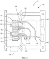
- a stamped contact leadframe or leadframe 60 such as used in a reel-to-reel manufacturing operation includes a suitable conductive material such as a conductive foil layer 41 of unitary construction including contacts 44 extending to contacts 18 via corresponding leads 62. That is, conductive signal leads 62 interconnect the signal contact pads 44 and contacts 18. Ground contacts 46 are positioned relative to contacts 44 as previously discussed. Carrier bars 66 of leadframe 60 are utilized in order to maintain the relative positions between stamped contacts 18, 44, 46 until after the protective housing 40 ( FIG. 4 ) is formed. To improve electrical conductivity, portions of contacts 44, 46 may include a plated region 64, such as with a thin layer of gold or other highly conductive material. As further shown in FIG.
- At least one of contacts 44, 46 may include a retention feature 68 ( FIG. 3 only shows retention feature 68 in contacts 46), such as a chamfer, such as a chamfered opening that is utilized to secure contacts 46 in physical contact with housing 40, as will be discussed in further detail below.
- the retention feature may be associated with a portion of the periphery of contacts 44, 46.
- protective dielectric housing 40 is selectively formed over opposed surfaces 71, 72 ( FIG. 4A ) of leadframe 60. More specifically, portion 74 of housing 40 embeds leads 62 ( FIG. 3 ) and portion 73 of housing 40 surrounds contacts 44, 46. That is, portion 73 is larger than and encompasses the collective footprint of contacts 44, 46 so as to protect the contacts in an unmated condition. For example, as shown in FIG.
- backplate mating edge 54 which similarly defines the edge of portion 73 of housing 40, extends in direction A further than any of the ends of contacts 44, 46, and frame portion 42 of connector module 38 extends both upwardly and downwardly in direction B that is perpendicular to direction A, with frame portion 42 generally surrounding and structurally protecting contacts 44, 46 in an unmated position.
- portion 73 of housing 40 is applied in contact with surface 72 of contacts 44, 46.
- the term "in contact” may include partially embedding the peripheral edges of contacts 44, 46 with portion 73 of housing 40.
- portion 73 of housing 40 is exposed or not covered with portion 73 of housing 40, such that surface 71 of the contacts can be connected to and form an electrical connection with a corresponding contact of another electrical connector as previously discussed.
- material of portion 73 of housing 40 is flowed onto retention feature 68 of contacts 46. That is, as material of portion 73 of housing 40 is flowed and brought into contact with surface 72 of contacts 44, 46, the material similarly flows through and onto the portion of retention feature 68 that is associated with surface 71, such as the chamfered portion of a chamfered opening of an exemplary embodiment of retention feature 68.
- portion 73 of housing 40 As a result, once the material of portion 73 of housing 40 has cured, the material of portion 73, for a retention feature 68 defining a chamfered opening, becomes the equivalent of a countersunk fastener head that secures surface 72 of contact 46 against or in contact with contact 46. That is, contact 46 is prevented from moving away from or becoming detached or delaminated from or relative to portion 73 of housing 40.
- FIGS. 5 and 5A show a stamped leadframe 70, similar to leadframe 60, which includes a suitable conductive material such as a conductive foil layer of unitary construction forming a commoning member or ground shield or plate ground member 76.
- Ground member 76 is secured in position by carrier bars 77 in a manner as previously discussed.
- a plurality of retention features 78, 79, 80 extend generally perpendicularly to the body of ground member 76 so as to extend into and engage corresponding retention features when assembled with connector module 38 ( FIG. 4 ).
- ground contacts or contacts 82 extend outwardly and are laterally offset from the body of ground member 76 so as to align with corresponding contacts 18 ( FIG. 4 ) of connector module 38 when assembled to the connector module.
- the connector module 38 of FIG. 2 shows contacts 18, 82.
- FIG. 6 shows ground member 76 removed from leadframe 70 ( FIG. 5 ).
- FIG. 7 shows module first side 50 of connector module 38 prior to assembly of ground member 76.
- FIG. 8 shows a module second side 51 opposite that of module first side 50, with ground member 76 positioned overlying one side of a portion 74 of housing 40 and retention features 78, 79, 80 engaged with their corresponding retention features of connector module 38. More specifically, as a result of retention features 78 of ground member 76 engaging with corresponding engagement features 53 of contact 46 ( FIG. 3 ), ground contacts or contacts 46 are in electrical communication with ground member 76, providing enhanced grounding capability by commoning the ground contacts.
- stamped layer 84 which is similar to stamped layer 41 of FIG. 3 , includes a ground member or ground bar 88 to which corresponding ends of ground contacts 86 are secured.
- Ground bar 88 is of unitary or one-piece construction with ground contacts 86.
- Ground bar 88 is rotated 180 degrees about an axis 100 that is transverse to ground contacts 86.
- Ground bar 88 is generally U-shaped, with parallel legs of the U-shaped ground bar extending generally parallel to and in protective close proximity to corresponding contacts 44, 86.
- ground bar 88 is arranged such that the ground bar not require rotation about the transverse axis 100, as the parallel legs of the ground bar are positioned in stamped layer 84 essentially as shown in FIG. 11 .
- ground bar 88 is at least partially surrounded by portion 73 of housing 40.
- FIGS. 13-15 Shown in FIGS. 13-15 , an alternate embodiment of an electrical connector 110 is now discussed.
- FIG. 14 which is a cross-section taken along line 14-14 of FIG. 13
- frame portion 42 of connector module 96 includes a notch 98 usable for providing an insertion/alignment feature of the connector.
- FIGS. 16-19 discuss an alternate embodiment of a housing 140 of an electrical connector using contact pairs for differential signaling, such as contact pairs 104, 106 ( FIG. 11 ).
- contact pairs 104, 106 as a result of the 90 degree turn within the right-angle connector, one leg (inner leg) of the contact pair is physically shorter than the other leg (outer leg), resulting in an electrical signal propagation delay or propagation delay, sometimes referred to as intra-pair skew or skew or jitter (transmission bandwidth decreases) through the legs of contact pairs 104, 106 between the input and output sides of the contact pairs. That is, as shown in FIGS. 16-17 for housing 120 ( FIG.
- the output signals from the inner and outer legs of respective contact pairs 104, 106 have a skew that is approximately equal to zero, or approximately ( ⁇ ) zero skew ( FIG. 19 ).
- electrical propagation delay features 124, 126 also referred to as skew flags, introduce an air pocket over a portion of each of the outer legs of respective contact pairs 104, 106, decreasing propagation delay of the outer legs (i.e., increasing velocity of signal propagation) due to lowering the relative permittivity.
- the electrical propagation delay features 124, 126 it is possible to size the electrical propagation delay features 124, 126 to achieve an intra-pair skew of approximately zero (pico-)seconds.
- introducing the air pocket increases the differential impedance between the inner and outer legs of the contact pairs, widening the portion of the outer leg exposed to the air pocket can restore the impedance balance.
- a method of forming a connector 10, such as by a reel-to-reel manufacturing process includes positioning a contact leadframe 60 of unitary construction including contacts 44 extending to second contacts 18 via corresponding leads 62, and forming a protective overmolded contact module housing 40 over the leadframe 60, forming a connector module 38, the housing 40 embedding the leads 62 and surrounding the contacts 44, the contacts 18 extending from the housing 40, with a side or surface 72 of the contacts 44 in contact with the housing 40, and an opposed side 71 or surface of the contacts 44 being exposed, and positioning a plurality of connector modules 38 in an aligned arrangement.
Landscapes
- Engineering & Computer Science (AREA)
- Manufacturing & Machinery (AREA)
- Details Of Connecting Devices For Male And Female Coupling (AREA)
Abstract
Description
- The present invention is directed to electrical connectors, and more particularly, to electrical connectors having a plurality of contacts protected by a plastic overmold in the unmated state.
- Some electrical connectors have a mating end wherein conductive terminals are exposed for engagement with the terminals of a mating connector. This is common in a right angled connector used for interconnecting circuit boards such as a back plane and a daughter board. The back plane typically has a connector, commonly referred to as a receptacle, that mates with a daughter board connector, commonly referred to as a header. Portions of the terminals in either the receptacle or header are often exposed for engagement with the terminals of the header connector.
- In at least some right angled receptacle connectors, the receptacle includes a plurality of wafers or exposed contact pins, each of which includes signal carrying traces and ground traces along with signal and ground contact pads. Applying these traces to wafers is expensive. Alternately, overmolding conductive stamped layers, sometimes referred to as leadframes, have been utilized in place of the wafers to manufacture these connectors. However, prior to mating with the daughter board, the exposed, elongated contacts of the connector are fragile and susceptible to damage.
- The problem to be solved is a need for a connector that addresses these shortcomings in a cost effective manner and without adding to the size or complexity of the connector.
- The solution is provided by an electrical connector including a contact leadframe of unitary construction including first contacts extending to second contacts via corresponding leads, and an overmolded contact module housing formed over the leadframe, forming a connector module. The connector further includes the housing embedding the leads and surrounding the first contacts, the second contacts extending from the housing. The connector further includes a first surface of the first contacts in contact with the housing, and an opposed second surface of the first contacts being exposed. The connector includes a plurality of connector modules positioned in an aligned arrangement.
- The invention will now be described by way of example with reference to the accompanying drawings in which:
-
FIG. 1 is a perspective view of an exemplary connector according to the present invention. -
FIG. 2 is a front perspective view of an exemplary connector module according to the present invention. -
FIG. 2A is a cross-section taken alonglines 2A-2A taken from the connector module ofFIG. 2 according to the present invention. -
FIG. 3 is a partial elevation view of an exemplary leadframe according to the present invention. -
FIG. 4 is a partial elevation view of the leadframe covered by an exemplary protective housing according to the present invention. -
FIG. 4A is an end view of the covered leadframe ofFIG. 4 according to the present invention. -
FIG. 5 is a partial elevation view of an exemplary leadframe of a ground member according to the present invention. -
FIG. 5A is an end view of the leadframe ofFIG. 5 according to the present invention. -
FIG. 6 is an elevation view of a freestanding ground member ofFIG. 5 according to the present invention. -
FIG. 7 is a freestanding leadframe covered by the protective housing ofFIG. 4 according to the present invention. -
FIG. 8 is the freestanding leadframe covered by the protective housing ofFIG. 7 rotated 180 degrees about a vertical axis according to the present invention. -
FIG. 9 is an upper perspective view of an exemplary clip according to the present invention. -
FIG. 10 is a lower perspective view of connector modules secured to the clip ofFIG. 9 according to the present invention. -
FIG. 11 is a perspective view of an exemplary freestanding leadframe according to the present invention. -
FIG. 12 is a partial elevation view of an exemplary connector module including the freestanding leadframe ofFIG. 11 according to the present invention. -
FIG. 13 is a perspective view of an exemplary connector according to the present invention. -
FIG. 14 is a cross-section taken along line 14-14 of the connector module ofFIG. 13 according to the present invention. -
FIG. 15 is a perspective view of a connector module ofFIG. 13 according to the present invention. -
FIG. 16 is an elevation view of an exemplary connector module according to the present invention. -
FIG. 17 is a graphical representation of input/output signals from a contact pair of the connector module ofFIG. 16 according to the present invention. -
FIG. 18 is an elevation view of an exemplary connector module according to the present invention. -
FIG. 19 is a graphical representation of input/output signals from a contact pair of the connector module ofFIG. 18 according to the present invention. - Wherever possible, the same reference numbers will be used throughout the drawings to represent the same parts.
- The description of illustrative embodiments according to principles of the present invention is intended to be read in connection with the accompanying drawings, which are to be considered part of the entire written description. Terms such as "attached," "affixed," "connected," "coupled," "interconnected," "engaged," "installed" and the like refer to a relationship wherein structures are secured or attached to one another either directly or indirectly through intervening structures, as well as both movable or rigid attachments or relationships, unless expressly described otherwise. Moreover, the features and benefits of the invention are illustrated by reference to the preferred embodiments. Accordingly, the invention expressly should not be limited to such preferred embodiments illustrating some possible non-limiting combination of features that may exist alone or in other combinations of features; the scope of the invention being defined by the claims appended hereto.
- An embodiment is directed to an electrical connector including a contact leadframe of unitary construction including first contacts extending to second contacts via corresponding leads, and an overmolded contact module housing formed over the leadframe, forming a connector module. The connector further includes the housing embedding the leads and surrounding the first contacts, the second contacts extending from the housing. The connector further includes a first surface of the first contacts in contact with the housing, and an opposed second surface of the first contacts being exposed. The connector includes a plurality of connector modules positioned in an aligned arrangement.
- A further embodiment is directed to an electrical connector includes a contact leadframe of unitary construction including first contacts extending to second contacts via corresponding signal leads and a third contact positioned in close proximity to the first contacts. The connector further includes an overmolded contact module housing formed over the leadframe, forming a connector module, the housing embedding the leads and surrounding the first contacts and the third contact, the second contacts extending from the housing. The connector further includes a first surface of each of the first contacts and the third contact in contact with the housing, and an opposed second surface of each of the first contacts and the third contact being exposed, and a ground member connected to the third contact. The connector includes a plurality of connector modules positioned in an aligned arrangement.
- A yet further embodiment is directed to a method of forming a connector includes positioning a contact leadframe of unitary construction including first contacts extending to second contacts via corresponding signal leads. The method further provides forming an overmolded contact module housing over the leadframe, forming a connector module, the housing embedding the leads and surrounding the first contacts, the second contacts extending from the housing, a first surface of the first contacts in contact with the housing, and an opposed second surface of the first contacts being exposed. The method further provides positioning a plurality of connector modules in an aligned arrangement.
-
FIG. 1 illustrates a perspective view of anelectrical connector 10 formed in accordance with an exemplary embodiment of the present invention. Theconnector 10 is a header connector that is configured to be mounted on acircuit board 12 which in an exemplary embodiment is a daughter board. As shown, theconnector 10 has amating face 14 and amounting interface 16 having outwardly extendingcontacts 18 for mounting theconnector 10 to thecircuit board 12. In an exemplary embodiment, themounting interface 16 is substantially perpendicular to themating face 14 such that theheader connector 10 interconnects electrical components that are substantially at a right angle to each other. Themating face 14 of theconnector 10 defines a back plane connector interface. In one embodiment, theconnector 10 may be used to interconnect a daughter board to a back plane circuit board. In other embodiments, theconnector 10 may be configured to interconnect electrical components that are at other than a right angle to each other. - While the invention will be described in terms of a connector carrying differential signals, it is to be understood that the following description is for illustrative purposes only and is but one potential application of the inventive concepts herein. It is appreciated that the benefits and advantages of the invention may accrue equally to other types of signal connectors and power connectors.
- The
connector 10 includes a dielectric overmoldedcontact module housing 20 that has anupper housing portion 22 and alower housing portion 24. Theupper housing portion 22 includes upper andlower shrouds mating face 14 of theconnector 10.Upper shroud 26 andlower shroud 28 extend forwardly fromupper housing portion 22 in the direction of arrow A, which is also the mating direction of theconnector 10.Upper housing portion 22 includes opposed ends 32, 34. Upper andlower housing portions connector modules 38 that are received intohousing 20 with a clip 90 (FIG. 9 ) that is part ofupper shroud 26 in one embodiment.Clip 90 includes a plurality ofslots 93 that help position and align theconnector modules 38 to facilitate mating with a mating connector (not shown inFIG. 1 ). -
Connector modules 38, sometimes referred to as chicklets or chicklet assemblies, include signal or power contacts or contact pads orcontacts 44 and ground contact pads or contacts orground contacts 46.Ground contacts 46 have a length measured in the direction of arrow A that is greater than a corresponding length of thesignal contacts 44. In one embodiment, theconnector 10 is a high speed connector that carries differential signals and thesignal contacts 44 andground contacts 46 are arranged in an alternating pattern wherein pairs ofsignal contacts 44 are separated by aground contact 46. For instance, as shown inFIG. 1 for theexemplary connector module 38 temporarily extracted fromconnector 10 for purposes of discussion, theconnector module 38 starts at the bottom with aground contact 46 adjacent thelower shroud 28 and extends upwardly to a pair ofsignal contacts 44 adjacent thelower shroud 28, followed by a generally centrally positionedground contact 46, further extending upwardly to another pair ofsignal contacts 44 adjacentupper shroud 26, ending at the top with anotherground contact 46 adjacent theupper shroud 26. In one embodiment, the arrangement ofcontacts contacts different connector modules 38, such as adjacent connector modules ofconnector 10. Theconnector 10 is modular in construction and in the embodiment shown inFIG. 1 includes 26connector modules 38 with a total of 52 differential signal pairs of contacts and four modules that deliver power. It is to be understood that in alternative embodiments, a greater or fewer number of theconnector modules 38 may be used, and that the connector modules may be configured with a different number of differential signal pairs. Theconnector modules 38 project from theshrouds ground contacts 46 is to provide electrostatic discharge (ESD) protection for thesignal contacts 44 as discussed in additional detail in Applicant's United States Patent No.7,044,794 entitled "Electrical Connector with ESD Protection," which is hereby incorporated by reference in its entirety. -
FIG. 2 is an elevation perspective view of anexemplary connector module 38 illustrating a modulefirst side 50.Connector module 38 includes a protective overmolded contact module housing orhousing 40 having aframe portion 42. At least a segment offrame portion 42 has a predeterminedthickness 48 helping to maintain a desired separation or spacing betweenadjacent connector modules 38. When a plurality ofconnector modules 38 are collectively arranged between upper andlower shrouds FIG. 1 , collectively theframe portions 42 define acontinuous shroud structure 102.Frame portion 42 includes anengagement feature 43, such as a pair of undercuts 45 (FIG. 2A ) which engagement feature 43 is slidably received byslot 93 formed inleg 91 of clip 90 (FIG. 9 ) of upper shroud 26 (FIG. 1 ).Clip 90 includes asecond leg 92 extending generally perpendicular toleg 91.Leg 91 includesopenings 94 for receiving engagement features 47 formed inframe portion 42. As a result ofslot 93 andopenings 94 ofclip 90 receiving corresponding engagement features 43, 47 offrame portion 42,clip 90 is thereby secured toconnector module 38.FIG. 10 shows a plurality ofconnector modules 38 secured in corresponding engagement features ofclip 90.Connector module 38 includes amating end 52 that has a forward mating edge or backplane edge 54. Themating end 52 is configured to mate with a mating connector which may be a back plane connector (not shown inFIG. 2 ). Theconnector module 38 also includes a mounting edge ordaughter board edge 56 through which extendcontacts 18 in the lower housing 24 (FIG. 1 ) at the interface with the circuit board 12 (FIG. 1 ). The mountingedge 56 is substantially perpendicular to themating edge 54. Theconnector module 38 has chamferedcorners 58 at themating end 52 to facilitate the mating process with the mating connector. - In an exemplary embodiment, as shown in
FIG. 3 , a stamped contact leadframe orleadframe 60, such as used in a reel-to-reel manufacturing operation includes a suitable conductive material such as aconductive foil layer 41 of unitaryconstruction including contacts 44 extending tocontacts 18 via corresponding leads 62. That is, conductive signal leads 62 interconnect thesignal contact pads 44 andcontacts 18.Ground contacts 46 are positioned relative tocontacts 44 as previously discussed. Carrier bars 66 ofleadframe 60 are utilized in order to maintain the relative positions between stampedcontacts FIG. 4 ) is formed. To improve electrical conductivity, portions ofcontacts region 64, such as with a thin layer of gold or other highly conductive material. As further shown inFIG. 3 , at least one ofcontacts FIG. 3 only showsretention feature 68 in contacts 46), such as a chamfer, such as a chamfered opening that is utilized to securecontacts 46 in physical contact withhousing 40, as will be discussed in further detail below. In one embodiment, the retention feature may be associated with a portion of the periphery ofcontacts - As shown in
FIGS. 4 and 4A , protectivedielectric housing 40 is selectively formed overopposed surfaces 71, 72 (FIG. 4A ) ofleadframe 60. More specifically,portion 74 ofhousing 40 embeds leads 62 (FIG. 3 ) andportion 73 ofhousing 40 surroundscontacts portion 73 is larger than and encompasses the collective footprint ofcontacts FIG. 2 ,backplate mating edge 54, which similarly defines the edge ofportion 73 ofhousing 40, extends in direction A further than any of the ends ofcontacts frame portion 42 ofconnector module 38 extends both upwardly and downwardly in direction B that is perpendicular to direction A, withframe portion 42 generally surrounding and structurally protectingcontacts housing 40 overleadframe 60,portion 73 ofhousing 40 is applied in contact withsurface 72 ofcontacts contacts portion 73 ofhousing 40. However,surface 71 ofcontacts portion 73 ofhousing 40, such thatsurface 71 of the contacts can be connected to and form an electrical connection with a corresponding contact of another electrical connector as previously discussed. Essentially simultaneously, material ofportion 73 ofhousing 40 is flowed ontoretention feature 68 ofcontacts 46. That is, as material ofportion 73 ofhousing 40 is flowed and brought into contact withsurface 72 ofcontacts retention feature 68 that is associated withsurface 71, such as the chamfered portion of a chamfered opening of an exemplary embodiment ofretention feature 68. As a result, once the material ofportion 73 ofhousing 40 has cured, the material ofportion 73, for aretention feature 68 defining a chamfered opening, becomes the equivalent of a countersunk fastener head that securessurface 72 ofcontact 46 against or in contact withcontact 46. That is,contact 46 is prevented from moving away from or becoming detached or delaminated from or relative toportion 73 ofhousing 40. -
FIGS. 5 and 5A show astamped leadframe 70, similar toleadframe 60, which includes a suitable conductive material such as a conductive foil layer of unitary construction forming a commoning member or ground shield orplate ground member 76.Ground member 76 is secured in position bycarrier bars 77 in a manner as previously discussed. A plurality of retention features 78, 79, 80 extend generally perpendicularly to the body ofground member 76 so as to extend into and engage corresponding retention features when assembled with connector module 38 (FIG. 4 ). Additionally, ground contacts orcontacts 82 extend outwardly and are laterally offset from the body ofground member 76 so as to align with corresponding contacts 18 (FIG. 4 ) ofconnector module 38 when assembled to the connector module. For example, theconnector module 38 ofFIG. 2 showscontacts -
FIG. 6 showsground member 76 removed from leadframe 70 (FIG. 5 ).FIG. 7 shows modulefirst side 50 ofconnector module 38 prior to assembly ofground member 76.FIG. 8 shows a modulesecond side 51 opposite that of modulefirst side 50, withground member 76 positioned overlying one side of aportion 74 ofhousing 40 and retention features 78, 79, 80 engaged with their corresponding retention features ofconnector module 38. More specifically, as a result of retention features 78 ofground member 76 engaging with corresponding engagement features 53 of contact 46 (FIG. 3 ), ground contacts orcontacts 46 are in electrical communication withground member 76, providing enhanced grounding capability by commoning the ground contacts.U.S. Patent Nos. 7,637,767 titled CABLE CONNECTOR ASSEMBLY and7,566,247 titled SKEW CONTROLLED LEADRAME FOR A CONTACT MODULE ASSEMBLY, each issued to Applicant, further discussing commoning members (e.g.,FIG. 5 andFIG. 7 , respectively) and corresponding structure are incorporated by reference in their entirety. - As shown in
FIG. 11 , stampedlayer 84, which is similar to stampedlayer 41 ofFIG. 3 , includes a ground member orground bar 88 to which corresponding ends ofground contacts 86 are secured.Ground bar 88 is of unitary or one-piece construction withground contacts 86.Ground bar 88 is rotated 180 degrees about anaxis 100 that is transverse to groundcontacts 86.Ground bar 88 is generally U-shaped, with parallel legs of the U-shaped ground bar extending generally parallel to and in protective close proximity tocorresponding contacts ground bar 88 is arranged such that the ground bar not require rotation about thetransverse axis 100, as the parallel legs of the ground bar are positioned in stampedlayer 84 essentially as shown inFIG. 11 . In one embodiment, at least the region of theground bar 88 alongaxis 100 contains a joggle. As shown,contacts U-shaped ground bar 88. This ground bar construction effects an electrostatic discharge strip to the front of the connector (i.e., opposite pins 18), as well as adding strength, rigidity and protective capability to the resulting connector. As further shown inFIG. 12 ,ground bar 88 is at least partially surrounded byportion 73 ofhousing 40. - Shown in
FIGS. 13-15 , an alternate embodiment of anelectrical connector 110 is now discussed. As shown inFIG. 14 , which is a cross-section taken along line 14-14 ofFIG. 13 ,frame portion 42 ofconnector module 96 includes anotch 98 usable for providing an insertion/alignment feature of the connector. -
FIGS. 16-19 discuss an alternate embodiment of ahousing 140 of an electrical connector using contact pairs for differential signaling, such as contact pairs 104, 106 (FIG. 11 ). For such contact pairs 104, 106, as a result of the 90 degree turn within the right-angle connector, one leg (inner leg) of the contact pair is physically shorter than the other leg (outer leg), resulting in an electrical signal propagation delay or propagation delay, sometimes referred to as intra-pair skew or skew or jitter (transmission bandwidth decreases) through the legs of contact pairs 104, 106 between the input and output sides of the contact pairs. That is, as shown inFIGS. 16-17 for housing 120 (FIG. 16 ), while an input signal to the inner and outer legs of contact pairs 104, 106 has zero skew (FIG. 17 ), the output signal from the inner and outer legs of contact pairs 104, 106 has a non-zero skew (FIG. 17 ), which is undesirable. - In contrast, as shown in
FIGS. 18-19 for housing 140 (FIG. 16 ), as a result of the addition of electrical propagation delay features 124, 126, the output signals from the inner and outer legs of respective contact pairs 104, 106 have a skew that is approximately equal to zero, or approximately (∼) zero skew (FIG. 19 ). As shown inFIG. 18 electrical propagation delay features 124, 126, also referred to as skew flags, introduce an air pocket over a portion of each of the outer legs of respective contact pairs 104, 106, decreasing propagation delay of the outer legs (i.e., increasing velocity of signal propagation) due to lowering the relative permittivity. As a result, it is possible to size the electrical propagation delay features 124, 126 to achieve an intra-pair skew of approximately zero (pico-)seconds. Although introducing the air pocket increases the differential impedance between the inner and outer legs of the contact pairs, widening the portion of the outer leg exposed to the air pocket can restore the impedance balance. - As appreciated by one having ordinary skill in the art, a method of forming a
connector 10, such as by a reel-to-reel manufacturing process includes positioning acontact leadframe 60 of unitaryconstruction including contacts 44 extending tosecond contacts 18 via corresponding leads 62, and forming a protective overmoldedcontact module housing 40 over theleadframe 60, forming aconnector module 38, thehousing 40 embedding theleads 62 and surrounding thecontacts 44, thecontacts 18 extending from thehousing 40, with a side orsurface 72 of thecontacts 44 in contact with thehousing 40, and anopposed side 71 or surface of thecontacts 44 being exposed, and positioning a plurality ofconnector modules 38 in an aligned arrangement.
Claims (16)
- An electrical connector (10) comprising:a contact leadframe (60) of unitary construction including first contacts (44) extending to second contacts (18) via corresponding leads (62); and an overmolded contact module housing (40) formed over the leadframe (60), forming a connector module (38), the housing (40) embedding the leads (62) and surrounding the first contacts (44), the second contacts (18) extending from the housing (40), a first surface (72) of the first contacts (44) in contact with the housing (40), and an opposed second surface (71) of the first contacts (44) being exposed;wherein the connector (10) includes a plurality of connector modules (38) positioned in an aligned arrangement.
- The electrical connector (10) of claim 1 further comprisesat least one third contact (46) positioned in close proximity to the first contacts (44) and surrounded by the housing (40), a first surface (72) of the at least one third contact (46) in contact with the housing (40), and an opposed second surface (71) of the at least one third contact (46) being exposed; anda ground member (76) connected to the at least one third contact (46).
- The electrical connector (10) of claim 2, wherein the ground member (76) is positioned overlying one surface of a portion of the housing (40).
- The electrical connector (10) of claim 2 or 3, wherein the ground member (76) is a plate.
- The electrical connector (10) of claim 2, 3 or 4, wherein the ground member (76) is a separate component from the leadframe (60), secured to the at least one third contact (46), and at least partially surrounded by the housing (40).
- The electrical connector (10) of any preceding claim, wherein at least one said contact (18, 44, 46) has a retention feature (68), the retention feature (68) retaining housing material flowed onto the retention feature (68) from the first surface (72) of the at least one contact (18, 44, 46), thereby preventing the first surface (72) of the at least one contact (18, 44, 46) from moving away from the housing (40).
- The electrical connector (10) of claim 6, wherein the retention feature (68) is a chamfer.
- The electrical connector (10) of any preceding claim, wherein the leadframe further comprises a generally U-shaped ground bar (88).
- The electrical connector (10) of any preceding claim, wherein the housing (40) includes a frame portion (42) having a predetermined thickness (48).
- The electrical connector (10) of claim 9, wherein the frame portion (42) includes a first engagement feature (43).
- The electrical connector (10) of claim 10, wherein the frame portion (42) includes a second engagement feature (47).
- The electrical connector (10) of claim 10 or 11 further comprising a clip (90) having a first leg (91) and a second leg (91), the first leg (91) having a slot (93) to slidably receive the first engagement feature (43).
- The electrical connector (10) of claims 11 and 12, wherein the second leg (92) has an opening (94) to receive the second engagement feature (47).
- The electrical connector (10) of claim 9, wherein the frame portion (42) has a notch (98).
- The electrical connector (10) of claim 9, wherein collectively, the frame portions (42) of the housings (40) of the plurality of arranged connector modules (38) define a continuous shroud structure (102).
- The electrical connector (10) of claim 1, wherein the housing (140) further comprises an electrical signal propagation delay feature (124, 126).
Applications Claiming Priority (1)
| Application Number | Priority Date | Filing Date | Title |
|---|---|---|---|
| US15/730,982 US10535971B2 (en) | 2017-10-12 | 2017-10-12 | Electrical connector |
Publications (2)
| Publication Number | Publication Date |
|---|---|
| EP3471216A1 true EP3471216A1 (en) | 2019-04-17 |
| EP3471216B1 EP3471216B1 (en) | 2021-01-06 |
Family
ID=63832225
Family Applications (1)
| Application Number | Title | Priority Date | Filing Date |
|---|---|---|---|
| EP18199380.9A Active EP3471216B1 (en) | 2017-10-12 | 2018-10-09 | Electrical connector |
Country Status (2)
| Country | Link |
|---|---|
| US (1) | US10535971B2 (en) |
| EP (1) | EP3471216B1 (en) |
Families Citing this family (8)
| Publication number | Priority date | Publication date | Assignee | Title |
|---|---|---|---|---|
| US10535971B2 (en) * | 2017-10-12 | 2020-01-14 | Te Connectivity Corporation | Electrical connector |
| CN111490380B (en) * | 2019-03-30 | 2021-10-26 | 富士康(昆山)电脑接插件有限公司 | Electrical connector |
| US11264749B2 (en) | 2020-03-26 | 2022-03-01 | TE Connectivity Services Gmbh | Modular connector with printed circuit board wafer to reduce crosstalk |
| US11297712B2 (en) | 2020-03-26 | 2022-04-05 | TE Connectivity Services Gmbh | Modular printed circuit board wafer connector with reduced crosstalk |
| US11031734B1 (en) | 2020-03-26 | 2021-06-08 | TE Connectivity Services Gmbh | Modular electrical connector with reduced crosstalk |
| US11025014B1 (en) | 2020-03-26 | 2021-06-01 | TE CONNECTNITY SERVICES GmbH | Shield component for use with modular electrical connector to reduce crosstalk |
| US10965062B1 (en) | 2020-03-26 | 2021-03-30 | TE Connectivity Services Gmbh | Modular electrical connector with conductive coating to reduce crosstalk |
| US10998678B1 (en) | 2020-03-26 | 2021-05-04 | TE Connectivity Services Gmbh | Modular electrical connector with additional grounding |
Citations (9)
| Publication number | Priority date | Publication date | Assignee | Title |
|---|---|---|---|---|
| US20020098738A1 (en) * | 2001-01-25 | 2002-07-25 | Astbury Allan L. | Connector molding method and shielded waferized connector made therefrom |
| US6471549B1 (en) * | 1999-10-18 | 2002-10-29 | Lappoehn Juergen | Shielded plug-in connector |
| US20050070160A1 (en) * | 2003-09-30 | 2005-03-31 | Cohen Thomas S. | High speed, high density electrical connector assembly |
| US7044794B2 (en) | 2004-07-14 | 2006-05-16 | Tyco Electronics Corporation | Electrical connector with ESD protection |
| US20070155241A1 (en) * | 2005-12-31 | 2007-07-05 | Erni Elektroapparate Gmbh | Plug-and-socket connector |
| US20080203547A1 (en) * | 2007-02-26 | 2008-08-28 | Minich Steven E | Insert molded leadframe assembly |
| US7637767B2 (en) | 2008-01-04 | 2009-12-29 | Tyco Electronics Corporation | Cable connector assembly |
| US20140273557A1 (en) * | 2013-03-13 | 2014-09-18 | Amphenol Corporation | Housing for a high speed electrical connector |
| US20140322985A1 (en) * | 2008-01-17 | 2014-10-30 | Amphenol Corporation | Electrical connector assembly |
Family Cites Families (5)
| Publication number | Priority date | Publication date | Assignee | Title |
|---|---|---|---|---|
| US7172461B2 (en) | 2004-07-22 | 2007-02-06 | Tyco Electronics Corporation | Electrical connector |
| US7566247B2 (en) | 2007-06-25 | 2009-07-28 | Tyco Electronics Corporation | Skew controlled leadframe for a contact module assembly |
| US9455545B2 (en) * | 2013-03-13 | 2016-09-27 | Amphenol Corporation | Lead frame for a high speed electrical connector |
| CN106207569B (en) * | 2016-07-29 | 2019-04-19 | 中航光电科技股份有限公司 | High-speed electrical connector and its signal module and method for forming the signal module |
| US10535971B2 (en) * | 2017-10-12 | 2020-01-14 | Te Connectivity Corporation | Electrical connector |
-
2017
- 2017-10-12 US US15/730,982 patent/US10535971B2/en active Active
-
2018
- 2018-10-09 EP EP18199380.9A patent/EP3471216B1/en active Active
Patent Citations (9)
| Publication number | Priority date | Publication date | Assignee | Title |
|---|---|---|---|---|
| US6471549B1 (en) * | 1999-10-18 | 2002-10-29 | Lappoehn Juergen | Shielded plug-in connector |
| US20020098738A1 (en) * | 2001-01-25 | 2002-07-25 | Astbury Allan L. | Connector molding method and shielded waferized connector made therefrom |
| US20050070160A1 (en) * | 2003-09-30 | 2005-03-31 | Cohen Thomas S. | High speed, high density electrical connector assembly |
| US7044794B2 (en) | 2004-07-14 | 2006-05-16 | Tyco Electronics Corporation | Electrical connector with ESD protection |
| US20070155241A1 (en) * | 2005-12-31 | 2007-07-05 | Erni Elektroapparate Gmbh | Plug-and-socket connector |
| US20080203547A1 (en) * | 2007-02-26 | 2008-08-28 | Minich Steven E | Insert molded leadframe assembly |
| US7637767B2 (en) | 2008-01-04 | 2009-12-29 | Tyco Electronics Corporation | Cable connector assembly |
| US20140322985A1 (en) * | 2008-01-17 | 2014-10-30 | Amphenol Corporation | Electrical connector assembly |
| US20140273557A1 (en) * | 2013-03-13 | 2014-09-18 | Amphenol Corporation | Housing for a high speed electrical connector |
Also Published As
| Publication number | Publication date |
|---|---|
| US10535971B2 (en) | 2020-01-14 |
| EP3471216B1 (en) | 2021-01-06 |
| US20190115709A1 (en) | 2019-04-18 |
Similar Documents
| Publication | Publication Date | Title |
|---|---|---|
| EP3471216B1 (en) | Electrical connector | |
| US10361520B2 (en) | High density electrical connector with shield plate louvers | |
| TWI583067B (en) | Electrical connector system | |
| US8062070B2 (en) | Connector assembly having a compensation circuit component | |
| JP4221466B2 (en) | Connector molding method and shielded wafer type connector made by the same method | |
| CN105191003B (en) | Housing for high-speed electrical connectors | |
| TWI424638B (en) | Performance enhancing contact module assemblies | |
| US9419360B2 (en) | Mating interfaces for high speed high density electrical connectors | |
| EP2209170B1 (en) | Orthogonal connector system | |
| TWI505569B (en) | High density connector assembly | |
| TWI527322B (en) | Grounding structures for header and receptacle assemblies | |
| US8157591B2 (en) | Electrical connector system | |
| US20110287663A1 (en) | Electrical connector incorporating circuit elements | |
| CN103779733B (en) | Ground connection inlay for the contact module of jack assemblies | |
| US8187034B2 (en) | Electrical connector system | |
| WO2016003663A1 (en) | Electrical connector with ground bus | |
| CN101803120A (en) | Backplane connector with improved pin header | |
| CN104300253B (en) | For transmitting the electric connector of data-signal | |
| EP2983252A1 (en) | Connector assembly having conductive holder members | |
| CN105210238B (en) | Lead frame for high-speed electrical connectors | |
| TWI519011B (en) | Electrical connector system | |
| CN105098515A (en) | Interlayer type plug connector | |
| CN102255180B (en) | Electrical connector system | |
| US8974253B2 (en) | Contact module for a receptacle assembly | |
| CN111834824A (en) | Receptacle connector with ground bus connector |
Legal Events
| Date | Code | Title | Description |
|---|---|---|---|
| PUAI | Public reference made under article 153(3) epc to a published international application that has entered the european phase |
Free format text: ORIGINAL CODE: 0009012 |
|
| STAA | Information on the status of an ep patent application or granted ep patent |
Free format text: STATUS: THE APPLICATION HAS BEEN PUBLISHED |
|
| AK | Designated contracting states |
Kind code of ref document: A1 Designated state(s): AL AT BE BG CH CY CZ DE DK EE ES FI FR GB GR HR HU IE IS IT LI LT LU LV MC MK MT NL NO PL PT RO RS SE SI SK SM TR |
|
| AX | Request for extension of the european patent |
Extension state: BA ME |
|
| STAA | Information on the status of an ep patent application or granted ep patent |
Free format text: STATUS: REQUEST FOR EXAMINATION WAS MADE |
|
| 17P | Request for examination filed |
Effective date: 20191008 |
|
| RBV | Designated contracting states (corrected) |
Designated state(s): AL AT BE BG CH CY CZ DE DK EE ES FI FR GB GR HR HU IE IS IT LI LT LU LV MC MK MT NL NO PL PT RO RS SE SI SK SM TR |
|
| STAA | Information on the status of an ep patent application or granted ep patent |
Free format text: STATUS: EXAMINATION IS IN PROGRESS |
|
| 17Q | First examination report despatched |
Effective date: 20191203 |
|
| REG | Reference to a national code |
Ref country code: DE Ref legal event code: R079 Ref document number: 602018011532 Country of ref document: DE Free format text: PREVIOUS MAIN CLASS: H01R0013405000 Ipc: H01R0013648000 |
|
| RIC1 | Information provided on ipc code assigned before grant |
Ipc: H01R 13/405 20060101ALI20200916BHEP Ipc: H01R 13/648 20060101AFI20200916BHEP Ipc: H01R 13/6587 20110101ALI20200916BHEP Ipc: H01R 13/514 20060101ALI20200916BHEP Ipc: H01R 13/518 20060101ALI20200916BHEP |
|
| GRAP | Despatch of communication of intention to grant a patent |
Free format text: ORIGINAL CODE: EPIDOSNIGR1 |
|
| STAA | Information on the status of an ep patent application or granted ep patent |
Free format text: STATUS: GRANT OF PATENT IS INTENDED |
|
| INTG | Intention to grant announced |
Effective date: 20201023 |
|
| GRAS | Grant fee paid |
Free format text: ORIGINAL CODE: EPIDOSNIGR3 |
|
| GRAA | (expected) grant |
Free format text: ORIGINAL CODE: 0009210 |
|
| STAA | Information on the status of an ep patent application or granted ep patent |
Free format text: STATUS: THE PATENT HAS BEEN GRANTED |
|
| AK | Designated contracting states |
Kind code of ref document: B1 Designated state(s): AL AT BE BG CH CY CZ DE DK EE ES FI FR GB GR HR HU IE IS IT LI LT LU LV MC MK MT NL NO PL PT RO RS SE SI SK SM TR |
|
| REG | Reference to a national code |
Ref country code: GB Ref legal event code: FG4D |
|
| REG | Reference to a national code |
Ref country code: AT Ref legal event code: REF Ref document number: 1353393 Country of ref document: AT Kind code of ref document: T Effective date: 20210115 Ref country code: CH Ref legal event code: EP |
|
| REG | Reference to a national code |
Ref country code: DE Ref legal event code: R096 Ref document number: 602018011532 Country of ref document: DE |
|
| REG | Reference to a national code |
Ref country code: IE Ref legal event code: FG4D |
|
| REG | Reference to a national code |
Ref country code: NL Ref legal event code: MP Effective date: 20210106 |
|
| REG | Reference to a national code |
Ref country code: AT Ref legal event code: MK05 Ref document number: 1353393 Country of ref document: AT Kind code of ref document: T Effective date: 20210106 |
|
| REG | Reference to a national code |
Ref country code: LT Ref legal event code: MG9D |
|
| PG25 | Lapsed in a contracting state [announced via postgrant information from national office to epo] |
Ref country code: NO Free format text: LAPSE BECAUSE OF FAILURE TO SUBMIT A TRANSLATION OF THE DESCRIPTION OR TO PAY THE FEE WITHIN THE PRESCRIBED TIME-LIMIT Effective date: 20210406 Ref country code: PT Free format text: LAPSE BECAUSE OF FAILURE TO SUBMIT A TRANSLATION OF THE DESCRIPTION OR TO PAY THE FEE WITHIN THE PRESCRIBED TIME-LIMIT Effective date: 20210506 Ref country code: LT Free format text: LAPSE BECAUSE OF FAILURE TO SUBMIT A TRANSLATION OF THE DESCRIPTION OR TO PAY THE FEE WITHIN THE PRESCRIBED TIME-LIMIT Effective date: 20210106 Ref country code: GR Free format text: LAPSE BECAUSE OF FAILURE TO SUBMIT A TRANSLATION OF THE DESCRIPTION OR TO PAY THE FEE WITHIN THE PRESCRIBED TIME-LIMIT Effective date: 20210407 Ref country code: HR Free format text: LAPSE BECAUSE OF FAILURE TO SUBMIT A TRANSLATION OF THE DESCRIPTION OR TO PAY THE FEE WITHIN THE PRESCRIBED TIME-LIMIT Effective date: 20210106 Ref country code: FI Free format text: LAPSE BECAUSE OF FAILURE TO SUBMIT A TRANSLATION OF THE DESCRIPTION OR TO PAY THE FEE WITHIN THE PRESCRIBED TIME-LIMIT Effective date: 20210106 Ref country code: BG Free format text: LAPSE BECAUSE OF FAILURE TO SUBMIT A TRANSLATION OF THE DESCRIPTION OR TO PAY THE FEE WITHIN THE PRESCRIBED TIME-LIMIT Effective date: 20210406 |
|
| PG25 | Lapsed in a contracting state [announced via postgrant information from national office to epo] |
Ref country code: SE Free format text: LAPSE BECAUSE OF FAILURE TO SUBMIT A TRANSLATION OF THE DESCRIPTION OR TO PAY THE FEE WITHIN THE PRESCRIBED TIME-LIMIT Effective date: 20210106 Ref country code: RS Free format text: LAPSE BECAUSE OF FAILURE TO SUBMIT A TRANSLATION OF THE DESCRIPTION OR TO PAY THE FEE WITHIN THE PRESCRIBED TIME-LIMIT Effective date: 20210106 Ref country code: LV Free format text: LAPSE BECAUSE OF FAILURE TO SUBMIT A TRANSLATION OF THE DESCRIPTION OR TO PAY THE FEE WITHIN THE PRESCRIBED TIME-LIMIT Effective date: 20210106 Ref country code: PL Free format text: LAPSE BECAUSE OF FAILURE TO SUBMIT A TRANSLATION OF THE DESCRIPTION OR TO PAY THE FEE WITHIN THE PRESCRIBED TIME-LIMIT Effective date: 20210106 Ref country code: AT Free format text: LAPSE BECAUSE OF FAILURE TO SUBMIT A TRANSLATION OF THE DESCRIPTION OR TO PAY THE FEE WITHIN THE PRESCRIBED TIME-LIMIT Effective date: 20210106 |
|
| PG25 | Lapsed in a contracting state [announced via postgrant information from national office to epo] |
Ref country code: IS Free format text: LAPSE BECAUSE OF FAILURE TO SUBMIT A TRANSLATION OF THE DESCRIPTION OR TO PAY THE FEE WITHIN THE PRESCRIBED TIME-LIMIT Effective date: 20210506 |
|
| REG | Reference to a national code |
Ref country code: DE Ref legal event code: R097 Ref document number: 602018011532 Country of ref document: DE |
|
| PG25 | Lapsed in a contracting state [announced via postgrant information from national office to epo] |
Ref country code: SM Free format text: LAPSE BECAUSE OF FAILURE TO SUBMIT A TRANSLATION OF THE DESCRIPTION OR TO PAY THE FEE WITHIN THE PRESCRIBED TIME-LIMIT Effective date: 20210106 Ref country code: CZ Free format text: LAPSE BECAUSE OF FAILURE TO SUBMIT A TRANSLATION OF THE DESCRIPTION OR TO PAY THE FEE WITHIN THE PRESCRIBED TIME-LIMIT Effective date: 20210106 Ref country code: EE Free format text: LAPSE BECAUSE OF FAILURE TO SUBMIT A TRANSLATION OF THE DESCRIPTION OR TO PAY THE FEE WITHIN THE PRESCRIBED TIME-LIMIT Effective date: 20210106 |
|
| PLBE | No opposition filed within time limit |
Free format text: ORIGINAL CODE: 0009261 |
|
| STAA | Information on the status of an ep patent application or granted ep patent |
Free format text: STATUS: NO OPPOSITION FILED WITHIN TIME LIMIT |
|
| PG25 | Lapsed in a contracting state [announced via postgrant information from national office to epo] |
Ref country code: DK Free format text: LAPSE BECAUSE OF FAILURE TO SUBMIT A TRANSLATION OF THE DESCRIPTION OR TO PAY THE FEE WITHIN THE PRESCRIBED TIME-LIMIT Effective date: 20210106 Ref country code: SK Free format text: LAPSE BECAUSE OF FAILURE TO SUBMIT A TRANSLATION OF THE DESCRIPTION OR TO PAY THE FEE WITHIN THE PRESCRIBED TIME-LIMIT Effective date: 20210106 Ref country code: RO Free format text: LAPSE BECAUSE OF FAILURE TO SUBMIT A TRANSLATION OF THE DESCRIPTION OR TO PAY THE FEE WITHIN THE PRESCRIBED TIME-LIMIT Effective date: 20210106 |
|
| 26N | No opposition filed |
Effective date: 20211007 |
|
| PG25 | Lapsed in a contracting state [announced via postgrant information from national office to epo] |
Ref country code: ES Free format text: LAPSE BECAUSE OF FAILURE TO SUBMIT A TRANSLATION OF THE DESCRIPTION OR TO PAY THE FEE WITHIN THE PRESCRIBED TIME-LIMIT Effective date: 20210106 Ref country code: AL Free format text: LAPSE BECAUSE OF FAILURE TO SUBMIT A TRANSLATION OF THE DESCRIPTION OR TO PAY THE FEE WITHIN THE PRESCRIBED TIME-LIMIT Effective date: 20210106 |
|
| PG25 | Lapsed in a contracting state [announced via postgrant information from national office to epo] |
Ref country code: SI Free format text: LAPSE BECAUSE OF FAILURE TO SUBMIT A TRANSLATION OF THE DESCRIPTION OR TO PAY THE FEE WITHIN THE PRESCRIBED TIME-LIMIT Effective date: 20210106 |
|
| PG25 | Lapsed in a contracting state [announced via postgrant information from national office to epo] |
Ref country code: IT Free format text: LAPSE BECAUSE OF FAILURE TO SUBMIT A TRANSLATION OF THE DESCRIPTION OR TO PAY THE FEE WITHIN THE PRESCRIBED TIME-LIMIT Effective date: 20210106 |
|
| REG | Reference to a national code |
Ref country code: CH Ref legal event code: PL |
|
| PG25 | Lapsed in a contracting state [announced via postgrant information from national office to epo] |
Ref country code: IS Free format text: LAPSE BECAUSE OF FAILURE TO SUBMIT A TRANSLATION OF THE DESCRIPTION OR TO PAY THE FEE WITHIN THE PRESCRIBED TIME-LIMIT Effective date: 20210506 |
|
| REG | Reference to a national code |
Ref country code: BE Ref legal event code: MM Effective date: 20211031 |
|
| PG25 | Lapsed in a contracting state [announced via postgrant information from national office to epo] |
Ref country code: MC Free format text: LAPSE BECAUSE OF FAILURE TO SUBMIT A TRANSLATION OF THE DESCRIPTION OR TO PAY THE FEE WITHIN THE PRESCRIBED TIME-LIMIT Effective date: 20210106 |
|
| PG25 | Lapsed in a contracting state [announced via postgrant information from national office to epo] |
Ref country code: LU Free format text: LAPSE BECAUSE OF NON-PAYMENT OF DUE FEES Effective date: 20211009 Ref country code: BE Free format text: LAPSE BECAUSE OF NON-PAYMENT OF DUE FEES Effective date: 20211031 |
|
| PG25 | Lapsed in a contracting state [announced via postgrant information from national office to epo] |
Ref country code: LI Free format text: LAPSE BECAUSE OF NON-PAYMENT OF DUE FEES Effective date: 20211031 Ref country code: CH Free format text: LAPSE BECAUSE OF NON-PAYMENT OF DUE FEES Effective date: 20211031 |
|
| PG25 | Lapsed in a contracting state [announced via postgrant information from national office to epo] |
Ref country code: IE Free format text: LAPSE BECAUSE OF NON-PAYMENT OF DUE FEES Effective date: 20211009 |
|
| PG25 | Lapsed in a contracting state [announced via postgrant information from national office to epo] |
Ref country code: NL Free format text: LAPSE BECAUSE OF NON-PAYMENT OF DUE FEES Effective date: 20210206 Ref country code: CY Free format text: LAPSE BECAUSE OF FAILURE TO SUBMIT A TRANSLATION OF THE DESCRIPTION OR TO PAY THE FEE WITHIN THE PRESCRIBED TIME-LIMIT Effective date: 20210106 |
|
| PG25 | Lapsed in a contracting state [announced via postgrant information from national office to epo] |
Ref country code: HU Free format text: LAPSE BECAUSE OF FAILURE TO SUBMIT A TRANSLATION OF THE DESCRIPTION OR TO PAY THE FEE WITHIN THE PRESCRIBED TIME-LIMIT; INVALID AB INITIO Effective date: 20181009 |
|
| PG25 | Lapsed in a contracting state [announced via postgrant information from national office to epo] |
Ref country code: MK Free format text: LAPSE BECAUSE OF FAILURE TO SUBMIT A TRANSLATION OF THE DESCRIPTION OR TO PAY THE FEE WITHIN THE PRESCRIBED TIME-LIMIT Effective date: 20210106 |
|
| PG25 | Lapsed in a contracting state [announced via postgrant information from national office to epo] |
Ref country code: TR Free format text: LAPSE BECAUSE OF FAILURE TO SUBMIT A TRANSLATION OF THE DESCRIPTION OR TO PAY THE FEE WITHIN THE PRESCRIBED TIME-LIMIT Effective date: 20210106 |
|
| PG25 | Lapsed in a contracting state [announced via postgrant information from national office to epo] |
Ref country code: MT Free format text: LAPSE BECAUSE OF FAILURE TO SUBMIT A TRANSLATION OF THE DESCRIPTION OR TO PAY THE FEE WITHIN THE PRESCRIBED TIME-LIMIT Effective date: 20210106 |
|
| REG | Reference to a national code |
Ref country code: GB Ref legal event code: 732E Free format text: REGISTERED BETWEEN 20250731 AND 20250806 |
|
| PGFP | Annual fee paid to national office [announced via postgrant information from national office to epo] |
Ref country code: GB Payment date: 20250904 Year of fee payment: 8 |
|
| PGFP | Annual fee paid to national office [announced via postgrant information from national office to epo] |
Ref country code: FR Payment date: 20250908 Year of fee payment: 8 |
|
| PGFP | Annual fee paid to national office [announced via postgrant information from national office to epo] |
Ref country code: DE Payment date: 20250902 Year of fee payment: 8 |