EP3471206A1 - Microstrip antenna - Google Patents
Microstrip antenna Download PDFInfo
- Publication number
- EP3471206A1 EP3471206A1 EP18460063.3A EP18460063A EP3471206A1 EP 3471206 A1 EP3471206 A1 EP 3471206A1 EP 18460063 A EP18460063 A EP 18460063A EP 3471206 A1 EP3471206 A1 EP 3471206A1
- Authority
- EP
- European Patent Office
- Prior art keywords
- dielectric layer
- radiators
- power
- antenna according
- power network
- Prior art date
- Legal status (The legal status is an assumption and is not a legal conclusion. Google has not performed a legal analysis and makes no representation as to the accuracy of the status listed.)
- Withdrawn
Links
Images

Classifications
-
- H—ELECTRICITY
- H01—ELECTRIC ELEMENTS
- H01Q—ANTENNAS, i.e. RADIO AERIALS
- H01Q3/00—Arrangements for changing or varying the orientation or the shape of the directional pattern of the waves radiated from an antenna or antenna system
- H01Q3/24—Arrangements for changing or varying the orientation or the shape of the directional pattern of the waves radiated from an antenna or antenna system varying the orientation by switching energy from one active radiating element to another, e.g. for beam switching
-
- H—ELECTRICITY
- H01—ELECTRIC ELEMENTS
- H01Q—ANTENNAS, i.e. RADIO AERIALS
- H01Q21/00—Antenna arrays or systems
- H01Q21/06—Arrays of individually energised antenna units similarly polarised and spaced apart
- H01Q21/061—Two dimensional planar arrays
- H01Q21/065—Patch antenna array
-
- H—ELECTRICITY
- H01—ELECTRIC ELEMENTS
- H01Q—ANTENNAS, i.e. RADIO AERIALS
- H01Q25/00—Antennas or antenna systems providing at least two radiating patterns
-
- H—ELECTRICITY
- H01—ELECTRIC ELEMENTS
- H01Q—ANTENNAS, i.e. RADIO AERIALS
- H01Q9/00—Electrically-short antennas having dimensions not more than twice the operating wavelength and consisting of conductive active radiating elements
- H01Q9/04—Resonant antennas
- H01Q9/0407—Substantially flat resonant element parallel to ground plane, e.g. patch antenna
- H01Q9/045—Substantially flat resonant element parallel to ground plane, e.g. patch antenna with particular feeding means
- H01Q9/0457—Substantially flat resonant element parallel to ground plane, e.g. patch antenna with particular feeding means electromagnetically coupled to the feed line
Definitions
- the object of the invention is a broadband microstrip antenna with a switchable beam for the band of 3400-3600 MHz, intended to be used in LTE, 4G and 5G cellular telecommunication systems, in particular for "small cells" of heterogenic network layer cells by cellular telecommunication users as well as in other mobile radio communication systems.
- microstrip antennas with a radiator shaped as a rectangle, circle or triangle.
- the radiator may be powered by a power network that is positioned on the same layer as the radiator, on a bottom layer of the radiator or on some other layer arranged under the layer with the radiator.
- the radiator may be powered directly by a microstrip line, by an adaptor or by an electromagnetic coupling through an slot.
- Single-layer microstrip antennas powered by a line are characterized by a narrower operation band. Broadening of the band is possible by means of addition of additional layers and enlargement of the thickness of the structure.
- Providing several radiators of this kind enables forming of an array and increase in the directional gain. Switching of the beam is possible by orienting the radiators in different directions and selecting one of the radiators in the array. Other switching methods are based on introduction of a discrete phase shift on the radiators.
- US 2002000941 discloses an antenna arrangement for radiotelephones where the antenna is movable. Additionally, when in one of its positions, connection of the radiotelephone to the antenna may be provided in one of two points by means of a press button.
- WO 12048818A1 discloses a solution which enables connection of at least two antennas to a telephone which has been originally designed for operation with only one antenna.
- the antenna is selected by means of a switch.
- JP H01146408 discloses a known antenna assembly comprising microstrip antennas and an antenna switch for selection of antenna to work over a required band.
- the solution described therein is intended for broadening operation frequencies by means of selecting one of several antennas where each of the antennas is designed for diverse frequency ranges.
- Document CN 104868233 discloses configurable antennas that are connected, by means of switches, to a signal input. The solution is intended for emission of a circularly polarized wave.
- Document KR 20060001210 discloses an antenna switching system and a method for switching them.
- the system comprises antennas that may be microstrip antennas, an antenna switching unit and means for enabling selection of a suitable antenna.
- the system and method enable selection of an antenna that ensures the best signal quality.
- Arrays of microstrip antennas with a switched beam are positioned on objects of an arcuate profile such as for example a surface of a cylinder. This makes it impossible to use arrays of microstrip antennas with a switched beam on flat surfaces such as e.g. walls of buildings.
- An antenna according to the invention may be positioned on flat surfaces such as walls of buildings or bus stop windshields.
- the invention provides a microstrip antenna comprising two joined dielectric layers, an upper dielectric layer and a lower dielectric layer, and a shield with slots positioned therebetween.
- radiators On the upper dielectric layer radiators are positioned that have a shape of a planar figure entirely contained on the surface of the upper dielectric layer, and on the lower dielectric layer a first power network and a second power network as well as a power line are arranged.
- the microstrip antenna is characterized in that the power line is connected to a switching unit and the switching unit is connected to the first power network and the second power network, that split up into power strips and power the individual radiators arranged in two arrays.
- the slots are arranged so that each one of the slots is positioned between a power strip and the corresponding radiator.
- the switching unit is a three-way switch.
- the radiators are of identical shape.
- the radiators are of a rectangular shape.
- the slots in the shield are of identical shape.
- the slots in the shield are of a rectangular shape.
- the symmetry centre of each one of the slots corresponds to the symmetry centre of the corresponding power strips and radiators.
- the radiators are arranged in two arrays each with four radiators.
- the radiators are positioned at the outer side of the upper dielectric layer.
- the radiators are glued on the upper dielectric layer.
- the radiators are formed on the upper dielectric layer as a result of etching process.
- the radiators are formed on the upper dielectric layer as a result of milling process.
- the first power network and the second power network as well as the power line are arranged on the outer side of the lower dielectric layer.
- the first power network and the second power network as well as the power line are glued to the lower dielectric layer.
- the first power network and the second power network as well as the power line are formed on the lower dielectric layer as a result of etching process.
- the upper dielectric layer is made of a ceramic-Teflon® laminate.
- the lower dielectric layer is made of an epoxy glass laminate.
- impedance of the power line is 50 ⁇ .
- An antenna according to the invention is a two-layer radiation structure enabling signal broadband transmission within the band of 3.4-3.6 GHz. Positioning of a shield between the two layers provides an electric separation between the power line and the array of radiators. Positioning of e.g. eight radiators in two columns enables obtaining a broad characteristics in the azimuth plane and narrow characteristics in the elevation plane. The use of two branches of the power network makes it possible to switch between the two characteristics in the azimuth plane.
- Two linear arrays of microstrip antennas in the subject solution are positioned parallel to each other. Only one of the two linear arrays is activated.
- the inactive linear array is a passive director and causes a change in the radiation direction. Selection of the active linear array, and thus the direction of radiation, is effected by means of a switch provided at the lowest level of the power network.
- the proposed solution enables increasing of the productivity of the base station by means of selection of one of the two antenna arrays. As a result it is possible to direct an antenna beam towards an area with greater concentration of users.
- the conductive shield between the two layers alleviates mutual couplings between the power network and radiators.
- fig. 1 shows an antenna in a side view
- fig. 2 a view of an upper dielectric layer along with radiators
- fig. 3 a view of a conductive shield with slots
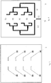
- fig. 4 a view of a lower dielectric layer with a first power network, second power network, a power line and a switching unit
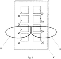
- fig. 5 shows an embodiment of the invention in an axonometric view with radiation characteristics marked.
- a microstrip antenna comprises two joined dielectric layers, an upper dielectric layer 1 arranged over a lower dielectric layer 4, and therebetween a shield 3 with 8 (eight) rectangular slots 30 is arranged.
- slots 30 are etched in the shield 3, in another embodiment, slots 30 are milled in the shield 3.
- At the outer side 1 of the upper dielectric layer 2 there are 8 (eight) radiators 20 arranged in two arrays each with 4 (four) identical radiators 20, entirely included on the surface of the upper dielectric layer 2 and being of a shape of a planar figure, for example a rectangular shape.
- radiators 20 are metallized.
- a first power network 53 and a second power network 54 as well as power line 51 are positioned.
- a conductive, made of copper in an embodiment, power line 51 is connected to a switching unit 52, which in an embodiment is a microwave three-way switch.
- the switching unit 52 is connected to the first power network 53 and the second power network 54, which enables directing the microwave power to a selected line array and generating one of two characteristics 6.
- the power networks 53 and 54 split up into 8 (eight) power strips 55 and power the individual radiators 20 arranged in two arrays.
- the power strips 55 in an embodiment are of a rectangular shape and the short side of each of the power strips 55 is parallel to the long side of the corresponding slot 30, i.e.
- each one of the slots 30 corresponds to the symmetry centre of the corresponding power strips 55 and radiators 20.
- Each one of the slots 30 is positioned between the power strip 55 and the corresponding radiator 20 to ensure electromagnetic coupling between the first power network 53, the second power network 54, and the radiators 20.
- the upper dielectric layer 2 and the lower dielectric layer 4 are glued together to provide a glued layer thickness of 0.101 mm.
- radiators 20 are glued on the upper dielectric layer 2.
- radiators 20 are formed on the upper dielectric layer 2 as a result of etching process.
- radiators 20 are formed on the upper dielectric layer 2 as a result of milling process.
- slots 30 in the shield 3 are of identical shape. In one embodiment, slots 30 in the shield 3 are of a rectangular shape.
- first power network 53 and the second power network 54 and the power line 51 are glued to the lower dielectric layer 4.
- the first power network 53 and the second power network 54 as well as the power line 51 are formed on the lower dielectric layer 4 as a result of etching process.
- the upper dielectric layer 2 is made of a ceramic-Teflon® laminate.
- the lower dielectric layer 4 is made of an epoxy glass laminate.
- the width of the power line 51 is 1.77 mm or, in another embodiment, has another value corresponding to specific impedance of the line of 50 ⁇ , i.e. impedance of the power line (51) is 50 ⁇ .
- impedance of the power line (51) is 50 ⁇ .
- a microwave junction is connected or another microstrip line.
Landscapes
- Physics & Mathematics (AREA)
- Electromagnetism (AREA)
- Waveguide Aerials (AREA)
- Variable-Direction Aerials And Aerial Arrays (AREA)
Abstract
Description
- The object of the invention is a broadband microstrip antenna with a switchable beam for the band of 3400-3600 MHz, intended to be used in LTE, 4G and 5G cellular telecommunication systems, in particular for "small cells" of heterogenic network layer cells by cellular telecommunication users as well as in other mobile radio communication systems.
- There are known microstrip antennas with a radiator shaped as a rectangle, circle or triangle. The radiator may be powered by a power network that is positioned on the same layer as the radiator, on a bottom layer of the radiator or on some other layer arranged under the layer with the radiator. The radiator may be powered directly by a microstrip line, by an adaptor or by an electromagnetic coupling through an slot. Single-layer microstrip antennas powered by a line are characterized by a narrower operation band. Broadening of the band is possible by means of addition of additional layers and enlargement of the thickness of the structure. Providing several radiators of this kind enables forming of an array and increase in the directional gain. Switching of the beam is possible by orienting the radiators in different directions and selecting one of the radiators in the array. Other switching methods are based on introduction of a discrete phase shift on the radiators.
- From
US 2006202892 a switched beam of an antenna arrangement is known. The method of controlling the antenna arrangement as described therein enables using of the antennas in a predetermined sequence where suitable time division for each of the antennas is ensured. -
US 2002000941 discloses an antenna arrangement for radiotelephones where the antenna is movable. Additionally, when in one of its positions, connection of the radiotelephone to the antenna may be provided in one of two points by means of a press button. -
WO 12048818A1 -
JP H01146408 - Document
CN 104868233 discloses configurable antennas that are connected, by means of switches, to a signal input. The solution is intended for emission of a circularly polarized wave. - Document
KR 20060001210 - Arrays of microstrip antennas with a switched beam are positioned on objects of an arcuate profile such as for example a surface of a cylinder. This makes it impossible to use arrays of microstrip antennas with a switched beam on flat surfaces such as e.g. walls of buildings. An antenna according to the invention may be positioned on flat surfaces such as walls of buildings or bus stop windshields.
- The invention provides a microstrip antenna comprising two joined dielectric layers, an upper dielectric layer and a lower dielectric layer, and a shield with slots positioned therebetween. On the upper dielectric layer radiators are positioned that have a shape of a planar figure entirely contained on the surface of the upper dielectric layer, and on the lower dielectric layer a first power network and a second power network as well as a power line are arranged. The microstrip antenna is characterized in that the power line is connected to a switching unit and the switching unit is connected to the first power network and the second power network, that split up into power strips and power the individual radiators arranged in two arrays. The slots are arranged so that each one of the slots is positioned between a power strip and the corresponding radiator.
- Preferably, the switching unit is a three-way switch.
- Preferably, the radiators are of identical shape.
- Preferably, the radiators are of a rectangular shape.
- Preferably, the slots in the shield are of identical shape.
- Preferably, the slots in the shield are of a rectangular shape.
- Preferably, the symmetry centre of each one of the slots corresponds to the symmetry centre of the corresponding power strips and radiators.
- Preferably, the radiators are arranged in two arrays each with four radiators.
- Preferably, the radiators are positioned at the outer side of the upper dielectric layer.
- Preferably, the radiators are glued on the upper dielectric layer.
- Preferably, the radiators are formed on the upper dielectric layer as a result of etching process.
- Preferably, the radiators are formed on the upper dielectric layer as a result of milling process.
- Preferably, the first power network and the second power network as well as the power line are arranged on the outer side of the lower dielectric layer.
- Preferably, the first power network and the second power network as well as the power line are glued to the lower dielectric layer.
- Preferably, the first power network and the second power network as well as the power line are formed on the lower dielectric layer as a result of etching process.
- Preferably, the upper dielectric layer is made of a ceramic-Teflon® laminate.
- Preferably, the lower dielectric layer is made of an epoxy glass laminate.
- Preferably, impedance of the power line is 50 Ω.
- An antenna according to the invention is a two-layer radiation structure enabling signal broadband transmission within the band of 3.4-3.6 GHz. Positioning of a shield between the two layers provides an electric separation between the power line and the array of radiators. Positioning of e.g. eight radiators in two columns enables obtaining a broad characteristics in the azimuth plane and narrow characteristics in the elevation plane. The use of two branches of the power network makes it possible to switch between the two characteristics in the azimuth plane.
- Two linear arrays of microstrip antennas in the subject solution are positioned parallel to each other. Only one of the two linear arrays is activated. The inactive linear array is a passive director and causes a change in the radiation direction. Selection of the active linear array, and thus the direction of radiation, is effected by means of a switch provided at the lowest level of the power network.
- The proposed solution enables increasing of the productivity of the base station by means of selection of one of the two antenna arrays. As a result it is possible to direct an antenna beam towards an area with greater concentration of users.
- The conductive shield between the two layers alleviates mutual couplings between the power network and radiators.
- The subject-matter of the invention is shown in the drawing where
fig. 1 shows an antenna in a side view,fig. 2 : a view of an upper dielectric layer along with radiators,fig. 3 : a view of a conductive shield with slots,fig. 4 : a view of a lower dielectric layer with a first power network, second power network, a power line and a switching unit,fig. 5 : shows an embodiment of the invention in an axonometric view with radiation characteristics marked. - In an embodiment, a microstrip antenna comprises two joined dielectric layers, an upper
dielectric layer 1 arranged over a lowerdielectric layer 4, and therebetween ashield 3 with 8 (eight)rectangular slots 30 is arranged. In one embodiment,slots 30 are etched in theshield 3, in another embodiment,slots 30 are milled in theshield 3. At theouter side 1 of the upperdielectric layer 2 there are 8 (eight)radiators 20 arranged in two arrays each with 4 (four)identical radiators 20, entirely included on the surface of the upperdielectric layer 2 and being of a shape of a planar figure, for example a rectangular shape. In an embodiment,radiators 20 are metallized. At theouter side 5 of the lower dielectric layer 4 afirst power network 53 and asecond power network 54 as well aspower line 51 are positioned. A conductive, made of copper in an embodiment,power line 51 is connected to aswitching unit 52, which in an embodiment is a microwave three-way switch. Theswitching unit 52 is connected to thefirst power network 53 and thesecond power network 54, which enables directing the microwave power to a selected line array and generating one of twocharacteristics 6. Thepower networks power strips 55 and power theindividual radiators 20 arranged in two arrays. The power strips 55 in an embodiment are of a rectangular shape and the short side of each of the power strips 55 is parallel to the long side of thecorresponding slot 30, i.e. the symmetry centre of each one of theslots 30 corresponds to the symmetry centre of thecorresponding power strips 55 andradiators 20. Each one of theslots 30 is positioned between thepower strip 55 and the correspondingradiator 20 to ensure electromagnetic coupling between thefirst power network 53, thesecond power network 54, and theradiators 20. - In another embodiment the
upper dielectric layer 2 is made of a ceramic-Teflon® laminate of a dielectric permittivity εr =3.5 and thickness h1= 1.524 mm. - In a further embodiment, the
upper dielectric layer 2 and the lowerdielectric layer 4 are glued together to provide a glued layer thickness of 0.101 mm. Under theupper dielectric layer 2 the lowerdielectric layer 4 is positioned, the latter being of a thickness h2=1 mm and made of a laminate of an epoxy glass laminate - FR4 laminate of a loss angle δ equal to 0.02 and permittivity εr of 4.3. - In one embodiment,
radiators 20 are glued on theupper dielectric layer 2. - In another embodiment,
radiators 20 are formed on theupper dielectric layer 2 as a result of etching process. - In another embodiment,
radiators 20 are formed on theupper dielectric layer 2 as a result of milling process. - In a further embodiment,
radiators 20 are of a rectangular shape having dimensions L=20.5 mm and W=19.4 mm. - In a further embodiment,
slots 30 in theshield 3 are of identical shape. In one embodiment,slots 30 in theshield 3 are of a rectangular shape. - In a further embodiment, the
first power network 53 and thesecond power network 54 and thepower line 51 are glued to the lowerdielectric layer 4. - In another embodiment, the
first power network 53 and thesecond power network 54 as well as thepower line 51 are formed on the lowerdielectric layer 4 as a result of etching process. - In one embodiment, the
upper dielectric layer 2 is made of a ceramic-Teflon® laminate. - In a further embodiment, the lower
dielectric layer 4 is made of an epoxy glass laminate. - In a further embodiment, the width of the
power line 51 is 1.77 mm or, in another embodiment, has another value corresponding to specific impedance of the line of 50 Ω, i.e. impedance of the power line (51) is 50 Ω. To thepower line 51, at the edge of the antenna, a microwave junction is connected or another microstrip line. - Embodiments are described herein solely in a form of a non-limiting indications concerning the invention and they cannot limit in any way the scope of protection as defined in the claims.
Claims (15)
- A microstrip antenna comprising two joined dielectric layers, an upper dielectric layer (2) and a lower dielectric layer (4), and a shield (3) with slots (30) positioned therebetween, where on the upper dielectric layer (2) radiators (20) are positioned that have a shape of a planar figure entirely contained on the surface of the upper dielectric layer (2), while on the lower dielectric layer (4) a first power network (53) and a second power network (54) as well as a power line (51) are arranged, characterized in that the power line (51) is connected to a switching unit (52), and the switching unit (52) is connected to the first power network (53) and the second power network (54), that split up into power strips (55) and power the individual radiators (20) arranged in two arrays, where the slots (30) are arranged so that each one of the slots (30) is positioned between a power strip (55) and the corresponding radiator (20).
- Antenna according to claim 1, characterized in that the switching unit (52) is a three-way switch.
- Antenna according to claim 1, characterized in that radiators (20) are of identical and/or a rectangular shape.
- Antenna according to claim 1, characterized in that the slots (30) in the shield (3) are of identical and/or a rectangular shape.
- Antenna according to any of the above claims 1-4, characterized in that the symmetry centre of each one of the slots (30) corresponds to the symmetry centre of the corresponding power strips (55) and radiators (20).
- Antenna according to claim 1, characterized in that radiators (20) are arranged in two arrays each with four radiators (20).
- Antenna according to claim 1, characterized in that radiators (20) are positioned at the outer side (1) of the upper dielectric layer (2).
- Antenna according to claim 7, characterized in that radiators (20) are glued on the upper dielectric layer (2).
- Antenna according to claim 7, characterized in that radiators (20) are formed on the upper dielectric layer (2) as a result of etching and/or milling process.
- Antenna according to claim 1, characterized in that the first power network (53) and the second power network (54) and the power line (51) are arranged on the outer side (5) of the lower dielectric layer (4).
- Antenna according to claim 10, characterized in that the first power network (53) and the second power network (54) and the power line (51) are glued to the lower dielectric layer (4).
- Antenna according to claim 10, characterized in that the first power network (53) and the second power network (54) and the power line (51) are formed on the lower dielectric layer (4) as a result of etching process.
- Antenna according to claim 1, characterized in that the upper dielectric layer (2) is made of a ceramic-Teflon® laminate.
- Antenna according to claim 1, characterized in that the lower dielectric layer (4) is made of an epoxy glass laminate.
- Antenna according to claim 1, characterized in that impedance of the power line (51) is 50 Ω.
Applications Claiming Priority (1)
| Application Number | Priority Date | Filing Date | Title |
|---|---|---|---|
| PL423159A PL423159A1 (en) | 2017-10-13 | 2017-10-13 | Microstrip antenna |
Publications (1)
| Publication Number | Publication Date |
|---|---|
| EP3471206A1 true EP3471206A1 (en) | 2019-04-17 |
Family
ID=64049047
Family Applications (1)
| Application Number | Title | Priority Date | Filing Date |
|---|---|---|---|
| EP18460063.3A Withdrawn EP3471206A1 (en) | 2017-10-13 | 2018-10-11 | Microstrip antenna |
Country Status (2)
| Country | Link |
|---|---|
| EP (1) | EP3471206A1 (en) |
| PL (1) | PL423159A1 (en) |
Citations (1)
| Publication number | Priority date | Publication date | Assignee | Title |
|---|---|---|---|---|
| US20150349421A1 (en) * | 2014-05-30 | 2015-12-03 | King Fahd University Of Petroleum And Minerals | Millimeter (mm) wave switched beam antenna system |
Family Cites Families (3)
| Publication number | Priority date | Publication date | Assignee | Title |
|---|---|---|---|---|
| IT1284996B1 (en) * | 1996-09-30 | 1998-05-28 | Italtel Spa | MICROSTRIP ANTENNA WITH CONTROL OF THE DIRECTION OF THE AXIS OF MAXIMUM IRRADIATION |
| US7911388B2 (en) * | 2007-12-12 | 2011-03-22 | Broadcom Corporation | Method and system for configurable antenna in an integrated circuit package |
| PL230083B1 (en) * | 2016-02-23 | 2018-09-28 | Politechnika Warszawska | Method for shaping directional pattern in the aerial array with time modulation and the aerial array with time modulation |
-
2017
- 2017-10-13 PL PL423159A patent/PL423159A1/en unknown
-
2018
- 2018-10-11 EP EP18460063.3A patent/EP3471206A1/en not_active Withdrawn
Patent Citations (1)
| Publication number | Priority date | Publication date | Assignee | Title |
|---|---|---|---|---|
| US20150349421A1 (en) * | 2014-05-30 | 2015-12-03 | King Fahd University Of Petroleum And Minerals | Millimeter (mm) wave switched beam antenna system |
Non-Patent Citations (3)
| Title |
|---|
| ARIS M A ET AL: "Simulation of radiation pattern reconfigurable microstrip patch antenna using feeding delay line technique", 2016 IEEE ASIA-PACIFIC CONFERENCE ON APPLIED ELECTROMAGNETICS (APACE), IEEE, 11 December 2016 (2016-12-11), pages 305 - 309, XP033092066, DOI: 10.1109/APACE.2016.7916448 * |
| GRZEGORZ BOGDAN ET AL: "Time-Modulated Antenna Array With Lossless Switching Network", IEEE ANTENNAS AND WIRELESS PROPAGATION LETTERS, vol. 15, 1 January 2016 (2016-01-01), US, pages 1827 - 1830, XP055559418, ISSN: 1536-1225, DOI: 10.1109/LAWP.2016.2538463 * |
| MUHAMUD KAYAT S ET AL: "Truncated rhombic microstrip patch array antenna with frequency reconfigurability", APPLIED ELECTROMAGNETICS (APACE), 2012 IEEE ASIA-PACIFIC CONFERENCE ON, IEEE, 11 December 2012 (2012-12-11), pages 313 - 317, XP032327994, ISBN: 978-1-4673-3114-2, DOI: 10.1109/APACE.2012.6457683 * |
Also Published As
| Publication number | Publication date |
|---|---|
| PL423159A1 (en) | 2019-04-23 |
Similar Documents
| Publication | Publication Date | Title |
|---|---|---|
| US10749272B2 (en) | Dual-polarized millimeter-wave antenna system applicable to 5G communications and mobile terminal | |
| EP3289635B1 (en) | Antennas including an array of dual radiating elements and power dividers for wireless electronic devices | |
| EP3298657B1 (en) | Antenna element for signals with three polarizations | |
| US10044111B2 (en) | Wideband dual-polarized patch antenna | |
| Ojaroudiparchin et al. | Multi-layer 5G mobile phone antenna for multi-user MIMO communications | |
| US20140368405A1 (en) | Inverted F-Antennas at a Wireless Communication Node | |
| US11276923B2 (en) | Multi-band antenna arrangement | |
| EP3465823B1 (en) | C-fed antenna formed on multi-layer printed circuit board edge | |
| CN110148828B (en) | Antenna unit and electronic device | |
| CN114336020B (en) | A broadband circularly polarized antenna array based on asymmetric slotted rectangular patches | |
| Elhabbash et al. | Design of dual-band dual-polarized MIMO antenna for mm-wave 5G base stations with octagonal prism structure | |
| Syrytsin et al. | Circularly polarized planar helix phased antenna array for 5G mobile terminals | |
| US20150214624A1 (en) | Micro base station antenna | |
| EP3261179B1 (en) | Leaky wave antenna | |
| EP2830151B1 (en) | Method and system for multiple feed point antennas | |
| CN102832451A (en) | Wide-band miniaturized gain-controllable directional antenna and manufacturing method thereof | |
| US20170133763A1 (en) | Patch antenna | |
| CN218677564U (en) | Single-frequency band and dual-frequency band reconfigurable microstrip quasi-yagi antenna | |
| CN108682971B (en) | A Ku/Ka Band Frequency Reconfigurable Microstrip Array Antenna | |
| EP4118707B1 (en) | An antenna arrangement | |
| Li et al. | A WLAN dual-polarized beam-reconfigurable antenna | |
| US20100245207A1 (en) | Multi-sector radiating device with an omni-directional mode | |
| CN108682960B (en) | Multi-frequency array antenna and communication system | |
| Naqvi et al. | Tri-band antenna array with defected ground structure for mm-wave 5G applications | |
| Pedram et al. | Evolution and move toward fifth-generation antenna |
Legal Events
| Date | Code | Title | Description |
|---|---|---|---|
| PUAI | Public reference made under article 153(3) epc to a published international application that has entered the european phase |
Free format text: ORIGINAL CODE: 0009012 |
|
| STAA | Information on the status of an ep patent application or granted ep patent |
Free format text: STATUS: THE APPLICATION HAS BEEN PUBLISHED |
|
| AK | Designated contracting states |
Kind code of ref document: A1 Designated state(s): AL AT BE BG CH CY CZ DE DK EE ES FI FR GB GR HR HU IE IS IT LI LT LU LV MC MK MT NL NO PL PT RO RS SE SI SK SM TR |
|
| AX | Request for extension of the european patent |
Extension state: BA ME |
|
| STAA | Information on the status of an ep patent application or granted ep patent |
Free format text: STATUS: REQUEST FOR EXAMINATION WAS MADE |
|
| 17P | Request for examination filed |
Effective date: 20191015 |
|
| RBV | Designated contracting states (corrected) |
Designated state(s): AL AT BE BG CH CY CZ DE DK EE ES FI FR GB GR HR HU IE IS IT LI LT LU LV MC MK MT NL NO PL PT RO RS SE SI SK SM TR |
|
| STAA | Information on the status of an ep patent application or granted ep patent |
Free format text: STATUS: EXAMINATION IS IN PROGRESS |
|
| 17Q | First examination report despatched |
Effective date: 20210217 |
|
| STAA | Information on the status of an ep patent application or granted ep patent |
Free format text: STATUS: THE APPLICATION IS DEEMED TO BE WITHDRAWN |
|
| 18D | Application deemed to be withdrawn |
Effective date: 20210629 |