EP3471160A1 - Composition for producing organic semiconductor devices - Google Patents
Composition for producing organic semiconductor devices Download PDFInfo
- Publication number
- EP3471160A1 EP3471160A1 EP17810063.2A EP17810063A EP3471160A1 EP 3471160 A1 EP3471160 A1 EP 3471160A1 EP 17810063 A EP17810063 A EP 17810063A EP 3471160 A1 EP3471160 A1 EP 3471160A1
- Authority
- EP
- European Patent Office
- Prior art keywords
- group
- organic semiconductor
- formula
- compound represented
- composition
- Prior art date
- Legal status (The legal status is an assumption and is not a legal conclusion. Google has not performed a legal analysis and makes no representation as to the accuracy of the status listed.)
- Granted
Links
Classifications
-
- H—ELECTRICITY
- H10—SEMICONDUCTOR DEVICES; ELECTRIC SOLID-STATE DEVICES NOT OTHERWISE PROVIDED FOR
- H10K—ORGANIC ELECTRIC SOLID-STATE DEVICES
- H10K71/00—Manufacture or treatment specially adapted for the organic devices covered by this subclass
- H10K71/10—Deposition of organic active material
- H10K71/12—Deposition of organic active material using liquid deposition, e.g. spin coating
- H10K71/15—Deposition of organic active material using liquid deposition, e.g. spin coating characterised by the solvent used
-
- H—ELECTRICITY
- H10—SEMICONDUCTOR DEVICES; ELECTRIC SOLID-STATE DEVICES NOT OTHERWISE PROVIDED FOR
- H10K—ORGANIC ELECTRIC SOLID-STATE DEVICES
- H10K10/00—Organic devices specially adapted for rectifying, amplifying, oscillating or switching; Organic capacitors or resistors having potential barriers
-
- H—ELECTRICITY
- H10—SEMICONDUCTOR DEVICES; ELECTRIC SOLID-STATE DEVICES NOT OTHERWISE PROVIDED FOR
- H10K—ORGANIC ELECTRIC SOLID-STATE DEVICES
- H10K85/00—Organic materials used in the body or electrodes of devices covered by this subclass
- H10K85/60—Organic compounds having low molecular weight
- H10K85/649—Aromatic compounds comprising a hetero atom
- H10K85/657—Polycyclic condensed heteroaromatic hydrocarbons
- H10K85/6576—Polycyclic condensed heteroaromatic hydrocarbons comprising only sulfur in the heteroaromatic polycondensed ring system, e.g. benzothiophene
-
- H—ELECTRICITY
- H10—SEMICONDUCTOR DEVICES; ELECTRIC SOLID-STATE DEVICES NOT OTHERWISE PROVIDED FOR
- H10K—ORGANIC ELECTRIC SOLID-STATE DEVICES
- H10K10/00—Organic devices specially adapted for rectifying, amplifying, oscillating or switching; Organic capacitors or resistors having potential barriers
- H10K10/40—Organic transistors
-
- H—ELECTRICITY
- H10—SEMICONDUCTOR DEVICES; ELECTRIC SOLID-STATE DEVICES NOT OTHERWISE PROVIDED FOR
- H10K—ORGANIC ELECTRIC SOLID-STATE DEVICES
- H10K71/00—Manufacture or treatment specially adapted for the organic devices covered by this subclass
- H10K71/10—Deposition of organic active material
- H10K71/12—Deposition of organic active material using liquid deposition, e.g. spin coating
- H10K71/13—Deposition of organic active material using liquid deposition, e.g. spin coating using printing techniques, e.g. ink-jet printing or screen printing
Definitions
- the present invention relates to a composition that contains an annelated ⁇ -conjugated molecule, which is an organic semiconductor material, dissolved in a solvent and is used for manufacturing an organic semiconductor device by printing.
- Transistors which are important semiconductor devices included in displays and computers, are currently manufactured using inorganic semiconductor materials such as polysilicon and amorphous silicon.
- Manufacture of thin film transistors using inorganic semiconductor materials by plasma-enhanced chemical vapor deposition (PECVD) or sputtering has problems that the temperature in the manufacturing process is high, that the manufacturing equipment is expensive and therefore raises the costs, and that the properties of transistors tend to be uneven when large-area thin film transistors are formed.
- the temperature in the manufacturing process limits available substrates, and glass substrates have therefore been mainly used.
- glass substrates have high heat resistance but have low impact resistance and low flexibility and since it is difficult to reduce the weight of glass substrates, it has been difficult to form light and flexible transistors using glass substrates.
- organic semiconductor devices employing organic semiconductor materials have been studied and developed actively in recent years. This is because the use of organic semiconductor materials enables manufacture of organic semiconductor devices at low manufacturing process temperatures by a simple method such as application, enables use of plastic substrates having low heat resistance, and enables weight reduction, flexibilization, and cost reduction of electronic devices such as displays.
- Patent Literature 1 discloses an N-shaped annelated ⁇ -conjugated molecule as an organic semiconductor material with good carrier mobility. It is also disclosed that a substance such as o-dichlorobenzene and 1,2-dimethoxybenzene is used as a solvent to dissolve the organic semiconductor material.
- Patent Literature 1 International Publication No. WO 2014/136827
- compositions for manufacturing an organic semiconductor device employing an organic semiconductor material provide high carrier mobility while other compositions provide low carrier mobility, even with the same solvent.
- the present invention has an object to provide a composition for manufacturing an organic semiconductor device, the composition enabling formation of an organic semiconductor device that stably shows high carrier mobility.
- the present invention provides a composition for manufacturing an organic semiconductor device, containing 2,3-dihydrobenzofuran as a solvent and an organic semiconductor material below, wherein the water content of the solvent is 0.25 wt% or less.
- the organic semiconductor material at least one compound selected from the group consisting of a compound represented by formula (1-1), a compound represented by formula (1-2), a compound represented by formula (1-3), a compound represented by formula (1-4), a compound represented by formula (1-5), and a compound represented by formula (1-6): wherein X 1 and X 2 are the same or different and each represent an oxygen atom, a sulfur atom, or a selenium atom. m is 0 or 1. n 1 and n 2 are the same or different and each represent 0 or 1.
- R 1 and R 2 are the same or different and each represent a fluorine atom, a C 1-20 alkyl group, a C 6-13 aryl group, a pyridyl group, a furyl group, a thienyl group, or a thiazolyl group, wherein 1 or 2 or more hydrogen atoms contained in the alkyl group may be substituted by a fluorine atom, and wherein 1 or 2 or more hydrogen atoms contained in the aryl group, the pyridyl group, the furyl group, the thienyl group, or the thiazolyl group may be substituted by a fluorine atom or an alkyl group having 1 to 10 carbon atoms.
- the organic semiconductor material is preferably at least one compound selected from the group consisting of a compound represented by formula (1-7), a compound represented by formula (1-8), a compound represented by formula (1-9), and a compound represented by formula (1-10) : wherein R 3 and R 4 are the same or different and each represent a C 1-20 alkyl group, a C 6-13 aryl group, a pyridyl group, a furyl group, a thienyl group, or a thiazolyl group.)
- the content of the solvent in the composition for manufacturing an organic semiconductor device is preferably 99.999 wt% or less.
- the content of the organic semiconductor material in the composition for manufacturing an organic semiconductor device is preferably 0.005 parts by weight or more per 100 parts by weight of the solvent.
- the content of 2,3-dihydrobenzofuran in the solvent contained in the composition for manufacturing an organic semiconductor device is preferably 50 wt% or more.
- the content of the at least one compound selected from the group consisting of the compound represented by formula (1-1), the compound represented by formula (1-2), the compound represented by formula (1-3), the compound represented by formula (1-4), the compound represented by formula (1-5), and the compound represented by formula (1-6) in the organic semiconductor material contained in the composition for manufacturing an organic semiconductor device is preferably 50 wt% or more.
- the present invention relates to the followings.
- an organic semiconductor device that stably shows high carrier mobility can be formed.
- composition according to the present invention contains 2,3-dihydrobenzofuran as a solvent and an organic semiconductor material below, and the solvent has a water content of 0.25 wt% or less.
- compounds represented by formulas (1-1) to (1-6) may be collectively referred to as the "specific organic semiconductor material”.
- the organic semiconductor material at least one compound selected from the group consisting of a compound represented by formula (1-1), a compound represented by formula (1-2), a compound represented by formula (1-3), a compound represented by formula (1-4), a compound represented by formula (1-5), and a compound represented by formula (1-6).
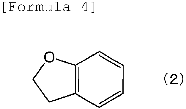
- 2,3-Dihydrobenzofuran is a compound represented by formula (2) below.
- the composition according to the present invention contains 2,3-dihydrobenzofuran as a solvent.
- 2,3-Dihydrobenzofuran dissolves the specific organic semiconductor material particularly well at high concentrations, has a drying property suitable for the temperatures in the process, and is apt to form the organic semiconductor material into a single crystal in a thin film.
- 2,3-dihydrobenzofuran in combination with the specific organic semiconductor material allows an organic semiconductor device formed by the composition according to the present invention to show high carrier mobility.
- the content of 2,3-dihydrobenzofuran in the total amount (100 wt%) of the solvent contained in the composition according to the present invention is preferably 50 wt% or more (such as 50 to 100 wt%), more preferably 80 wt% or more, further preferably 90 wt% or more, particularly preferably 95 wt% or more.
- the content is 50 wt% or more, the solubility of the specific organic semiconductor material is further improved, and the organic semiconductor material further tends to be formed into a single crystal in a thin film.
- composition according to the present invention may contain solvent(s) (other solvent(s)) other than 2,3-dihydrobenzofuran.
- solvent(s) other solvent(s)
- examples of the other solvent(s) above include solvents that are commonly used for electronic materials and are compatible with 2,3-dihydrobenzofuran.
- One or two or more types of the other solvents above may be contained.
- the water content of the solvent used for the composition according to the present invention is 0.25 wt% or less.
- a high water content of the composition according to the present invention tends to lower the carrier mobility, which is considered to be because crystallization of the specific organic semiconductor material is hindered and because the water is carrier-trapped.
- the water content of the composition according to the present invention containing 2,3-dihydrobenzofuran and the specific organic semiconductor material is 0.25 wt% or less, high carrier mobility is stably obtained.
- the water content is preferably 0.19 wt% or less, more preferably 0.08 wt% or less, further preferably 0.05 wt% or less.
- the water content of 2,3-dihydrobenzofuran preferably falls within the above range.
- the water content can be measured by the Karl Fischer method.
- composition according to the present invention contains at least one compound selected from the group consisting of the compound represented by formula (1-1), the compound represented by formula (1-2), the compound represented by formula (1-3), the compound represented by formula (1-4), the compound represented by formula (1-5), and the compound represented by formula (1-6) as the organic semiconductor material.
- the specific organic semiconductor material forms a herringbone structure of an organic semiconductor and has two-dimensional overlaps between ⁇ -electrons, thereby exhibiting high carrier mobility and high transistor properties as an organic semiconductor.
- X 1 and X 2 are the same or different and each represent an oxygen atom, a sulfur atom, or a selenium atom.
- an oxygen atom or a sulfur atom is preferable because high carrier mobility is obtained, and a sulfur atom is particularly preferable.
- m is 0 or 1, preferably 0 because good solubility in 2,3-dihydrobenzofuran and high carrier mobility are obtained.
- n 1 and n 2 are the same or different and each represent 0 or 1, preferably 1 because good solubility in 2,3-dihydrobenzofuran and high carrier mobility are obtained.
- R 1 and R 2 are the same or different and each represent a fluorine atom, a C 1-20 alkyl group, a C 6-13 aryl group, a pyridyl group, a furyl group, a thienyl group, or a thiazolyl group.
- Examples of the C 1-20 alkyl group for R 1 and R 2 include linear or branched alkyl groups such as a methyl group, an ethyl group, a propyl group, an isopropyl group, a n-butyl group, a t-butyl group, a n-pentyl group, a n-hexyl group, a n-heptyl group, a n-decyl group, a n-undecyl group, and a n-tetradecyl group.
- linear or branched alkyl groups such as a methyl group, an ethyl group, a propyl group, an isopropyl group, a n-butyl group, a t-butyl group, a n-pentyl group, a n-hexyl group, a n-heptyl group, a n-decyl group,
- a C 4-15 alkyl group is preferable, a C 6-12 alkyl group is more preferable, and a C 6-10 alkyl group is further preferable.
- One or two or more hydrogen atoms contained in the C 1-20 alkyl group may be substituted by a fluorine atom.
- Examples of the C 6-13 aryl group for R 1 and R 2 include phenyl, naphthyl, fluorenyl, and biphenylyl groups. Among these groups, a phenyl group is preferable.
- Examples of the pyridyl group include 2-pyridyl, 3-pyridyl, and 4-pyridyl groups.
- Examples of the furyl group include 2-furyl and 3-furyl groups.
- Examples of the thienyl group include 2-thienyl and 3-thienyl groups.
- Examples of the thiazolyl group include a 2-thiazolyl group.
- One or two or more hydrogen atoms contained in the aryl group, the pyridyl group, the furyl group, the thienyl group, and the thiazolyl group may be substituted by a fluorine atom or an alkyl group having 1 to 10 carbon atoms.
- alkyl group having 1 to 10 carbon atoms examples include linear or branched alkyl groups such as a methyl group, an ethyl group, a propyl group, an isopropyl group, a n-butyl group, a t-butyl group, a n-pentyl group, a n-hexyl group, a n-heptyl group, and a n-decyl group.
- an alkyl group having 1 to 6 carbon atoms is preferable, and an alkyl group having 1 to 3 carbon atoms is particularly preferable.
- Examples of a group in which at least one hydrogen atom contained in the aryl group is substituted by an alkyl group having 1 to 10 carbon atoms include a tolyl group and a xylyl group.
- Examples of a group in which at least one hydrogen atom contained in the aryl group is substituted by a fluorine atom include a p-fluorophenyl group and a pentafluorophenyl group.
- R 1 and R 2 are preferably the same or different and each represent a C 1-20 alkyl group, a C 6-13 aryl group, a pyridyl group, a furyl group, a thienyl group, or a thiazolyl group, more preferably a C 1-20 alkyl group, because solubility in 2,3-dihydrobenzofuran and high carrier mobility are obtained.
- the compound represented by formula (1-1), the compound represented by formula (1-4) and the compound represented by formula (1-6) are particularly preferable because their crystalline states can be maintained even at high temperatures higher than 120°C and because thin-film crystals with good thermal stability can be easily obtained.
- a compound represented by formula (1-7), a compound represented by formula (1-8), a compound represented by formula (1-9), and a compound represented by formula (1-10) are particularly preferable.
- R 3 and R 4 are the same or different and each represent a C 1-20 alkyl group, a C 6-13 aryl group, a pyridyl group, a furyl group, a thienyl group, or a thiazolyl group. Examples thereof include the above examples of the C 1-20 alkyl group, the C 6-13 aryl group, the pyridyl group, the furyl group, the thienyl group, and the thiazolyl group for R 1 and R 2 .
- R 3 and R 4 preferably represent the same group because solubility in 2,3-dihydrobenzofuran and high carrier mobility are obtained, more preferably each represent a C 1-20 alkyl group, a phenyl group, a furyl group, or a thienyl group, further preferably each represent a C 1-20 alkyl group (among these groups, a C 4-15 alkyl group is preferable, a C 6-12 alkyl group is more preferable, and a C 6-10 alkyl group is further preferable).
- the compound represented by formula (1-1) and the compound represented by formula (1-2) can be manufactured by, for example, the method disclosed in International Publication No. WO 2014/136827 .
- commercially available products bearing the trade names "C 10 -DNBDT-NW”, “C 6 -DNBDT-NW”, “Cs-DNBDT”, and “C6-DNT-VW” (manufactured by PI-CRYSTAL, INC.), the trade name "C 10 -DNTT” (manufactured by Daicel Corporation), and the trade name "C 8 -BTBT” (manufactured by Sigma-Aldrich Co. LLC) can be used as the specific organic semiconductor material.
- the specific organic semiconductor material has a molecular structure in which benzene rings range on both sides of at least one bending point, which is a crosslink formed by a chalcogen atom, and in which substituents have been introduced into the benzene rings at both ends.
- their solubility in 2,3-dihydrobenzofuran is higher than the solubility of a linear molecule having about the same number of rings, and the precipitation is less likely to occur even at low temperatures.
- the composition according to the present invention may contain an organic semiconductor material other than the above specific organic semiconductor material.
- an organic semiconductor material other than the above specific organic semiconductor material.
- the content of the above specific organic semiconductor material in the total amount (100 wt%) of organic semiconductor materials contained in the composition according to the present invention, but 50 wt% or more (such as 50 to 100 wt%) is preferable, 80 wt% or more is more preferable, 90 wt% or more is further preferable, and 95 wt% or more is particularly preferable.
- the content is the total content of the two or more specific organic semiconductor materials.
- composition for manufacturing an organic semiconductor device contains 2,3-dihydrobenzofuran as a solvent and at least one compound selected from among the compound represented by formula (1-1), the compound represented by formula (1-2), the compound represented by formula (1-3), the compound represented by formula (1-4), the compound represented by formula (1-5), and the compound represented by formula (1-6) as the organic semiconductor material.
- the combination of 2,3-dihydrobenzofuran and the specific organic semiconductor material in the composition according to the present invention enables easy production of a thin-film single crystal having a herringbone structure in the planar direction of the substrate after applying and drying the composition according to the present invention, and a crystal structure that exhibits high carrier mobility and is suitable for providing high transistor properties of an organic semiconductor is obtained.
- the water content of the solvent is 0.25 wt% or less.
- the composition according to the present invention provides more stable and high carrier mobility than in the case where the water content is more than 0.25 wt%.
- One organic semiconductor material may be used singly, or two or more organic semiconductor materials may be used in combination.
- the content of the solvent in the total amount (100 wt%) of the composition according to the present invention is, for example, 99.999 wt% or less. Its lower limit is, for example, 90.000 wt%, preferably 93.000 wt%, particularly preferably 95.000 wt%, and its upper limit is preferably 98.990 wt%. In particular, the content of 2,3-dihydrobenzofuran preferably falls within the above range.
- the content of the organic semiconductor material in the composition according to the present invention is, for example, 0.005 parts by weight or more, preferably 0.008 parts by weight or more, more preferably 0.01 parts by weight or more, based on 100 parts by weight of the solvent.
- the upper limit of the content of the organic semiconductor material is, for example, 1 part by weight, preferably 0.5 parts by weight, more preferably 0.2 parts by weight.
- the content of the specific organic semiconductor material preferably falls within the above range.
- compositions for manufacturing an organic semiconductor device may be blended into the composition according to the present invention as needed.
- components such as epoxy resins, acrylic resins, cellulose resins, and butyral resins commonly contained in compositions for manufacturing an organic semiconductor device may be blended into the composition according to the present invention as needed.
- an organic semiconductor device can be directly formed on a plastic substrate, which has lower heat resistance than the heat resistance of a glass substrate but is impact resistant, lightweight, and flexible, so that an impact resistant, lightweight, flexible display or computer can be formed.
- the specific organic semiconductor material contained in the composition crystallizes by self-organization, so that an organic semiconductor device with a high carrier mobility (such as 0.0005 cm 2 /Vs or more, preferably 0.001 cm 2 /Vs or more, more preferably 0.05 cm 2 /Vs or more, further preferably 0.1 cm 2 /Vs or more, particularly preferably 1.0 cm 2 /Vs or more) is obtained.
- the composition according to the present invention can dissolve the specific organic semiconductor material at a high concentration, the specific organic semiconductor material can be dissolved at a high concentration even at relatively low temperatures (such as 20 to 100°C, preferably 20 to 80°C).
- an organic electroluminescent element can be directly formed on a plastic substrate, which has lower heat resistance than the heat resistance of a glass substrate but is impact resistant, lightweight, and flexible, so that an impact resistant, lightweight, flexible display or computer can be formed.
- the composition according to the present invention contains 2,3-dihydrobenzofuran as a solvent, when the composition is applied over a substrate, the specific organic semiconductor material crystallizes by self-organization, so that a thin film of an organic semiconductor crystal (such as an organic electroluminescent element) with high crystallinity is obtained.
- the thin film of an organic semiconductor crystal can be easily formed by simple application such as printing and spin coating, so that the costs can be greatly reduced.
- composition according to the present invention can be prepared by, for example, mixing 2,3-dihydrobenzofuran and the specific organic semiconductor material and heating the mixture in an air, nitrogen, or argon atmosphere at a temperature of about 70 to 150°C for about 0.1 to 5 hours.
- C 10 -DNTT as an organic semiconductor material was mixed with 2,3-dihydrobenzofuran with a water content of 0.04 wt% as a solvent under an environment of 25°C such that the concentration of the organic semiconductor material was 0.03 wt%, and the mixture was heated in a nitrogen atmosphere in a shaded environment at 100°C for 3 hours, so that a composition (1) for manufacturing an organic semiconductor device was obtained. Dissolution of the organic semiconductor material in the resulting composition (1) for manufacturing an organic semiconductor device was confirmed by visual observation.
- a silicon substrate (SiO 2 , 100 ⁇ m in thickness) was washed with acetone and isopropanol using ultrasonic waves and was subjected to a UV ozone treatment at room temperature for 30 minutes.
- ⁇ -Phenethyltrichlorosilane was allowed to form a self-assembled monolayer at 120°C for 30 minutes to coat the substrate. Washing with toluene and isopropanol using ultrasonic waves was then performed.
- the composition (1) for manufacturing an organic semiconductor device was applied over the silicon substrate by edge casting disclosed in International Publication No. WO 2013/125599 .
- the product was dried in a vacuum at 100°C for 10 hours, and gold (40 nm) was deposited by vacuum evaporation on the product to form source and drain electrodes.
- a bottom-gate top-contact organic field-effect transistor (with a channel length of 100 ⁇ m and a channel width of 2 mm) was thus produced.
- the carrier mobility of the resulting element was measured using a semiconductor parameter analyzer (model number: "keithley 4200", manufactured by Keithley Instruments, Inc.).
- compositions for manufacturing an organic semiconductor device were prepared in substantially the same manner as in Example 1 except that organic semiconductor materials shown in Table 1 were used and that the contents of the solvent and the organic semiconductor materials are changed as shown in Table 1, organic field-effect transistors were produced, and their carrier mobilities were evaluated.
- compositions for manufacturing an organic semiconductor device were prepared in substantially the same manner as in Example 1 except that organic semiconductor materials shown in Table 1 were used, that 2,3-dihydrobenzofuran with water contents shown in Table 1 were used as the solvent, and that the contents of the solvent and the organic semiconductor materials were changed as shown in Table 1, organic field-effect transistors were produced, and their carrier mobilities were evaluated.
- DHBF 2,3-Dihydrobenzofuran, manufactured by Daicel Corporation
- composition according to the present invention can be used for manufacturing an organic semiconductor device by printing.
Landscapes
- Engineering & Computer Science (AREA)
- Physics & Mathematics (AREA)
- Spectroscopy & Molecular Physics (AREA)
- Chemical & Material Sciences (AREA)
- Materials Engineering (AREA)
- Manufacturing & Machinery (AREA)
- Thin Film Transistor (AREA)
- Heterocyclic Carbon Compounds Containing A Hetero Ring Having Oxygen Or Sulfur (AREA)
Abstract


Description
- The present invention relates to a composition that contains an annelated π-conjugated molecule, which is an organic semiconductor material, dissolved in a solvent and is used for manufacturing an organic semiconductor device by printing.
- Transistors, which are important semiconductor devices included in displays and computers, are currently manufactured using inorganic semiconductor materials such as polysilicon and amorphous silicon. Manufacture of thin film transistors using inorganic semiconductor materials by plasma-enhanced chemical vapor deposition (PECVD) or sputtering has problems that the temperature in the manufacturing process is high, that the manufacturing equipment is expensive and therefore raises the costs, and that the properties of transistors tend to be uneven when large-area thin film transistors are formed. In addition, the temperature in the manufacturing process limits available substrates, and glass substrates have therefore been mainly used. However, since glass substrates have high heat resistance but have low impact resistance and low flexibility and since it is difficult to reduce the weight of glass substrates, it has been difficult to form light and flexible transistors using glass substrates.
- Accordingly, organic semiconductor devices employing organic semiconductor materials have been studied and developed actively in recent years. This is because the use of organic semiconductor materials enables manufacture of organic semiconductor devices at low manufacturing process temperatures by a simple method such as application, enables use of plastic substrates having low heat resistance, and enables weight reduction, flexibilization, and cost reduction of electronic devices such as displays.
- Patent Literature 1 discloses an N-shaped annelated π-conjugated molecule as an organic semiconductor material with good carrier mobility. It is also disclosed that a substance such as o-dichlorobenzene and 1,2-dimethoxybenzene is used as a solvent to dissolve the organic semiconductor material.
- Patent Literature 1: International Publication No.
WO 2014/136827 - By the way, some compositions for manufacturing an organic semiconductor device employing an organic semiconductor material provide high carrier mobility while other compositions provide low carrier mobility, even with the same solvent.
- Hence, the present invention has an object to provide a composition for manufacturing an organic semiconductor device, the composition enabling formation of an organic semiconductor device that stably shows high carrier mobility.
- After earnest studies to solve the above problem, the present inventors have found that using a specific solvent with a water content of not more than a specific value and a specific organic semiconductor material achieves formation of an organic semiconductor device that stably shows high carrier mobility. The present invention has been completed on the basis of these findings.
- That is, the present invention provides a composition for manufacturing an organic semiconductor device, containing 2,3-dihydrobenzofuran as a solvent and an organic semiconductor material below, wherein the water content of the solvent is 0.25 wt% or less.
- The organic semiconductor material: at least one compound selected from the group consisting of a compound represented by formula (1-1), a compound represented by formula (1-2), a compound represented by formula (1-3), a compound represented by formula (1-4), a compound represented by formula (1-5), and a compound represented by formula (1-6):


- The organic semiconductor material is preferably at least one compound selected from the group consisting of a compound represented by formula (1-7), a compound represented by formula (1-8), a compound represented by formula (1-9), and a compound represented by formula (1-10) :

- The content of the solvent in the composition for manufacturing an organic semiconductor device is preferably 99.999 wt% or less.
- The content of the organic semiconductor material in the composition for manufacturing an organic semiconductor device is preferably 0.005 parts by weight or more per 100 parts by weight of the solvent.
- The content of 2,3-dihydrobenzofuran in the solvent contained in the composition for manufacturing an organic semiconductor device is preferably 50 wt% or more.
- The content of the at least one compound selected from the group consisting of the compound represented by formula (1-1), the compound represented by formula (1-2), the compound represented by formula (1-3), the compound represented by formula (1-4), the compound represented by formula (1-5), and the compound represented by formula (1-6) in the organic semiconductor material contained in the composition for manufacturing an organic semiconductor device is preferably 50 wt% or more.
- That is, the present invention relates to the followings.
- [1] A composition for manufacturing an organic semiconductor device, comprising 2,3-dihydrobenzofuran as a solvent and a semiconductor material, wherein the water content of the solvent is 0.25 wt% or less, and
the organic semiconductor material comprises at least one compound selected from the group consisting of a compound represented by formula (1-1), a compound represented by formula (1-2), a compound represented by formula (1-3), a compound represented by formula (1-4), a compound represented by formula (1-5), and a compound represented by formula (1-6):

- [2] The composition for manufacturing an organic semiconductor device according to [1], wherein the organic semiconductor material is at least one compound selected from the group consisting of the compound represented by formula (1-1), the compound represented by formula (1-4), and the compound represented by formula (1-6) .
- [3] The composition for manufacturing an organic semiconductor device according to [1] or [2], wherein X1 and X2 are the same or different and each represent an oxygen atom or a sulfur atom.
- [4] The composition for manufacturing an organic semiconductor device according to any one of [1] to [3], wherein m is 0.
- [5] The composition for manufacturing an organic semiconductor device according to any one of [1] to [4], wherein n1 and n2 each represent 1.
- [6] The composition for manufacturing an organic semiconductor device according to any one of [1] to [5], wherein R1 and R2 are the same or different and each represent a C1-20 alkyl group (preferably a C4-15 alkyl group, more preferably a C6-12 alkyl group, further preferably a C6-10 alkyl group), a C6-13 aryl group (preferably a phenyl group), a pyridyl group, a furyl group, a thienyl group, or a thiazolyl group (note that one or more hydrogen atom contained in the alkyl group may be substituted by a fluorine atom and that one or more hydrogen atom contained in the aryl group, the pyridyl group, the furyl group, the thienyl group, and the thiazolyl group may be substituted by a fluorine atom or an alkyl group having 1 to 10 carbon atoms).
- [7] The composition for manufacturing an organic semiconductor device according to any one of [1] to [5], wherein R1 and R2 are the same or different and each represent a C1-20 alkyl group (preferably a C4-15 alkyl group, more preferably a C6-12 alkyl group, further preferably a C6-10 alkyl group) (note that one or more hydrogen atom contained in the alkyl group may be substituted by a fluorine atom).
- [8] The composition for manufacturing an organic semiconductor device according to [1], wherein the organic semiconductor material is at least one compound selected from the group consisting of a compound represented by formula (1-7), a compound represented by formula (1-8), a compound represented by formula (1-9), and a compound represented by formula (1-10):


- [9] The composition for manufacturing an organic semiconductor device according to [8], wherein R3 and R4 are the same or different and each represent a C1-20 alkyl group (preferably a C4-15 alkyl group, more preferably a C6-12 alkyl group, further preferably a C6-10 alkyl group), a phenyl group, a furyl group, or a thienyl group.
- [10] The composition for manufacturing an organic semiconductor device according to [8], wherein R3 and R4 are the same or different and each represent a C1-20 alkyl group (preferably a C4-15 alkyl group, more preferably a C6-12 alkyl group, further preferably a C6-10 alkyl group).
- [11] The composition for manufacturing an organic semiconductor device according to any one of [8] to [10], wherein the content of the at least one compound selected from the group consisting of the compound represented by formula (1-7), the compound represented by formula (1-8), the compound represented by formula (1-9), and the compound represented by formula (1-10) in the organic semiconductor material contained in the composition for manufacturing an organic semiconductor device is 50 wt% or more (preferably 80 wt% or more, more preferably 90 wt% or more, further preferably 95 wt% or more).
- [12] The composition for manufacturing an organic semiconductor device according to any one of [1] to [11], wherein the content of the solvent (preferably 2,3-dihydrobenzofuran) in the composition for manufacturing an organic semiconductor device is 99.999 wt% or less.
- [13] The composition for manufacturing an organic semiconductor device according to any one of [1] to [12], wherein the content of the solvent (preferably 2,3-dihydrobenzofuran) in the composition for manufacturing an organic semiconductor device is 90.000 wt% or more (preferably 93.000 wt% or more, more preferably 95.000 wt% or more, further preferably 98.990 wt% or more).
- [14] The composition for manufacturing an organic semiconductor device according to any one of [1] to [13], wherein the content of the organic semiconductor material (preferably the at least one compound selected from the group consisting of the compound represented by formula (1-1), the compound represented by formula (1-2), the compound represented by formula (1-3), the compound represented by formula (1-4), the compound represented by formula (1-5), and the compound represented by formula (1-6)) in the composition for manufacturing an organic semiconductor device is 0.005 parts by weight or more (preferably 0.008 parts by weight or more, more preferably 0.01 parts by weight or more) based on 100 parts by weight of the solvent.
- [15] The composition for manufacturing an organic semiconductor device according to any one of [1] to [14], wherein the content of the organic semiconductor material (preferably the at least one compound selected from the group consisting of the compound represented by formula (1-1), the compound represented by formula (1-2), the compound represented by formula (1-3), the compound represented by formula (1-4), the compound represented by formula (1-5), and the compound represented by formula (1-6)) in the composition for manufacturing an organic semiconductor device is 1 part by weight or less (preferably 0.5 parts by weight or less, more preferably 0.2 parts by weight or less) based on 100 parts by weight of the solvent.
- [16] The composition for manufacturing an organic semiconductor device according to any one of [1] to [15], wherein the content of 2,3-dihydrobenzofuran in the solvent contained in the composition for manufacturing an organic semiconductor device is 50 wt% or more (preferably 80 wt% or more, more preferably 90 wt% or more, further preferably 95 wt% or more).
- [17] The composition for manufacturing an organic semiconductor device according to any one of [1] to [16], wherein the content of the at least one compound selected from the group consisting of the compound represented by formula (1-1), the compound represented by formula (1-2), the compound represented by formula (1-3), the compound represented by formula (1-4), the compound represented by formula (1-5), and the compound represented by formula (1-6) in the organic semiconductor material contained in the composition for manufacturing an organic semiconductor device is 50 wt% or more (preferably 80 wt% or more, more preferably 90 wt% or more, further preferably 95 wt% or more).
- [18] The composition for manufacturing an organic semiconductor device according to [17], wherein the content of at least one compound selected from the group consisting of the compound represented by formula (1-1), the compound represented by formula (1-4), and the compound represented by formula (1-6) in the organic semiconductor material contained in the composition for manufacturing an organic semiconductor device is 50 wt% or more (preferably 80 wt% or more, more preferably 90 wt% or more, further preferably 95 wt% or more).
- [19] The composition for manufacturing an organic semiconductor device according to any one of [1] to [18], wherein the water content of the solvent is 0.19 wt% or less (preferably 0.08 wt% or less, more preferably 0.05 wt% or less).
- [20] The composition for manufacturing an organic semiconductor device according to any one of [1] to [19], the composition being capable of forming an organic semiconductor device showing a carrier mobility of 0.0005 cm2/Vs or more (preferably 0.001 cm2/Vs or more, more preferably 0.05 cm2/Vs or more, further preferably 0.1 cm2/Vs or more, particularly preferably 1.0 cm2/Vs or more) .
- With the composition for manufacturing an organic semiconductor device according to the present invention, an organic semiconductor device that stably shows high carrier mobility can be formed.
- A composition for manufacturing an organic semiconductor device according to the present invention (which may be simply referred to as a "composition according to the present invention") contains 2,3-dihydrobenzofuran as a solvent and an organic semiconductor material below, and the solvent has a water content of 0.25 wt% or less. In this specification, compounds represented by formulas (1-1) to (1-6) may be collectively referred to as the "specific organic semiconductor material".
- The organic semiconductor material: at least one compound selected from the group consisting of a compound represented by formula (1-1), a compound represented by formula (1-2), a compound represented by formula (1-3), a compound represented by formula (1-4), a compound represented by formula (1-5), and a compound represented by formula (1-6).


- 2,3-Dihydrobenzofuran is a compound represented by formula (2) below. The composition according to the present invention contains 2,3-dihydrobenzofuran as a solvent. 2,3-Dihydrobenzofuran dissolves the specific organic semiconductor material particularly well at high concentrations, has a drying property suitable for the temperatures in the process, and is apt to form the organic semiconductor material into a single crystal in a thin film. Using 2,3-dihydrobenzofuran in combination with the specific organic semiconductor material allows an organic semiconductor device formed by the composition according to the present invention to show high carrier mobility.
- There is no particular limitation on the content of 2,3-dihydrobenzofuran in the total amount (100 wt%) of the solvent contained in the composition according to the present invention, but the content is preferably 50 wt% or more (such as 50 to 100 wt%), more preferably 80 wt% or more, further preferably 90 wt% or more, particularly preferably 95 wt% or more. When the content is 50 wt% or more, the solubility of the specific organic semiconductor material is further improved, and the organic semiconductor material further tends to be formed into a single crystal in a thin film.
- The composition according to the present invention may contain solvent(s) (other solvent(s)) other than 2,3-dihydrobenzofuran. Examples of the other solvent(s) above include solvents that are commonly used for electronic materials and are compatible with 2,3-dihydrobenzofuran. One or two or more types of the other solvents above may be contained.
- As described above, the water content of the solvent used for the composition according to the present invention is 0.25 wt% or less. A high water content of the composition according to the present invention tends to lower the carrier mobility, which is considered to be because crystallization of the specific organic semiconductor material is hindered and because the water is carrier-trapped. If the water content of the composition according to the present invention containing 2,3-dihydrobenzofuran and the specific organic semiconductor material is 0.25 wt% or less, high carrier mobility is stably obtained. The water content is preferably 0.19 wt% or less, more preferably 0.08 wt% or less, further preferably 0.05 wt% or less. The water content of 2,3-dihydrobenzofuran preferably falls within the above range. The water content can be measured by the Karl Fischer method.
- The composition according to the present invention contains at least one compound selected from the group consisting of the compound represented by formula (1-1), the compound represented by formula (1-2), the compound represented by formula (1-3), the compound represented by formula (1-4), the compound represented by formula (1-5), and the compound represented by formula (1-6) as the organic semiconductor material. The specific organic semiconductor material forms a herringbone structure of an organic semiconductor and has two-dimensional overlaps between π-electrons, thereby exhibiting high carrier mobility and high transistor properties as an organic semiconductor.
- In formulas (1-1) to (1-6), X1 and X2 are the same or different and each represent an oxygen atom, a sulfur atom, or a selenium atom. Among these atoms, an oxygen atom or a sulfur atom is preferable because high carrier mobility is obtained, and a sulfur atom is particularly preferable.
- m is 0 or 1, preferably 0 because good solubility in 2,3-dihydrobenzofuran and high carrier mobility are obtained.
- n1 and n2 are the same or different and each represent 0 or 1, preferably 1 because good solubility in 2,3-dihydrobenzofuran and high carrier mobility are obtained.
- R1 and R2 are the same or different and each represent a fluorine atom, a C1-20 alkyl group, a C6-13 aryl group, a pyridyl group, a furyl group, a thienyl group, or a thiazolyl group.
- Examples of the C1-20 alkyl group for R1 and R2 include linear or branched alkyl groups such as a methyl group, an ethyl group, a propyl group, an isopropyl group, a n-butyl group, a t-butyl group, a n-pentyl group, a n-hexyl group, a n-heptyl group, a n-decyl group, a n-undecyl group, and a n-tetradecyl group. Among these groups, a C4-15 alkyl group is preferable, a C6-12 alkyl group is more preferable, and a C6-10 alkyl group is further preferable. One or two or more hydrogen atoms contained in the C1-20 alkyl group may be substituted by a fluorine atom.
- Examples of the C6-13 aryl group for R1 and R2 include phenyl, naphthyl, fluorenyl, and biphenylyl groups. Among these groups, a phenyl group is preferable.
- Examples of the pyridyl group include 2-pyridyl, 3-pyridyl, and 4-pyridyl groups.
- Examples of the furyl group include 2-furyl and 3-furyl groups.
- Examples of the thienyl group include 2-thienyl and 3-thienyl groups.
- Examples of the thiazolyl group include a 2-thiazolyl group.
- One or two or more hydrogen atoms contained in the aryl group, the pyridyl group, the furyl group, the thienyl group, and the thiazolyl group may be substituted by a fluorine atom or an alkyl group having 1 to 10 carbon atoms. Examples of the alkyl group having 1 to 10 carbon atoms include linear or branched alkyl groups such as a methyl group, an ethyl group, a propyl group, an isopropyl group, a n-butyl group, a t-butyl group, a n-pentyl group, a n-hexyl group, a n-heptyl group, and a n-decyl group. Among these groups, an alkyl group having 1 to 6 carbon atoms is preferable, and an alkyl group having 1 to 3 carbon atoms is particularly preferable. Examples of a group in which at least one hydrogen atom contained in the aryl group is substituted by an alkyl group having 1 to 10 carbon atoms include a tolyl group and a xylyl group.
- Examples of a group in which at least one hydrogen atom contained in the aryl group is substituted by a fluorine atom include a p-fluorophenyl group and a pentafluorophenyl group.
- Among these groups, R1 and R2 are preferably the same or different and each represent a C1-20 alkyl group, a C6-13 aryl group, a pyridyl group, a furyl group, a thienyl group, or a thiazolyl group, more preferably a C1-20 alkyl group, because solubility in 2,3-dihydrobenzofuran and high carrier mobility are obtained.
- Among the above specific organic semiconductor materials, the compound represented by formula (1-1), the compound represented by formula (1-4) and the compound represented by formula (1-6) are particularly preferable because their crystalline states can be maintained even at high temperatures higher than 120°C and because thin-film crystals with good thermal stability can be easily obtained.
- As the specific organic semiconductor material, a compound represented by formula (1-7), a compound represented by formula (1-8), a compound represented by formula (1-9), and a compound represented by formula (1-10) are particularly preferable.


- In the above formulas, R3 and R4 are the same or different and each represent a C1-20 alkyl group, a C6-13 aryl group, a pyridyl group, a furyl group, a thienyl group, or a thiazolyl group. Examples thereof include the above examples of the C1-20 alkyl group, the C6-13 aryl group, the pyridyl group, the furyl group, the thienyl group, and the thiazolyl group for R1 and R2. Among these groups, R3 and R4 preferably represent the same group because solubility in 2,3-dihydrobenzofuran and high carrier mobility are obtained, more preferably each represent a C1-20 alkyl group, a phenyl group, a furyl group, or a thienyl group, further preferably each represent a C1-20 alkyl group (among these groups, a C4-15 alkyl group is preferable, a C6-12 alkyl group is more preferable, and a C6-10 alkyl group is further preferable).
- The compound represented by formula (1-1) and the compound represented by formula (1-2) can be manufactured by, for example, the method disclosed in International Publication No.
WO 2014/136827 . Alternatively, for example, commercially available products bearing the trade names "C10-DNBDT-NW", "C6-DNBDT-NW", "Cs-DNBDT", and "C6-DNT-VW" (manufactured by PI-CRYSTAL, INC.), the trade name "C10-DNTT" (manufactured by Daicel Corporation), and the trade name "C8-BTBT" (manufactured by Sigma-Aldrich Co. LLC) can be used as the specific organic semiconductor material. - The specific organic semiconductor material has a molecular structure in which benzene rings range on both sides of at least one bending point, which is a crosslink formed by a chalcogen atom, and in which substituents have been introduced into the benzene rings at both ends. Hence, their solubility in 2,3-dihydrobenzofuran is higher than the solubility of a linear molecule having about the same number of rings, and the precipitation is less likely to occur even at low temperatures.
- The composition according to the present invention may contain an organic semiconductor material other than the above specific organic semiconductor material. There is no particular limitation on the content of the above specific organic semiconductor material in the total amount (100 wt%) of organic semiconductor materials contained in the composition according to the present invention, but 50 wt% or more (such as 50 to 100 wt%) is preferable, 80 wt% or more is more preferable, 90 wt% or more is further preferable, and 95 wt% or more is particularly preferable. In the case where two or more of the specific organic semiconductor materials are contained, the content is the total content of the two or more specific organic semiconductor materials.
- The composition according to the present invention (composition for manufacturing an organic semiconductor device) contains 2,3-dihydrobenzofuran as a solvent and at least one compound selected from among the compound represented by formula (1-1), the compound represented by formula (1-2), the compound represented by formula (1-3), the compound represented by formula (1-4), the compound represented by formula (1-5), and the compound represented by formula (1-6) as the organic semiconductor material. The combination of 2,3-dihydrobenzofuran and the specific organic semiconductor material in the composition according to the present invention enables easy production of a thin-film single crystal having a herringbone structure in the planar direction of the substrate after applying and drying the composition according to the present invention, and a crystal structure that exhibits high carrier mobility and is suitable for providing high transistor properties of an organic semiconductor is obtained. The water content of the solvent is 0.25 wt% or less. With this constitution, the composition according to the present invention provides more stable and high carrier mobility than in the case where the water content is more than 0.25 wt%. One organic semiconductor material may be used singly, or two or more organic semiconductor materials may be used in combination.
- The content of the solvent in the total amount (100 wt%) of the composition according to the present invention is, for example, 99.999 wt% or less. Its lower limit is, for example, 90.000 wt%, preferably 93.000 wt%, particularly preferably 95.000 wt%, and its upper limit is preferably 98.990 wt%. In particular, the content of 2,3-dihydrobenzofuran preferably falls within the above range.
- There is no particular limitation on the content of the organic semiconductor material in the composition according to the present invention, but the content is, for example, 0.005 parts by weight or more, preferably 0.008 parts by weight or more, more preferably 0.01 parts by weight or more, based on 100 parts by weight of the solvent. The upper limit of the content of the organic semiconductor material is, for example, 1 part by weight, preferably 0.5 parts by weight, more preferably 0.2 parts by weight. In particular, the content of the specific organic semiconductor material preferably falls within the above range.
- In addition to the solvent and the organic semiconductor material, components (such as epoxy resins, acrylic resins, cellulose resins, and butyral resins) commonly contained in compositions for manufacturing an organic semiconductor device may be blended into the composition according to the present invention as needed.
- With the composition according to the present invention, an organic semiconductor device can be directly formed on a plastic substrate, which has lower heat resistance than the heat resistance of a glass substrate but is impact resistant, lightweight, and flexible, so that an impact resistant, lightweight, flexible display or computer can be formed. In addition, when the composition according to the present invention is applied over a substrate, the specific organic semiconductor material contained in the composition crystallizes by self-organization, so that an organic semiconductor device with a high carrier mobility (such as 0.0005 cm2/Vs or more, preferably 0.001 cm2/Vs or more, more preferably 0.05 cm2/Vs or more, further preferably 0.1 cm2/Vs or more, particularly preferably 1.0 cm2/Vs or more) is obtained.
- Since the composition according to the present invention can dissolve the specific organic semiconductor material at a high concentration, the specific organic semiconductor material can be dissolved at a high concentration even at relatively low temperatures (such as 20 to 100°C, preferably 20 to 80°C). Hence, an organic electroluminescent element can be directly formed on a plastic substrate, which has lower heat resistance than the heat resistance of a glass substrate but is impact resistant, lightweight, and flexible, so that an impact resistant, lightweight, flexible display or computer can be formed. In addition, since the composition according to the present invention contains 2,3-dihydrobenzofuran as a solvent, when the composition is applied over a substrate, the specific organic semiconductor material crystallizes by self-organization, so that a thin film of an organic semiconductor crystal (such as an organic electroluminescent element) with high crystallinity is obtained. In addition, the thin film of an organic semiconductor crystal can be easily formed by simple application such as printing and spin coating, so that the costs can be greatly reduced.
- The composition according to the present invention can be prepared by, for example, mixing 2,3-dihydrobenzofuran and the specific organic semiconductor material and heating the mixture in an air, nitrogen, or argon atmosphere at a temperature of about 70 to 150°C for about 0.1 to 5 hours.
- The following more specifically describes the present invention referring to Examples, but the Examples do not limit the present invention. The water content of 2,3-dihydrobenzofuran was measured with an apparatus bearing the trade name "Karl Fischer Titrator AQ-6 AQUA COUNTER" (manufactured by Hiranuma Sangyo Co., Ltd.).
- "C10-DNTT" as an organic semiconductor material was mixed with 2,3-dihydrobenzofuran with a water content of 0.04 wt% as a solvent under an environment of 25°C such that the concentration of the organic semiconductor material was 0.03 wt%, and the mixture was heated in a nitrogen atmosphere in a shaded environment at 100°C for 3 hours, so that a composition (1) for manufacturing an organic semiconductor device was obtained. Dissolution of the organic semiconductor material in the resulting composition (1) for manufacturing an organic semiconductor device was confirmed by visual observation.
- A silicon substrate (SiO2, 100 µm in thickness) was washed with acetone and isopropanol using ultrasonic waves and was subjected to a UV ozone treatment at room temperature for 30 minutes. β-Phenethyltrichlorosilane was allowed to form a self-assembled monolayer at 120°C for 30 minutes to coat the substrate. Washing with toluene and isopropanol using ultrasonic waves was then performed. The composition (1) for manufacturing an organic semiconductor device was applied over the silicon substrate by edge casting disclosed in International Publication No.
WO 2013/125599 . Subsequently, the product was dried in a vacuum at 100°C for 10 hours, and gold (40 nm) was deposited by vacuum evaporation on the product to form source and drain electrodes. A bottom-gate top-contact organic field-effect transistor (with a channel length of 100 µm and a channel width of 2 mm) was thus produced. The carrier mobility of the resulting element was measured using a semiconductor parameter analyzer (model number: "keithley 4200", manufactured by Keithley Instruments, Inc.). - Compositions for manufacturing an organic semiconductor device were prepared in substantially the same manner as in Example 1 except that organic semiconductor materials shown in Table 1 were used and that the contents of the solvent and the organic semiconductor materials are changed as shown in Table 1, organic field-effect transistors were produced, and their carrier mobilities were evaluated.
- Compositions for manufacturing an organic semiconductor device were prepared in substantially the same manner as in Example 1 except that organic semiconductor materials shown in Table 1 were used, that 2,3-dihydrobenzofuran with water contents shown in Table 1 were used as the solvent, and that the contents of the solvent and the organic semiconductor materials were changed as shown in Table 1, organic field-effect transistors were produced, and their carrier mobilities were evaluated.
-
(Table 1) Organic semiconductor material (wt%) DHBF (wt%) Carrier mobility (cm2/Vs) C10-CNTT Cs-DNBDT C6-DNT-VW C8-BTBT Water content 0.04 wt% Water content 0.19 wt% Water content 0.26 wt% Example 1 0.030 99.970 1.1 Example 2 0.015 99.985 5.0 Example 3 0.100 99.900 0.007 Example 4 0.100 99.900 0.02 Example 5 0.030 99.970 0.15 Example 6 0.015 99.985 4.5 Example 7 0.100 99.900 0.0006 Example 8 0.100 99.900 0.012 Comparative Example 1 0.030 99.970 0.09 Comparative Example 2 0.015 99.985 3.7 Comparative Example 3 0.100 99.900 0.000001 Comparative Example 4 0.100 99.900 0.0028 -
- C10-DNTT: The compound represented by formula (1-11) below bearing the trade name "C10-DNTT", manufactured by Daicel Corporation

- C8-DNBDT: The compound represented by formula (1-12) below bearing the trade name "C8-DNBDT", manufactured by PI-CRYSTAL, INC.


- C6-DNT-VW: The compound represented by formula (1-13) below bearing the trade name "C6-DNT-VW", manufactured by PI-CRYSTAL, INC.

- C8-BTBT: The compound represented by formula (1-14) below bearing the trade name "C8-BTBT", manufactured by Sigma-Aldrich Co. LLC

- DHBF: 2,3-Dihydrobenzofuran, manufactured by Daicel Corporation
- The composition according to the present invention can be used for manufacturing an organic semiconductor device by printing.
Claims (6)
- A composition for manufacturing an organic semiconductor device, comprising:2,3-dihydrobenzofuran as a solvent; andan organic semiconductor material,wherein a water content of the solvent is 0.25 wt% or less, andwherein the organic semiconductor material comprises at least one compound selected from the group consisting of a compound represented by formula (1-1), a compound represented by formula (1-2), a compound represented by formula (1-3), a compound represented by formula (1-4), a compound represented by formula (1-5), and a compound represented by formula (1-6):wherein X1 and X2 are the same or different and each represent an oxygen atom, a sulfur atom, or a selenium atom, m is 0 or 1, n1 and n2 are the same or different and each represent 0 or 1, and R1 and R2 are the same or different and each represent a fluorine atom, a C1-20 alkyl group, a C6-13 aryl group, a pyridyl group, a furyl group, a thienyl group, or a thiazolyl group, wherein 1 or 2 or more hydrogen atoms contained in the alkyl group may be substituted by a fluorine atom, and wherein 1 or 2 or more hydrogen atoms contained in the aryl group, the pyridyl group, the furyl group, the thienyl group, and the thiazolyl group may be substituted by a fluorine atom or an alkyl group having 1 to 10 carbon atoms).


- The composition for manufacturing an organic semiconductor device according to claim 1, wherein the organic semiconductor material comprises at least one compound selected from the group consisting of a compound represented by formula (1-7), a compound represented by formula (1-8), a compound represented by formula (1-9), and a compound represented by formula (1-10):

- The composition for manufacturing an organic semiconductor device according to claim 1 or 2, wherein a content of the solvent in the composition for manufacturing an organic semiconductor device is 99.999 wt% or less.
- The composition for manufacturing an organic semiconductor device according to any one of claims 1 to 3, wherein a content of the organic semiconductor material in the composition for manufacturing an organic semiconductor device is 0.005 parts by weight or more based on 100 parts by weight of the solvent.
- The composition for manufacturing an organic semiconductor device according to any one of claims 1 to 4, wherein a content of 2,3-dihydrobenzofuran in the solvent contained in the composition for manufacturing an organic semiconductor device is 50 wt% or more.
- The composition for manufacturing an organic semiconductor device according to any one of claims 1 to 5, wherein a content of the at least one compound selected from the group consisting of the compound represented by formula (1-1), the compound represented by formula (1-2), the compound represented by formula (1-3), the compound represented by formula (1-4), the compound represented by formula (1-5), and the compound represented by formula (1-6) in the organic semiconductor material contained in the composition for manufacturing an organic semiconductor device is 50 wt% or more.
Applications Claiming Priority (2)
| Application Number | Priority Date | Filing Date | Title |
|---|---|---|---|
| JP2016115659 | 2016-06-09 | ||
| PCT/JP2017/018473 WO2017212882A1 (en) | 2016-06-09 | 2017-05-17 | Composition for producing organic semiconductor devices |
Publications (3)
| Publication Number | Publication Date |
|---|---|
| EP3471160A1 true EP3471160A1 (en) | 2019-04-17 |
| EP3471160A4 EP3471160A4 (en) | 2020-02-26 |
| EP3471160B1 EP3471160B1 (en) | 2021-07-14 |
Family
ID=60578659
Family Applications (1)
| Application Number | Title | Priority Date | Filing Date |
|---|---|---|---|
| EP17810063.2A Active EP3471160B1 (en) | 2016-06-09 | 2017-05-17 | Composition for manufacturing organic semiconductor devices |
Country Status (7)
| Country | Link |
|---|---|
| US (1) | US10892424B2 (en) |
| EP (1) | EP3471160B1 (en) |
| JP (1) | JP6979402B2 (en) |
| KR (1) | KR102345789B1 (en) |
| CN (1) | CN109314186A (en) |
| TW (1) | TWI728123B (en) |
| WO (1) | WO2017212882A1 (en) |
Cited By (1)
| Publication number | Priority date | Publication date | Assignee | Title |
|---|---|---|---|---|
| EP3958335A4 (en) * | 2019-04-15 | 2023-02-01 | Daicel Corporation | Ink composition for producing organic semiconductor device |
Families Citing this family (1)
| Publication number | Priority date | Publication date | Assignee | Title |
|---|---|---|---|---|
| KR102191157B1 (en) * | 2018-03-06 | 2020-12-15 | 주식회사 엘지화학 | Multicyclic compound and organic light emitting device comprising the same |
Family Cites Families (15)
| Publication number | Priority date | Publication date | Assignee | Title |
|---|---|---|---|---|
| US6787063B2 (en) * | 2001-03-12 | 2004-09-07 | Seiko Epson Corporation | Compositions, methods for producing films, functional elements, methods for producing functional elements, methods for producing electro-optical devices and methods for producing electronic apparatus |
| JP4419373B2 (en) | 2001-10-10 | 2010-02-24 | セイコーエプソン株式会社 | Thin film forming method and electronic device forming method |
| KR20080100982A (en) * | 2007-05-15 | 2008-11-21 | 삼성전자주식회사 | Heteroacene compound, an organic thin film comprising the same and an electronic device comprising the thin film |
| JP5655301B2 (en) * | 2009-12-22 | 2015-01-21 | 東ソー株式会社 | Organic semiconductor materials |
| WO2012060460A1 (en) * | 2010-11-05 | 2012-05-10 | 住友化学株式会社 | Substituted chalcogeno-acene compound |
| JP5867583B2 (en) | 2012-02-22 | 2016-02-24 | Jnc株式会社 | Novel chalcogen-containing organic compounds and uses thereof |
| JP2014110347A (en) * | 2012-12-03 | 2014-06-12 | Tosoh Corp | Material for formation of organic semiconductor layer |
| CN104854719B (en) * | 2012-12-12 | 2018-11-13 | 株式会社大赛璐 | Organic transistor manufacture solvent or solvent compositions |
| JP6008158B2 (en) * | 2013-03-05 | 2016-10-19 | Jnc株式会社 | Chalcogen-containing organic compounds and uses thereof |
| DE112014005330T5 (en) * | 2013-11-21 | 2016-08-04 | Daicel Corporation | Solvent for producing an organic transistor |
| JP6302995B2 (en) * | 2014-03-03 | 2018-03-28 | 富士フイルム株式会社 | Organic transistor |
| JP6590361B2 (en) * | 2014-03-20 | 2019-10-16 | パイクリスタル株式会社 | Organic semiconductor film and manufacturing method thereof |
| JP6246150B2 (en) * | 2014-03-26 | 2017-12-13 | 富士フイルム株式会社 | Providing coating liquid for non-light-emitting organic semiconductor device, organic transistor, compound, organic semiconductor material for non-light-emitting organic semiconductor device, material for organic transistor, method for producing organic transistor, and method for producing organic semiconductor film |
| WO2016059972A1 (en) * | 2014-10-14 | 2016-04-21 | 東レ株式会社 | Organic semiconductor composition, photovoltaic element, photoelectric conversion device, and method for manufacturing photovoltaic element |
| KR20180098307A (en) * | 2015-12-22 | 2018-09-03 | 주식회사 다이셀 | Composition for the manufacture of organic semiconductor devices |
-
2017
- 2017-05-17 CN CN201780034357.3A patent/CN109314186A/en active Pending
- 2017-05-17 JP JP2018522392A patent/JP6979402B2/en not_active Expired - Fee Related
- 2017-05-17 US US16/308,352 patent/US10892424B2/en not_active Expired - Fee Related
- 2017-05-17 EP EP17810063.2A patent/EP3471160B1/en active Active
- 2017-05-17 KR KR1020187036161A patent/KR102345789B1/en not_active Expired - Fee Related
- 2017-05-17 WO PCT/JP2017/018473 patent/WO2017212882A1/en not_active Ceased
- 2017-06-08 TW TW106119002A patent/TWI728123B/en not_active IP Right Cessation
Cited By (1)
| Publication number | Priority date | Publication date | Assignee | Title |
|---|---|---|---|---|
| EP3958335A4 (en) * | 2019-04-15 | 2023-02-01 | Daicel Corporation | Ink composition for producing organic semiconductor device |
Also Published As
| Publication number | Publication date |
|---|---|
| EP3471160B1 (en) | 2021-07-14 |
| KR102345789B1 (en) | 2022-01-03 |
| CN109314186A (en) | 2019-02-05 |
| WO2017212882A1 (en) | 2017-12-14 |
| TWI728123B (en) | 2021-05-21 |
| EP3471160A4 (en) | 2020-02-26 |
| JPWO2017212882A1 (en) | 2019-04-04 |
| US10892424B2 (en) | 2021-01-12 |
| US20190214580A1 (en) | 2019-07-11 |
| TW201819389A (en) | 2018-06-01 |
| KR20190016964A (en) | 2019-02-19 |
| JP6979402B2 (en) | 2021-12-15 |
Similar Documents
| Publication | Publication Date | Title |
|---|---|---|
| JP5202545B2 (en) | Organic transistor using thiazolothiazole derivative and method for producing the same | |
| Jung et al. | Air‐operable, high‐mobility organic transistors with semifluorinated side chains and unsubstituted naphthalenetetracarboxylic diimide cores: high mobility and environmental and bias stress stability from the perfluorooctylpropyl side chain | |
| JP2010509789A5 (en) | ||
| Cranston et al. | High Performance Solution Processed n‐Type OTFTs through Surface Engineered F–F Interactions Using Asymmetric Silicon Phthalocyanines | |
| Fan et al. | Enhancing the thermal stability of organic field-effect transistors by electrostatically interlocked 2D molecular packing | |
| EP3471160B1 (en) | Composition for manufacturing organic semiconductor devices | |
| Minari et al. | Alkyl chain length dependent mobility of organic field-effect transistors based on thienyl-furan oligomers determined by the transfer line method | |
| JP2013534213A (en) | Semiconductors based on substituted [1] benzothieno [3,2-b] [1] -benzothiophene | |
| Caldera-Cruz et al. | Morphology, crystallinity, and electrical performance of solution-processed OFETs based on a DPP-based small molecule | |
| JP5335379B2 (en) | Organic semiconductor material and organic electronic device using the same | |
| EP3125321A1 (en) | Organic-semiconductor-film-forming composition | |
| Shi et al. | Organic semiconductors based on annelated β-oligothiophenes and its application for organic field-effect transistors | |
| KR101649553B1 (en) | Organic field-effect transistors, and method for preparing thereof | |
| JP6228129B2 (en) | Solvent or solvent composition for organic transistor production | |
| Tszydel et al. | Applications of parylene films in the manufacture of organic field-effect transistors | |
| WO2015076171A1 (en) | Solvent for producing organic transistor | |
| JP5948742B2 (en) | Composition for organic electronic device, method for producing organic electronic device, organic electronic device, and field effect transistor | |
| JP2008266312A (en) | Novel compounds and organic thin film transistors | |
| TWI775735B (en) | Composition for manufacturing organic semiconductor devices | |
| JP6643757B2 (en) | Organic field effect transistor | |
| Dull et al. | Broadening access to platelet-like crystal growth in organic semiconductors via solution processing | |
| Agina et al. | Organosilicon derivatives of BTBT for monolayer organic field effect transistors | |
| WO2024257469A1 (en) | Organic semiconductor composition, transistor manufacturing method, organic semiconductor thin film, and transistor | |
| Kashimura et al. | Transistor properties of novel organic conducting polymers bearing tetrathiafulvalene units in the backbone | |
| JP2003238490A (en) | Fullerene derivative and structure using the same |
Legal Events
| Date | Code | Title | Description |
|---|---|---|---|
| STAA | Information on the status of an ep patent application or granted ep patent |
Free format text: STATUS: THE INTERNATIONAL PUBLICATION HAS BEEN MADE |
|
| PUAI | Public reference made under article 153(3) epc to a published international application that has entered the european phase |
Free format text: ORIGINAL CODE: 0009012 |
|
| STAA | Information on the status of an ep patent application or granted ep patent |
Free format text: STATUS: REQUEST FOR EXAMINATION WAS MADE |
|
| 17P | Request for examination filed |
Effective date: 20190109 |
|
| AK | Designated contracting states |
Kind code of ref document: A1 Designated state(s): AL AT BE BG CH CY CZ DE DK EE ES FI FR GB GR HR HU IE IS IT LI LT LU LV MC MK MT NL NO PL PT RO RS SE SI SK SM TR |
|
| AX | Request for extension of the european patent |
Extension state: BA ME |
|
| DAV | Request for validation of the european patent (deleted) | ||
| DAX | Request for extension of the european patent (deleted) | ||
| A4 | Supplementary search report drawn up and despatched |
Effective date: 20200124 |
|
| RIC1 | Information provided on ipc code assigned before grant |
Ipc: H01L 51/00 20060101AFI20200120BHEP Ipc: H01L 51/30 20060101ALN20200120BHEP |
|
| REG | Reference to a national code |
Ref country code: DE Ref legal event code: R079 Ref document number: 602017042205 Country of ref document: DE Free format text: PREVIOUS MAIN CLASS: H01L0051300000 Ipc: H01L0051000000 |
|
| RIC1 | Information provided on ipc code assigned before grant |
Ipc: H01L 51/30 20060101ALN20210129BHEP Ipc: H01L 51/00 20060101AFI20210129BHEP |
|
| GRAP | Despatch of communication of intention to grant a patent |
Free format text: ORIGINAL CODE: EPIDOSNIGR1 |
|
| STAA | Information on the status of an ep patent application or granted ep patent |
Free format text: STATUS: GRANT OF PATENT IS INTENDED |
|
| RIC1 | Information provided on ipc code assigned before grant |
Ipc: H01L 51/00 20060101AFI20210301BHEP Ipc: H01L 51/30 20060101ALN20210301BHEP |
|
| INTG | Intention to grant announced |
Effective date: 20210322 |
|
| GRAS | Grant fee paid |
Free format text: ORIGINAL CODE: EPIDOSNIGR3 |
|
| GRAA | (expected) grant |
Free format text: ORIGINAL CODE: 0009210 |
|
| STAA | Information on the status of an ep patent application or granted ep patent |
Free format text: STATUS: THE PATENT HAS BEEN GRANTED |
|
| AK | Designated contracting states |
Kind code of ref document: B1 Designated state(s): AL AT BE BG CH CY CZ DE DK EE ES FI FR GB GR HR HU IE IS IT LI LT LU LV MC MK MT NL NO PL PT RO RS SE SI SK SM TR |
|
| REG | Reference to a national code |
Ref country code: GB Ref legal event code: FG4D |
|
| REG | Reference to a national code |
Ref country code: DE Ref legal event code: R096 Ref document number: 602017042205 Country of ref document: DE |
|
| REG | Reference to a national code |
Ref country code: IE Ref legal event code: FG4D |
|
| REG | Reference to a national code |
Ref country code: AT Ref legal event code: REF Ref document number: 1411342 Country of ref document: AT Kind code of ref document: T Effective date: 20210815 |
|
| REG | Reference to a national code |
Ref country code: LT Ref legal event code: MG9D |
|
| REG | Reference to a national code |
Ref country code: NL Ref legal event code: MP Effective date: 20210714 |
|
| REG | Reference to a national code |
Ref country code: AT Ref legal event code: MK05 Ref document number: 1411342 Country of ref document: AT Kind code of ref document: T Effective date: 20210714 |
|
| PG25 | Lapsed in a contracting state [announced via postgrant information from national office to epo] |
Ref country code: SE Free format text: LAPSE BECAUSE OF FAILURE TO SUBMIT A TRANSLATION OF THE DESCRIPTION OR TO PAY THE FEE WITHIN THE PRESCRIBED TIME-LIMIT Effective date: 20210714 Ref country code: RS Free format text: LAPSE BECAUSE OF FAILURE TO SUBMIT A TRANSLATION OF THE DESCRIPTION OR TO PAY THE FEE WITHIN THE PRESCRIBED TIME-LIMIT Effective date: 20210714 Ref country code: HR Free format text: LAPSE BECAUSE OF FAILURE TO SUBMIT A TRANSLATION OF THE DESCRIPTION OR TO PAY THE FEE WITHIN THE PRESCRIBED TIME-LIMIT Effective date: 20210714 Ref country code: FI Free format text: LAPSE BECAUSE OF FAILURE TO SUBMIT A TRANSLATION OF THE DESCRIPTION OR TO PAY THE FEE WITHIN THE PRESCRIBED TIME-LIMIT Effective date: 20210714 Ref country code: ES Free format text: LAPSE BECAUSE OF FAILURE TO SUBMIT A TRANSLATION OF THE DESCRIPTION OR TO PAY THE FEE WITHIN THE PRESCRIBED TIME-LIMIT Effective date: 20210714 Ref country code: NO Free format text: LAPSE BECAUSE OF FAILURE TO SUBMIT A TRANSLATION OF THE DESCRIPTION OR TO PAY THE FEE WITHIN THE PRESCRIBED TIME-LIMIT Effective date: 20211014 Ref country code: NL Free format text: LAPSE BECAUSE OF FAILURE TO SUBMIT A TRANSLATION OF THE DESCRIPTION OR TO PAY THE FEE WITHIN THE PRESCRIBED TIME-LIMIT Effective date: 20210714 Ref country code: PT Free format text: LAPSE BECAUSE OF FAILURE TO SUBMIT A TRANSLATION OF THE DESCRIPTION OR TO PAY THE FEE WITHIN THE PRESCRIBED TIME-LIMIT Effective date: 20211115 Ref country code: AT Free format text: LAPSE BECAUSE OF FAILURE TO SUBMIT A TRANSLATION OF THE DESCRIPTION OR TO PAY THE FEE WITHIN THE PRESCRIBED TIME-LIMIT Effective date: 20210714 Ref country code: BG Free format text: LAPSE BECAUSE OF FAILURE TO SUBMIT A TRANSLATION OF THE DESCRIPTION OR TO PAY THE FEE WITHIN THE PRESCRIBED TIME-LIMIT Effective date: 20211014 Ref country code: LT Free format text: LAPSE BECAUSE OF FAILURE TO SUBMIT A TRANSLATION OF THE DESCRIPTION OR TO PAY THE FEE WITHIN THE PRESCRIBED TIME-LIMIT Effective date: 20210714 |
|
| PG25 | Lapsed in a contracting state [announced via postgrant information from national office to epo] |
Ref country code: PL Free format text: LAPSE BECAUSE OF FAILURE TO SUBMIT A TRANSLATION OF THE DESCRIPTION OR TO PAY THE FEE WITHIN THE PRESCRIBED TIME-LIMIT Effective date: 20210714 Ref country code: LV Free format text: LAPSE BECAUSE OF FAILURE TO SUBMIT A TRANSLATION OF THE DESCRIPTION OR TO PAY THE FEE WITHIN THE PRESCRIBED TIME-LIMIT Effective date: 20210714 Ref country code: GR Free format text: LAPSE BECAUSE OF FAILURE TO SUBMIT A TRANSLATION OF THE DESCRIPTION OR TO PAY THE FEE WITHIN THE PRESCRIBED TIME-LIMIT Effective date: 20211015 |
|
| REG | Reference to a national code |
Ref country code: DE Ref legal event code: R097 Ref document number: 602017042205 Country of ref document: DE |
|
| PG25 | Lapsed in a contracting state [announced via postgrant information from national office to epo] |
Ref country code: DK Free format text: LAPSE BECAUSE OF FAILURE TO SUBMIT A TRANSLATION OF THE DESCRIPTION OR TO PAY THE FEE WITHIN THE PRESCRIBED TIME-LIMIT Effective date: 20210714 |
|
| PLBE | No opposition filed within time limit |
Free format text: ORIGINAL CODE: 0009261 |
|
| STAA | Information on the status of an ep patent application or granted ep patent |
Free format text: STATUS: NO OPPOSITION FILED WITHIN TIME LIMIT |
|
| PG25 | Lapsed in a contracting state [announced via postgrant information from national office to epo] |
Ref country code: SM Free format text: LAPSE BECAUSE OF FAILURE TO SUBMIT A TRANSLATION OF THE DESCRIPTION OR TO PAY THE FEE WITHIN THE PRESCRIBED TIME-LIMIT Effective date: 20210714 Ref country code: SK Free format text: LAPSE BECAUSE OF FAILURE TO SUBMIT A TRANSLATION OF THE DESCRIPTION OR TO PAY THE FEE WITHIN THE PRESCRIBED TIME-LIMIT Effective date: 20210714 Ref country code: RO Free format text: LAPSE BECAUSE OF FAILURE TO SUBMIT A TRANSLATION OF THE DESCRIPTION OR TO PAY THE FEE WITHIN THE PRESCRIBED TIME-LIMIT Effective date: 20210714 Ref country code: EE Free format text: LAPSE BECAUSE OF FAILURE TO SUBMIT A TRANSLATION OF THE DESCRIPTION OR TO PAY THE FEE WITHIN THE PRESCRIBED TIME-LIMIT Effective date: 20210714 Ref country code: CZ Free format text: LAPSE BECAUSE OF FAILURE TO SUBMIT A TRANSLATION OF THE DESCRIPTION OR TO PAY THE FEE WITHIN THE PRESCRIBED TIME-LIMIT Effective date: 20210714 Ref country code: AL Free format text: LAPSE BECAUSE OF FAILURE TO SUBMIT A TRANSLATION OF THE DESCRIPTION OR TO PAY THE FEE WITHIN THE PRESCRIBED TIME-LIMIT Effective date: 20210714 |
|
| 26N | No opposition filed |
Effective date: 20220419 |
|
| PG25 | Lapsed in a contracting state [announced via postgrant information from national office to epo] |
Ref country code: IT Free format text: LAPSE BECAUSE OF FAILURE TO SUBMIT A TRANSLATION OF THE DESCRIPTION OR TO PAY THE FEE WITHIN THE PRESCRIBED TIME-LIMIT Effective date: 20210714 |
|
| PGFP | Annual fee paid to national office [announced via postgrant information from national office to epo] |
Ref country code: GB Payment date: 20220520 Year of fee payment: 6 Ref country code: DE Payment date: 20220519 Year of fee payment: 6 |
|
| REG | Reference to a national code |
Ref country code: DE Ref legal event code: R079 Ref document number: 602017042205 Country of ref document: DE Free format text: PREVIOUS MAIN CLASS: H01L0051000000 Ipc: H10K0099000000 |
|
| REG | Reference to a national code |
Ref country code: CH Ref legal event code: PL |
|
| REG | Reference to a national code |
Ref country code: BE Ref legal event code: MM Effective date: 20220531 |
|
| PG25 | Lapsed in a contracting state [announced via postgrant information from national office to epo] |
Ref country code: MC Free format text: LAPSE BECAUSE OF FAILURE TO SUBMIT A TRANSLATION OF THE DESCRIPTION OR TO PAY THE FEE WITHIN THE PRESCRIBED TIME-LIMIT Effective date: 20210714 Ref country code: LU Free format text: LAPSE BECAUSE OF NON-PAYMENT OF DUE FEES Effective date: 20220517 Ref country code: LI Free format text: LAPSE BECAUSE OF NON-PAYMENT OF DUE FEES Effective date: 20220531 Ref country code: CH Free format text: LAPSE BECAUSE OF NON-PAYMENT OF DUE FEES Effective date: 20220531 |
|
| PG25 | Lapsed in a contracting state [announced via postgrant information from national office to epo] |
Ref country code: IE Free format text: LAPSE BECAUSE OF NON-PAYMENT OF DUE FEES Effective date: 20220517 Ref country code: FR Free format text: LAPSE BECAUSE OF NON-PAYMENT OF DUE FEES Effective date: 20220531 |
|
| PG25 | Lapsed in a contracting state [announced via postgrant information from national office to epo] |
Ref country code: BE Free format text: LAPSE BECAUSE OF NON-PAYMENT OF DUE FEES Effective date: 20220531 |
|
| REG | Reference to a national code |
Ref country code: DE Ref legal event code: R119 Ref document number: 602017042205 Country of ref document: DE |
|
| GBPC | Gb: european patent ceased through non-payment of renewal fee |
Effective date: 20230517 |
|
| PG25 | Lapsed in a contracting state [announced via postgrant information from national office to epo] |
Ref country code: HU Free format text: LAPSE BECAUSE OF FAILURE TO SUBMIT A TRANSLATION OF THE DESCRIPTION OR TO PAY THE FEE WITHIN THE PRESCRIBED TIME-LIMIT; INVALID AB INITIO Effective date: 20170517 |
|
| PG25 | Lapsed in a contracting state [announced via postgrant information from national office to epo] |
Ref country code: MK Free format text: LAPSE BECAUSE OF FAILURE TO SUBMIT A TRANSLATION OF THE DESCRIPTION OR TO PAY THE FEE WITHIN THE PRESCRIBED TIME-LIMIT Effective date: 20210714 Ref country code: DE Free format text: LAPSE BECAUSE OF NON-PAYMENT OF DUE FEES Effective date: 20231201 Ref country code: CY Free format text: LAPSE BECAUSE OF FAILURE TO SUBMIT A TRANSLATION OF THE DESCRIPTION OR TO PAY THE FEE WITHIN THE PRESCRIBED TIME-LIMIT Effective date: 20210714 Ref country code: GB Free format text: LAPSE BECAUSE OF NON-PAYMENT OF DUE FEES Effective date: 20230517 |
|
| PG25 | Lapsed in a contracting state [announced via postgrant information from national office to epo] |
Ref country code: TR Free format text: LAPSE BECAUSE OF FAILURE TO SUBMIT A TRANSLATION OF THE DESCRIPTION OR TO PAY THE FEE WITHIN THE PRESCRIBED TIME-LIMIT Effective date: 20210714 |
|
| PG25 | Lapsed in a contracting state [announced via postgrant information from national office to epo] |
Ref country code: MT Free format text: LAPSE BECAUSE OF FAILURE TO SUBMIT A TRANSLATION OF THE DESCRIPTION OR TO PAY THE FEE WITHIN THE PRESCRIBED TIME-LIMIT Effective date: 20210714 |