EP3471137A1 - Semiconductor device - Google Patents
Semiconductor device Download PDFInfo
- Publication number
- EP3471137A1 EP3471137A1 EP17813225.4A EP17813225A EP3471137A1 EP 3471137 A1 EP3471137 A1 EP 3471137A1 EP 17813225 A EP17813225 A EP 17813225A EP 3471137 A1 EP3471137 A1 EP 3471137A1
- Authority
- EP
- European Patent Office
- Prior art keywords
- bent portion
- skirt
- semiconductor device
- bent
- skirt portion
- Prior art date
- Legal status (The legal status is an assumption and is not a legal conclusion. Google has not performed a legal analysis and makes no representation as to the accuracy of the status listed.)
- Granted
Links
Images















Classifications
-
- H—ELECTRICITY
- H10—SEMICONDUCTOR DEVICES; ELECTRIC SOLID-STATE DEVICES NOT OTHERWISE PROVIDED FOR
- H10W—GENERIC PACKAGES, INTERCONNECTIONS, CONNECTORS OR OTHER CONSTRUCTIONAL DETAILS OF DEVICES COVERED BY CLASS H10
- H10W40/00—Arrangements for thermal protection or thermal control
- H10W40/10—Arrangements for heating
-
- H—ELECTRICITY
- H10—SEMICONDUCTOR DEVICES; ELECTRIC SOLID-STATE DEVICES NOT OTHERWISE PROVIDED FOR
- H10W—GENERIC PACKAGES, INTERCONNECTIONS, CONNECTORS OR OTHER CONSTRUCTIONAL DETAILS OF DEVICES COVERED BY CLASS H10
- H10W40/00—Arrangements for thermal protection or thermal control
- H10W40/20—Arrangements for cooling
- H10W40/25—Arrangements for cooling characterised by their materials
- H10W40/251—Organics
-
- H—ELECTRICITY
- H10—SEMICONDUCTOR DEVICES; ELECTRIC SOLID-STATE DEVICES NOT OTHERWISE PROVIDED FOR
- H10W—GENERIC PACKAGES, INTERCONNECTIONS, CONNECTORS OR OTHER CONSTRUCTIONAL DETAILS OF DEVICES COVERED BY CLASS H10
- H10W40/00—Arrangements for thermal protection or thermal control
- H10W40/20—Arrangements for cooling
- H10W40/25—Arrangements for cooling characterised by their materials
- H10W40/258—Metallic materials
-
- H—ELECTRICITY
- H10—SEMICONDUCTOR DEVICES; ELECTRIC SOLID-STATE DEVICES NOT OTHERWISE PROVIDED FOR
- H10W—GENERIC PACKAGES, INTERCONNECTIONS, CONNECTORS OR OTHER CONSTRUCTIONAL DETAILS OF DEVICES COVERED BY CLASS H10
- H10W40/00—Arrangements for thermal protection or thermal control
- H10W40/70—Fillings or auxiliary members in containers or in encapsulations for thermal protection or control
-
- H—ELECTRICITY
- H10—SEMICONDUCTOR DEVICES; ELECTRIC SOLID-STATE DEVICES NOT OTHERWISE PROVIDED FOR
- H10W—GENERIC PACKAGES, INTERCONNECTIONS, CONNECTORS OR OTHER CONSTRUCTIONAL DETAILS OF DEVICES COVERED BY CLASS H10
- H10W40/00—Arrangements for thermal protection or thermal control
- H10W40/70—Fillings or auxiliary members in containers or in encapsulations for thermal protection or control
- H10W40/77—Auxiliary members characterised by their shape
- H10W40/778—Auxiliary members characterised by their shape in encapsulations
-
- H—ELECTRICITY
- H10—SEMICONDUCTOR DEVICES; ELECTRIC SOLID-STATE DEVICES NOT OTHERWISE PROVIDED FOR
- H10W—GENERIC PACKAGES, INTERCONNECTIONS, CONNECTORS OR OTHER CONSTRUCTIONAL DETAILS OF DEVICES COVERED BY CLASS H10
- H10W74/00—Encapsulations, e.g. protective coatings
- H10W74/01—Manufacture or treatment
- H10W74/016—Manufacture or treatment using moulds
-
- H—ELECTRICITY
- H10—SEMICONDUCTOR DEVICES; ELECTRIC SOLID-STATE DEVICES NOT OTHERWISE PROVIDED FOR
- H10W—GENERIC PACKAGES, INTERCONNECTIONS, CONNECTORS OR OTHER CONSTRUCTIONAL DETAILS OF DEVICES COVERED BY CLASS H10
- H10W74/00—Encapsulations, e.g. protective coatings
- H10W74/10—Encapsulations, e.g. protective coatings characterised by their shape or disposition
-
- H—ELECTRICITY
- H10—SEMICONDUCTOR DEVICES; ELECTRIC SOLID-STATE DEVICES NOT OTHERWISE PROVIDED FOR
- H10W—GENERIC PACKAGES, INTERCONNECTIONS, CONNECTORS OR OTHER CONSTRUCTIONAL DETAILS OF DEVICES COVERED BY CLASS H10
- H10W74/00—Encapsulations, e.g. protective coatings
- H10W74/10—Encapsulations, e.g. protective coatings characterised by their shape or disposition
- H10W74/111—Encapsulations, e.g. protective coatings characterised by their shape or disposition the semiconductor body being completely enclosed
-
- H—ELECTRICITY
- H10—SEMICONDUCTOR DEVICES; ELECTRIC SOLID-STATE DEVICES NOT OTHERWISE PROVIDED FOR
- H10W—GENERIC PACKAGES, INTERCONNECTIONS, CONNECTORS OR OTHER CONSTRUCTIONAL DETAILS OF DEVICES COVERED BY CLASS H10
- H10W74/00—Encapsulations, e.g. protective coatings
- H10W74/10—Encapsulations, e.g. protective coatings characterised by their shape or disposition
- H10W74/111—Encapsulations, e.g. protective coatings characterised by their shape or disposition the semiconductor body being completely enclosed
- H10W74/121—Encapsulations, e.g. protective coatings characterised by their shape or disposition the semiconductor body being completely enclosed by multiple encapsulations, e.g. by a thin protective coating and a thick encapsulation
-
- H—ELECTRICITY
- H10—SEMICONDUCTOR DEVICES; ELECTRIC SOLID-STATE DEVICES NOT OTHERWISE PROVIDED FOR
- H10W—GENERIC PACKAGES, INTERCONNECTIONS, CONNECTORS OR OTHER CONSTRUCTIONAL DETAILS OF DEVICES COVERED BY CLASS H10
- H10W74/00—Encapsulations, e.g. protective coatings
- H10W74/10—Encapsulations, e.g. protective coatings characterised by their shape or disposition
- H10W74/111—Encapsulations, e.g. protective coatings characterised by their shape or disposition the semiconductor body being completely enclosed
- H10W74/127—Encapsulations, e.g. protective coatings characterised by their shape or disposition the semiconductor body being completely enclosed characterised by arrangements for sealing or adhesion
-
- H—ELECTRICITY
- H10—SEMICONDUCTOR DEVICES; ELECTRIC SOLID-STATE DEVICES NOT OTHERWISE PROVIDED FOR
- H10W—GENERIC PACKAGES, INTERCONNECTIONS, CONNECTORS OR OTHER CONSTRUCTIONAL DETAILS OF DEVICES COVERED BY CLASS H10
- H10W74/00—Encapsulations, e.g. protective coatings
- H10W74/40—Encapsulations, e.g. protective coatings characterised by their materials
-
- H—ELECTRICITY
- H10—SEMICONDUCTOR DEVICES; ELECTRIC SOLID-STATE DEVICES NOT OTHERWISE PROVIDED FOR
- H10W—GENERIC PACKAGES, INTERCONNECTIONS, CONNECTORS OR OTHER CONSTRUCTIONAL DETAILS OF DEVICES COVERED BY CLASS H10
- H10W72/00—Interconnections or connectors in packages
- H10W72/071—Connecting or disconnecting
- H10W72/076—Connecting or disconnecting of strap connectors
- H10W72/07631—Techniques
-
- H—ELECTRICITY
- H10—SEMICONDUCTOR DEVICES; ELECTRIC SOLID-STATE DEVICES NOT OTHERWISE PROVIDED FOR
- H10W—GENERIC PACKAGES, INTERCONNECTIONS, CONNECTORS OR OTHER CONSTRUCTIONAL DETAILS OF DEVICES COVERED BY CLASS H10
- H10W72/00—Interconnections or connectors in packages
- H10W72/071—Connecting or disconnecting
- H10W72/076—Connecting or disconnecting of strap connectors
- H10W72/07631—Techniques
- H10W72/07636—Soldering or alloying
-
- H—ELECTRICITY
- H10—SEMICONDUCTOR DEVICES; ELECTRIC SOLID-STATE DEVICES NOT OTHERWISE PROVIDED FOR
- H10W—GENERIC PACKAGES, INTERCONNECTIONS, CONNECTORS OR OTHER CONSTRUCTIONAL DETAILS OF DEVICES COVERED BY CLASS H10
- H10W72/00—Interconnections or connectors in packages
- H10W72/071—Connecting or disconnecting
- H10W72/076—Connecting or disconnecting of strap connectors
- H10W72/07651—Connecting or disconnecting of strap connectors characterised by changes in properties of the strap connectors during connecting
-
- H—ELECTRICITY
- H10—SEMICONDUCTOR DEVICES; ELECTRIC SOLID-STATE DEVICES NOT OTHERWISE PROVIDED FOR
- H10W—GENERIC PACKAGES, INTERCONNECTIONS, CONNECTORS OR OTHER CONSTRUCTIONAL DETAILS OF DEVICES COVERED BY CLASS H10
- H10W72/00—Interconnections or connectors in packages
- H10W72/60—Strap connectors, e.g. thick copper clips for grounding of power devices
-
- H—ELECTRICITY
- H10—SEMICONDUCTOR DEVICES; ELECTRIC SOLID-STATE DEVICES NOT OTHERWISE PROVIDED FOR
- H10W—GENERIC PACKAGES, INTERCONNECTIONS, CONNECTORS OR OTHER CONSTRUCTIONAL DETAILS OF DEVICES COVERED BY CLASS H10
- H10W72/00—Interconnections or connectors in packages
- H10W72/851—Dispositions of multiple connectors or interconnections
- H10W72/853—On the same surface
- H10W72/871—Bond wires and strap connectors
-
- H—ELECTRICITY
- H10—SEMICONDUCTOR DEVICES; ELECTRIC SOLID-STATE DEVICES NOT OTHERWISE PROVIDED FOR
- H10W—GENERIC PACKAGES, INTERCONNECTIONS, CONNECTORS OR OTHER CONSTRUCTIONAL DETAILS OF DEVICES COVERED BY CLASS H10
- H10W74/00—Encapsulations, e.g. protective coatings
Definitions
- the present invention relates to a semiconductor device of a resin-molded type.
- a semiconductor element such as an insulated gate bipolar transistor (IGBT), a metal-oxide-semiconductor field-effect transistor (MOSFET), an integrated circuit (IC) chip, or a large scale integrated circuit (LSI) chip is die-bonded to a lead frame for external terminal, and then electrically connected to a wire by a wire bond process or an inner lead such as a copper plate or a copper alloy by soldering, thereby allowing input and output of signals from and to the outside.
- IGBT insulated gate bipolar transistor
- MOSFET metal-oxide-semiconductor field-effect transistor
- IC integrated circuit
- LSI large scale integrated circuit
- a surface (mounting surface) of a lead frame on the side where a semiconductor element is mounted and a heat dissipation surface on the opposite side are sealed by an insulation resin using transfer molding.
- a semiconductor device for power a semiconductor element that generates a large amount of heat is provided inside, and therefore an insulation resin for sealing is required to have high thermal conductivity.
- a semiconductor device is proposed in which, in a molding resin sealing process, the heat dissipation surface side is sealed by a high heat dissipation conductive resin having a thermal conductivity of 3 W/m ⁇ K to 10 W/m ⁇ K, and the mounting surface side is sealed by a low-stress resin or the like.
- molding with two types of resins i.e., the resin for the mounting surface side and the resin for the heat dissipation surface side forms an interface between the two types of resins.
- An electric field is likely to concentrate on the interface, and the interface has poor adhesiveness, which causes peeling, leading to a problem that insulation property is deteriorated.
- a semiconductor device of Patent Document 1 includes: a plate-like lead frame having first and second main surfaces and a pattern shape and having an external terminal therearound; a semiconductor element fixed on the first main surface; a heatsink provided so as to be opposed to the second main surface with a gap therebetween; and sealing resin for sealing the semiconductor element, the lead frame, and the heatsink.
- the sealing resin includes a primary sealing resin and a secondary sealing resin having higher thermal conductivity than the primary sealing resin.
- the secondary sealing resin has: a part that is in close contact with the second main surface and fills the gap between the lead frame and the heatsink; and a protrusion integrally connected to the above part and penetrating a gap of the lead frame accompanying the pattern shape, to protrude in a wall shape toward the first main surface side.
- the primary sealing resin is in close contact with the first main surface and encloses the semiconductor element, and also is in close contact with the protrusion.
- Patent Document 1 Japanese Laid-Open Patent Publication JP 9-153 572 A .
- Patent Document 1 the creeping distance between parts of the lead frame that are adjacent to each other via a gap, along the interface between the primary sealing resin and the secondary sealing resin, is increased, whereby insulation performance of the parts of the lead frame is improved, leading to an effect of improving withstand voltage.
- the present invention has been made to solve the above problems, and an object of the present invention is to provide a semiconductor device that has a longer creeping distance between a lead frame and a heatsink than a conventional one and thus has improved insulation performance.
- a semiconductor device includes: a lead frame with a semiconductor element mounted thereto; a first insulation resin portion formed on a mounting surface side of the lead frame on which the semiconductor element is mounted; a second insulation resin portion formed on a heat dissipation surface side of the lead frame which is opposite to the mounting surface side; and a heatsink fixed to a heat dissipation surface of the second insulation resin portion, wherein the second insulation resin portion has a thin molded portion in close contact with the lead frame, and a second skirt portion formed at an end of the thin molded portion, the first insulation resin portion has a first skirt portion protruding toward the heat dissipation surface side of the lead frame and covering the second skirt portion of the second insulation resin portion, and an outer peripheral surface part of the second skirt portion has a first end connected to the lead frame and the first skirt portion, a second end connected to the heatsink, and at least one bent portion formed between the first end and the second end.
- the semiconductor device according to the present invention has a longer creeping distance from the lead frame to the heatsink than a conventional one and thus has improved insulation performance.
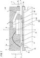
- FIG. 1 is a side sectional view showing the configuration of a semiconductor device according to the present Embodiment 1
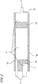
- FIG. 2 is a schematic plan view of the semiconductor device in which a first insulation resin portion is formed in a first-time transfer molding step, as seen from the heat dissipation surface side.
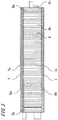
- FIG. 3 is a schematic plan view of the semiconductor device in which a second insulation resin portion is formed in a second-time transfer molding step, as seen from the heat dissipation surface side
- FIG. 4 is a sectional view along A-A line of the semiconductor device shown in FIG. 1
- FIG. 5 is an enlarged view of part B1 of the semiconductor device shown in FIG. 4 .
- a heatsink is not shown.
- the same or corresponding parts are denoted by the same reference characters.
- a semiconductor device 100 includes a semiconductor element 1, a lead frame 2, an external terminal 4, a wire 5, an inner lead 6, a first insulation resin portion 7, a second insulation resin portion 8, and a heatsink 50.
- the semiconductor element 1 such as IGBT, MOSFET, IC chip, or LSI chip is mounted above a surface (hereinafter, referred to as mounting surface 2a) of the lead frame 2 that is on the upper side in the drawing, with a joining member 3 such as solder or silver interposed therebetween.
- the lead frame 2 is made from a copper plate, a copper alloy plate, or the like, and the surface of the lead frame 2 is coated by metallic plating of gold, silver, nickel, tin, or the like (not shown).
- An electrode pad of the semiconductor element 1 is electrically connected to the external terminal 4 via the wire 5 connected by wire bonding, or via the inner lead 6 made from a material such as a copper plate or a copper alloy plate, and the semiconductor element 1 performs input and output of signals from and to an external device via the external terminal 4.
- the wire 5 is made from gold, silver, aluminum, copper, or the like, and the wire diameter thereof is about 20 ⁇ m to 500 ⁇ m.
- the inner lead 6 is joined to the semiconductor element 1 or the lead frame 2 via a joining member 3 such as solder or silver. It is noted that the wire 5 and the inner lead 6 are replaceable with each other.
- the first insulation resin portion 7 made from a first insulation resin is formed on the mounting surface 2a side of the lead frame 2.
- the second insulation resin portion 8 made from a second insulation resin is formed on the heat dissipation surface 2b side of the lead frame 2 which is opposite to the mounting surface 2a.
- a part 10 (hereinafter, referred to as die pad interval part 10) between two separate areas of the lead frame 2 is filled with the first insulation resin, to form the first insulation resin portion 7.
- the second insulation resin portion 8 has a thin molded portion 8b formed in contact with the heat dissipation surface 2b of the lead frame 2.
- the thickness of the thin molded portion 8b is about 0.02 mm to 0.3 mm.
- the heatsink 50 made of copper, aluminum, or the like is joined, via a heat dissipation member such as grease or by resin molding, to a heat dissipation surface 8b2 of the thin molded portion 8b which is opposite to a lead frame joining surface 8b1 in contact with the lead frame 2.
- the insulation resins forming the first insulation resin portion 7 and the second insulation resin portion 8 are both thermosetting epoxy resin or the like. It is noted that the second insulation resin portion 8 formed on the heat dissipation surface 2b side of the lead frame 2 is made of an insulation resin having higher thermal conductivity than the first insulation resin portion 7 formed on the mounting surface 2a side.
- the second insulation resin forming the second insulation resin portion 8 contains a filler such as silica, alumina, boron nitride, or aluminum nitride having high thermal conductivity, and the thermal conductivity of the second insulation resin portion 8 is 3 W/m ⁇ K to 12 W/m ⁇ K.
- a low-stress insulation resin having great fluidity which is used for a general semiconductor device, is used.
- a low-stress insulation resin obtained by adding silicone to a thermosetting epoxy resin or the like, or a low-stress insulation resin having a thermal expansion coefficient close to that of the lead frame is used.
- the second insulation resin portion 8 has the thin molded portion 8b having a thickness of about 0.02 mm to 0.3 mm and formed in close contact with the heat dissipation surface 2b of the lead frame 2, and the second skirt portion 8a having a first protrusion 81 protruding from an end of the thin molded portion 8b toward the heat dissipation surface 8b2 side of the second insulation resin portion 8.
- the first insulation resin portion 7 has the first skirt portion 7a protruding toward the heat dissipation surface 2b side of the lead frame 2 and covering the second skirt portion 8a.
- the first skirt portion 7a and the second skirt portion 8a have protrusion shapes such that the virtual-direction thicknesses thereof from the heat dissipation surface 2b of the lead frame 2 are about 0.3 mm to 2 mm which is thicker than the thickness of the thin molded portion 8b.
- the second skirt portion 8a has, at an outer peripheral surface part thereof: a first end T1 connected to the lead frame 2 and the first skirt portion 7a; a second end T2 connected to the heatsink 50; and at least one bent portion formed between the first end T1 and the second end T2, i.e., a first bent portion R1 formed at the first protrusion 81. Part from the first end T1 to the first bent portion R1 forms a first joining portion J1 between the first skirt portion 7a and the second skirt portion 8a.
- part from the first end T1 to the first bent portion R1 is shown in a straight shape
- part from the first bent portion R1 to the second end T2 is shown in a straight shape.
- These parts shown in straight shapes have flat plane shapes.
- the first skirt portion 7a and the second skirt portion 8a are molded with resin by transfer molding, and thus these plane shapes have irregularity to a certain degree.
- part between the first end and the bent portion, part between the bent portions, and part between the bent portion and the second end, which are shown in straight shapes have flat plane shapes as in the above case.
- the first bent portion R1 is shown in a rectangular shape.
- the second skirt portion 8a is molded with resin by transfer molding and thus has a curved part or irregularity to a certain degree.
- FIG. 6 is a sectional view of a semiconductor device in a comparative example of the present embodiment, along A-A line in FIG. 1 , and corresponds to FIG. 4 .
- FIG. 7 is an enlarged view of part B2 of the semiconductor device shown in FIG. 6 .
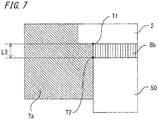
- the semiconductor device in the comparative example shown in FIG. 6 and FIG. 7 does not have the second skirt portion 8a protruding from an end of the thin molded portion 8b toward the heat dissipation surface side as in the present embodiment, and a creeping distance L from the lead frame 2 to the heatsink 50 is a distance L3 from the first end T1 connected to the lead frame 2, the first skirt portion 7a, and the thin molded portion 8b, to the second end T2 connected to the heatsink 50, the first skirt portion 7a, and the thin molded portion 8b.
- part from the first end T1 to the first bent portion R1 is the first joining portion J1 which is the interface between the first skirt portion 7a and the second skirt portion 8a.
- the creeping distance from the lead frame 2 to the heatsink 50 is greatly increased and insulation property is improved, as compared to the semiconductor device in the comparative example shown in FIG. 6 and FIG. 7 .
- the creeping distance from the lead frame to the heatsink extends in a straight line via the interface of the primary sealing resin and the secondary sealing resin, whereas the creeping distance in the present embodiment extends from the first end T1 of the lead frame 2 via the first bent portion R1 to the second end T2 of the heatsink 50. Therefore, the creeping distance is increased and insulation property is also improved.
- the outer peripheral surface part of the second skirt portion 8a is formed in a straight line extending from the first end T1 toward the heat dissipation side to reach the first bent portion R1.
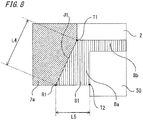
- the outer peripheral surface part of the second skirt portion 8a may be sloped outward from the first end T1 to the first bent portion R1.
- the second skirt portion 8a has a trapezoidal shape, and the creeping distance from the lead frame 2 to the heatsink 50 is the sum (L4 + L5) of a distance L4 from the first end T1 to the first bent portion R1 and a distance L5 from the first bent portion R1 to the second end T2, and thus is longer than the creeping distance (L1 + L2) in the semiconductor device shown in FIG. 4 and FIG. 5 .
- the outer peripheral surface part of the second skirt portion 8a may be formed in an arc shape expanding outward from the first end T1 to the first bent portion R1.
- the creeping distance from the lead frame 2 to the heatsink 50 is the sum of the distance from the first end T1 to the first bent portion R1 and the distance from the first bent portion R1 to the second end T2, and thus is longer than the creeping distance (L1 + L2) in the semiconductor device shown in FIG. 4 and FIG. 5 .
- a side surface portion 50A of the heatsink 50 may be separated from one side surface portion 8a1 of the second skirt portion 8a.
- the creeping distance from the lead frame 2 to the heatsink 50 is the sum of the distance from the first end T1 to the first bent portion R1, the distance from the first bent portion R1 to a bent portion R50, the distance from the bent portion R50 to a bent portion R51, and the distance from the bent portion R51 to the second end T2, and thus is longer than the creeping distance (L1 + L2) in the semiconductor device shown in FIG. 4 and FIG. 5 .
- FIG. 11 is a sectional view of a semiconductor device in Modification 4 of the present embodiment, along A-A line in FIG. 1 , and corresponds to FIG. 4 .
- FIG. 12 is an enlarged view of part B3 of the semiconductor device shown in FIG. 11 .
- the second skirt portion 8a has the first protrusion 81 protruding toward the heat dissipation surface 8b2 side of the thin molded portion 8b, and a second protrusion 82 protruding from the first protrusion 81 toward the side surface (X direction in the drawing) of the semiconductor device 100, and further has the first bent portion R1 formed at the first protrusion 81 and a second bent portion R2 formed at the second protrusion 82.
- the second skirt portion 8a is formed so as to cover the inner side surface and a surface that is on the lower side in the drawing, of the first skirt portion 7a.
- the creeping distance from the lead frame 2 to the heatsink 50 is the sum of the distance from the first end T1 to the first bent portion R1, the distance from the first bent portion R1 to the second bent portion R2, the distance from the second bent portion R2 to a bent portion R52, and the distance from the bent portion R52 to the second end T2, and thus is longer than the creeping distance (L1 + L2) in the semiconductor device shown in FIG. 4 and FIG. 5 .
- the heatsink 50 may be joined to the heat dissipation surface side of the second protrusion 82 of the second skirt portion 8a.
- the creeping distance from the lead frame 2 to the heatsink 50 is the sum of the distance from the first end T1 to the first bent portion R1, the distance from the first bent portion R1 to the second bent portion R2, and the distance from the second bent portion R2 to the second end T2, and thus is longer than the creeping distance (L1 + L2) in the semiconductor device shown in FIG. 4 and FIG. 5 .
- FIG. 14 is a sectional view of a semiconductor device in Modification 5 of the present embodiment, along A-A line in FIG. 1 , and corresponds to FIG. 4 .
- FIG. 15 is an enlarged view of part B4 of the semiconductor device shown in FIG. 14 .
- the second skirt portion 8a has the first protrusion 81 protruding toward the heat dissipation surface 8b2 side of the thin molded portion 8b, the second protrusion 82 protruding from the first protrusion 81 toward the side surface (X direction in the drawing) of the semiconductor device 100, and a third protrusion 83 protruding toward the mounting surface side of the lead frame 2 from the second protrusion 82, and further has the first bent portion R1 formed at the first protrusion 81, the second bent portion R2 formed at the second protrusion 82, and a third bent portion R3 formed at the third protrusion 83.
- Part from the first end T1 to the first bent portion R1 is the first joining portion J1 between the first skirt portion 7a and the second skirt portion 8a
- part from the first bent portion R1 to the second bent portion R2 is the second joining portion J2 between the first skirt portion 7a and the second skirt portion 8a
- part from the second bent portion R2 to the third bent portion R3 is a third joining portion J3 between the first skirt portion 7a and the second skirt portion 8a.
- the second skirt portion 8a is formed so as to cover the inner side surface, the outer side surface, and a surface that is on the lower side in the drawing, of the first skirt portion 7a.
- the creeping distance from the lead frame 2 to the heatsink 50 is the sum of the distance from the first end T1 to the first bent portion R1, the distance from the first bent portion R1 to the second bent portion R2, the distance from the second bent portion R2 to the third bent portion R3, the distance from the third bent portion R3 to a bent portion R53, the distance from the bent portion R53 to a bent portion R54, and the distance from the bent portion R54 to the second end T2, and thus is longer than the creeping distance (L1 + L2) in the semiconductor device shown in FIG. 4 and FIG. 5 .
- the heatsink 50 may be joined to the heat dissipation surface side of the second protrusion 82 of the second skirt portion 8a.
- the creeping distance from the lead frame 2 to the heatsink 50 is the sum of the distance from the first end T1 to the first bent portion R1, the distance from the first bent portion R1 to the second bent portion R2, the distance from the second bent portion R2 to the third bent portion R3, the distance from the third bent portion R3 to the bent portion R53, and the distance from the bent portion R53 to the second end T2, and thus is longer than the creeping distance (L1 + L2) in the semiconductor device shown in FIG. 4 and FIG. 5 .
- the semiconductor device includes: a lead frame with a semiconductor element mounted thereto; a first insulation resin portion formed on the mounting surface side of the lead frame on which the semiconductor element is mounted; a second insulation resin portion formed on the heat dissipation surface side of the lead frame which is opposite to the mounting surface side; and a heatsink fixed to the heat dissipation surface side of the second insulation resin portion.
- the second insulation resin portion has a thin molded portion in close contact with the lead frame, and a second skirt portion formed at an end of the thin molded portion.
- the first insulation resin portion has a first skirt portion protruding toward the heat dissipation surface side of the lead frame and covering the second skirt portion of the second insulation resin portion.
- the outer peripheral surface part of the second skirt portion has a first end connected to the lead frame and the first skirt portion, a second end connected to the heatsink, and at least one bent portion formed between the first end and the second end. Therefore, the creeping distance from the lead frame to the heatsink is increased as compared to a conventional one, whereby insulation performance is improved.
- the protrusion-direction thicknesses of the first skirt portion and the second skirt portion are greater than the thickness of the thin molded portion. Therefore, it is possible to increase the creeping distance between the lead frame and the heatsink by a necessary insulation distance, and prevent decrease in heat dissipation.
- first skirt portion and the second skirt portion are provided, the strength and the insulation distance at an outer peripheral end part of the lead frame to which voltage is applied can be ensured.
- the case where the surface of the lead frame is coated by metallic plating of gold, silver, nickel, tin, or the like has been described.
- the surface of the lead frame may not be coated.
- the lead frame has a uniform thickness.
- the lead frame may have a different thickness at some part thereof.
- the case of joining the heatsink to the thin molded portion via a heat dissipation member such as grease has been described.
- a heat dissipation member may not be used.
- the mounting surface side of the lead frame may also have the same heat dissipation property as the heat dissipation surface side.
- a high heat dissipation resin having a thermal conductivity of 3 W/m ⁇ K to 12 W/m ⁇ K, which is the same as the second insulation resin portion may be used as the first insulation resin portion. Since the periphery of the semiconductor element which is a heat generating component is sealed by the high heat dissipation resin, heat is dissipated from the entire periphery of the semiconductor element and thus heat dissipation is increased.
- the first skirt portion formed from the first insulation resin is located on the long side and the second skirt portion formed from the second insulation resin is located on the short side.
- this configuration may be reversed depending on the position of the gate of a molding die to be used.
- the positions of the sides formed by the first skirt portion molded with the first insulation resin and the second skirt portion molded with the second insulation resin are not limited to those shown in FIG. 3 , and also, the number of the sides of each of the first skirt portion and the second skirt portion is not limited to two.
- the position of a gate break left part 7b occurring after the first insulation resin portion is molded or the position of a gate break left part 8c occurring after the second insulation resin portion is molded is not limited to that shown in FIG. 1 and FIG. 3 , and also, the number thereof is not limited to one but may be plural.
- the second insulation resin portion is molded in the second-time transfer molding step.
- the first insulation resin portion may be molded in the second-time transfer molding step.
- FIG. 17 is a sectional view of the semiconductor device in the present Embodiment 2, along A-A line in FIG. 1 , and corresponds to FIG. 4 .
- FIG. 18 is an enlarged view of part B5 of the semiconductor device shown in FIG. 17 .
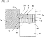
- the second skirt portion 8a has a step portion 800 extending in parallel with the lead frame 2 from an end of the thin molded portion 8b, and the first skirt portion 7a has a first wraparound portion 700 formed between the step portion 800 and the heat dissipation surface 2b of the lead frame 2.
- a fourth bent portion R4 and a fifth bent portion R5 are formed along a fourth joining portion J4 between the step portion 800 of the second skirt portion 8a and the first wraparound portion 700 of the first skirt portion 7a.
- the creeping distance from the lead frame 2 to the heatsink 50 is the sum of the distance from the first end T1 to the fourth bent portion R4, the distance from the fourth bent portion R4 to the fifth bent portion R5, and the distance from the fifth bent portion R5 to the second end T2, and thus is longer than the creeping distance (L1) in the semiconductor device shown in FIG. 6 and FIG. 7 . Therefore, insulation performance is improved.
- FIG. 19 is a sectional view of a semiconductor device in Modification 1 of Embodiment 2, along A-A line in FIG. 1 , and corresponds to FIG. 4 .
- FIG. 20 is an enlarged view of part B6 of the semiconductor device shown in FIG. 19 .
- the second skirt portion 8a has a fourth protrusion 84 protruding from the step portion 800 toward the heat dissipation surface side of the thin molded portion 8b, and a sixth bent portion R6 is formed at the fourth protrusion 84.
- Part from the fifth bent portion R5 to the sixth bent portion R6 is a fifth joining portion J5 between the first skirt portion 7a and the second skirt portion 8a.
- the creeping distance from the lead frame 2 to the heatsink 50 is the sum of the distance from the first end T1 to the fourth bent portion R4, the distance from the fourth bent portion R4 to the fifth bent portion R5, the distance from the fifth bent portion R5 to the sixth bent portion R6, and the distance from the sixth bent portion R6 to the second end T2, and thus is longer than the creeping distance L1 in the semiconductor device shown in FIG. 6 and FIG. 7 .
- the side surface portion 50A of the heatsink 50 may be separated from one side surface portion 8a1 of the second skirt portion 8a.
- the creeping distance from the lead frame 2 to the heatsink 50 is the sum of the distance from the first end T1 to the fourth bent portion R4, the distance from the fourth bent portion R4 to the fifth bent portion R5, the distance from the fifth bent portion R5 to the sixth bent portion R6, the distance from the sixth bent portion R6 to a bent portion R60, the distance from the bent portion R60 to a bent portion R61, and the distance from the bent portion R61 to the second end T2, and thus is longer than the creeping distance L1 in the semiconductor device shown in FIG. 6 and FIG. 7 .
- FIG. 22 is a sectional view of a semiconductor device in Modification 2 of Embodiment 2, along A-A line in FIG. 1 , and corresponds to FIG. 4 .
- FIG. 23 is an enlarged view of part B7 of the semiconductor device shown in FIG. 22 .
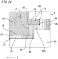
- the second skirt portion 8a has a fifth protrusion 85 protruding from the fourth protrusion 84 toward the side surface (X direction in the drawing) of the semiconductor device 100, and a seventh bent portion R7 is formed at the fifth protrusion 85.
- a sixth joining portion J6 Part from the sixth bent portion R6 to the seventh bent portion R7 is a sixth joining portion J6 between the first skirt portion 7a and the second skirt portion 8a.
- the creeping distance from the lead frame 2 to the heatsink 50 is the sum of the distance from the first end T1 to the fourth bent portion R4, the distance from the fourth bent portion R4 to the fifth bent portion R5, the distance from the fifth bent portion R5 to the sixth bent portion R6, the distance from the sixth bent portion R6 to the seventh bent portion R7, the distance from the seventh bent portion R7 to a bent portion R62, and the distance from the bent portion R62 to the second end T2, and thus is longer than the creeping distance L1 in the semiconductor device shown in FIG. 6 and FIG. 7 .
- the heatsink 50 may be joined to the heat dissipation surface side of the fifth protrusion 85 of the second skirt portion 8a.
- the creeping distance from the lead frame 2 to the heatsink 50 is the sum of the distance from the first end T1 to the fourth bent portion R4, the distance from the fourth bent portion R4 to the fifth bent portion R5, the distance from the fifth bent portion R5 to the sixth bent portion R6, the distance from the sixth bent portion R6 to the seventh bent portion R7, and the distance from the seventh bent portion R7 to the second end T2, and thus is longer than the creeping distance L1 in the semiconductor device shown in FIG. 6 and FIG. 7 .
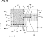
- FIG. 25 is a sectional view of a semiconductor device in Modification 3 of Embodiment 2, along A-A line in FIG. 1 , and corresponds to FIG. 4 .
- FIG. 26 is an enlarged view of part B8 of the semiconductor device shown in FIG. 25 .
- the second skirt portion 8a has a sixth protrusion 86 protruding from the fifth protrusion 85 toward the mounting surface side (Y direction in the drawing) of the lead frame 2, and an eighth bent portion R8 is formed at the sixth protrusion 86.
- Part from the seventh bent portion R7 to the eighth bent portion R8 is a seventh joining portion J7 between the first skirt portion 7a and the second skirt portion 8a.
- the creeping distance from the lead frame 2 to the heatsink 50 is the sum of the distance from the first end T1 to the fourth bent portion R4, the distance from the fourth bent portion R4 to the fifth bent portion R5, the distance from the fifth bent portion R5 to the sixth bent portion R6, the distance from sixth bent portion R6 to the seventh bent portion R7, the distance from the seventh bent portion R7 to the eighth bent portion R8, the distance from the eighth bent portion R8 to a bent portion R63, the distance from the bent portion R63 to a bent portion R64, and the distance from the bent portion R64 to the second end T2, and thus is longer than the creeping distance L1 in the semiconductor device shown in FIG. 6 and FIG. 7 .
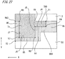
- the heatsink 50 may be jointed to the heat dissipation surface side of the fifth protrusion 85 of the second skirt portion 8a.
- the creeping distance from the lead frame 2 to the heatsink 50 is the sum of the distance from the first end T1 to the fourth bent portion R4, the distance from the fourth bent portion R4 to the fifth bent portion R5, the distance from the fifth bent portion R5 to the sixth bent portion R6, the distance from the sixth bent portion R6 to the seventh bent portion R7, the distance from the seventh bent portion R7 to the eighth bent portion R8, the distance from the eighth bent portion R8 to the bent portion R63, and the distance from the bent portion R63 to the second end T2, and thus is longer than the creeping distance L1 in the semiconductor device shown in FIG. 6 and FIG. 7 .
- the creeping distance from the lead frame to the heatsink is increased as compared to a conventional one, whereby insulation performance is improved.
- FIG. 28 is a sectional view of the semiconductor device in the present Embodiment 3, along A-A line in FIG. 1 , and corresponds to FIG. 4 .
- FIG. 29 is an enlarged view of part B9 of the semiconductor device shown in FIG. 28 .
- the second skirt portion 8a has, at an end of the thin molded portion 8b, a first slope portion 810 expanding toward the heat dissipation surface side of the thin molded portion 8b, and the first skirt portion 7a has a second wraparound portion 710 formed between the first slope portion 810 and the heat dissipation surface 2b of the lead frame 2.
- a ninth bent portion R9 is formed at an end of the first slope portion 810 of the second skirt portion 8a. Part from the first end T1 to the ninth bent portion R9 is an eighth joining portion J8 between the first skirt portion 7a and the second skirt portion 8a.
- the creeping distance from the lead frame 2 to the heatsink 50 is the sum of the distance from the first end T1 to the ninth bent portion R9 and the distance from the ninth bent portion R9 to the second end T2, and thus is longer than the creeping distance (L1) in the semiconductor device shown in FIG. 6 and FIG. 7 . Accordingly, insulation performance is improved.
- FIG. 30 is a sectional view of the semiconductor device in the present Embodiment 4, along A-A line in FIG. 1 , and corresponds to FIG. 4 .
- FIG. 31 is an enlarged view of part B10 of the semiconductor device shown in FIG. 30 .
- the second skirt portion 8a has a first straight portion 820 formed by extending the heat dissipation surface of the lead frame 2 from the first end T1, and has a tenth bent portion R10 at the first straight portion 820. Further, the second skirt portion 8a has a second slope portion 830 extending with an acute angle from the tenth bent portion R10 to the second end T2. Part from the first end T1 to the tenth bent portion RIO is a tenth joining portion J10 between the first skirt portion 7a and the second skirt portion 8a, and part from the tenth bent portion RIO to the second end T2 is an eleventh joining portion J11 between the first skirt portion 7a and the second skirt portion 8a.
- the creeping distance from the lead frame 2 to the heatsink 50 is the sum of the distance from the first end T1 to the tenth bent portion R10 and the distance from the tenth bent portion R10 to the second end T2, and thus is longer than the creeping distance (L1) in the semiconductor device shown in FIG. 6 and FIG. 7 . Accordingly, insulation performance is improved.
- the semiconductor device having high adhesiveness between the thin molded portion and the lead frame can be obtained.
- Embodiment 5 of the present invention will be described with reference to the drawings.
- the entire configuration of the semiconductor device in the present embodiment is the same as that of the semiconductor device according to Embodiment 1, and therefore mainly, only differences will be described.
- parts that are the same as or correspond to those in Embodiment 1 are denoted by the same reference characters.
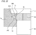
- FIG. 32 is a sectional view of the semiconductor device in the present Embodiment 5, along A-A line in FIG. 1 , and corresponds to FIG. 4 .
- FIG. 33 is an enlarged view of part B11 of the semiconductor device shown in FIG. 32 .
- the second skirt portion 8a has a projection 840 formed in a projecting shape at an end of the thin molded portion 8b, and a twelfth bent portion R12 is formed at the projection 840.
- a twelfth joining portion J12 Part from the first end T1 through the twelfth bent portion R12 to the second end T2 is a twelfth joining portion J12 between the first skirt portion 7a and the second skirt portion 8a. Since the second skirt portion 8a has the projection 840, in the case of using a mold of a type in which dies are opened in the up-down direction, the mold is caught by the projection 840.
- the second skirt portion 8a is formed using a mold having a mechanism such as a slide core that is movable in the right-left direction in the drawing and allows mold release without being caught by the projection 840.
- the first skirt portion 7a is formed using a mold having a mechanism such as a slide core that is movable in the front-back direction in the drawing and allows mold release without being caught by the recess of the first skirt portion 7a that is opposed to the projection 840.
- the creeping distance from the lead frame 2 to the heatsink 50 is the sum of the distance from the first end T1 to the twelfth bent portion R12 and the distance from the twelfth bent portion R12 to the second end T2, and thus is longer than the creeping distance (L1) in the semiconductor device shown in FIG. 6 and FIG. 7 . Accordingly, insulation performance is improved.
- the semiconductor device having high adhesiveness between the thin molded portion 8b and the lead frame 2 can be obtained.
- FIG. 34 is a sectional view of a semiconductor device in another example of the present Embodiment 5, along A-A line in FIG. 1 , and corresponds to FIG. 4 .
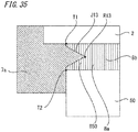
- FIG. 35 is an enlarged view of part B12 of the semiconductor device shown in FIG. 34 .
- the second skirt portion 8a has a recess 850 formed in a recessed shape at an end of the thin molded portion 8b, and a thirteenth bent portion R13 is formed at the recess 850. Part from the first end T1 through the thirteenth bent portion R13 to the second end T2 is a thirteenth joining portion J13 between the first skirt portion 7a and the second skirt portion 8a. Since the second skirt portion 8a has the recess 850, in the case of using a mold of a type in which dies are opened in the up-down direction, the mold is caught by the recess 850.
- the second skirt portion 8a is formed using a mold having a mechanism such as a slide core that is movable in the right-left direction in the drawing and allows mold release without being caught by the recess 850.
- the first skirt portion 7a is formed using a mold having a mechanism such as a slide core that is movable in the front-back direction in the drawing and allows mold release without being caught by the projection of the first skirt portion 7a that is opposed to the recess 850.
- the creeping distance from the lead frame 2 to the heatsink 50 is the sum of the distance from the first end T1 to the thirteenth bent portion R13 and the distance from the thirteenth bent portion R13 to the second end T2, and thus is longer than the creeping distance (L1) in the semiconductor device shown in FIG. 6 and FIG. 7 . Accordingly, insulation performance is improved.
- the semiconductor device having high adhesiveness between the thin molded portion 8b and the lead frame 2 can be obtained.
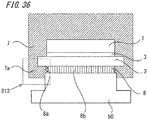
- FIG. 36 is a sectional view of a semiconductor device in another example of the present Embodiment 5, along A-A line in FIG. 1 , and corresponds to FIG. 4 .
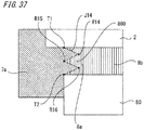
- FIG. 37 is an enlarged view of part B13 in the semiconductor device shown in FIG. 36 .
- the second skirt portion 8a has a recessed and projecting portion 860 formed in a recessed and projecting shape at an end of the thin molded portion 8b, and a plurality of bent portions (fourteenth bent portion R14, fifteenth bent portion R15, sixteenth bent portion R16) are formed at the recessed and projecting portion 860.
- a fourteenth joining portion J14 Part from the first end T1 through the plurality of bent portions (fourteenth bent portion R14, fifteenth bent portion R15, sixteenth bent portion R16) to the second end T2 is a fourteenth joining portion J14 between the first skirt portion 7a and the second skirt portion 8a. Since the second skirt portion 8a has the recessed and projecting portion 860, in the case of using a mold of a type in which dies are opened in the up-down direction, the mold is caught by the recessed and projecting portion 860.
- the second skirt portion 8a is formed using a mold having a mechanism such as a slide core that is movable in the right-left direction in the drawing and allows mold release without being caught by the recessed and projecting portion 860.
- the first skirt portion 7a is formed using a mold having a mechanism such as a slide core that is movable in the front-back direction in the drawing and allows mold release without being caught by the recessed and projecting portion 860.
- the creeping distance from the lead frame 2 to the heatsink 50 is a distance from the first end T1 through the plurality of bent portions (fourteenth bent portion R14, fifteenth bent portion R15, sixteenth bent portion R16) to the second end T2, and thus is longer than the creeping distance (L1) in the semiconductor device shown in FIG. 6 and FIG. 7 . Accordingly, insulation performance is improved.
- the semiconductor device having high adhesiveness between the thin molded portion 8b and the lead frame 2 can be obtained.
- a semiconductor device according to the present embodiment is a modification of the semiconductor devices according to the above embodiments, and the entire configuration thereof is the same. Therefore, only differences will be described.
- parts that are the same as or correspond to those in the above embodiment are denoted by the same reference characters.
- FIG. 38 is a sectional view of the semiconductor device in the present embodiment, along A-A line in FIG. 1 , and corresponds to FIG. 4 in Embodiment 1.
- FIG. 39 is an enlarged view of part B14 of the semiconductor device shown in FIG. 38 , and corresponds to FIG. 5 in Embodiment 1.
- the outer peripheral surface part of the second skirt portion 8a has the first end T1 connected to the lead frame 2 and the first skirt portion 7a, and the second end T2 connected to the heatsink 50. Between the first end T1 and the second end T2, the first bent portion R1 and a last bent portion RLast are formed. It is noted that the last bent portion RLast means a last bent portion as counted from the first end T1.
- part from the second end T2 to the last bent portion RLast is sloped in such a direction as to be separated from the opposed surface (side surface portion 50A) of the heatsink 50.
- part from the first end T1 to the second end T2 of the second skirt portion 8a is not in contact with the heatsink 50.
- the last bent portion RLast has an angular shape, but may have a round curved-surface shape.
- part from the first end T1 to the first bent portion R1 is sloped in such a direction as to be separated from the opposed surface (side surface portion 50A) of the heatsink 50, but may not have a sloped shape.
- the creeping distance from the lead frame 2 to the heatsink 50 is the sum (L10 + L20 + L30) of a distance L10 from the first end T1 to the first bent portion R1, a distance L20 from the first bent portion R1 to the last bent portion RLast, and a distance L30 from the last bent portion RLast to the second end T2, and thus is longer than the creeping distance (L1 + L2) in the semiconductor device shown in FIG. 4 and FIG. 5 .
- This configuration is effective in the case where the sum (L20 + L30) of the distance L20 and the distance L30 is greater than a distance L40 between a side-surface protrusion 50B of the heatsink 50, and the first skirt portion 7a and the second skirt portion 8a.
- a distance L40 between a side-surface protrusion 50B of the heatsink 50, and the first skirt portion 7a and the second skirt portion 8a.
- part from the second end T2 to the last bent portion RLast of the outer peripheral surface part of the second skirt portion 8a has a sloped shape, whereby an effect of facilitating mold release is obtained.
- Embodiment 6 an example corresponding to the semiconductor device shown in FIG. 4 and FIG. 5 in Embodiment 1 has been described.
- the above configuration is also applicable to FIG. 8 , FIG. 9 , FIG. 10 , FIG. 11 and FIG. 12 , FIG. 13 , FIG. 14 and FIG. 15 , and FIG. 16 in Embodiment 1.
- the above configuration is also applicable to FIG. 19 and FIG. 20 , FIG. 21 , FIG. 22 and FIG. 23 , FIG. 24 , FIG. 25 and FIG. 26 , and FIG. 27 in Embodiment 2.
- a semiconductor device according to the present embodiment is a modification of the semiconductor devices according to the above embodiments 1 to 6, and the entire configuration thereof is the same. Therefore, only differences will be described.
- the joining surfaces of the first skirt portion 7a and the second skirt portion 8a in the semiconductor devices of the above embodiments 1 to 6 are roughened. Roughening the joining surfaces of the first skirt portion 7a and the second skirt portion 8a improves adhesiveness between the first skirt portion 7a and the second skirt portion 8a, leading to improvement in insulation performance. In addition, a semiconductor device having high heat dissipation property and improved reliability is obtained.
- the mold surface roughness of the first skirt portion 7a or the second skirt portion 8a that is first formed by transfer molding may be set to about 20 or greater in Rz (ten-point average roughness), whereby the same effects are obtained.
Landscapes
- Structures Or Materials For Encapsulating Or Coating Semiconductor Devices Or Solid State Devices (AREA)
- Cooling Or The Like Of Semiconductors Or Solid State Devices (AREA)
- Chemical & Material Sciences (AREA)
- Engineering & Computer Science (AREA)
- Materials Engineering (AREA)
Abstract
Description
- The present invention relates to a semiconductor device of a resin-molded type.
- In a semiconductor device for power or the like, a semiconductor element such as an insulated gate bipolar transistor (IGBT), a metal-oxide-semiconductor field-effect transistor (MOSFET), an integrated circuit (IC) chip, or a large scale integrated circuit (LSI) chip is die-bonded to a lead frame for external terminal, and then electrically connected to a wire by a wire bond process or an inner lead such as a copper plate or a copper alloy by soldering, thereby allowing input and output of signals from and to the outside.
- In a semiconductor device of a resin-molded type, a surface (mounting surface) of a lead frame on the side where a semiconductor element is mounted and a heat dissipation surface on the opposite side are sealed by an insulation resin using transfer molding. In particular, as for a semiconductor device for power, a semiconductor element that generates a large amount of heat is provided inside, and therefore an insulation resin for sealing is required to have high thermal conductivity. Accordingly, a semiconductor device is proposed in which, in a molding resin sealing process, the heat dissipation surface side is sealed by a high heat dissipation conductive resin having a thermal conductivity of 3 W/m·K to 10 W/m·K, and the mounting surface side is sealed by a low-stress resin or the like.
- Here, molding with two types of resins, i.e., the resin for the mounting surface side and the resin for the heat dissipation surface side forms an interface between the two types of resins. An electric field is likely to concentrate on the interface, and the interface has poor adhesiveness, which causes peeling, leading to a problem that insulation property is deteriorated.
- In order to solve the problem, there is technology disclosed in
Patent Document 1 below. A semiconductor device ofPatent Document 1 includes: a plate-like lead frame having first and second main surfaces and a pattern shape and having an external terminal therearound; a semiconductor element fixed on the first main surface; a heatsink provided so as to be opposed to the second main surface with a gap therebetween; and sealing resin for sealing the semiconductor element, the lead frame, and the heatsink. - The sealing resin includes a primary sealing resin and a secondary sealing resin having higher thermal conductivity than the primary sealing resin. The secondary sealing resin has: a part that is in close contact with the second main surface and fills the gap between the lead frame and the heatsink; and a protrusion integrally connected to the above part and penetrating a gap of the lead frame accompanying the pattern shape, to protrude in a wall shape toward the first main surface side. The primary sealing resin is in close contact with the first main surface and encloses the semiconductor element, and also is in close contact with the protrusion.
- Patent Document 1: Japanese Laid-Open Patent Publication
JP 9-153 572 A - In
Patent Document 1, the creeping distance between parts of the lead frame that are adjacent to each other via a gap, along the interface between the primary sealing resin and the secondary sealing resin, is increased, whereby insulation performance of the parts of the lead frame is improved, leading to an effect of improving withstand voltage. - However, in
Patent Document 1, the creeping distance between the lead frame and the heatsink along the interface between the primary sealing resin and the secondary sealing resin is not taken into consideration. - The present invention has been made to solve the above problems, and an object of the present invention is to provide a semiconductor device that has a longer creeping distance between a lead frame and a heatsink than a conventional one and thus has improved insulation performance.
- A semiconductor device according to the present invention includes: a lead frame with a semiconductor element mounted thereto; a first insulation resin portion formed on a mounting surface side of the lead frame on which the semiconductor element is mounted; a second insulation resin portion formed on a heat dissipation surface side of the lead frame which is opposite to the mounting surface side; and a heatsink fixed to a heat dissipation surface of the second insulation resin portion, wherein the second insulation resin portion has a thin molded portion in close contact with the lead frame, and a second skirt portion formed at an end of the thin molded portion, the first insulation resin portion has a first skirt portion protruding toward the heat dissipation surface side of the lead frame and covering the second skirt portion of the second insulation resin portion, and an outer peripheral surface part of the second skirt portion has a first end connected to the lead frame and the first skirt portion, a second end connected to the heatsink, and at least one bent portion formed between the first end and the second end.
- The semiconductor device according to the present invention has a longer creeping distance from the lead frame to the heatsink than a conventional one and thus has improved insulation performance.
-
- FIG. 1
- is a side sectional view showing the configuration of a semiconductor device according to
Embodiment 1 of the present invention. - FIG. 2
- is a schematic plan view of the semiconductor device after a first-time transfer molding step, as seen from the heat dissipation surface side, in
Embodiment 1 of the present invention. - FIG. 3
- is a schematic plan view of the semiconductor device after a second-time transfer molding step, as seen from the heat dissipation surface side in
Embodiment 1 of the present invention. - FIG. 4
- is a sectional view along A-A line of the semiconductor device shown in
FIG. 1 . - FIG. 5
- is an enlarged view of part B1 of the semiconductor device shown in
FIG. 4 . - FIG. 6
- is a view of a semiconductor device in a comparative example of
Embodiment 1 and corresponds toFIG. 4 . - FIG. 7
- is an enlarged view of part C of the semiconductor device shown in
FIG. 6 . - FIG. 8
- is an enlarged view of a part of a semiconductor device in
Modification 1 ofEmbodiment 1. - FIG. 9
- is an enlarged view of a part of a semiconductor device in
Modification 2 ofEmbodiment 1. - FIG. 10
- is an enlarged view of a part of a semiconductor device in
Modification 3 ofEmbodiment 1. - FIG. 11
- is a sectional view of a semiconductor device in
Modification 4 ofEmbodiment 1, along A-A line inFIG. 1 . - FIG. 12
- is an enlarged view of part B3 of the semiconductor device shown in
FIG. 11 . - FIG. 13
- is an enlarged view of a part of the semiconductor device in
Modification 4 ofEmbodiment 1. - FIG. 14
- is a sectional view of a semiconductor device in
Modification 5 ofEmbodiment 1, along A-A line inFIG. 1 . - FIG. 15
- is an enlarged view of part B4 of the semiconductor device shown in
FIG. 14 . - FIG. 16
- is an enlarged view of a part of the semiconductor device in
Modification 5 ofEmbodiment 1. - FIG. 17
- is a sectional view of a semiconductor device in
Embodiment 2 of the present invention, along A-A line inFIG. 1 . - FIG. 18
- is an enlarged view of part B5 of the semiconductor device shown in
FIG. 17 . - FIG. 19
- is a sectional view of a semiconductor device in
Modification 1 ofEmbodiment 2, along A-A line inFIG. 1 . - FIG. 20
- is an enlarged view of part B6 of the semiconductor device shown in
FIG. 19 . - FIG. 21
- is an enlarged view of a part of the semiconductor device in
Modification 1 ofEmbodiment 2. - FIG. 22
- is a sectional view of a semiconductor device in
Modification 2 ofEmbodiment 2, along A-A line inFIG. 1 . - FIG. 23
- is an enlarged view of part B7 of the semiconductor device shown in
FIG. 22 . - FIG. 24
- is an enlarged view of a part of the semiconductor device in
Modification 2 ofEmbodiment 2. - FIG. 25
- is a sectional view of a semiconductor device in
Modification 3 ofEmbodiment 2, along A-A line inFIG. 1 . - FIG. 26
- is an enlarged view of part B8 of the semiconductor device shown in
FIG. 25 . - FIG. 27
- is an enlarged view of a part of the semiconductor device in
Modification 3 ofEmbodiment 2. - FIG. 28
- is a sectional view of a semiconductor device in
Embodiment 3 of the present invention, along A-A line inFIG. 1 . - FIG. 29
- is an enlarged view of part B9 of the semiconductor device shown in
FIG. 28 . - FIG. 30
- is a sectional view of a semiconductor device in
Embodiment 4 of the present invention, along A-A line inFIG. 1 . - FIG. 31
- is an enlarged view of part B10 of the semiconductor device shown in
FIG. 30 . - FIG. 32
- is a sectional view of a semiconductor device in
Embodiment 5 of the present invention, along A-A line inFIG. 1 . - FIG. 33
- is an enlarged view of part B11 of the semiconductor device shown in
FIG. 32 . - FIG. 34
- is a sectional view of a semiconductor device in another example of
Embodiment 5 of the present invention, along A-A line inFIG. 1 . - FIG. 35
- is an enlarged view of part B12 of the semiconductor device shown in
FIG. 34 . - FIG. 36
- is a sectional view of a semiconductor device in another example of
Embodiment 5 of the present invention, along A-A line inFIG. 1 . - FIG. 37
- is an enlarged view of part B13 of the semiconductor device shown in
FIG. 36 . - FIG. 38
- is a sectional view of a semiconductor device in
Embodiment 6 of the present invention, along A-A line inFIG. 1 . - FIG. 39
- is an enlarged view of part B14 of the semiconductor device shown in
FIG. 38 . - Hereinafter, a semiconductor device according to
Embodiment 1 of the present invention will be described with reference to the drawings.FIG. 1 is a side sectional view showing the configuration of a semiconductor device according to thepresent Embodiment 1,FIG. 2 is a schematic plan view of the semiconductor device in which a first insulation resin portion is formed in a first-time transfer molding step, as seen from the heat dissipation surface side. -
FIG. 3 is a schematic plan view of the semiconductor device in which a second insulation resin portion is formed in a second-time transfer molding step, as seen from the heat dissipation surface side,FIG. 4 is a sectional view along A-A line of the semiconductor device shown inFIG. 1 , andFIG. 5 is an enlarged view of part B1 of the semiconductor device shown inFIG. 4 . InFIG. 2 andFIG. 3 , a heatsink is not shown. In the drawings, the same or corresponding parts are denoted by the same reference characters. - As shown in the drawings, a
semiconductor device 100 according to thepresent Embodiment 1 includes asemiconductor element 1, alead frame 2, anexternal terminal 4, awire 5, aninner lead 6, a firstinsulation resin portion 7, a secondinsulation resin portion 8, and aheatsink 50. InFIG. 1 , thesemiconductor element 1 such as IGBT, MOSFET, IC chip, or LSI chip is mounted above a surface (hereinafter, referred to as mountingsurface 2a) of thelead frame 2 that is on the upper side in the drawing, with a joiningmember 3 such as solder or silver interposed therebetween. Thelead frame 2 is made from a copper plate, a copper alloy plate, or the like, and the surface of thelead frame 2 is coated by metallic plating of gold, silver, nickel, tin, or the like (not shown). - An electrode pad of the
semiconductor element 1 is electrically connected to theexternal terminal 4 via thewire 5 connected by wire bonding, or via theinner lead 6 made from a material such as a copper plate or a copper alloy plate, and thesemiconductor element 1 performs input and output of signals from and to an external device via theexternal terminal 4. - The
wire 5 is made from gold, silver, aluminum, copper, or the like, and the wire diameter thereof is about 20 µm to 500 µm. Theinner lead 6 is joined to thesemiconductor element 1 or thelead frame 2 via a joiningmember 3 such as solder or silver. It is noted that thewire 5 and theinner lead 6 are replaceable with each other. - The first
insulation resin portion 7 made from a first insulation resin is formed on the mountingsurface 2a side of thelead frame 2. The secondinsulation resin portion 8 made from a second insulation resin is formed on theheat dissipation surface 2b side of thelead frame 2 which is opposite to the mountingsurface 2a. A part 10 (hereinafter, referred to as die pad interval part 10) between two separate areas of thelead frame 2 is filled with the first insulation resin, to form the firstinsulation resin portion 7. - The second
insulation resin portion 8 has a thin moldedportion 8b formed in contact with theheat dissipation surface 2b of thelead frame 2. The thickness of the thin moldedportion 8b is about 0.02 mm to 0.3 mm. Theheatsink 50 made of copper, aluminum, or the like is joined, via a heat dissipation member such as grease or by resin molding, to a heat dissipation surface 8b2 of the thin moldedportion 8b which is opposite to a lead frame joining surface 8b1 in contact with thelead frame 2. - The insulation resins forming the first
insulation resin portion 7 and the secondinsulation resin portion 8 are both thermosetting epoxy resin or the like. It is noted that the secondinsulation resin portion 8 formed on theheat dissipation surface 2b side of thelead frame 2 is made of an insulation resin having higher thermal conductivity than the firstinsulation resin portion 7 formed on the mountingsurface 2a side. The second insulation resin forming the secondinsulation resin portion 8 contains a filler such as silica, alumina, boron nitride, or aluminum nitride having high thermal conductivity, and the thermal conductivity of the secondinsulation resin portion 8 is 3 W/m·K to 12 W/m·K. - For the first
insulation resin portion 7 on the mountingsurface 2a side, a low-stress insulation resin having great fluidity, which is used for a general semiconductor device, is used. For example, a low-stress insulation resin obtained by adding silicone to a thermosetting epoxy resin or the like, or a low-stress insulation resin having a thermal expansion coefficient close to that of the lead frame, is used. - As shown in
FIG. 4 andFIG. 5 , at the outer peripheral end part on theheat dissipation surface 2b side of thelead frame 2, afirst skirt portion 7a formed from the first insulation resin and asecond skirt portion 8a formed from the second insulation resin are provided. That is, the secondinsulation resin portion 8 has the thin moldedportion 8b having a thickness of about 0.02 mm to 0.3 mm and formed in close contact with theheat dissipation surface 2b of thelead frame 2, and thesecond skirt portion 8a having afirst protrusion 81 protruding from an end of the thin moldedportion 8b toward the heat dissipation surface 8b2 side of the secondinsulation resin portion 8. The firstinsulation resin portion 7 has thefirst skirt portion 7a protruding toward theheat dissipation surface 2b side of thelead frame 2 and covering thesecond skirt portion 8a. - The
first skirt portion 7a and thesecond skirt portion 8a have protrusion shapes such that the virtual-direction thicknesses thereof from theheat dissipation surface 2b of thelead frame 2 are about 0.3 mm to 2 mm which is thicker than the thickness of the thin moldedportion 8b. - As shown in
FIG. 5 , thesecond skirt portion 8a has, at an outer peripheral surface part thereof: a first end T1 connected to thelead frame 2 and thefirst skirt portion 7a; a second end T2 connected to theheatsink 50; and at least one bent portion formed between the first end T1 and the second end T2, i.e., a first bent portion R1 formed at thefirst protrusion 81. Part from the first end T1 to the first bent portion R1 forms a first joining portion J1 between thefirst skirt portion 7a and thesecond skirt portion 8a. - In
FIG. 5 , part from the first end T1 to the first bent portion R1 is shown in a straight shape, and part from the first bent portion R1 to the second end T2 is shown in a straight shape. These parts shown in straight shapes have flat plane shapes. However, in actuality, thefirst skirt portion 7a and thesecond skirt portion 8a are molded with resin by transfer molding, and thus these plane shapes have irregularity to a certain degree. In addition, in the drawings for other examples of the present invention shown below, part between the first end and the bent portion, part between the bent portions, and part between the bent portion and the second end, which are shown in straight shapes, have flat plane shapes as in the above case. - In
FIG. 5 , the first bent portion R1 is shown in a rectangular shape. However, in actuality, thesecond skirt portion 8a is molded with resin by transfer molding and thus has a curved part or irregularity to a certain degree. - Next, the creeping distance from the
lead frame 2 to theheatsink 50 in thesemiconductor device 100 of thepresent Embodiment 1 will be described. -
FIG. 6 is a sectional view of a semiconductor device in a comparative example of the present embodiment, along A-A line inFIG. 1 , and corresponds toFIG. 4 .FIG. 7 is an enlarged view of part B2 of the semiconductor device shown inFIG. 6 . - The semiconductor device in the comparative example shown in
FIG. 6 andFIG. 7 does not have thesecond skirt portion 8a protruding from an end of the thin moldedportion 8b toward the heat dissipation surface side as in the present embodiment, and a creeping distance L from thelead frame 2 to theheatsink 50 is a distance L3 from the first end T1 connected to thelead frame 2, thefirst skirt portion 7a, and the thin moldedportion 8b, to the second end T2 connected to theheatsink 50, thefirst skirt portion 7a, and the thin moldedportion 8b. - On the other hand, in the semiconductor device of the present embodiment, as shown in
FIG. 5 , a creeping distance L from thelead frame 2 to theheatsink 50 is the sum (L = L1 + L2) of a distance L1 from the first end T1 connected to thelead frame 2, thefirst skirt portion 7a, and the second skirt portion (first protrusion) 8a, to the first bent portion R1 formed at thesecond skirt portion 8a (first protrusion 81), and a distance L2 from the first bent portion R1 to the second end T2 connected to theheatsink 50 and the second skirt portion (first protrusion) 8a. It is noted that part from the first end T1 to the first bent portion R1 is the first joining portion J1 which is the interface between thefirst skirt portion 7a and thesecond skirt portion 8a. - As described above, in the semiconductor device of the present embodiment, the creeping distance from the
lead frame 2 to theheatsink 50 is greatly increased and insulation property is improved, as compared to the semiconductor device in the comparative example shown inFIG. 6 andFIG. 7 . - Also in comparison with the semiconductor device shown in
FIG. 9 ofPatent Document 1 described above, the creeping distance from the lead frame to the heatsink in the semiconductor device of the present Embodiment is increased and thus insulation property is improved. - That is, in
FIG. 9 ofPatent Document 1, the creeping distance from the lead frame to the heatsink extends in a straight line via the interface of the primary sealing resin and the secondary sealing resin, whereas the creeping distance in the present embodiment extends from the first end T1 of thelead frame 2 via the first bent portion R1 to the second end T2 of theheatsink 50. Therefore, the creeping distance is increased and insulation property is also improved. - In the sectional view of the semiconductor device shown in
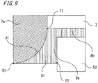
FIG. 4 andFIG. 5 , the outer peripheral surface part of thesecond skirt portion 8a is formed in a straight line extending from the first end T1 toward the heat dissipation side to reach the first bent portion R1. However, as shown inFIG. 8 , the outer peripheral surface part of thesecond skirt portion 8a may be sloped outward from the first end T1 to the first bent portion R1. - In this case, the
second skirt portion 8a has a trapezoidal shape, and the creeping distance from thelead frame 2 to theheatsink 50 is the sum (L4 + L5) of a distance L4 from the first end T1 to the first bent portion R1 and a distance L5 from the first bent portion R1 to the second end T2, and thus is longer than the creeping distance (L1 + L2) in the semiconductor device shown inFIG. 4 andFIG. 5 . - As shown in
FIG. 9 , the outer peripheral surface part of thesecond skirt portion 8a may be formed in an arc shape expanding outward from the first end T1 to the first bent portion R1. Also in this case, the creeping distance from thelead frame 2 to theheatsink 50 is the sum of the distance from the first end T1 to the first bent portion R1 and the distance from the first bent portion R1 to the second end T2, and thus is longer than the creeping distance (L1 + L2) in the semiconductor device shown inFIG. 4 andFIG. 5 . - As shown in
FIG. 10 , aside surface portion 50A of theheatsink 50 may be separated from one side surface portion 8a1 of thesecond skirt portion 8a. In such a configuration, the creeping distance from thelead frame 2 to theheatsink 50 is the sum of the distance from the first end T1 to the first bent portion R1, the distance from the first bent portion R1 to a bent portion R50, the distance from the bent portion R50 to a bent portion R51, and the distance from the bent portion R51 to the second end T2, and thus is longer than the creeping distance (L1 + L2) in the semiconductor device shown inFIG. 4 andFIG. 5 . -
FIG. 11 is a sectional view of a semiconductor device inModification 4 of the present embodiment, along A-A line inFIG. 1 , and corresponds toFIG. 4 .FIG. 12 is an enlarged view of part B3 of the semiconductor device shown inFIG. 11 . - In
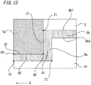
FIG. 11 andFIG. 12 , thesecond skirt portion 8a has thefirst protrusion 81 protruding toward the heat dissipation surface 8b2 side of the thin moldedportion 8b, and asecond protrusion 82 protruding from thefirst protrusion 81 toward the side surface (X direction in the drawing) of thesemiconductor device 100, and further has the first bent portion R1 formed at thefirst protrusion 81 and a second bent portion R2 formed at thesecond protrusion 82. - Part from the first end T1 to the first bent portion R1 is the first joining portion J1 between the
first skirt portion 7a and thesecond skirt portion 8a, and part from the first bent portion R1 to the second bent portion R2 is a second joining portion J2 between thefirst skirt portion 7a and thesecond skirt portion 8a. That is, thesecond skirt portion 8a is formed so as to cover the inner side surface and a surface that is on the lower side in the drawing, of thefirst skirt portion 7a. - In such a configuration, the creeping distance from the
lead frame 2 to theheatsink 50 is the sum of the distance from the first end T1 to the first bent portion R1, the distance from the first bent portion R1 to the second bent portion R2, the distance from the second bent portion R2 to a bent portion R52, and the distance from the bent portion R52 to the second end T2, and thus is longer than the creeping distance (L1 + L2) in the semiconductor device shown inFIG. 4 andFIG. 5 . - As shown in
FIG. 13 , theheatsink 50 may be joined to the heat dissipation surface side of thesecond protrusion 82 of thesecond skirt portion 8a. Also in this case, the creeping distance from thelead frame 2 to theheatsink 50 is the sum of the distance from the first end T1 to the first bent portion R1, the distance from the first bent portion R1 to the second bent portion R2, and the distance from the second bent portion R2 to the second end T2, and thus is longer than the creeping distance (L1 + L2) in the semiconductor device shown inFIG. 4 andFIG. 5 . -
FIG. 14 is a sectional view of a semiconductor device inModification 5 of the present embodiment, along A-A line inFIG. 1 , and corresponds toFIG. 4 .FIG. 15 is an enlarged view of part B4 of the semiconductor device shown inFIG. 14 . - In
FIG. 14 andFIG. 15 , thesecond skirt portion 8a has thefirst protrusion 81 protruding toward the heat dissipation surface 8b2 side of the thin moldedportion 8b, thesecond protrusion 82 protruding from thefirst protrusion 81 toward the side surface (X direction in the drawing) of thesemiconductor device 100, and athird protrusion 83 protruding toward the mounting surface side of thelead frame 2 from thesecond protrusion 82, and further has the first bent portion R1 formed at thefirst protrusion 81, the second bent portion R2 formed at thesecond protrusion 82, and a third bent portion R3 formed at thethird protrusion 83. - Part from the first end T1 to the first bent portion R1 is the first joining portion J1 between the
first skirt portion 7a and thesecond skirt portion 8a, part from the first bent portion R1 to the second bent portion R2 is the second joining portion J2 between thefirst skirt portion 7a and thesecond skirt portion 8a, and part from the second bent portion R2 to the third bent portion R3 is a third joining portion J3 between thefirst skirt portion 7a and thesecond skirt portion 8a. That is, thesecond skirt portion 8a is formed so as to cover the inner side surface, the outer side surface, and a surface that is on the lower side in the drawing, of thefirst skirt portion 7a. - In such a configuration, the creeping distance from the
lead frame 2 to theheatsink 50 is the sum of the distance from the first end T1 to the first bent portion R1, the distance from the first bent portion R1 to the second bent portion R2, the distance from the second bent portion R2 to the third bent portion R3, the distance from the third bent portion R3 to a bent portion R53, the distance from the bent portion R53 to a bent portion R54, and the distance from the bent portion R54 to the second end T2, and thus is longer than the creeping distance (L1 + L2) in the semiconductor device shown inFIG. 4 andFIG. 5 . - As shown in
FIG. 16 , theheatsink 50 may be joined to the heat dissipation surface side of thesecond protrusion 82 of thesecond skirt portion 8a. Also in this case, the creeping distance from thelead frame 2 to theheatsink 50 is the sum of the distance from the first end T1 to the first bent portion R1, the distance from the first bent portion R1 to the second bent portion R2, the distance from the second bent portion R2 to the third bent portion R3, the distance from the third bent portion R3 to the bent portion R53, and the distance from the bent portion R53 to the second end T2, and thus is longer than the creeping distance (L1 + L2) in the semiconductor device shown inFIG. 4 andFIG. 5 . - As described above, in the present embodiment, the semiconductor device includes: a lead frame with a semiconductor element mounted thereto; a first insulation resin portion formed on the mounting surface side of the lead frame on which the semiconductor element is mounted; a second insulation resin portion formed on the heat dissipation surface side of the lead frame which is opposite to the mounting surface side; and a heatsink fixed to the heat dissipation surface side of the second insulation resin portion. The second insulation resin portion has a thin molded portion in close contact with the lead frame, and a second skirt portion formed at an end of the thin molded portion.
- The first insulation resin portion has a first skirt portion protruding toward the heat dissipation surface side of the lead frame and covering the second skirt portion of the second insulation resin portion. The outer peripheral surface part of the second skirt portion has a first end connected to the lead frame and the first skirt portion, a second end connected to the heatsink, and at least one bent portion formed between the first end and the second end. Therefore, the creeping distance from the lead frame to the heatsink is increased as compared to a conventional one, whereby insulation performance is improved.
- In addition, the protrusion-direction thicknesses of the first skirt portion and the second skirt portion are greater than the thickness of the thin molded portion. Therefore, it is possible to increase the creeping distance between the lead frame and the heatsink by a necessary insulation distance, and prevent decrease in heat dissipation.
- In addition, since the first skirt portion and the second skirt portion are provided, the strength and the insulation distance at an outer peripheral end part of the lead frame to which voltage is applied can be ensured.
- In the present embodiment, the case where the surface of the lead frame is coated by metallic plating of gold, silver, nickel, tin, or the like has been described. However, the surface of the lead frame may not be coated. In the present embodiment, the lead frame has a uniform thickness. However, the lead frame may have a different thickness at some part thereof. In the present embodiment, the case of joining the heatsink to the thin molded portion via a heat dissipation member such as grease has been described. However, a heat dissipation member may not be used.
- In the present embodiment, the mounting surface side of the lead frame may also have the same heat dissipation property as the heat dissipation surface side. For example, a high heat dissipation resin having a thermal conductivity of 3 W/m·K to 12 W/m·K, which is the same as the second insulation resin portion, may be used as the first insulation resin portion. Since the periphery of the semiconductor element which is a heat generating component is sealed by the high heat dissipation resin, heat is dissipated from the entire periphery of the semiconductor element and thus heat dissipation is increased.
- In the present embodiment, as shown in
FIG. 3 , in the semiconductor device having substantially a rectangular shape in a plan view, the first skirt portion formed from the first insulation resin is located on the long side and the second skirt portion formed from the second insulation resin is located on the short side. However, this configuration may be reversed depending on the position of the gate of a molding die to be used. - In the present embodiment, in the semiconductor device having substantially a rectangular shape in a plan view, the positions of the sides formed by the first skirt portion molded with the first insulation resin and the second skirt portion molded with the second insulation resin are not limited to those shown in
FIG. 3 , and also, the number of the sides of each of the first skirt portion and the second skirt portion is not limited to two. - In the present embodiment, the position of a gate break left
part 7b occurring after the first insulation resin portion is molded or the position of a gate break leftpart 8c occurring after the second insulation resin portion is molded, is not limited to that shown inFIG. 1 andFIG. 3 , and also, the number thereof is not limited to one but may be plural. - In the present embodiment, as shown in
FIG. 2 andFIG. 3 , after the first insulation resin portion is molded in the first-time transfer molding step, the second insulation resin portion is molded in the second-time transfer molding step. However, after the second insulation resin portion is molded in the first-time transfer molding step, the first insulation resin portion may be molded in the second-time transfer molding step. - Hereinafter, a semiconductor device according to
Embodiment 2 of the present invention will be described with reference to the drawings. - The entire configuration of the semiconductor device in the present embodiment is the same as that of the semiconductor device according to
Embodiment 1, and therefore mainly, only differences will be described. In the drawings, parts that are the same as or correspond to those inEmbodiment 1 are denoted by the same reference characters. -
FIG. 17 is a sectional view of the semiconductor device in thepresent Embodiment 2, along A-A line inFIG. 1 , and corresponds toFIG. 4 .FIG. 18 is an enlarged view of part B5 of the semiconductor device shown inFIG. 17 . - In the present embodiment, as shown in
FIG. 17 andFIG. 18 , thesecond skirt portion 8a has astep portion 800 extending in parallel with thelead frame 2 from an end of the thin moldedportion 8b, and thefirst skirt portion 7a has afirst wraparound portion 700 formed between thestep portion 800 and theheat dissipation surface 2b of thelead frame 2. A fourth bent portion R4 and a fifth bent portion R5 are formed along a fourth joining portion J4 between thestep portion 800 of thesecond skirt portion 8a and thefirst wraparound portion 700 of thefirst skirt portion 7a. - In the present embodiment, the creeping distance from the
lead frame 2 to theheatsink 50 is the sum of the distance from the first end T1 to the fourth bent portion R4, the distance from the fourth bent portion R4 to the fifth bent portion R5, and the distance from the fifth bent portion R5 to the second end T2, and thus is longer than the creeping distance (L1) in the semiconductor device shown inFIG. 6 andFIG. 7 . Therefore, insulation performance is improved. -
FIG. 19 is a sectional view of a semiconductor device inModification 1 ofEmbodiment 2, along A-A line inFIG. 1 , and corresponds toFIG. 4 .FIG. 20 is an enlarged view of part B6 of the semiconductor device shown inFIG. 19 . - In
FIG. 19 andFIG. 20 , thesecond skirt portion 8a has afourth protrusion 84 protruding from thestep portion 800 toward the heat dissipation surface side of the thin moldedportion 8b, and a sixth bent portion R6 is formed at thefourth protrusion 84. Part from the fifth bent portion R5 to the sixth bent portion R6 is a fifth joining portion J5 between thefirst skirt portion 7a and thesecond skirt portion 8a. - In such a configuration, the creeping distance from the
lead frame 2 to theheatsink 50 is the sum of the distance from the first end T1 to the fourth bent portion R4, the distance from the fourth bent portion R4 to the fifth bent portion R5, the distance from the fifth bent portion R5 to the sixth bent portion R6, and the distance from the sixth bent portion R6 to the second end T2, and thus is longer than the creeping distance L1 in the semiconductor device shown inFIG. 6 andFIG. 7 . - As shown in
FIG. 21 , theside surface portion 50A of theheatsink 50 may be separated from one side surface portion 8a1 of thesecond skirt portion 8a. In such a configuration, the creeping distance from thelead frame 2 to theheatsink 50 is the sum of the distance from the first end T1 to the fourth bent portion R4, the distance from the fourth bent portion R4 to the fifth bent portion R5, the distance from the fifth bent portion R5 to the sixth bent portion R6, the distance from the sixth bent portion R6 to a bent portion R60, the distance from the bent portion R60 to a bent portion R61, and the distance from the bent portion R61 to the second end T2, and thus is longer than the creeping distance L1 in the semiconductor device shown inFIG. 6 andFIG. 7 . -
FIG. 22 is a sectional view of a semiconductor device inModification 2 ofEmbodiment 2, along A-A line inFIG. 1 , and corresponds toFIG. 4 .FIG. 23 is an enlarged view of part B7 of the semiconductor device shown inFIG. 22 . - In
FIG. 22 andFIG. 23 , thesecond skirt portion 8a has afifth protrusion 85 protruding from thefourth protrusion 84 toward the side surface (X direction in the drawing) of thesemiconductor device 100, and a seventh bent portion R7 is formed at thefifth protrusion 85. Part from the sixth bent portion R6 to the seventh bent portion R7 is a sixth joining portion J6 between thefirst skirt portion 7a and thesecond skirt portion 8a. - In such a configuration, the creeping distance from the
lead frame 2 to theheatsink 50 is the sum of the distance from the first end T1 to the fourth bent portion R4, the distance from the fourth bent portion R4 to the fifth bent portion R5, the distance from the fifth bent portion R5 to the sixth bent portion R6, the distance from the sixth bent portion R6 to the seventh bent portion R7, the distance from the seventh bent portion R7 to a bent portion R62, and the distance from the bent portion R62 to the second end T2, and thus is longer than the creeping distance L1 in the semiconductor device shown inFIG. 6 andFIG. 7 . - As shown in
FIG. 24 , theheatsink 50 may be joined to the heat dissipation surface side of thefifth protrusion 85 of thesecond skirt portion 8a. Also in this case, the creeping distance from thelead frame 2 to theheatsink 50 is the sum of the distance from the first end T1 to the fourth bent portion R4, the distance from the fourth bent portion R4 to the fifth bent portion R5, the distance from the fifth bent portion R5 to the sixth bent portion R6, the distance from the sixth bent portion R6 to the seventh bent portion R7, and the distance from the seventh bent portion R7 to the second end T2, and thus is longer than the creeping distance L1 in the semiconductor device shown inFIG. 6 andFIG. 7 . -
FIG. 25 is a sectional view of a semiconductor device inModification 3 ofEmbodiment 2, along A-A line inFIG. 1 , and corresponds toFIG. 4 .FIG. 26 is an enlarged view of part B8 of the semiconductor device shown inFIG. 25 . - In
FIG. 25 andFIG. 26 , thesecond skirt portion 8a has asixth protrusion 86 protruding from thefifth protrusion 85 toward the mounting surface side (Y direction in the drawing) of thelead frame 2, and an eighth bent portion R8 is formed at thesixth protrusion 86. Part from the seventh bent portion R7 to the eighth bent portion R8 is a seventh joining portion J7 between thefirst skirt portion 7a and thesecond skirt portion 8a. - In such a configuration, the creeping distance from the
lead frame 2 to theheatsink 50 is the sum of the distance from the first end T1 to the fourth bent portion R4, the distance from the fourth bent portion R4 to the fifth bent portion R5, the distance from the fifth bent portion R5 to the sixth bent portion R6, the distance from sixth bent portion R6 to the seventh bent portion R7, the distance from the seventh bent portion R7 to the eighth bent portion R8, the distance from the eighth bent portion R8 to a bent portion R63, the distance from the bent portion R63 to a bent portion R64, and the distance from the bent portion R64 to the second end T2, and thus is longer than the creeping distance L1 in the semiconductor device shown inFIG. 6 andFIG. 7 . - As shown in
FIG. 27 , theheatsink 50 may be jointed to the heat dissipation surface side of thefifth protrusion 85 of thesecond skirt portion 8a. Also in this case, the creeping distance from thelead frame 2 to theheatsink 50 is the sum of the distance from the first end T1 to the fourth bent portion R4, the distance from the fourth bent portion R4 to the fifth bent portion R5, the distance from the fifth bent portion R5 to the sixth bent portion R6, the distance from the sixth bent portion R6 to the seventh bent portion R7, the distance from the seventh bent portion R7 to the eighth bent portion R8, the distance from the eighth bent portion R8 to the bent portion R63, and the distance from the bent portion R63 to the second end T2, and thus is longer than the creeping distance L1 in the semiconductor device shown inFIG. 6 andFIG. 7 . - As described above, in the present embodiment, the creeping distance from the lead frame to the heatsink is increased as compared to a conventional one, whereby insulation performance is improved.
- Hereinafter, a semiconductor device according to
Embodiment 3 of the present invention will be described with reference to the drawings. - The entire configuration of the semiconductor device in the present embodiment is the same as that of the semiconductor device according to
Embodiment 1, and therefore mainly, only differences will be described. In the drawings, parts that are the same as or correspond to those inEmbodiment 1 are denoted by the same reference characters. -
FIG. 28 is a sectional view of the semiconductor device in thepresent Embodiment 3, along A-A line inFIG. 1 , and corresponds toFIG. 4 .FIG. 29 is an enlarged view of part B9 of the semiconductor device shown inFIG. 28 . - In the present embodiment, as shown in
FIG. 28 andFIG. 29 , thesecond skirt portion 8a has, at an end of the thin moldedportion 8b, afirst slope portion 810 expanding toward the heat dissipation surface side of the thin moldedportion 8b, and thefirst skirt portion 7a has asecond wraparound portion 710 formed between thefirst slope portion 810 and theheat dissipation surface 2b of thelead frame 2. A ninth bent portion R9 is formed at an end of thefirst slope portion 810 of thesecond skirt portion 8a. Part from the first end T1 to the ninth bent portion R9 is an eighth joining portion J8 between thefirst skirt portion 7a and thesecond skirt portion 8a. - In the present embodiment, the creeping distance from the
lead frame 2 to theheatsink 50 is the sum of the distance from the first end T1 to the ninth bent portion R9 and the distance from the ninth bent portion R9 to the second end T2, and thus is longer than the creeping distance (L1) in the semiconductor device shown inFIG. 6 andFIG. 7 . Accordingly, insulation performance is improved. - Hereinafter, a semiconductor device according to
Embodiment 4 of the present invention will be described with reference to the drawings. - The entire configuration of the semiconductor device in the present embodiment is the same as that of the semiconductor device according to
Embodiment 1, and therefore mainly, only differences will be described. In the drawings, parts that are the same as or correspond to those inEmbodiment 1 are denoted by the same reference characters. -
FIG. 30 is a sectional view of the semiconductor device in thepresent Embodiment 4, along A-A line inFIG. 1 , and corresponds toFIG. 4 .FIG. 31 is an enlarged view of part B10 of the semiconductor device shown inFIG. 30 . - In the present embodiment, as shown in
FIG. 30 andFIG. 31 , thesecond skirt portion 8a has a firststraight portion 820 formed by extending the heat dissipation surface of thelead frame 2 from the first end T1, and has a tenth bent portion R10 at the firststraight portion 820. Further, thesecond skirt portion 8a has asecond slope portion 830 extending with an acute angle from the tenth bent portion R10 to the second end T2. Part from the first end T1 to the tenth bent portion RIO is a tenth joining portion J10 between thefirst skirt portion 7a and thesecond skirt portion 8a, and part from the tenth bent portion RIO to the second end T2 is an eleventh joining portion J11 between thefirst skirt portion 7a and thesecond skirt portion 8a. - In the present embodiment, the creeping distance from the
lead frame 2 to theheatsink 50 is the sum of the distance from the first end T1 to the tenth bent portion R10 and the distance from the tenth bent portion R10 to the second end T2, and thus is longer than the creeping distance (L1) in the semiconductor device shown inFIG. 6 andFIG. 7 . Accordingly, insulation performance is improved. - In addition, since the second skirt portion is embedded inside the first skirt portion, the semiconductor device having high adhesiveness between the thin molded portion and the lead frame can be obtained.
- Hereinafter, a semiconductor device according to
Embodiment 5 of the present invention will be described with reference to the drawings. The entire configuration of the semiconductor device in the present embodiment is the same as that of the semiconductor device according toEmbodiment 1, and therefore mainly, only differences will be described. In the drawings, parts that are the same as or correspond to those inEmbodiment 1 are denoted by the same reference characters. -
FIG. 32 is a sectional view of the semiconductor device in thepresent Embodiment 5, along A-A line inFIG. 1 , and corresponds toFIG. 4 .FIG. 33 is an enlarged view of part B11 of the semiconductor device shown inFIG. 32 . - In the present embodiment, as shown in
FIG. 32 andFIG. 33 , thesecond skirt portion 8a has aprojection 840 formed in a projecting shape at an end of the thin moldedportion 8b, and a twelfth bent portion R12 is formed at theprojection 840. Part from the first end T1 through the twelfth bent portion R12 to the second end T2 is a twelfth joining portion J12 between thefirst skirt portion 7a and thesecond skirt portion 8a. Since thesecond skirt portion 8a has theprojection 840, in the case of using a mold of a type in which dies are opened in the up-down direction, the mold is caught by theprojection 840. - Therefore, the
second skirt portion 8a is formed using a mold having a mechanism such as a slide core that is movable in the right-left direction in the drawing and allows mold release without being caught by theprojection 840. Alternatively, thefirst skirt portion 7a is formed using a mold having a mechanism such as a slide core that is movable in the front-back direction in the drawing and allows mold release without being caught by the recess of thefirst skirt portion 7a that is opposed to theprojection 840. - In the present embodiment, the creeping distance from the
lead frame 2 to theheatsink 50 is the sum of the distance from the first end T1 to the twelfth bent portion R12 and the distance from the twelfth bent portion R12 to the second end T2, and thus is longer than the creeping distance (L1) in the semiconductor device shown inFIG. 6 andFIG. 7 . Accordingly, insulation performance is improved. - In addition, since the
second skirt portion 8a is embedded inside thefirst skirt portion 7a, the semiconductor device having high adhesiveness between the thin moldedportion 8b and thelead frame 2 can be obtained. -
FIG. 34 is a sectional view of a semiconductor device in another example of thepresent Embodiment 5, along A-A line inFIG. 1 , and corresponds toFIG. 4 .FIG. 35 is an enlarged view of part B12 of the semiconductor device shown inFIG. 34 . - In the present example, as shown in
FIG. 34 andFIG. 35 , thesecond skirt portion 8a has arecess 850 formed in a recessed shape at an end of the thin moldedportion 8b, and a thirteenth bent portion R13 is formed at therecess 850. Part from the first end T1 through the thirteenth bent portion R13 to the second end T2 is a thirteenth joining portion J13 between thefirst skirt portion 7a and thesecond skirt portion 8a. Since thesecond skirt portion 8a has therecess 850, in the case of using a mold of a type in which dies are opened in the up-down direction, the mold is caught by therecess 850. - Therefore, the
second skirt portion 8a is formed using a mold having a mechanism such as a slide core that is movable in the right-left direction in the drawing and allows mold release without being caught by therecess 850. Alternatively, thefirst skirt portion 7a is formed using a mold having a mechanism such as a slide core that is movable in the front-back direction in the drawing and allows mold release without being caught by the projection of thefirst skirt portion 7a that is opposed to therecess 850. - In the present example, the creeping distance from the
lead frame 2 to theheatsink 50 is the sum of the distance from the first end T1 to the thirteenth bent portion R13 and the distance from the thirteenth bent portion R13 to the second end T2, and thus is longer than the creeping distance (L1) in the semiconductor device shown inFIG. 6 andFIG. 7 . Accordingly, insulation performance is improved. - In addition, since the
first skirt portion 7a is embedded inside thesecond skirt portion 8a, the semiconductor device having high adhesiveness between the thin moldedportion 8b and thelead frame 2 can be obtained. -
FIG. 36 is a sectional view of a semiconductor device in another example of thepresent Embodiment 5, along A-A line inFIG. 1 , and corresponds toFIG. 4 .FIG. 37 is an enlarged view of part B13 in the semiconductor device shown inFIG. 36 . - In the present example, as shown in
FIG. 36 andFIG. 37 , thesecond skirt portion 8a has a recessed and projectingportion 860 formed in a recessed and projecting shape at an end of the thin moldedportion 8b, and a plurality of bent portions (fourteenth bent portion R14, fifteenth bent portion R15, sixteenth bent portion R16) are formed at the recessed and projectingportion 860. Part from the first end T1 through the plurality of bent portions (fourteenth bent portion R14, fifteenth bent portion R15, sixteenth bent portion R16) to the second end T2 is a fourteenth joining portion J14 between thefirst skirt portion 7a and thesecond skirt portion 8a. Since thesecond skirt portion 8a has the recessed and projectingportion 860, in the case of using a mold of a type in which dies are opened in the up-down direction, the mold is caught by the recessed and projectingportion 860. - Therefore, the
second skirt portion 8a is formed using a mold having a mechanism such as a slide core that is movable in the right-left direction in the drawing and allows mold release without being caught by the recessed and projectingportion 860. Alternatively, thefirst skirt portion 7a is formed using a mold having a mechanism such as a slide core that is movable in the front-back direction in the drawing and allows mold release without being caught by the recessed and projectingportion 860. - In the present example, the creeping distance from the
lead frame 2 to theheatsink 50 is a distance from the first end T1 through the plurality of bent portions (fourteenth bent portion R14, fifteenth bent portion R15, sixteenth bent portion R16) to the second end T2, and thus is longer than the creeping distance (L1) in the semiconductor device shown inFIG. 6 andFIG. 7 . Accordingly, insulation performance is improved. - Since the
first skirt portion 7a and thesecond skirt portion 8a are embedded into each other, the semiconductor device having high adhesiveness between the thin moldedportion 8b and thelead frame 2 can be obtained. - A semiconductor device according to the present embodiment is a modification of the semiconductor devices according to the above embodiments, and the entire configuration thereof is the same. Therefore, only differences will be described. In the drawings, parts that are the same as or correspond to those in the above embodiment are denoted by the same reference characters.
-
FIG. 38 is a sectional view of the semiconductor device in the present embodiment, along A-A line inFIG. 1 , and corresponds toFIG. 4 inEmbodiment 1.FIG. 39 is an enlarged view of part B14 of the semiconductor device shown inFIG. 38 , and corresponds toFIG. 5 inEmbodiment 1. - In the present embodiment, as shown in
FIG. 39 , the outer peripheral surface part of thesecond skirt portion 8a has the first end T1 connected to thelead frame 2 and thefirst skirt portion 7a, and the second end T2 connected to theheatsink 50. Between the first end T1 and the second end T2, the first bent portion R1 and a last bent portion RLast are formed. It is noted that the last bent portion RLast means a last bent portion as counted from the first end T1. - Of the outer peripheral surface part of the
second skirt portion 8a, part from the second end T2 to the last bent portion RLast is sloped in such a direction as to be separated from the opposed surface (side surface portion 50A) of theheatsink 50. In this case, part from the first end T1 to the second end T2 of thesecond skirt portion 8a is not in contact with theheatsink 50. - It is noted that, in
FIG. 39 , the last bent portion RLast has an angular shape, but may have a round curved-surface shape. In addition, of the outer peripheral surface part of thesecond skirt portion 8a, part from the first end T1 to the first bent portion R1 is sloped in such a direction as to be separated from the opposed surface (side surface portion 50A) of theheatsink 50, but may not have a sloped shape. - In the present embodiment, the creeping distance from the
lead frame 2 to theheatsink 50 is the sum (L10 + L20 + L30) of a distance L10 from the first end T1 to the first bent portion R1, a distance L20 from the first bent portion R1 to the last bent portion RLast, and a distance L30 from the last bent portion RLast to the second end T2, and thus is longer than the creeping distance (L1 + L2) in the semiconductor device shown inFIG. 4 andFIG. 5 . - Accordingly, insulation performance is improved. This configuration is effective in the case where the sum (L20 + L30) of the distance L20 and the distance L30 is greater than a distance L40 between a side-
surface protrusion 50B of theheatsink 50, and thefirst skirt portion 7a and thesecond skirt portion 8a. In addition, since part from the second end T2 to the last bent portion RLast, which is one side surface of thesecond skirt portion 8a, is not in contact with theheatsink 50, interference can be prevented during assembly. - Thus, assembly performance is improved. When the
second skirt portion 8a is molded, part from the second end T2 to the last bent portion RLast of the outer peripheral surface part of thesecond skirt portion 8a has a sloped shape, whereby an effect of facilitating mold release is obtained. - In the
above Embodiment 6, an example corresponding to the semiconductor device shown inFIG. 4 andFIG. 5 inEmbodiment 1 has been described. However, the above configuration is also applicable toFIG. 8 ,FIG. 9 ,FIG. 10 ,FIG. 11 andFIG. 12 ,FIG. 13 ,FIG. 14 andFIG. 15 , andFIG. 16 inEmbodiment 1. In addition, the above configuration is also applicable toFIG. 19 andFIG. 20 ,FIG. 21 ,FIG. 22 andFIG. 23 ,FIG. 24 ,FIG. 25 andFIG. 26 , andFIG. 27 inEmbodiment 2. - A semiconductor device according to the present embodiment is a modification of the semiconductor devices according to the
above embodiments 1 to 6, and the entire configuration thereof is the same. Therefore, only differences will be described. - In the present embodiment, the joining surfaces of the
first skirt portion 7a and thesecond skirt portion 8a in the semiconductor devices of theabove embodiments 1 to 6 are roughened. Roughening the joining surfaces of thefirst skirt portion 7a and thesecond skirt portion 8a improves adhesiveness between thefirst skirt portion 7a and thesecond skirt portion 8a, leading to improvement in insulation performance. In addition, a semiconductor device having high heat dissipation property and improved reliability is obtained. - After the
first skirt portion 7a has been molded and before thesecond skirt portion 8a is molded, or after thesecond skirt portion 8a has been molded and before thefirst skirt portion 7a is molded, laser working may be performed so that the surface roughness of thefirst skirt portion 7a or thesecond skirt portion 8a becomes about 0.06 to 0.2 or greater in Ra (arithmetic average roughness). Without limitation to laser working, any other working methods for increasing the surface roughness can obtain the same effects. Alternatively, the mold surface roughness of thefirst skirt portion 7a or thesecond skirt portion 8a that is first formed by transfer molding may be set to about 20 or greater in Rz (ten-point average roughness), whereby the same effects are obtained. - It is noted that, within the scope of the present invention, the above embodiments may be freely combined with each other, or each of the above embodiments may be modified or simplified as appropriate.
Claims (16)
- A semiconductor device comprising:- a lead frame with a semiconductor element mounted thereto;- a first insulation resin portion formed on a mounting surface side of the lead frame on which the semiconductor element is mounted;- a second insulation resin portion formed on a heat dissipation surface side of the lead frame which is opposite to the mounting surface side; and- a heatsink fixed to a heat dissipation surface of the second insulation resin portion, whereinthe second insulation resin portion has a thin molded portion in close contact with the lead frame, and a second skirt portion formed at an end of the thin molded portion,
the first insulation resin portion has a first skirt portion protruding toward the heat dissipation surface side of the lead frame and covering the second skirt portion of the second insulation resin portion, and
an outer peripheral surface part of the second skirt portion has a first end connected to the lead frame and the first skirt portion, a second end connected to the heatsink, and at least one bent portion formed between the first end and the second end. - The semiconductor device according to claim 1,
wherein the second skirt portion has a first protrusion protruding toward the heat dissipation surface side of the second insulation resin portion, the bent portion includes a first bent portion formed at the first protrusion, and
part from the first end to the first bent portion is a first joining portion between the first skirt portion and the second skirt portion. - The semiconductor device according to claim 2,
wherein the second skirt portion has a second protrusion protruding from the first protrusion toward a side surface of the semiconductor device, the bent portion includes a second bent portion formed at the second protrusion, and
part from the first bent portion to the second bent portion is a second joining portion between the first skirt portion and the second skirt portion. - The semiconductor device according to claim 3,
wherein the second skirt portion has a third protrusion protruding from the second protrusion toward the mounting surface side of the lead frame, the bent portion includes a third bent portion formed at the third protrusion, and
part from the second bent portion to the third bent portion is a third joining portion between the first skirt portion and the second skirt portion. - The semiconductor device according to claim 1,
wherein the second skirt portion has a step portion extending in parallel with the lead frame from an end of the thin molded portion,
the first skirt portion has a first wraparound portion formed between the step portion and the heat dissipation surface of the lead frame, and the bent portion includes a fourth bent portion and a fifth bent portion formed along a fourth joining portion between the step portion and the first wraparound portion. - The semiconductor device according to claim 5,
wherein the second skirt portion has a fourth protrusion protruding from the step portion toward the heat dissipation surface side of the thin molded portion,
the bent portion includes a sixth bent portion formed at the fourth protrusion, and
part from the fifth bent portion to the sixth bent portion is a fifth joining portion between the first skirt portion and the second skirt portion. - The semiconductor device according to claim 6,
wherein the second skirt portion has a fifth protrusion protruding from the fourth protrusion toward a side surface of the semiconductor device, the bent portion includes a seventh bent portion formed at the fifth protrusion, and
part from the sixth bent portion to the seventh bent portion is a sixth joining portion between the first skirt portion and the second skirt portion. - The semiconductor device according to claim 7,
wherein the second skirt portion has a sixth protrusion protruding from the fifth protrusion toward the mounting surface side of the lead frame, the bent portion has an eighth bent portion formed at the sixth protrusion, and
part from the seventh bent portion to the eighth bent portion is a seventh joining portion between the first skirt portion and the second skirt portion. - The semiconductor device according to any one of claims 1 to 8,
wherein the bent portion includes a last bent portion leading to the second end, and part from the second end to the last bent portion is sloped in such a direction as to be separated from an opposed surface of the heatsink. - The semiconductor device according to claim 1,
wherein the second skirt portion has, at an end of the thin molded portion, a first slope portion expanding toward the heat dissipation surface side of the thin molded portion,
the first skirt portion has a second wraparound portion formed between the first slope portion and the heat dissipation surface of the lead frame, the bent portion includes a ninth bent portion formed at the first slope portion, and
part from the first end to the ninth bent portion is an eighth joining portion between the first skirt portion and the second skirt portion. - The semiconductor device according to claim 1,
wherein the second skirt portion has a first straight portion formed by extending the heat dissipation surface of the lead frame from the first end, the bent portion includes a tenth bent portion formed at the first straight portion,
the second skirt portion has a second slope portion extending with an acute angle from the tenth bent portion to the second end, and
part from the first end to the tenth bent portion is a tenth joining portion between the first skirt portion and the second skirt portion, and part from the tenth bent portion to the second end is an eleventh joining portion between the first skirt portion and the second skirt portion. - The semiconductor device according to claim 1,
wherein the second skirt portion has a projection formed in a projecting shape at an end of the thin molded portion,
the bent portion includes a twelfth bent portion formed at the projection, and
part from the first end through the twelfth bent portion to the second end is a twelfth joining portion between the first skirt portion and the second skirt portion. - The semiconductor device according to claim 1,
wherein the second skirt portion has a recess formed in a recessed shape at an end of the thin molded portion,
the bent portion includes a thirteenth bent portion formed at the recess, and part from the first end through the thirteenth bent portion to the second end is a thirteenth joining portion between the first skirt portion and the second skirt portion. - The semiconductor device according to claim 1,
wherein the second skirt portion has a recessed and projecting portion formed in a recessed and projecting shape at an end of the thin molded portion,
the bent portion includes a plurality of bent portions formed at the recessed and projecting portion, and
part from the first end through the plurality of bent portions to the second end is a fourteenth joining portion between the first skirt portion and the second skirt portion. - The semiconductor device according to any one of claims 1 to 14,
wherein joining surfaces of the first skirt portion and the second skirt portion are roughened. - The semiconductor device according to any one of claims 1 to 15,
wherein thermal conductivity of the second insulation resin portion is equal to or greater than thermal conductivity of the first insulation resin portion.
Applications Claiming Priority (2)
| Application Number | Priority Date | Filing Date | Title |
|---|---|---|---|
| JP2016117928 | 2016-06-14 | ||
| PCT/JP2017/021431 WO2017217328A1 (en) | 2016-06-14 | 2017-06-09 | Semiconductor device |
Publications (3)
| Publication Number | Publication Date |
|---|---|
| EP3471137A1 true EP3471137A1 (en) | 2019-04-17 |
| EP3471137A4 EP3471137A4 (en) | 2019-06-19 |
| EP3471137B1 EP3471137B1 (en) | 2024-07-31 |
Family
ID=60664403
Family Applications (1)
| Application Number | Title | Priority Date | Filing Date |
|---|---|---|---|
| EP17813225.4A Active EP3471137B1 (en) | 2016-06-14 | 2017-06-09 | Resin-molded power semiconductor device and manufacturing method thereof |
Country Status (5)
| Country | Link |
|---|---|
| US (1) | US10777476B2 (en) |
| EP (1) | EP3471137B1 (en) |
| JP (1) | JP6461431B2 (en) |
| CN (1) | CN109314090B (en) |
| WO (1) | WO2017217328A1 (en) |
Families Citing this family (5)
| Publication number | Priority date | Publication date | Assignee | Title |
|---|---|---|---|---|
| US10483178B2 (en) * | 2017-01-03 | 2019-11-19 | Infineon Technologies Ag | Semiconductor device including an encapsulation material defining notches |
| US10679929B2 (en) * | 2017-07-28 | 2020-06-09 | Advanced Semiconductor Engineering Korea, Inc. | Semiconductor package device and method of manufacturing the same |
| CN111211059B (en) * | 2018-11-22 | 2023-07-04 | 矽品精密工业股份有限公司 | Electronic package and its manufacturing method and heat sink |
| JP2021044300A (en) | 2019-09-06 | 2021-03-18 | 株式会社東芝 | Semiconductor device |
| WO2021199635A1 (en) * | 2020-03-30 | 2021-10-07 | ローム株式会社 | Semiconductor device |
Family Cites Families (19)
| Publication number | Priority date | Publication date | Assignee | Title |
|---|---|---|---|---|
| JPH07231069A (en) | 1994-02-17 | 1995-08-29 | Fujitsu Ltd | Semiconductor device, manufacturing method thereof, and lead frame used for the same |
| US5497032A (en) | 1993-03-17 | 1996-03-05 | Fujitsu Limited | Semiconductor device and lead frame therefore |
| JP3435271B2 (en) * | 1995-11-30 | 2003-08-11 | 三菱電機株式会社 | Semiconductor device |
| JPH11243166A (en) * | 1998-02-24 | 1999-09-07 | Fuji Electric Co Ltd | Resin-sealed semiconductor device |
| JP2002057258A (en) * | 2000-06-01 | 2002-02-22 | Matsushita Electric Ind Co Ltd | Thermal conductive substrate, manufacturing method thereof, and power module |
| JP2003100986A (en) * | 2001-09-26 | 2003-04-04 | Toshiba Corp | Semiconductor device |
| JP4089636B2 (en) * | 2004-02-19 | 2008-05-28 | 三菱電機株式会社 | Method for manufacturing thermally conductive resin sheet and method for manufacturing power module |
| JP2007073743A (en) * | 2005-09-07 | 2007-03-22 | Denso Corp | Semiconductor device |
| JP4904104B2 (en) * | 2006-07-19 | 2012-03-28 | 三菱電機株式会社 | Semiconductor device |
| JP5415823B2 (en) | 2008-05-16 | 2014-02-12 | 株式会社デンソー | Electronic circuit device and manufacturing method thereof |
| US20110147954A1 (en) | 2008-09-11 | 2011-06-23 | Masahiro Kitamura | Semiconductor device, and resin composition used for semiconductor device |
| US20100295160A1 (en) * | 2009-05-22 | 2010-11-25 | Advanced Semiconductor Engineering, Inc. | Quad flat package structure having exposed heat sink, electronic assembly and manufacturing methods thereof |
| JP5407881B2 (en) * | 2010-01-13 | 2014-02-05 | トヨタ自動車株式会社 | Power module manufacturing method and power module manufactured by the method |
| US9093434B2 (en) * | 2011-04-04 | 2015-07-28 | Rohm Co., Ltd. | Semiconductor device and method for manufacturing semiconductor device |
| WO2013124988A1 (en) * | 2012-02-22 | 2013-08-29 | 三菱電機株式会社 | Semiconductor device and method of manufacturing semiconductor device |
| US9640460B2 (en) * | 2013-02-05 | 2017-05-02 | Panasonic Intellectual Property Management Co., Ltd. | Semiconductor device with a heat-dissipating plate |
| US10395947B2 (en) * | 2014-02-27 | 2019-08-27 | Denso Corporation | Manufacturing method of a resin molded article |
| JP6327107B2 (en) | 2014-10-20 | 2018-05-23 | 株式会社デンソー | Resin molded body and manufacturing method thereof |
| JP2016072354A (en) * | 2014-09-29 | 2016-05-09 | トヨタ自動車株式会社 | Power module |
-
2017
- 2017-06-09 EP EP17813225.4A patent/EP3471137B1/en active Active
- 2017-06-09 US US16/098,657 patent/US10777476B2/en active Active
- 2017-06-09 JP JP2018523864A patent/JP6461431B2/en active Active
- 2017-06-09 WO PCT/JP2017/021431 patent/WO2017217328A1/en not_active Ceased
- 2017-06-09 CN CN201780034527.8A patent/CN109314090B/en active Active
Also Published As
| Publication number | Publication date |
|---|---|
| EP3471137B1 (en) | 2024-07-31 |
| US20190148251A1 (en) | 2019-05-16 |
| JP6461431B2 (en) | 2019-01-30 |
| EP3471137A4 (en) | 2019-06-19 |
| JPWO2017217328A1 (en) | 2018-10-04 |
| US10777476B2 (en) | 2020-09-15 |
| CN109314090A (en) | 2019-02-05 |
| CN109314090B (en) | 2022-03-08 |
| WO2017217328A1 (en) | 2017-12-21 |
Similar Documents
| Publication | Publication Date | Title |
|---|---|---|
| JP6526323B2 (en) | POWER MODULE, POWER SEMICONDUCTOR DEVICE, AND POWER MODULE MANUFACTURING METHOD | |
| EP3471137A1 (en) | Semiconductor device | |
| EP3285289B1 (en) | Semiconductor device | |
| JP6266168B2 (en) | Semiconductor device | |
| US20200343155A1 (en) | Power conversion device | |
| KR20160143802A (en) | Power semiconductor device and method for manufacturing same | |
| JP2003124437A (en) | Semiconductor device | |
| WO2019008828A1 (en) | Semiconductor device | |
| CN111095537B (en) | Semiconductor device and power conversion device provided with same | |
| JP6472568B2 (en) | Manufacturing method of semiconductor device | |
| JP6797002B2 (en) | Semiconductor devices and methods for manufacturing semiconductor devices | |
| US11195814B2 (en) | Semiconductor device having second connector that overlaps a part of first connector | |
| JP2013074035A (en) | Semiconductor device manufacturing method | |
| JP7835681B2 (en) | Semiconductor equipment | |
| CN205406513U (en) | Semiconductor device | |
| JP2009277959A (en) | Semiconductor device and method of manufacturing the same | |
| JP7677562B1 (en) | Semiconductor Device | |
| JP7704594B2 (en) | Semiconductor Device | |
| JP2025031381A (en) | Power Module | |
| WO2024203066A1 (en) | Semiconductor device and vehicle | |
| WO2025164261A1 (en) | Semiconductor device | |
| JP2014187146A (en) | Semiconductor device |
Legal Events
| Date | Code | Title | Description |
|---|---|---|---|
| STAA | Information on the status of an ep patent application or granted ep patent |
Free format text: STATUS: THE INTERNATIONAL PUBLICATION HAS BEEN MADE |
|
| PUAI | Public reference made under article 153(3) epc to a published international application that has entered the european phase |
Free format text: ORIGINAL CODE: 0009012 |
|
| STAA | Information on the status of an ep patent application or granted ep patent |
Free format text: STATUS: REQUEST FOR EXAMINATION WAS MADE |
|
| 17P | Request for examination filed |
Effective date: 20181205 |
|
| AK | Designated contracting states |
Kind code of ref document: A1 Designated state(s): AL AT BE BG CH CY CZ DE DK EE ES FI FR GB GR HR HU IE IS IT LI LT LU LV MC MK MT NL NO PL PT RO RS SE SI SK SM TR |
|
| AX | Request for extension of the european patent |
Extension state: BA ME |
|
| A4 | Supplementary search report drawn up and despatched |
Effective date: 20190516 |
|
| RIC1 | Information provided on ipc code assigned before grant |
Ipc: H01L 23/34 20060101ALI20190510BHEP Ipc: H01L 23/433 20060101ALI20190510BHEP Ipc: H01L 23/31 20060101ALI20190510BHEP Ipc: H01L 23/29 20060101AFI20190510BHEP |
|
| DAV | Request for validation of the european patent (deleted) | ||
| DAX | Request for extension of the european patent (deleted) | ||
| STAA | Information on the status of an ep patent application or granted ep patent |
Free format text: STATUS: EXAMINATION IS IN PROGRESS |
|
| 17Q | First examination report despatched |
Effective date: 20200420 |
|
| REG | Reference to a national code |
Ref country code: DE Ref legal event code: R079 Free format text: PREVIOUS MAIN CLASS: H01L0023290000 Ipc: H01L0023310000 Ref country code: DE Ref legal event code: R079 Ref document number: 602017083725 Country of ref document: DE Free format text: PREVIOUS MAIN CLASS: H01L0023290000 Ipc: H01L0023310000 |
|
| GRAP | Despatch of communication of intention to grant a patent |
Free format text: ORIGINAL CODE: EPIDOSNIGR1 |
|
| STAA | Information on the status of an ep patent application or granted ep patent |
Free format text: STATUS: GRANT OF PATENT IS INTENDED |
|
| RIC1 | Information provided on ipc code assigned before grant |
Ipc: H01L 23/433 20060101ALI20240130BHEP Ipc: H01L 23/42 20060101ALI20240130BHEP Ipc: H01L 23/373 20060101ALI20240130BHEP Ipc: H01L 23/31 20060101AFI20240130BHEP |
|
| INTG | Intention to grant announced |
Effective date: 20240228 |
|
| RIN1 | Information on inventor provided before grant (corrected) |
Inventor name: MIYANISHI, HIROYUKI Inventor name: MUKUDA, MUNEAKI Inventor name: SUZUKI, JUNYA Inventor name: KAJIHARA, TAKANOBU Inventor name: OKABE, YUKI |
|
| GRAS | Grant fee paid |
Free format text: ORIGINAL CODE: EPIDOSNIGR3 |
|
| GRAA | (expected) grant |
Free format text: ORIGINAL CODE: 0009210 |
|
| STAA | Information on the status of an ep patent application or granted ep patent |
Free format text: STATUS: THE PATENT HAS BEEN GRANTED |
|
| AK | Designated contracting states |
Kind code of ref document: B1 Designated state(s): AL AT BE BG CH CY CZ DE DK EE ES FI FR GB GR HR HU IE IS IT LI LT LU LV MC MK MT NL NO PL PT RO RS SE SI SK SM TR |
|
| REG | Reference to a national code |
Ref country code: CH Ref legal event code: EP Ref country code: GB Ref legal event code: FG4D |
|
| REG | Reference to a national code |
Ref country code: DE Ref legal event code: R096 Ref document number: 602017083725 Country of ref document: DE |
|
| REG | Reference to a national code |
Ref country code: IE Ref legal event code: FG4D |
|
| REG | Reference to a national code |
Ref country code: LT Ref legal event code: MG9D |
|
| REG | Reference to a national code |
Ref country code: NL Ref legal event code: MP Effective date: 20240731 |
|
| PG25 | Lapsed in a contracting state [announced via postgrant information from national office to epo] |
Ref country code: PT Free format text: LAPSE BECAUSE OF FAILURE TO SUBMIT A TRANSLATION OF THE DESCRIPTION OR TO PAY THE FEE WITHIN THE PRESCRIBED TIME-LIMIT Effective date: 20241202 |
|
| REG | Reference to a national code |
Ref country code: AT Ref legal event code: MK05 Ref document number: 1709314 Country of ref document: AT Kind code of ref document: T Effective date: 20240731 |
|
| PG25 | Lapsed in a contracting state [announced via postgrant information from national office to epo] |
Ref country code: PT Free format text: LAPSE BECAUSE OF FAILURE TO SUBMIT A TRANSLATION OF THE DESCRIPTION OR TO PAY THE FEE WITHIN THE PRESCRIBED TIME-LIMIT Effective date: 20241202 |
|
| PG25 | Lapsed in a contracting state [announced via postgrant information from national office to epo] |
Ref country code: NO Free format text: LAPSE BECAUSE OF FAILURE TO SUBMIT A TRANSLATION OF THE DESCRIPTION OR TO PAY THE FEE WITHIN THE PRESCRIBED TIME-LIMIT Effective date: 20241031 |
|
| PG25 | Lapsed in a contracting state [announced via postgrant information from national office to epo] |
Ref country code: NL Free format text: LAPSE BECAUSE OF FAILURE TO SUBMIT A TRANSLATION OF THE DESCRIPTION OR TO PAY THE FEE WITHIN THE PRESCRIBED TIME-LIMIT Effective date: 20240731 Ref country code: PL Free format text: LAPSE BECAUSE OF FAILURE TO SUBMIT A TRANSLATION OF THE DESCRIPTION OR TO PAY THE FEE WITHIN THE PRESCRIBED TIME-LIMIT Effective date: 20240731 Ref country code: GR Free format text: LAPSE BECAUSE OF FAILURE TO SUBMIT A TRANSLATION OF THE DESCRIPTION OR TO PAY THE FEE WITHIN THE PRESCRIBED TIME-LIMIT Effective date: 20241101 Ref country code: FI Free format text: LAPSE BECAUSE OF FAILURE TO SUBMIT A TRANSLATION OF THE DESCRIPTION OR TO PAY THE FEE WITHIN THE PRESCRIBED TIME-LIMIT Effective date: 20240731 |
|
| PG25 | Lapsed in a contracting state [announced via postgrant information from national office to epo] |
Ref country code: BG Free format text: LAPSE BECAUSE OF FAILURE TO SUBMIT A TRANSLATION OF THE DESCRIPTION OR TO PAY THE FEE WITHIN THE PRESCRIBED TIME-LIMIT Effective date: 20240731 |
|
| PG25 | Lapsed in a contracting state [announced via postgrant information from national office to epo] |
Ref country code: LV Free format text: LAPSE BECAUSE OF FAILURE TO SUBMIT A TRANSLATION OF THE DESCRIPTION OR TO PAY THE FEE WITHIN THE PRESCRIBED TIME-LIMIT Effective date: 20240731 |
|
| PG25 | Lapsed in a contracting state [announced via postgrant information from national office to epo] |
Ref country code: IS Free format text: LAPSE BECAUSE OF FAILURE TO SUBMIT A TRANSLATION OF THE DESCRIPTION OR TO PAY THE FEE WITHIN THE PRESCRIBED TIME-LIMIT Effective date: 20241130 Ref country code: AT Free format text: LAPSE BECAUSE OF FAILURE TO SUBMIT A TRANSLATION OF THE DESCRIPTION OR TO PAY THE FEE WITHIN THE PRESCRIBED TIME-LIMIT Effective date: 20240731 |
|
| PG25 | Lapsed in a contracting state [announced via postgrant information from national office to epo] |
Ref country code: HR Free format text: LAPSE BECAUSE OF FAILURE TO SUBMIT A TRANSLATION OF THE DESCRIPTION OR TO PAY THE FEE WITHIN THE PRESCRIBED TIME-LIMIT Effective date: 20240731 |
|
| PG25 | Lapsed in a contracting state [announced via postgrant information from national office to epo] |
Ref country code: RS Free format text: LAPSE BECAUSE OF FAILURE TO SUBMIT A TRANSLATION OF THE DESCRIPTION OR TO PAY THE FEE WITHIN THE PRESCRIBED TIME-LIMIT Effective date: 20241031 Ref country code: ES Free format text: LAPSE BECAUSE OF FAILURE TO SUBMIT A TRANSLATION OF THE DESCRIPTION OR TO PAY THE FEE WITHIN THE PRESCRIBED TIME-LIMIT Effective date: 20240731 |
|
| PG25 | Lapsed in a contracting state [announced via postgrant information from national office to epo] |
Ref country code: RS Free format text: LAPSE BECAUSE OF FAILURE TO SUBMIT A TRANSLATION OF THE DESCRIPTION OR TO PAY THE FEE WITHIN THE PRESCRIBED TIME-LIMIT Effective date: 20241031 Ref country code: PL Free format text: LAPSE BECAUSE OF FAILURE TO SUBMIT A TRANSLATION OF THE DESCRIPTION OR TO PAY THE FEE WITHIN THE PRESCRIBED TIME-LIMIT Effective date: 20240731 Ref country code: NO Free format text: LAPSE BECAUSE OF FAILURE TO SUBMIT A TRANSLATION OF THE DESCRIPTION OR TO PAY THE FEE WITHIN THE PRESCRIBED TIME-LIMIT Effective date: 20241031 Ref country code: NL Free format text: LAPSE BECAUSE OF FAILURE TO SUBMIT A TRANSLATION OF THE DESCRIPTION OR TO PAY THE FEE WITHIN THE PRESCRIBED TIME-LIMIT Effective date: 20240731 Ref country code: LV Free format text: LAPSE BECAUSE OF FAILURE TO SUBMIT A TRANSLATION OF THE DESCRIPTION OR TO PAY THE FEE WITHIN THE PRESCRIBED TIME-LIMIT Effective date: 20240731 Ref country code: IS Free format text: LAPSE BECAUSE OF FAILURE TO SUBMIT A TRANSLATION OF THE DESCRIPTION OR TO PAY THE FEE WITHIN THE PRESCRIBED TIME-LIMIT Effective date: 20241130 Ref country code: HR Free format text: LAPSE BECAUSE OF FAILURE TO SUBMIT A TRANSLATION OF THE DESCRIPTION OR TO PAY THE FEE WITHIN THE PRESCRIBED TIME-LIMIT Effective date: 20240731 Ref country code: GR Free format text: LAPSE BECAUSE OF FAILURE TO SUBMIT A TRANSLATION OF THE DESCRIPTION OR TO PAY THE FEE WITHIN THE PRESCRIBED TIME-LIMIT Effective date: 20241101 Ref country code: FI Free format text: LAPSE BECAUSE OF FAILURE TO SUBMIT A TRANSLATION OF THE DESCRIPTION OR TO PAY THE FEE WITHIN THE PRESCRIBED TIME-LIMIT Effective date: 20240731 Ref country code: ES Free format text: LAPSE BECAUSE OF FAILURE TO SUBMIT A TRANSLATION OF THE DESCRIPTION OR TO PAY THE FEE WITHIN THE PRESCRIBED TIME-LIMIT Effective date: 20240731 Ref country code: BG Free format text: LAPSE BECAUSE OF FAILURE TO SUBMIT A TRANSLATION OF THE DESCRIPTION OR TO PAY THE FEE WITHIN THE PRESCRIBED TIME-LIMIT Effective date: 20240731 Ref country code: AT Free format text: LAPSE BECAUSE OF FAILURE TO SUBMIT A TRANSLATION OF THE DESCRIPTION OR TO PAY THE FEE WITHIN THE PRESCRIBED TIME-LIMIT Effective date: 20240731 |
|
| PG25 | Lapsed in a contracting state [announced via postgrant information from national office to epo] |
Ref country code: RO Free format text: LAPSE BECAUSE OF FAILURE TO SUBMIT A TRANSLATION OF THE DESCRIPTION OR TO PAY THE FEE WITHIN THE PRESCRIBED TIME-LIMIT Effective date: 20240731 Ref country code: SM Free format text: LAPSE BECAUSE OF FAILURE TO SUBMIT A TRANSLATION OF THE DESCRIPTION OR TO PAY THE FEE WITHIN THE PRESCRIBED TIME-LIMIT Effective date: 20240731 Ref country code: DK Free format text: LAPSE BECAUSE OF FAILURE TO SUBMIT A TRANSLATION OF THE DESCRIPTION OR TO PAY THE FEE WITHIN THE PRESCRIBED TIME-LIMIT Effective date: 20240731 |
|
| PG25 | Lapsed in a contracting state [announced via postgrant information from national office to epo] |
Ref country code: EE Free format text: LAPSE BECAUSE OF FAILURE TO SUBMIT A TRANSLATION OF THE DESCRIPTION OR TO PAY THE FEE WITHIN THE PRESCRIBED TIME-LIMIT Effective date: 20240731 |
|
| PG25 | Lapsed in a contracting state [announced via postgrant information from national office to epo] |
Ref country code: CZ Free format text: LAPSE BECAUSE OF FAILURE TO SUBMIT A TRANSLATION OF THE DESCRIPTION OR TO PAY THE FEE WITHIN THE PRESCRIBED TIME-LIMIT Effective date: 20240731 |
|
| PG25 | Lapsed in a contracting state [announced via postgrant information from national office to epo] |
Ref country code: IT Free format text: LAPSE BECAUSE OF FAILURE TO SUBMIT A TRANSLATION OF THE DESCRIPTION OR TO PAY THE FEE WITHIN THE PRESCRIBED TIME-LIMIT Effective date: 20240731 Ref country code: SK Free format text: LAPSE BECAUSE OF FAILURE TO SUBMIT A TRANSLATION OF THE DESCRIPTION OR TO PAY THE FEE WITHIN THE PRESCRIBED TIME-LIMIT Effective date: 20240731 |
|
| REG | Reference to a national code |
Ref country code: DE Ref legal event code: R097 Ref document number: 602017083725 Country of ref document: DE |
|
| PLBE | No opposition filed within time limit |
Free format text: ORIGINAL CODE: 0009261 |
|
| STAA | Information on the status of an ep patent application or granted ep patent |
Free format text: STATUS: NO OPPOSITION FILED WITHIN TIME LIMIT |
|
| 26N | No opposition filed |
Effective date: 20250501 |
|
| PGFP | Annual fee paid to national office [announced via postgrant information from national office to epo] |
Ref country code: DE Payment date: 20250429 Year of fee payment: 9 |
|
| PGFP | Annual fee paid to national office [announced via postgrant information from national office to epo] |
Ref country code: FR Payment date: 20250508 Year of fee payment: 9 |
|
| PG25 | Lapsed in a contracting state [announced via postgrant information from national office to epo] |
Ref country code: SE Free format text: LAPSE BECAUSE OF FAILURE TO SUBMIT A TRANSLATION OF THE DESCRIPTION OR TO PAY THE FEE WITHIN THE PRESCRIBED TIME-LIMIT Effective date: 20240731 |
|
| P01 | Opt-out of the competence of the unified patent court (upc) registered |
Free format text: CASE NUMBER: UPC_APP_4903_3471137/2025 Effective date: 20250827 |
|
| REG | Reference to a national code |
Ref country code: DE Ref legal event code: R079 Ref document number: 602017083725 Country of ref document: DE Free format text: PREVIOUS MAIN CLASS: H01L0023310000 Ipc: H10W0074100000 |
|
| REG | Reference to a national code |
Ref country code: CH Ref legal event code: H13 Free format text: ST27 STATUS EVENT CODE: U-0-0-H10-H13 (AS PROVIDED BY THE NATIONAL OFFICE) Effective date: 20260127 |
|
| PG25 | Lapsed in a contracting state [announced via postgrant information from national office to epo] |
Ref country code: MC Free format text: LAPSE BECAUSE OF FAILURE TO SUBMIT A TRANSLATION OF THE DESCRIPTION OR TO PAY THE FEE WITHIN THE PRESCRIBED TIME-LIMIT Effective date: 20240731 |
|
| PG25 | Lapsed in a contracting state [announced via postgrant information from national office to epo] |
Ref country code: LU Free format text: LAPSE BECAUSE OF NON-PAYMENT OF DUE FEES Effective date: 20250609 |
|
| GBPC | Gb: european patent ceased through non-payment of renewal fee |
Effective date: 20250609 |
|
| REG | Reference to a national code |
Ref country code: BE Ref legal event code: MM Effective date: 20250630 |
|
| PG25 | Lapsed in a contracting state [announced via postgrant information from national office to epo] |
Ref country code: GB Free format text: LAPSE BECAUSE OF NON-PAYMENT OF DUE FEES Effective date: 20250609 |
|
| PG25 | Lapsed in a contracting state [announced via postgrant information from national office to epo] |
Ref country code: IE Free format text: LAPSE BECAUSE OF NON-PAYMENT OF DUE FEES Effective date: 20250609 |
|
| PG25 | Lapsed in a contracting state [announced via postgrant information from national office to epo] |
Ref country code: BE Free format text: LAPSE BECAUSE OF NON-PAYMENT OF DUE FEES Effective date: 20250630 |
|
| PG25 | Lapsed in a contracting state [announced via postgrant information from national office to epo] |
Ref country code: CH Free format text: LAPSE BECAUSE OF NON-PAYMENT OF DUE FEES Effective date: 20250630 |