EP3469700B1 - Multi-mode low current dual voltage self-regulated lcd pump system - Google Patents
Multi-mode low current dual voltage self-regulated lcd pump system Download PDFInfo
- Publication number
- EP3469700B1 EP3469700B1 EP17734569.1A EP17734569A EP3469700B1 EP 3469700 B1 EP3469700 B1 EP 3469700B1 EP 17734569 A EP17734569 A EP 17734569A EP 3469700 B1 EP3469700 B1 EP 3469700B1
- Authority
- EP
- European Patent Office
- Prior art keywords
- phased
- phi1
- signals
- voltage
- input
- Prior art date
- Legal status (The legal status is an assumption and is not a legal conclusion. Google has not performed a legal analysis and makes no representation as to the accuracy of the status listed.)
- Active
Links
Images



Classifications
-
- G—PHYSICS
- G09—EDUCATION; CRYPTOGRAPHY; DISPLAY; ADVERTISING; SEALS
- G09G—ARRANGEMENTS OR CIRCUITS FOR CONTROL OF INDICATING DEVICES USING STATIC MEANS TO PRESENT VARIABLE INFORMATION
- G09G3/00—Control arrangements or circuits, of interest only in connection with visual indicators other than cathode-ray tubes
- G09G3/20—Control arrangements or circuits, of interest only in connection with visual indicators other than cathode-ray tubes for presentation of an assembly of a number of characters, e.g. a page, by composing the assembly by combination of individual elements arranged in a matrix no fixed position being assigned to or needed to be assigned to the individual characters or partial characters
- G09G3/34—Control arrangements or circuits, of interest only in connection with visual indicators other than cathode-ray tubes for presentation of an assembly of a number of characters, e.g. a page, by composing the assembly by combination of individual elements arranged in a matrix no fixed position being assigned to or needed to be assigned to the individual characters or partial characters by control of light from an independent source
- G09G3/36—Control arrangements or circuits, of interest only in connection with visual indicators other than cathode-ray tubes for presentation of an assembly of a number of characters, e.g. a page, by composing the assembly by combination of individual elements arranged in a matrix no fixed position being assigned to or needed to be assigned to the individual characters or partial characters by control of light from an independent source using liquid crystals
- G09G3/3611—Control of matrices with row and column drivers
- G09G3/3696—Generation of voltages supplied to electrode drivers
-
- G—PHYSICS
- G06—COMPUTING OR CALCULATING; COUNTING
- G06F—ELECTRIC DIGITAL DATA PROCESSING
- G06F9/00—Arrangements for program control, e.g. control units
- G06F9/06—Arrangements for program control, e.g. control units using stored programs, i.e. using an internal store of processing equipment to receive or retain programs
- G06F9/22—Microcontrol or microprogram arrangements
-
- G—PHYSICS
- G09—EDUCATION; CRYPTOGRAPHY; DISPLAY; ADVERTISING; SEALS
- G09G—ARRANGEMENTS OR CIRCUITS FOR CONTROL OF INDICATING DEVICES USING STATIC MEANS TO PRESENT VARIABLE INFORMATION
- G09G3/00—Control arrangements or circuits, of interest only in connection with visual indicators other than cathode-ray tubes
- G09G3/04—Control arrangements or circuits, of interest only in connection with visual indicators other than cathode-ray tubes for presentation of a single character by selection from a plurality of characters, or by composing the character by combination of individual elements, e.g. segments using a combination of such display devices for composing words, rows or the like, in a frame with fixed character positions
- G09G3/16—Control arrangements or circuits, of interest only in connection with visual indicators other than cathode-ray tubes for presentation of a single character by selection from a plurality of characters, or by composing the character by combination of individual elements, e.g. segments using a combination of such display devices for composing words, rows or the like, in a frame with fixed character positions by control of light from an independent source
- G09G3/18—Control arrangements or circuits, of interest only in connection with visual indicators other than cathode-ray tubes for presentation of a single character by selection from a plurality of characters, or by composing the character by combination of individual elements, e.g. segments using a combination of such display devices for composing words, rows or the like, in a frame with fixed character positions by control of light from an independent source using liquid crystals
-
- G—PHYSICS
- G09—EDUCATION; CRYPTOGRAPHY; DISPLAY; ADVERTISING; SEALS
- G09G—ARRANGEMENTS OR CIRCUITS FOR CONTROL OF INDICATING DEVICES USING STATIC MEANS TO PRESENT VARIABLE INFORMATION
- G09G3/00—Control arrangements or circuits, of interest only in connection with visual indicators other than cathode-ray tubes
- G09G3/20—Control arrangements or circuits, of interest only in connection with visual indicators other than cathode-ray tubes for presentation of an assembly of a number of characters, e.g. a page, by composing the assembly by combination of individual elements arranged in a matrix no fixed position being assigned to or needed to be assigned to the individual characters or partial characters
- G09G3/2092—Details of a display terminals using a flat panel, the details relating to the control arrangement of the display terminal and to the interfaces thereto
- G09G3/2096—Details of the interface to the display terminal specific for a flat panel
-
- H—ELECTRICITY
- H02—GENERATION; CONVERSION OR DISTRIBUTION OF ELECTRIC POWER
- H02M—APPARATUS FOR CONVERSION BETWEEN AC AND AC, BETWEEN AC AND DC, OR BETWEEN DC AND DC, AND FOR USE WITH MAINS OR SIMILAR POWER SUPPLY SYSTEMS; CONVERSION OF DC OR AC INPUT POWER INTO SURGE OUTPUT POWER; CONTROL OR REGULATION THEREOF
- H02M3/00—Conversion of DC power input into DC power output
- H02M3/02—Conversion of DC power input into DC power output without intermediate conversion into AC
- H02M3/04—Conversion of DC power input into DC power output without intermediate conversion into AC by static converters
- H02M3/06—Conversion of DC power input into DC power output without intermediate conversion into AC by static converters using resistors or capacitors, e.g. potential divider
- H02M3/07—Conversion of DC power input into DC power output without intermediate conversion into AC by static converters using resistors or capacitors, e.g. potential divider using capacitors charged and discharged alternately by semiconductor devices with control electrode, e.g. charge pumps
-
- H—ELECTRICITY
- H03—ELECTRONIC CIRCUITRY
- H03K—PULSE TECHNIQUE
- H03K19/00—Logic circuits, i.e. having at least two inputs acting on one output; Inverting circuits
- H03K19/0008—Arrangements for reducing power consumption
- H03K19/0016—Arrangements for reducing power consumption by using a control or a clock signal, e.g. in order to apply power supply
Definitions
- the present disclosure relates to liquid crystal display (LCD) bias voltage generators and, in particular, generators suitable for microcontroller integration.
- LCD liquid crystal display
- Microcontrollers are systems on a chip that comprise a microprocessor, memory, and a plurality of integrated peripheral devices.
- a wide variety of microcontrollers such as 8-bit, 16-bit, and 32-bit microcontrollers are available.
- Many microcontrollers comprise integrated liquid crystal display (LCD) interfaces that are capable of driving a wide variety of displays. Thus, no external controllers are necessary to interface with such displays.
- LCD liquid crystal display
- US Patent Application Publication US 2010/328286 discloses an LCD controller with oscillator prebias control. To be able to directly drive an LCD display, such an integrated peripheral needs a voltage bias generator suitable to generate the bias voltage needed to operate the LCD. LCD bias generators are mainly targeted for 3V LCD panels, while there are legacy 5V LCD panels still in use. Microcontrollers that support both 3V and 5V LCD panels utilize two separate pumps.
- bias generator that is capable of generating suitable sets of bias voltages for different types of LCDs having different supply voltage requirements, such as 3V LCDs and 5V LCDs.
- This and other objects can be achieved by a bias generator circuit, microcontroller and method as defined in the independent claims. Further enhancements are characterized in the dependent claims.
- Embodiments of the present disclosure include a bias voltage generator circuit.
- the bias voltage generator circuit includes a mode control circuit, a clock generator circuit coupled with the mode control unit and configured to generate a plurality of clock signals, and a charge pump circuit configured to receive the clock signals.
- the charge pump circuit is coupled with the mode control circuit and operable to output selectable output voltages according to input from the mode control circuit. The output selectable voltages may depend upon the clock signals.
- the bias voltage generator circuit may further include a bootstrap circuit coupled between the clock generator circuit and the charge pump circuit.
- the mode control circuit may be configured to select between a plurality of operating modes defining output of the charge pump circuit.
- a first operating mode may be configured to provide for a bias voltage for a 3V LCD and a second operating mode is configured to provide for a bias voltage for a 5V LCD.
- a first operating mode may be configured to provide for a bias voltage with a first current for an LCD and a second operating mode is configured to provide the bias voltage with a second current for the LCD.
- the clock signals may include non-overlapping pulses of a base signal and a plurality of phased signals, the phased signals selected according to specified output of the charge pump circuit.
- the clock signals may include non-overlapping pulses of a base signal and one or more phased signals
- the charge pump circuit is configured to output bias voltages based upon the presence of alternating ones of the phased signals.
- the clock signals include non-overlapping pulses of a base signal and one or more phased signals
- the charge pump circuit may be configured to output a first voltage based upon the presence of a first number of different phased signals
- the charge pump circuit may be configured to output a second voltage based upon the presence of a second number of different phased signals
- the second voltage may be higher than the first voltage
- the second number of different phased signals may be greater than the first number of different phased signals.
- the clock signals may include non-overlapping pulses of a base signal and one or more phased signals
- the charge pump circuit may be configured to output a voltage based on a number of different phased signals.
- the clock signals may include non-overlapping pulses of a base signal and one or more phased signals
- the charge pump circuit may be configured to output a bias voltage with a current, the current based upon a number of different phased signals.
- Embodiments of the present disclosure may include a microcontroller with a bias voltage generator circuit and an output routing circuit configured to route output from the bias voltage generator circuit to a display, wherein the bias voltage generator circuit is implemented by any of the embodiments described above.
- FIGURE 1 is an illustration of an example embodiment of a system 100 capable of providing power to or driving two or more different kinds of displays or other electronic devices that are powered using a pump source.
- System 100 may include a voltage or current pump source to power the two or more different kinds of displays.
- the ability to power two or more different kinds of displays may represent corresponding modes of a pump in system 100.
- system 100 may be configured to provide power through its pump at different voltages, wherein different displays require different voltage levels, and different voltages are provided in different modes.
- system 100 may be configured to provide a given voltage at different current levels to a given display, wherein different current levels at the given voltage are provided in different modes.
- system 100 may be self-regulating.
- System 100 may provide any suitable voltage to a display or other peripheral device.
- the voltages may include bias voltages.
- system 100 may be configured to provide voltage to power a liquid crystal display (LCD).
- system 100 may be configured to provide power to two or more different kinds of LCDs.
- system 100 may be configured to provide power to two or more different kinds of displays through a single pump.
- system 100 may be configured to provide power to two or more different kinds of displays through a single pump by providing multiple voltage levels and multiple current levels at a given voltage through the single pump.
- system 100 may be configured to be able to switch between providing power to the different kinds of display.
- system 100 may be configured to switch between providing power to different kinds of display in response to commands, settings, or other input from a further system in which system 100 is implemented, such as commands or control from a microcontroller.
- system 100 may provide an improved bias voltage generator.
- System 100 may be included in any suitable further system, such as a microcontroller, integrated device, system-on-chip, mobile device, etc.
- System 100 may be implemented in any suitable combination of analog or digital circuitry.
- system 100 is illustrated with example elements, system 100 may include more or fewer elements.
- some elements of system 100 may be combined with one another.
- the functionality of some elements of system 100 may be performed by other elements of system 100 as a variation of the examples presented herein.
- System 100 may include a pump 110.
- Pump 110 may be implemented through any suitable combination of analog and digital circuitry. Pump 110 may be configured to selectively generate bias voltages for multiple different types of displays. Furthermore, pump 110 may be configured to generate a given voltage at different current levels. The variations of different outputs of pump 110 may be manifested in different modes of operation of pump 110. Pump 110 may output three different voltage lines that embody the bias voltages that are to be applied to a display-V1, V2, and V3. These may be routed to multiple displays. V1, V2, and V3 may be routed to a specified display using, for example, multiplexers, switches, switch fabric, or other mechanisms, which are not shown.
- Pump 110 may determine what bias voltages and currents are to be generated based upon phases of input signals. Furthermore, pump 110 may determine what bias voltages and currents are to be generated based upon enable signals. The phases of input signals and the enable signals may be in turn created by circuitry in system 100 based upon commands or inputs to system 100. In the example of FIGURE 1 , pump 110 may receive phased input signals phic (phi common), phi1, phi2, and phi3. Furthermore, pump 110 may receive enable signals for V1, V2, and V3, enumerated as V1_en, V2_en, and V3_en.
- pump 110 is be configured to provide bias voltages to two different kinds of LCD display panels. First, pump 110 is configured to generate bias voltages for 5V LCD display panels. Second, pump 110 is configured to generate bias voltages for 3V LCD display panels. Furthermore, pump 110 is configured to generate the bias voltage for the 5V LCD and 3V LCD display panel at a reduced current level.
- System 100 includes a mode control circuit 102 configured to determine what mode operation that pump 110 will operate.
- Mode control circuit 102 may be implemented by any suitable combination of circuitry, and is discussed in more detail below.
- Mode control circuit 102 determines what mode of operation that pump 110 will operate in any suitable manner. For example, mode control circuit 102 may receive a command from a microcontroller, read a register value, identify a jumper setting, receive a digital switch value, user configured circuitry, programmable fuse, memory value, register file, or any other mechanism defining the mode to be used. Based upon the mode identified by mode control circuit 102, mode control circuit 102 may issue a first signal identifying whether, for example, 3V or 5V displays are to be powered.
- mode control circuit 102 may issue a value on a line denoted lcd5V, wherein a low or 0 value represents a 3V mode and a high or 1 value represents a 5V mode. Furthermore, based upon the mode identified by mode control circuit 102, mode control circuit 102 may issue a first signal identifying whether, for example, a low current mode is to be used in the bias voltage for the display. For example, mode control circuit 102 may issue a value on a line denoted mode_lc, wherein a high or 1 value represents a low current mode and a low or 0 value represents a normal current mode. In addition, depending upon the mode selected, mode control circuit 102 may be configured to issue V1_en, V2_en, and V3_en to pump 110.
- V1_en, V2_en, and V3_en are control signals that inform pump 110 whether system 100 is to operate in 5V mode, 3V mode, or high or low current mode.
- 3V mode pump 110 assigns Vlcd2, Vlcd1, and Vin to V3, V2, and V1, respectively.
- 5V mode pump 110 assigns Vlcd3, Vlcd2, and Vlcd1 to V3, V2, and V1, respectively.
- 3V mode LC pump 110 assigns Vlcd3, Vin, and Vin to V3, V2, and V1, respectively.
- 5V mode pump 110 assigns Vlcd3, Vlcd2, and Vin to V3, V2, and V1, respectively.
- pump 110 Whenever pump 110 assigns Vin to outputs V3, V2, and V1, it connects LDO 106 output to outputs V3, V2, and V1.
- Chold caps 220, 222, 224 are required for operation of pump 110, where they act as charge reservoirs for pump 110 to supply instantaneous and dynamic currents of an LCD display.
- Chold 224 can be removed. Assignment of Vin to V2 allows removal of Chold 222.
- Chold capacitors 220, 222, and 224 are placed off chip on a printed circuit board. Hence, their removal saves space and lowers the Build Of Material (BOM) cost
- system 100 includes a clock generation circuit 104 configured to generate phased signals as inputs to pump 110.
- the phased signals are the basis for pump 110 generating bias voltages for a selected one of the 3V and 5V display.
- Clock generation circuit 104 may accept as input a system clock signal.
- Clock generation circuit 104 is configured to generate phic, phi1, phi2, and phi3 signals.
- Clock generation circuit 104 is configured to determine the contents of phic, phi1, phi2, and phi3 signals based upon input from mode control circuit 102.
- the phic, phi1, phi2, and phi3 signals may be routed for additional signal conditioning before being applied to pump 110.
- Clock generation circuit 104 may be implemented in any suitable combination of circuitry, and is discussed in more detail below. The contents of the phic, phi1, phi2, and phi3 signals are also discussed in more detail below. Clock generation circuit 104 may transform its external clock input into the phic signal and one or more of phi1, phi2, and phi3. Phic signal may always be generated and used by pump 110. Generation of specific ones of phi1, phi2, and phi3, and the use thereof by pump 110, may depend upon the selected mode of operation. Phi1, phi2, and phi3 may each have different phases and periods than each other and phic. Phi1, phi2, and phi3 might each be used or discarded depending upon the mode.
- System 100 may include a bootstrap circuit 108.
- Bootstrap circuit 108 may be configured to ensure that voltage levels of phic, phi1, phi2, and phi3 signals as received at pump 110 are at expected levels or ranges of levels.
- Pump 110 may be configured to perform as a buck-boost element, and thus always output a constant level (such as, for example, 3V or 5V) even when the system degrades. Thus, if the system degrades, pump 110 may compensate and continue to output at a constant level of 3V or 5V.
- bootstrap circuit 108 may help ensure that pump 110 receives consistent input with respect to the expected levels of phic, phi1, phi2, and phi3 signals.
- Bootstrap circuit 108 may output phic_u, phi1_u, phi2_u, and phi3_u signals, designated as boosted or up-conditioned (if necessary) versions of phic, phi1, phi2, and phi3 signals. These may be input to pump 110.
- Bootstrap circuit 108 may include a system voltage input Avdd.
- an output V3 of pump 110 may be routed to bootstrap circuit 108 as an input.
- Bootstrap circuit 108 may use the V3 value, an output of pump 110, to determine whether to adjust the phased signals for pump 110.
- Bootstrap circuit 108 may be implemented in any suitable combination of circuitry and is discussed in more detail below.
- System 100 may include a voltage regulator to provide a constant reference voltage to pump 110.
- system 100 may include a variable low dropout (LDO) voltage regulator, such as LDO 106.
- LDO 106 may be configured to output a constant reference voltage to pump 110.
- LDO 106 may receive V3 from pump 110 as a feedback input.
- LDO 106 may be a variable LDO as it calibrates the output to the pump according to voltage bias needs. For example, as output of pump 110 varies from a desired 3V output, LDO 106 may be configured to adjust the reference voltage to bring the output of pump 110 back to the desired 3V output.
- LDO 106 may receive its own power supply from a chip on which system 100 resides.
- LDO 106 may be implemented in any suitable combination of analog and digital circuitry.
- the gain of pump 110 is controlled by the number of clock phases received through phi1, phi2, and phi3, which are evaluated in view of phic.
- the output of pump 110 may be reordered according to the inputs from mode control circuit 102.
- LDO 106 may dial-in and calibrate output of pump 110.
- the levels of clock phases phic, phi1, phi2, and phi3 may be monitored and adjusted or normalized as necessary by bootstrap circuit 108.
- FIGURE 2 illustrates an example embodiment of a pump circuit 200, according to embodiments of the present disclosure.
- Pump circuit 200 may fully or in part implement pump 110.
- Pump circuit 200 includes a plurality of switches 202, 204, 206, 208, 210, 212, 216, 218 each connected to one of input signals phic, phi1, phi2, and phi3.
- Pump circuit 200 includes a fly capacitor, Cfly 214.
- Intermediate signals in pump circuit 200 include those designated in FIGURE 2 as VLCD3, VLCD2, and VLCD1, Vinp. Each of these VLCD3, VLCD2, and VLCD1, and Vinp intermediate signals are connected to each of multiplexers 226, 228, 230.
- V1_en, V2_en, and V3_en signals received at pump 110 The enable signals select which of VLCD3, VLCD2, VLCD1, and Vinp will be routed as the V3, V2, and V1 outputs.
- the V3, V2, and V1 outputs are each made across a hold capacitor 220, 222, 224, which may be accepted as bias voltages to the inputs of the displays. These may be optionally eliminated depending upon the mode, as discussed above.
- Pump circuit 200 is configured to, through timing and phases of phic, phi1, phi2, and phi3, to pump up voltage from Vinp (received from the LDO) to an appropriate level expected by a given display.
- the level to which voltage is pumped is determined through the enable signals received at pump circuit 200.
- the voltage levels are multiples of the input voltage.
- Pump circuit 200 operates on the principle of the conservation of charge as different phases of phic, phi1, phi2, and phi3 are applied through their respective circuits to Cfly 214.
- phic is applied across Cfly 214.
- Cfly 214 is then initialized or charged to the output of the LDO, such as 1.2V.
- the top charge of Cfly 214 is 1.2V while the bottom is 0.0V.
- the top charge of Cfly 214 may be 2.4V and the bottom may be 1.2V.
- the voltage may be bumped or pumped. This is performed while phic is off. Depending upon the mode, this may be repeated until the interim signal voltages VLCD3, etc. are one of 4.8, 3.6, 2.4, and 1.2 V. Depending upon the mode, these are output to the hold capacitors.
- the bottom hold capacitor might be unnecessary for 3V mode.
- FIGURES 3 and 4 illustrate operation of pump circuit 200 and system 100 with respect to various modes of operation, according to embodiments of the present disclosure. Control signals and resulting output voltages and currents are shown therein. Entries in FIGURE 3 denoted as "VIN" indicate an output wherein a capacitor need not be used when connecting voltage outputs to a panel as such a capacitor is not needed for storage to properly regulate the output signal in such a particular situation. In such situations, the capacitor that need not be used (such as one of Cholds 220, 222, 224) can be removed from an implementation.
- VIN an output wherein a capacitor need not be used when connecting voltage outputs to a panel as such a capacitor is not needed for storage to properly regulate the output signal in such a particular situation. In such situations, the capacitor that need not be used (such as one of Cholds 220, 222, 224) can be removed from an implementation.
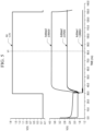
- FIGURE 5 illustrates a timing diagram of output signals of pump circuit 200, according to embodiments of the present disclosure.
- outputs of pump circuit 200 may be stable within approximately 10 ms.
- the outputs include V1, V2, V3 denoted by the /lcdbias1, /lcdbias2, and /lcdbias3 traces.
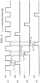
- FIGURE 6 illustrates a timing diagram of output of clock generator circuit 104 in a 3-phase mode, according to embodiments of the present disclosure. This mode may be used to implement 5V outputs to displays with full current.
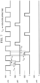
- FIGURE 7 illustrates a timing diagram of output of clock generator circuit 104 in a 2-phase mode, according to embodiments of the present disclosure. This mode may be used to implement 3V outputs to displays with full current or 5V outputs to displays with reduced current.
- FIGURE 8 illustrates a timing diagram of output of clock generator circuit 104 in a 1-phase mode, according to embodiments of the present disclosure. This mode may be used to implement 3V outputs to displays with reduced current.
- clock generator circuit 104 is shown as generated non-overlapping clock signals with a specific phase and frequency relationship between the signals. Specifically, when phic is high, none of phi 1, phi2, or phi3 are high. One of phi 1, phi2, and phi3 is high during a time when phic is low. Phic, phi1, phi2, and phi3 do not overlap. Accordingly, as shown in FIGURE 2 , only switches associated with one of phic, phi1, phi2, and phi3 are switched on at any given moment in time. In each period of phic, when phic is low, one of phi1, phi2, and phi3 might be switched on in a non-overlapping manner.
- phi1, phi2, and phi3 may depend upon whether clock generator circuit 104 is generating a 1-phase, 2-phase, or 3-phase signal.
- clock generator circuit 104 is generating a 3-phase signal
- phi1, phi2, and phi3 are switched on in alternating fashion during parts of the phic period when phic is low, as shown in FIGURE 6 .
- clock generator circuit 104 is generating a 2-phase signal
- phi1 and phi2 are switched on in alternating fashion during parts of the phic period when phic is low, as shown in FIGURE 7 .
- Clock generator circuit 104 When clock generator circuit 104 is generating a 1-phase signal, phi1 are switched on fashion during parts of the phic period when phic is low, as shown in FIGURE 8 .
- Clock generator circuit 104 may be implemented in any suitable manner to generate the signals of FIGURES 6-8 according to the specified mode.
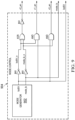
- FIGURE 9 is a more detailed illustration of mode control circuit 102, according to embodiments of the present disclosure.
- Mode control circuit 102 may include a mode generator circuit 902.
- Mode generator circuit 902 may be configured to directly access the register, jumper, memory, data line, or other input from the rest of system 100 identifying which mode is to be used.
- Mode generator circuit 902 may issue lcd5V and mode_lc to the rest of system 100 and to digital logic 904.
- Digital logic 904 may include sufficient elements to interpret the combination of lcd5V and mode_lc into V1_en, V2_en, and V3_en signals.
- Example logic is shown in FIGURE 9 . These enable signals may be defined according to the values in FIGURE 3 .
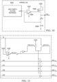
- FIGURE 10 is a more detailed illustration of LDO 106, according to embodiments of the present disclosure.
- LDO 106 may include a voltage reference from system 100, such as a zero-temperature coefficient voltage reference 1002 generating a vref. This may be passed into an op-amp 1004, powered by the Avdd signal and receiving a feedback signal from a resistor network 1008 connected to the output of op-amp 1004. The output of op-amp 1004 may be sent out as Vreg and to the bottom of a transistor 1006 configured as a voltage driver and a top of resistor network 1008.
- One or more resistors of resistor network 1008 may be variable, allowing LDO 106 to be a variable output LDO with different set values. This may be used, for example, to set the LDO output so as to eventually power a 3V or a 5V display.
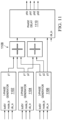
- FIGURE 11 is a more detailed illustration of clock generation circuit 104, according to embodiments of the present disclosure.
- Clock generator circuit 104 may be configured to generate the timing signals for phic, phi1, phi2, and phi3 according to one of FIGURES 6-8 , depending upon input signals lcd5V and mode_lc. These timing signals may be based upon the input clock.
- Clock generator circuit 104 may include any suitable number of signal generators 1102, 1104, 1106. These signal generators may be configured to generate possible constituents of the phased signals. The output may be combined using summer circuits 1108 and a phase delay circuit 1110 may ensure that the output signals are non-overlapping.
- FIGURE 12 is a more detailed illustration of bootstrap circuit 108, according to embodiments of the present disclosure.
- Each of phic, phi1, phi2, and phi3 may be boosted by either the V3 output of the pump or an Avdd voltage value, depending upon which one is greater.
- Avdd voltage value is set by greater system or user requirements, where a system is typically a microcontroller or similar system.
- a comparator in bootstrap circuit 108 compares the Avdd against the V3 signal. If Avdd is greater than the V3 signal, then Avdd is added to buffers for phic/phi 1/phi2/phi3, and each of phic/phi1/phi2/phi3 is shifted up by Avdd.
- V3 is switched into the buffers for phic/phi1/phi2/phi3, and each of phic/phi1/phi2/phi3 is shifted up by V3.
- the output for phic/phi1/phi2/phi3 is thus denoted with a "_u", denoting a shift up in value as needed.
- the switches and circuitry shown in FIGURE 12 represent an example implementation of this functionality.
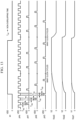
- FIGURE 13 is a timing diagram illustrating operation of the system, according to embodiments of the present disclosure.
- Example signals for an enable, phic, phi1, phi2, phi3, and resulting intermediate signals VLCD1, VLCD2, and VLCD3 are shown.
- Non-overlapping time is denoted as "Tno”.
Landscapes
- Engineering & Computer Science (AREA)
- Physics & Mathematics (AREA)
- Theoretical Computer Science (AREA)
- Computer Hardware Design (AREA)
- General Physics & Mathematics (AREA)
- Crystallography & Structural Chemistry (AREA)
- Chemical & Material Sciences (AREA)
- General Engineering & Computer Science (AREA)
- Software Systems (AREA)
- Mathematical Physics (AREA)
- Computing Systems (AREA)
- Power Engineering (AREA)
- Dc-Dc Converters (AREA)
- Liquid Crystal Display Device Control (AREA)
- Control Of Indicators Other Than Cathode Ray Tubes (AREA)
- Liquid Crystal (AREA)
Description
- The present disclosure relates to liquid crystal display (LCD) bias voltage generators and, in particular, generators suitable for microcontroller integration.
- Microcontrollers are systems on a chip that comprise a microprocessor, memory, and a plurality of integrated peripheral devices. A wide variety of microcontrollers such as 8-bit, 16-bit, and 32-bit microcontrollers are available. Many microcontrollers comprise integrated liquid crystal display (LCD) interfaces that are capable of driving a wide variety of displays. Thus, no external controllers are necessary to interface with such displays.
- US Patent Application Publication
US 2010/328286 discloses an LCD controller with oscillator prebias control. To be able to directly drive an LCD display, such an integrated peripheral needs a voltage bias generator suitable to generate the bias voltage needed to operate the LCD. LCD bias generators are mainly targeted for 3V LCD panels, while there arelegacy 5V LCD panels still in use. Microcontrollers that support both 3V and 5V LCD panels utilize two separate pumps. - Therefore, it is an object of the present application to provide a bias generator that is capable of generating suitable sets of bias voltages for different types of LCDs having different supply voltage requirements, such as 3V LCDs and 5V LCDs. This and other objects can be achieved by a bias generator circuit, microcontroller and method as defined in the independent claims. Further enhancements are characterized in the dependent claims.
- For better understanding and illustration of the present disclosure, the following drawings are included.
-
FIGURE 1 is an illustration of an example embodiment of a system capable of providing power to or driving two or more different kinds of displays or other electronic devices that are powered using a pump source, according to embodiments of the present disclosure. -
FIGURE 2 illustrates an example embodiment of a pump circuit, according to embodiments of the present disclosure. -
FIGURES 3 and 4 illustrate operation of a pump circuit and associated system with respect to various modes of operation, according to embodiments of the present disclosure. -
FIGURE 5 illustrates a timing diagram of output signals of a pump circuit, according to embodiments of the present disclosure. -
FIGURE 6 illustrates a timing diagram of output of a clock generator circuit in a 3-phase mode, according to embodiments of the present disclosure. -
FIGURE 7 illustrates a timing diagram of output of a clock generator circuit in a 2-phase mode, according to embodiments of the present disclosure. -
FIGURE 8 illustrates a timing diagram of output of a clock generator circuit in a 1-phase mode, according to embodiments of the present disclosure. -
FIGURE 9 is a more detailed illustration of a mode control circuit, according to embodiments of the present disclosure. -
FIGURE 10 is a more detailed illustration of a voltage regulator, according to embodiments of the present disclosure. -
FIGURE 11 is a more detailed illustration of a clock generation circuit, according to embodiments of the present disclosure. -
FIGURE 12 is a more detailed illustration of a bootstrap circuit, according to embodiments of the present disclosure. -
FIGURE 13 is a timing diagram illustrating operation of the system, according to embodiments of the present disclosure. - Embodiments of the present disclosure include a bias voltage generator circuit. The bias voltage generator circuit includes a mode control circuit, a clock generator circuit coupled with the mode control unit and configured to generate a plurality of clock signals, and a charge pump circuit configured to receive the clock signals. The charge pump circuit is coupled with the mode control circuit and operable to output selectable output voltages according to input from the mode control circuit. The output selectable voltages may depend upon the clock signals.
- In combination with any of the above embodiments, the bias voltage generator circuit may further include a bootstrap circuit coupled between the clock generator circuit and the charge pump circuit.
- In combination with any of the above embodiments, the mode control circuit may be configured to select between a plurality of operating modes defining output of the charge pump circuit.
- In combination with any of the above embodiments, a first operating mode may be configured to provide for a bias voltage for a 3V LCD and a second operating mode is configured to provide for a bias voltage for a 5V LCD.
- In combination with any of the above embodiments, a first operating mode may be configured to provide for a bias voltage with a first current for an LCD and a second operating mode is configured to provide the bias voltage with a second current for the LCD.
- In combination with any of the above embodiments, the clock signals may include non-overlapping pulses of a base signal and a plurality of phased signals, the phased signals selected according to specified output of the charge pump circuit.
- In combination with any of the above embodiments, the clock signals may include non-overlapping pulses of a base signal and one or more phased signals, and the charge pump circuit is configured to output bias voltages based upon the presence of alternating ones of the phased signals.
- In combination with any of the above embodiments, the clock signals include non-overlapping pulses of a base signal and one or more phased signals, the charge pump circuit may be configured to output a first voltage based upon the presence of a first number of different phased signals, the charge pump circuit may be configured to output a second voltage based upon the presence of a second number of different phased signals, the second voltage may be higher than the first voltage, and the second number of different phased signals may be greater than the first number of different phased signals.
- In combination with any of the above embodiments, the clock signals may include non-overlapping pulses of a base signal and one or more phased signals, and the charge pump circuit may be configured to output a voltage based on a number of different phased signals.
- In combination with any of the above embodiments, the clock signals may include non-overlapping pulses of a base signal and one or more phased signals, and the charge pump circuit may be configured to output a bias voltage with a current, the current based upon a number of different phased signals.
- Embodiments of the present disclosure may include a microcontroller with a bias voltage generator circuit and an output routing circuit configured to route output from the bias voltage generator circuit to a display, wherein the bias voltage generator circuit is implemented by any of the embodiments described above.
-
FIGURE 1 is an illustration of an example embodiment of asystem 100 capable of providing power to or driving two or more different kinds of displays or other electronic devices that are powered using a pump source.System 100 may include a voltage or current pump source to power the two or more different kinds of displays. In one embodiment, the ability to power two or more different kinds of displays may represent corresponding modes of a pump insystem 100. In another embodiment,system 100 may be configured to provide power through its pump at different voltages, wherein different displays require different voltage levels, and different voltages are provided in different modes. In yet another embodiment,system 100 may be configured to provide a given voltage at different current levels to a given display, wherein different current levels at the given voltage are provided in different modes. In another embodiment,system 100 may be self-regulating. -
System 100, through its pumps, may provide any suitable voltage to a display or other peripheral device. The voltages may include bias voltages. In one embodiment,system 100 may be configured to provide voltage to power a liquid crystal display (LCD). In another embodiment,system 100 may be configured to provide power to two or more different kinds of LCDs. In a further embodiment,system 100 may be configured to provide power to two or more different kinds of displays through a single pump. In another, further embodiment,system 100 may be configured to provide power to two or more different kinds of displays through a single pump by providing multiple voltage levels and multiple current levels at a given voltage through the single pump. In one embodiment,system 100 may be configured to be able to switch between providing power to the different kinds of display. In a further embodiment,system 100 may be configured to switch between providing power to different kinds of display in response to commands, settings, or other input from a further system in whichsystem 100 is implemented, such as commands or control from a microcontroller. - Other approaches to providing voltages to multiple types of displays, in contrast, may utilize two separate pumps for supporting display panels with different voltages. Using two separate pumps may occupy a large die area on a semiconductor device. Hence,
system 100 may provide an improved bias voltage generator. -
System 100 may be included in any suitable further system, such as a microcontroller, integrated device, system-on-chip, mobile device, etc.System 100 may be implemented in any suitable combination of analog or digital circuitry. Althoughsystem 100 is illustrated with example elements,system 100 may include more or fewer elements. Furthermore, some elements ofsystem 100 may be combined with one another. Also, the functionality of some elements ofsystem 100 may be performed by other elements ofsystem 100 as a variation of the examples presented herein. -
System 100 may include apump 110.Pump 110 may be implemented through any suitable combination of analog and digital circuitry.Pump 110 may be configured to selectively generate bias voltages for multiple different types of displays. Furthermore,pump 110 may be configured to generate a given voltage at different current levels. The variations of different outputs ofpump 110 may be manifested in different modes of operation ofpump 110. Pump 110 may output three different voltage lines that embody the bias voltages that are to be applied to a display-V1, V2, and V3. These may be routed to multiple displays. V1, V2, and V3 may be routed to a specified display using, for example, multiplexers, switches, switch fabric, or other mechanisms, which are not shown. - Pump 110 may determine what bias voltages and currents are to be generated based upon phases of input signals. Furthermore, pump 110 may determine what bias voltages and currents are to be generated based upon enable signals. The phases of input signals and the enable signals may be in turn created by circuitry in
system 100 based upon commands or inputs tosystem 100. In the example ofFIGURE 1 , pump 110 may receive phased input signals phic (phi common), phi1, phi2, and phi3. Furthermore, pump 110 may receive enable signals for V1, V2, and V3, enumerated as V1_en, V2_en, and V3_en. - In the example of
FIGURE 1 , pump 110 is be configured to provide bias voltages to two different kinds of LCD display panels. First, pump 110 is configured to generate bias voltages for 5V LCD display panels. Second, pump 110 is configured to generate bias voltages for 3V LCD display panels. Furthermore, pump 110 is configured to generate the bias voltage for the 5V LCD and 3V LCD display panel at a reduced current level. -
System 100 includes amode control circuit 102 configured to determine what mode operation that pump 110 will operate.Mode control circuit 102 may be implemented by any suitable combination of circuitry, and is discussed in more detail below.Mode control circuit 102 determines what mode of operation that pump 110 will operate in any suitable manner. For example,mode control circuit 102 may receive a command from a microcontroller, read a register value, identify a jumper setting, receive a digital switch value, user configured circuitry, programmable fuse, memory value, register file, or any other mechanism defining the mode to be used. Based upon the mode identified bymode control circuit 102,mode control circuit 102 may issue a first signal identifying whether, for example, 3V or 5V displays are to be powered. For example,mode control circuit 102 may issue a value on a line denoted lcd5V, wherein a low or 0 value represents a 3V mode and a high or 1 value represents a 5V mode. Furthermore, based upon the mode identified bymode control circuit 102,mode control circuit 102 may issue a first signal identifying whether, for example, a low current mode is to be used in the bias voltage for the display. For example,mode control circuit 102 may issue a value on a line denoted mode_lc, wherein a high or 1 value represents a low current mode and a low or 0 value represents a normal current mode. In addition, depending upon the mode selected,mode control circuit 102 may be configured to issue V1_en, V2_en, and V3_en to pump 110. - V1_en, V2_en, and V3_en are control signals that inform
pump 110 whethersystem 100 is to operate in 5V mode, 3V mode, or high or low current mode. Referring toFigure 3 ,3V mode pump 110 assigns Vlcd2, Vlcd1, and Vin to V3, V2, and V1, respectively. In5V mode pump 110 assigns Vlcd3, Vlcd2, and Vlcd1 to V3, V2, and V1, respectively. In 3Vmode LC pump 110 assigns Vlcd3, Vin, and Vin to V3, V2, and V1, respectively. Finally, in5V mode pump 110 assigns Vlcd3, Vlcd2, and Vin to V3, V2, and V1, respectively. Wheneverpump 110 assigns Vin to outputs V3, V2, and V1, it connectsLDO 106 output to outputs V3, V2, and V1. Chold caps 220, 222, 224 are required for operation ofpump 110, where they act as charge reservoirs forpump 110 to supply instantaneous and dynamic currents of an LCD display. Whenpump 110 assigns Vin toV1 Chold 224 can be removed. Assignment of Vin to V2 allows removal ofChold 222.Chold capacitors - Returning to
FIGURE 1 ,system 100 includes aclock generation circuit 104 configured to generate phased signals as inputs to pump 110. The phased signals are the basis forpump 110 generating bias voltages for a selected one of the 3V and 5V display.Clock generation circuit 104 may accept as input a system clock signal.Clock generation circuit 104 is configured to generate phic, phi1, phi2, and phi3 signals.Clock generation circuit 104 is configured to determine the contents of phic, phi1, phi2, and phi3 signals based upon input frommode control circuit 102. The phic, phi1, phi2, and phi3 signals may be routed for additional signal conditioning before being applied to pump 110.Clock generation circuit 104 may be implemented in any suitable combination of circuitry, and is discussed in more detail below. The contents of the phic, phi1, phi2, and phi3 signals are also discussed in more detail below.Clock generation circuit 104 may transform its external clock input into the phic signal and one or more of phi1, phi2, and phi3. Phic signal may always be generated and used bypump 110. Generation of specific ones of phi1, phi2, and phi3, and the use thereof bypump 110, may depend upon the selected mode of operation. Phi1, phi2, and phi3 may each have different phases and periods than each other and phic. Phi1, phi2, and phi3 might each be used or discarded depending upon the mode. -
System 100 may include abootstrap circuit 108.Bootstrap circuit 108 may be configured to ensure that voltage levels of phic, phi1, phi2, and phi3 signals as received atpump 110 are at expected levels or ranges of levels. Pump 110 may be configured to perform as a buck-boost element, and thus always output a constant level (such as, for example, 3V or 5V) even when the system degrades. Thus, if the system degrades, pump 110 may compensate and continue to output at a constant level of 3V or 5V. In order to assistpump 110 in compensating, if necessary,bootstrap circuit 108 may help ensure thatpump 110 receives consistent input with respect to the expected levels of phic, phi1, phi2, and phi3 signals.Bootstrap circuit 108 may output phic_u, phi1_u, phi2_u, and phi3_u signals, designated as boosted or up-conditioned (if necessary) versions of phic, phi1, phi2, and phi3 signals. These may be input to pump 110.Bootstrap circuit 108 may include a system voltage input Avdd. In one embodiment, an output V3 ofpump 110 may be routed to bootstrapcircuit 108 as an input.Bootstrap circuit 108 may use the V3 value, an output ofpump 110, to determine whether to adjust the phased signals forpump 110.Bootstrap circuit 108 may be implemented in any suitable combination of circuitry and is discussed in more detail below. -
System 100 may include a voltage regulator to provide a constant reference voltage to pump 110. For example,system 100 may include a variable low dropout (LDO) voltage regulator, such asLDO 106.LDO 106 may be configured to output a constant reference voltage to pump 110. In one embodiment,LDO 106 may receive V3 frompump 110 as a feedback input. In another embodiment,LDO 106 may be a variable LDO as it calibrates the output to the pump according to voltage bias needs. For example, as output ofpump 110 varies from a desired 3V output,LDO 106 may be configured to adjust the reference voltage to bring the output ofpump 110 back to the desired 3V output.LDO 106 may receive its own power supply from a chip on whichsystem 100 resides.LDO 106 may be implemented in any suitable combination of analog and digital circuitry. - The gain of
pump 110 is controlled by the number of clock phases received through phi1, phi2, and phi3, which are evaluated in view of phic. The output ofpump 110 may be reordered according to the inputs frommode control circuit 102.LDO 106 may dial-in and calibrate output ofpump 110. The levels of clock phases phic, phi1, phi2, and phi3 may be monitored and adjusted or normalized as necessary bybootstrap circuit 108. -
FIGURE 2 illustrates an example embodiment of apump circuit 200, according to embodiments of the present disclosure.Pump circuit 200 may fully or in part implementpump 110.Pump circuit 200 includes a plurality ofswitches Pump circuit 200 includes a fly capacitor,Cfly 214. Intermediate signals inpump circuit 200 include those designated inFIGURE 2 as VLCD3, VLCD2, and VLCD1, Vinp. Each of these VLCD3, VLCD2, and VLCD1, and Vinp intermediate signals are connected to each ofmultiplexers multiplexers pump 110. The enable signals select which of VLCD3, VLCD2, VLCD1, and Vinp will be routed as the V3, V2, and V1 outputs. The V3, V2, and V1 outputs are each made across ahold capacitor - Operation of
pump circuit 200 is illustrated through timing diagrams, described in more detail below.Pump circuit 200 is configured to, through timing and phases of phic, phi1, phi2, and phi3, to pump up voltage from Vinp (received from the LDO) to an appropriate level expected by a given display. The level to which voltage is pumped is determined through the enable signals received atpump circuit 200. Moreover, the voltage levels are multiples of the input voltage. -
Pump circuit 200 operates on the principle of the conservation of charge as different phases of phic, phi1, phi2, and phi3 are applied through their respective circuits toCfly 214. At an initial point, phic is applied acrossCfly 214.Cfly 214 is then initialized or charged to the output of the LDO, such as 1.2V. Thus, the top charge ofCfly 214 is 1.2V while the bottom is 0.0V. Next, if phi1 goes high, the top charge ofCfly 214 may be 2.4V and the bottom may be 1.2V. Thus, the voltage may be bumped or pumped. This is performed while phic is off. Depending upon the mode, this may be repeated until the interim signal voltages VLCD3, etc. are one of 4.8, 3.6, 2.4, and 1.2 V. Depending upon the mode, these are output to the hold capacitors. The bottom hold capacitor might be unnecessary for 3V mode. -
FIGURES 3 and 4 illustrate operation ofpump circuit 200 andsystem 100 with respect to various modes of operation, according to embodiments of the present disclosure. Control signals and resulting output voltages and currents are shown therein. Entries inFIGURE 3 denoted as "VIN" indicate an output wherein a capacitor need not be used when connecting voltage outputs to a panel as such a capacitor is not needed for storage to properly regulate the output signal in such a particular situation. In such situations, the capacitor that need not be used (such as one ofCholds -
FIGURE 5 illustrates a timing diagram of output signals ofpump circuit 200, according to embodiments of the present disclosure. Once a particular mode, such as a 3V mode, has been enabled (denoted by the /en trace), outputs ofpump circuit 200 may be stable within approximately 10 ms. The outputs include V1, V2, V3 denoted by the /lcdbias1, /lcdbias2, and /lcdbias3 traces. -
FIGURE 6 illustrates a timing diagram of output ofclock generator circuit 104 in a 3-phase mode, according to embodiments of the present disclosure. This mode may be used to implement 5V outputs to displays with full current. -
FIGURE 7 illustrates a timing diagram of output ofclock generator circuit 104 in a 2-phase mode, according to embodiments of the present disclosure. This mode may be used to implement 3V outputs to displays with full current or 5V outputs to displays with reduced current. -
FIGURE 8 illustrates a timing diagram of output ofclock generator circuit 104 in a 1-phase mode, according to embodiments of the present disclosure. This mode may be used to implement 3V outputs to displays with reduced current. - In
FIGURES 6-8 ,clock generator circuit 104 is shown as generated non-overlapping clock signals with a specific phase and frequency relationship between the signals. Specifically, when phic is high, none ofphi 1, phi2, or phi3 are high. One ofphi 1, phi2, and phi3 is high during a time when phic is low. Phic, phi1, phi2, and phi3 do not overlap. Accordingly, as shown inFIGURE 2 , only switches associated with one of phic, phi1, phi2, and phi3 are switched on at any given moment in time. In each period of phic, when phic is low, one of phi1, phi2, and phi3 might be switched on in a non-overlapping manner. The specific ones of which ofphi 1, phi2, and phi3 that are switched on may depend upon whetherclock generator circuit 104 is generating a 1-phase, 2-phase, or 3-phase signal. Whenclock generator circuit 104 is generating a 3-phase signal, phi1, phi2, and phi3 are switched on in alternating fashion during parts of the phic period when phic is low, as shown inFIGURE 6 . Whenclock generator circuit 104 is generating a 2-phase signal, phi1 and phi2 are switched on in alternating fashion during parts of the phic period when phic is low, as shown inFIGURE 7 . Whenclock generator circuit 104 is generating a 1-phase signal, phi1 are switched on fashion during parts of the phic period when phic is low, as shown inFIGURE 8 .Clock generator circuit 104 may be implemented in any suitable manner to generate the signals ofFIGURES 6-8 according to the specified mode. -
FIGURE 9 is a more detailed illustration ofmode control circuit 102, according to embodiments of the present disclosure.Mode control circuit 102 may include amode generator circuit 902.Mode generator circuit 902 may be configured to directly access the register, jumper, memory, data line, or other input from the rest ofsystem 100 identifying which mode is to be used.Mode generator circuit 902 may issue lcd5V and mode_lc to the rest ofsystem 100 and todigital logic 904.Digital logic 904 may include sufficient elements to interpret the combination of lcd5V and mode_lc into V1_en, V2_en, and V3_en signals. Example logic is shown inFIGURE 9 . These enable signals may be defined according to the values inFIGURE 3 . -
FIGURE 10 is a more detailed illustration ofLDO 106, according to embodiments of the present disclosure.LDO 106 may include a voltage reference fromsystem 100, such as a zero-temperaturecoefficient voltage reference 1002 generating a vref. This may be passed into an op-amp 1004, powered by the Avdd signal and receiving a feedback signal from aresistor network 1008 connected to the output of op-amp 1004. The output of op-amp 1004 may be sent out as Vreg and to the bottom of atransistor 1006 configured as a voltage driver and a top ofresistor network 1008. One or more resistors ofresistor network 1008 may be variable, allowingLDO 106 to be a variable output LDO with different set values. This may be used, for example, to set the LDO output so as to eventually power a 3V or a 5V display. -
FIGURE 11 is a more detailed illustration ofclock generation circuit 104, according to embodiments of the present disclosure.Clock generator circuit 104 may be configured to generate the timing signals for phic, phi1, phi2, and phi3 according to one ofFIGURES 6-8 , depending upon input signals lcd5V and mode_lc. These timing signals may be based upon the input clock.Clock generator circuit 104 may include any suitable number ofsignal generators summer circuits 1108 and aphase delay circuit 1110 may ensure that the output signals are non-overlapping. -
FIGURE 12 is a more detailed illustration ofbootstrap circuit 108, according to embodiments of the present disclosure. Each of phic, phi1, phi2, and phi3 may be boosted by either the V3 output of the pump or an Avdd voltage value, depending upon which one is greater. Avdd voltage value is set by greater system or user requirements, where a system is typically a microcontroller or similar system. A comparator inbootstrap circuit 108 compares the Avdd against the V3 signal. If Avdd is greater than the V3 signal, then Avdd is added to buffers for phic/phi 1/phi2/phi3, and each of phic/phi1/phi2/phi3 is shifted up by Avdd. If Avdd is less than the V3 signal, V3 is switched into the buffers for phic/phi1/phi2/phi3, and each of phic/phi1/phi2/phi3 is shifted up by V3. The output for phic/phi1/phi2/phi3 is thus denoted with a "_u", denoting a shift up in value as needed. The switches and circuitry shown inFIGURE 12 represent an example implementation of this functionality. -
FIGURE 13 is a timing diagram illustrating operation of the system, according to embodiments of the present disclosure. Example signals for an enable, phic, phi1, phi2, phi3, and resulting intermediate signals VLCD1, VLCD2, and VLCD3 are shown. Non-overlapping time is denoted as "Tno".
Claims (12)
- A bias voltage generator circuit for generating bias voltages for liquid crystal displays with different voltage requirements, comprising:a mode control circuit (102) configured to set one of a plurality of operating modes and to generate a plurality of enabling signals (V1_en, V2_en, V3_en);a clock generator circuit (104) coupled with the mode control unit (102) and configured to generate a plurality of clock signals (phic, phi1 ... phi3) according to a selected operating mode, wherein the clock signals (phic, phi1 ... phi3) include non-overlapping pulses of a base signal and at least one or more sequences of phased signals (phi1 ... phi3), wherein at least one base signal pulse (phic) is generated between subsequent phased signal pulses (phi1 ... phi3); anda charge pump circuit(110; 200) receiving an input voltage (Vin) and being configured to receive the plurality of clock signals (phic, phi1 ... phi3), being coupled with the mode control circuit (102) to receive the enabling signals (V1_en, V2_en, V3_en), and operable in at least one operating mode to output three bias voltages (V1, V2, V3) at a first, second and third output terminal respectively according to input from the mode control circuit (102), the voltage levels of the three bias voltages (V1, V2, V3) depending upon the clock signals (phic, phi1 ... phi3) and being the input voltage (Vin) or multiples of the input voltage (Vin), wherein the charge pump (110; 200) comprises:a fly capacitor (214) having a first terminal coupled through a first switch (206) controlled by the base signal (phic) with the input voltage (Vin) and a second terminal coupled through a second switch (204) controlled by the base signal (phic) with ground; anda third switch (202) controlled by a first of the phased signals (phi1) to couple the second terminal of the fly capacitor (214) with the input voltage (Vin);a fourth switch (212) controlled by the first phased signals (phi1), a fifth switch (210) controlled by a second of the phased signals (phi2), and a sixth switch (208) controlled by a third of the phased signals (phi1), each having a first terminal coupled with the first terminal of the fly capacitor (214);a seventh switch (216) controlled by the second phased signal (phi2) coupled between the second terminal of the fly capacitor (214) and a second terminal of the fourth switch (212);an eighth switch (218) controlled by the third phased signal (phi3) coupled between the second terminal of the fly capacitor (214) and a second terminal of the fifth switch (210);wherein the third, seventh and eighth switches (202, 216, 218) are controlled by the first, second and third phased signals (phi 1, phi2, phi3) such that internal voltages (VLCD1, VLCD2, VLCD3) at the second terminals of the fourth, fifth, and sixth switches are multiples of the input voltage (Vinp);a first, second and third multiplexer (226,228,230) controlled by said enabling signals (V1_en, V2_en, V3_en), each having three inputs and one output, wherein the first input of the first multiplexer (226) is coupled with the second terminal of the fourth switch (212), the second input of the first multiplexer (226) is coupled with the second terminal of the fifth switch (210), and the third input of the first multiplexer (226) is coupled with the second terminal of the sixth switch (208), wherein the first input of the second multiplexer (228) is coupled with the input voltage, the second input of the second multiplexer (228) is coupled with the second terminal of the fourth switch (212), and the third input of the second multiplexer (228) is coupled with the second terminal of the fifth switch (210), and wherein the first and second input of the third multiplexer (230) are coupled with the input voltage, and the third input of the third multiplexer (230) is coupled with the second terminal of the fourth switch (212),three capacitors (220, 222, 224) coupled with the output of the first, second and third multiplexers (226, 228, 230) and to the first, second and third output terminal respectively to store a selected bias voltage;wherein the mode control circuit (102) is configured to select between a plurality of operating modes, each operating mode defining different sets of bias voltages (V1, V2, V3) by selecting the respective first, second or third input of the first, second, and third multiplexer (226, 228, 230) and the number of phased clock signals, wherein each set of bias voltages (V1, V2, V3) is associated with a different type of liquid crystal display.
- The bias voltage generator circuit according to Claim 1, further comprising a bootstrap circuit (108) coupled between the clock generator circuit (104) and the charge pump (110).
- The bias voltage generator circuit according to Claim 1 or 2, further comprising a controllable variable voltage regulator providing the input voltage, wherein a first operating mode is configured to control the voltage regulator to generate the input voltage having a first voltage level and to provide for bias voltages for a 3V LCD and a second operating mode is configured to control the voltage regulator to generate the input voltage having a second voltage level to provide for bias voltages for a 5V LCD.
- The bias voltage generator circuit according to Claim 1 or 2, wherein a first operating mode is configured to provide for a bias voltage with a first current for an LCD and a second operating mode is configured to provide the bias voltage with a second current for the LCD.
- The bias voltage generator circuit according to one of the preceding Claims, wherein the phased signals comprise in a first operating mode a first sequence of phased signal pulses (phi1) wherein one base signal pulse (phic) is generated between subsequent phased signal pulses of the first sequence of phased signal pulses (phi1).
- The bias voltage generator circuit according to Claim 5, wherein the phased signals comprise in a second operating mode a first and a second sequence of phased signal pulses (phi1, phi2), wherein one base signal pulse (phic) is generated between subsequent phased signal pulses of the first sequence of phased signal pulses (phi1) and the second sequence of phased signal pulses (phi2).
- The bias voltage generator circuit according to Claim 6, wherein the phased signals comprise in a third operating mode a first, second and a third sequence of phased signal pulses (phi1, phi2), wherein one base signal pulse (phic) is generated between subsequent phased signal pulses of the first, second, and third sequence of phased signal pulses (phi2).
- The bias voltage generator circuit according to one of the Claims 5-7, wherein in the second operating mode, the multiplexers (226, 228, 230) are controlled to select Vin, 2*Vin, and 3*Vin as bias voltages.
- The bias voltage generator circuit according to Claim 8, wherein in the third operating mode, the multiplexers (226, 228, 230) are controlled to select 2*Vin, 3*Vin, and 4*Vin as bias voltages.
- A microcontroller comprising a bias voltage generator circuit according to one of the preceding Claims.
- A method for providing different sets of bias voltages for liquid crystal displays with different voltage requirements with a bias voltage generator circuit according to one of the preceding claims, comprising the steps of:selecting an operating mode and enabling signals (V1_en, V2_en, V3_en);depending on the operating mode, generating one, two or three phased signals (phi1, phi2, phi3);controlling the charge pump with said base signal and said at least one phased signal (phi1, phi2, phi3) to generate the three bias voltages at the outputs of the three multiplexers (226, 228, 230)..
- The method according to Claim 11, further comprising depending on the operating mode, providing an input voltage having a first or second voltage level.
Applications Claiming Priority (3)
| Application Number | Priority Date | Filing Date | Title |
|---|---|---|---|
| US201662349825P | 2016-06-14 | 2016-06-14 | |
| US15/621,786 US10332476B2 (en) | 2016-06-14 | 2017-06-13 | Multi-mode low current dual voltage self-regulated LCD pump system |
| PCT/US2017/037362 WO2017218611A1 (en) | 2016-06-14 | 2017-06-14 | Multi-mode low current dual voltage self-regulated lcd pump system |
Publications (2)
| Publication Number | Publication Date |
|---|---|
| EP3469700A1 EP3469700A1 (en) | 2019-04-17 |
| EP3469700B1 true EP3469700B1 (en) | 2024-04-24 |
Family
ID=60573031
Family Applications (1)
| Application Number | Title | Priority Date | Filing Date |
|---|---|---|---|
| EP17734569.1A Active EP3469700B1 (en) | 2016-06-14 | 2017-06-14 | Multi-mode low current dual voltage self-regulated lcd pump system |
Country Status (5)
| Country | Link |
|---|---|
| US (2) | US10332476B2 (en) |
| EP (1) | EP3469700B1 (en) |
| CN (1) | CN108702087B (en) |
| TW (1) | TW201813266A (en) |
| WO (1) | WO2017218611A1 (en) |
Families Citing this family (1)
| Publication number | Priority date | Publication date | Assignee | Title |
|---|---|---|---|---|
| TWI678692B (en) * | 2018-12-20 | 2019-12-01 | 大陸商北京集創北方科技股份有限公司 | Display panel driving circuit and display device |
Family Cites Families (10)
| Publication number | Priority date | Publication date | Assignee | Title |
|---|---|---|---|---|
| US5397928A (en) | 1992-01-17 | 1995-03-14 | Sipex Corporation | Voltage tripler using a charge pump having a single multiplexed charge transfer capacitor |
| JP3554497B2 (en) * | 1998-12-08 | 2004-08-18 | シャープ株式会社 | Charge pump circuit |
| GB0416881D0 (en) * | 2004-07-29 | 2004-09-01 | Koninkl Philips Electronics Nv | Apparatus comprising a charge pump and LCD driver comprising such an apparatus |
| CN101069339A (en) * | 2004-12-03 | 2007-11-07 | 罗姆股份有限公司 | Power supply device, light emitting device using such power supply device, and electronic device |
| EP2017946A1 (en) * | 2007-07-20 | 2009-01-21 | Stichting IMEC Nederland | Electronic power conversion circuit |
| DE102007061978B4 (en) * | 2007-12-21 | 2013-04-11 | Infineon Technologies Ag | Circuit arrangement for providing a voltage supply for a transistor driver circuit |
| US8913051B2 (en) | 2009-06-30 | 2014-12-16 | Silicon Laboratories Inc. | LCD controller with oscillator prebias control |
| US20100328199A1 (en) * | 2009-06-30 | 2010-12-30 | Silicon Laboratories Inc. | Lcd controller with bypass mode |
| US9729048B2 (en) * | 2014-08-04 | 2017-08-08 | Skyworks Solutions, Inc. | Apparatus and methods for charge pumps for radio frequency systems |
| JP6510288B2 (en) * | 2015-03-30 | 2019-05-08 | ローム株式会社 | Charge pump circuit |
-
2017
- 2017-06-13 US US15/621,786 patent/US10332476B2/en active Active
- 2017-06-14 WO PCT/US2017/037362 patent/WO2017218611A1/en not_active Ceased
- 2017-06-14 TW TW106119766A patent/TW201813266A/en unknown
- 2017-06-14 EP EP17734569.1A patent/EP3469700B1/en active Active
- 2017-06-14 CN CN201780009819.6A patent/CN108702087B/en active Active
-
2019
- 2019-05-10 US US16/408,593 patent/US10643568B2/en active Active
Also Published As
| Publication number | Publication date |
|---|---|
| US20170358271A1 (en) | 2017-12-14 |
| TW201813266A (en) | 2018-04-01 |
| US10643568B2 (en) | 2020-05-05 |
| CN108702087B (en) | 2021-04-02 |
| US10332476B2 (en) | 2019-06-25 |
| US20190266973A1 (en) | 2019-08-29 |
| CN108702087A (en) | 2018-10-23 |
| WO2017218611A1 (en) | 2017-12-21 |
| EP3469700A1 (en) | 2019-04-17 |
Similar Documents
| Publication | Publication Date | Title |
|---|---|---|
| EP2110936B1 (en) | Autonomous control of multiple supply voltage generators for display drivers. | |
| US8723576B2 (en) | Clock generation circuit, processor system using same, and clock frequency control method | |
| JP4397936B2 (en) | Switching power supply device and electronic device using the same | |
| KR101579838B1 (en) | Apparatus and display system using stabilized drive voltage | |
| WO2009076137A1 (en) | Diode connected regulation of charge pumps | |
| US10630171B2 (en) | Output voltage adjustable circuit, voltage adjustment method and display apparatus | |
| TWI581549B (en) | Power output circuit and related control method | |
| US10643568B2 (en) | Multi-mode low current dual voltage self-regulated LCD pump system | |
| JP2014115391A (en) | Integrated circuit device, integrated circuit, panel display device and display panel driver | |
| US10152937B2 (en) | Semiconductor device, power supply circuit, and liquid crystal display device | |
| US20130111231A1 (en) | Control circuit for power supply of memory | |
| US20080100233A1 (en) | Apparatus Comprising a Charge Pump and Lcd Driver Comprising Such an Apparatus | |
| US20020130708A1 (en) | Arrangement for driving display units with an adaptive start sequence | |
| JP2000278937A (en) | Booster circuit and power supply circuit for liquid crystal display device using the same | |
| US8379012B2 (en) | Selector switch for direct connection of switched regulator to voltage inputs | |
| JP3272931B2 (en) | LCD drive circuit | |
| JP2013009535A (en) | Power circuit and display device using the same | |
| EP3321924B1 (en) | Low power lcd driver circuit | |
| US20150154897A1 (en) | Controller and Display Apparatus with Improved Performance and Associated Methods | |
| CN105632431B (en) | Controller and display device with improved performance and associated methods | |
| JPH08272337A (en) | Display control circuit | |
| KR20050103544A (en) | Power supply circuit for liquid crystal display | |
| CN109686322B (en) | Switching circuit and backlight driving circuit | |
| US20140168551A1 (en) | Controller and display apparatus with improved performance and associated methods | |
| JP2007181288A (en) | Power supply circuit and electronic device using the same |
Legal Events
| Date | Code | Title | Description |
|---|---|---|---|
| STAA | Information on the status of an ep patent application or granted ep patent |
Free format text: STATUS: UNKNOWN |
|
| STAA | Information on the status of an ep patent application or granted ep patent |
Free format text: STATUS: THE INTERNATIONAL PUBLICATION HAS BEEN MADE |
|
| PUAI | Public reference made under article 153(3) epc to a published international application that has entered the european phase |
Free format text: ORIGINAL CODE: 0009012 |
|
| STAA | Information on the status of an ep patent application or granted ep patent |
Free format text: STATUS: REQUEST FOR EXAMINATION WAS MADE |
|
| 17P | Request for examination filed |
Effective date: 20190107 |
|
| AK | Designated contracting states |
Kind code of ref document: A1 Designated state(s): AL AT BE BG CH CY CZ DE DK EE ES FI FR GB GR HR HU IE IS IT LI LT LU LV MC MK MT NL NO PL PT RO RS SE SI SK SM TR |
|
| AX | Request for extension of the european patent |
Extension state: BA ME |
|
| DAV | Request for validation of the european patent (deleted) | ||
| DAX | Request for extension of the european patent (deleted) | ||
| STAA | Information on the status of an ep patent application or granted ep patent |
Free format text: STATUS: EXAMINATION IS IN PROGRESS |
|
| 17Q | First examination report despatched |
Effective date: 20200813 |
|
| GRAP | Despatch of communication of intention to grant a patent |
Free format text: ORIGINAL CODE: EPIDOSNIGR1 |
|
| STAA | Information on the status of an ep patent application or granted ep patent |
Free format text: STATUS: GRANT OF PATENT IS INTENDED |
|
| INTG | Intention to grant announced |
Effective date: 20231122 |
|
| GRAS | Grant fee paid |
Free format text: ORIGINAL CODE: EPIDOSNIGR3 |
|
| GRAA | (expected) grant |
Free format text: ORIGINAL CODE: 0009210 |
|
| STAA | Information on the status of an ep patent application or granted ep patent |
Free format text: STATUS: THE PATENT HAS BEEN GRANTED |
|
| AK | Designated contracting states |
Kind code of ref document: B1 Designated state(s): AL AT BE BG CH CY CZ DE DK EE ES FI FR GB GR HR HU IE IS IT LI LT LU LV MC MK MT NL NO PL PT RO RS SE SI SK SM TR |
|
| REG | Reference to a national code |
Ref country code: GB Ref legal event code: FG4D |
|
| REG | Reference to a national code |
Ref country code: CH Ref legal event code: EP |
|
| REG | Reference to a national code |
Ref country code: DE Ref legal event code: R096 Ref document number: 602017081266 Country of ref document: DE |
|
| REG | Reference to a national code |
Ref country code: IE Ref legal event code: FG4D |
|
| REG | Reference to a national code |
Ref country code: LT Ref legal event code: MG9D |
|
| REG | Reference to a national code |
Ref country code: NL Ref legal event code: MP Effective date: 20240424 |
|
| REG | Reference to a national code |
Ref country code: AT Ref legal event code: MK05 Ref document number: 1680692 Country of ref document: AT Kind code of ref document: T Effective date: 20240424 |
|
| PG25 | Lapsed in a contracting state [announced via postgrant information from national office to epo] |
Ref country code: NL Free format text: LAPSE BECAUSE OF FAILURE TO SUBMIT A TRANSLATION OF THE DESCRIPTION OR TO PAY THE FEE WITHIN THE PRESCRIBED TIME-LIMIT Effective date: 20240424 |
|
| PG25 | Lapsed in a contracting state [announced via postgrant information from national office to epo] |
Ref country code: NL Free format text: LAPSE BECAUSE OF FAILURE TO SUBMIT A TRANSLATION OF THE DESCRIPTION OR TO PAY THE FEE WITHIN THE PRESCRIBED TIME-LIMIT Effective date: 20240424 |
|
| PG25 | Lapsed in a contracting state [announced via postgrant information from national office to epo] |
Ref country code: IS Free format text: LAPSE BECAUSE OF FAILURE TO SUBMIT A TRANSLATION OF THE DESCRIPTION OR TO PAY THE FEE WITHIN THE PRESCRIBED TIME-LIMIT Effective date: 20240824 |
|
| PG25 | Lapsed in a contracting state [announced via postgrant information from national office to epo] |
Ref country code: BG Free format text: LAPSE BECAUSE OF FAILURE TO SUBMIT A TRANSLATION OF THE DESCRIPTION OR TO PAY THE FEE WITHIN THE PRESCRIBED TIME-LIMIT Effective date: 20240424 |
|
| PG25 | Lapsed in a contracting state [announced via postgrant information from national office to epo] |
Ref country code: FI Free format text: LAPSE BECAUSE OF FAILURE TO SUBMIT A TRANSLATION OF THE DESCRIPTION OR TO PAY THE FEE WITHIN THE PRESCRIBED TIME-LIMIT Effective date: 20240424 Ref country code: HR Free format text: LAPSE BECAUSE OF FAILURE TO SUBMIT A TRANSLATION OF THE DESCRIPTION OR TO PAY THE FEE WITHIN THE PRESCRIBED TIME-LIMIT Effective date: 20240424 |
|
| PG25 | Lapsed in a contracting state [announced via postgrant information from national office to epo] |
Ref country code: GR Free format text: LAPSE BECAUSE OF FAILURE TO SUBMIT A TRANSLATION OF THE DESCRIPTION OR TO PAY THE FEE WITHIN THE PRESCRIBED TIME-LIMIT Effective date: 20240725 |
|
| PG25 | Lapsed in a contracting state [announced via postgrant information from national office to epo] |
Ref country code: PT Free format text: LAPSE BECAUSE OF FAILURE TO SUBMIT A TRANSLATION OF THE DESCRIPTION OR TO PAY THE FEE WITHIN THE PRESCRIBED TIME-LIMIT Effective date: 20240826 |
|
| PG25 | Lapsed in a contracting state [announced via postgrant information from national office to epo] |
Ref country code: ES Free format text: LAPSE BECAUSE OF FAILURE TO SUBMIT A TRANSLATION OF THE DESCRIPTION OR TO PAY THE FEE WITHIN THE PRESCRIBED TIME-LIMIT Effective date: 20240424 |
|
| PG25 | Lapsed in a contracting state [announced via postgrant information from national office to epo] |
Ref country code: AT Free format text: LAPSE BECAUSE OF FAILURE TO SUBMIT A TRANSLATION OF THE DESCRIPTION OR TO PAY THE FEE WITHIN THE PRESCRIBED TIME-LIMIT Effective date: 20240424 |
|
| PG25 | Lapsed in a contracting state [announced via postgrant information from national office to epo] |
Ref country code: PL Free format text: LAPSE BECAUSE OF FAILURE TO SUBMIT A TRANSLATION OF THE DESCRIPTION OR TO PAY THE FEE WITHIN THE PRESCRIBED TIME-LIMIT Effective date: 20240424 |
|
| PG25 | Lapsed in a contracting state [announced via postgrant information from national office to epo] |
Ref country code: LV Free format text: LAPSE BECAUSE OF FAILURE TO SUBMIT A TRANSLATION OF THE DESCRIPTION OR TO PAY THE FEE WITHIN THE PRESCRIBED TIME-LIMIT Effective date: 20240424 |
|
| PG25 | Lapsed in a contracting state [announced via postgrant information from national office to epo] |
Ref country code: PT Free format text: LAPSE BECAUSE OF FAILURE TO SUBMIT A TRANSLATION OF THE DESCRIPTION OR TO PAY THE FEE WITHIN THE PRESCRIBED TIME-LIMIT Effective date: 20240826 Ref country code: PL Free format text: LAPSE BECAUSE OF FAILURE TO SUBMIT A TRANSLATION OF THE DESCRIPTION OR TO PAY THE FEE WITHIN THE PRESCRIBED TIME-LIMIT Effective date: 20240424 Ref country code: NO Free format text: LAPSE BECAUSE OF FAILURE TO SUBMIT A TRANSLATION OF THE DESCRIPTION OR TO PAY THE FEE WITHIN THE PRESCRIBED TIME-LIMIT Effective date: 20240724 Ref country code: LV Free format text: LAPSE BECAUSE OF FAILURE TO SUBMIT A TRANSLATION OF THE DESCRIPTION OR TO PAY THE FEE WITHIN THE PRESCRIBED TIME-LIMIT Effective date: 20240424 Ref country code: IS Free format text: LAPSE BECAUSE OF FAILURE TO SUBMIT A TRANSLATION OF THE DESCRIPTION OR TO PAY THE FEE WITHIN THE PRESCRIBED TIME-LIMIT Effective date: 20240824 Ref country code: HR Free format text: LAPSE BECAUSE OF FAILURE TO SUBMIT A TRANSLATION OF THE DESCRIPTION OR TO PAY THE FEE WITHIN THE PRESCRIBED TIME-LIMIT Effective date: 20240424 Ref country code: GR Free format text: LAPSE BECAUSE OF FAILURE TO SUBMIT A TRANSLATION OF THE DESCRIPTION OR TO PAY THE FEE WITHIN THE PRESCRIBED TIME-LIMIT Effective date: 20240725 Ref country code: FI Free format text: LAPSE BECAUSE OF FAILURE TO SUBMIT A TRANSLATION OF THE DESCRIPTION OR TO PAY THE FEE WITHIN THE PRESCRIBED TIME-LIMIT Effective date: 20240424 Ref country code: ES Free format text: LAPSE BECAUSE OF FAILURE TO SUBMIT A TRANSLATION OF THE DESCRIPTION OR TO PAY THE FEE WITHIN THE PRESCRIBED TIME-LIMIT Effective date: 20240424 Ref country code: BG Free format text: LAPSE BECAUSE OF FAILURE TO SUBMIT A TRANSLATION OF THE DESCRIPTION OR TO PAY THE FEE WITHIN THE PRESCRIBED TIME-LIMIT Effective date: 20240424 Ref country code: AT Free format text: LAPSE BECAUSE OF FAILURE TO SUBMIT A TRANSLATION OF THE DESCRIPTION OR TO PAY THE FEE WITHIN THE PRESCRIBED TIME-LIMIT Effective date: 20240424 Ref country code: RS Free format text: LAPSE BECAUSE OF FAILURE TO SUBMIT A TRANSLATION OF THE DESCRIPTION OR TO PAY THE FEE WITHIN THE PRESCRIBED TIME-LIMIT Effective date: 20240724 |
|
| PG25 | Lapsed in a contracting state [announced via postgrant information from national office to epo] |
Ref country code: DK Free format text: LAPSE BECAUSE OF FAILURE TO SUBMIT A TRANSLATION OF THE DESCRIPTION OR TO PAY THE FEE WITHIN THE PRESCRIBED TIME-LIMIT Effective date: 20240424 |
|
| PG25 | Lapsed in a contracting state [announced via postgrant information from national office to epo] |
Ref country code: EE Free format text: LAPSE BECAUSE OF FAILURE TO SUBMIT A TRANSLATION OF THE DESCRIPTION OR TO PAY THE FEE WITHIN THE PRESCRIBED TIME-LIMIT Effective date: 20240424 |
|
| PG25 | Lapsed in a contracting state [announced via postgrant information from national office to epo] |
Ref country code: CZ Free format text: LAPSE BECAUSE OF FAILURE TO SUBMIT A TRANSLATION OF THE DESCRIPTION OR TO PAY THE FEE WITHIN THE PRESCRIBED TIME-LIMIT Effective date: 20240424 |
|
| PG25 | Lapsed in a contracting state [announced via postgrant information from national office to epo] |
Ref country code: SK Free format text: LAPSE BECAUSE OF FAILURE TO SUBMIT A TRANSLATION OF THE DESCRIPTION OR TO PAY THE FEE WITHIN THE PRESCRIBED TIME-LIMIT Effective date: 20240424 Ref country code: RO Free format text: LAPSE BECAUSE OF FAILURE TO SUBMIT A TRANSLATION OF THE DESCRIPTION OR TO PAY THE FEE WITHIN THE PRESCRIBED TIME-LIMIT Effective date: 20240424 |
|
| REG | Reference to a national code |
Ref country code: DE Ref legal event code: R097 Ref document number: 602017081266 Country of ref document: DE |
|
| PG25 | Lapsed in a contracting state [announced via postgrant information from national office to epo] |
Ref country code: SM Free format text: LAPSE BECAUSE OF FAILURE TO SUBMIT A TRANSLATION OF THE DESCRIPTION OR TO PAY THE FEE WITHIN THE PRESCRIBED TIME-LIMIT Effective date: 20240424 |
|
| PG25 | Lapsed in a contracting state [announced via postgrant information from national office to epo] |
Ref country code: SM Free format text: LAPSE BECAUSE OF FAILURE TO SUBMIT A TRANSLATION OF THE DESCRIPTION OR TO PAY THE FEE WITHIN THE PRESCRIBED TIME-LIMIT Effective date: 20240424 Ref country code: SK Free format text: LAPSE BECAUSE OF FAILURE TO SUBMIT A TRANSLATION OF THE DESCRIPTION OR TO PAY THE FEE WITHIN THE PRESCRIBED TIME-LIMIT Effective date: 20240424 Ref country code: RO Free format text: LAPSE BECAUSE OF FAILURE TO SUBMIT A TRANSLATION OF THE DESCRIPTION OR TO PAY THE FEE WITHIN THE PRESCRIBED TIME-LIMIT Effective date: 20240424 Ref country code: EE Free format text: LAPSE BECAUSE OF FAILURE TO SUBMIT A TRANSLATION OF THE DESCRIPTION OR TO PAY THE FEE WITHIN THE PRESCRIBED TIME-LIMIT Effective date: 20240424 Ref country code: DK Free format text: LAPSE BECAUSE OF FAILURE TO SUBMIT A TRANSLATION OF THE DESCRIPTION OR TO PAY THE FEE WITHIN THE PRESCRIBED TIME-LIMIT Effective date: 20240424 Ref country code: CZ Free format text: LAPSE BECAUSE OF FAILURE TO SUBMIT A TRANSLATION OF THE DESCRIPTION OR TO PAY THE FEE WITHIN THE PRESCRIBED TIME-LIMIT Effective date: 20240424 Ref country code: MC Free format text: LAPSE BECAUSE OF FAILURE TO SUBMIT A TRANSLATION OF THE DESCRIPTION OR TO PAY THE FEE WITHIN THE PRESCRIBED TIME-LIMIT Effective date: 20240424 |
|
| REG | Reference to a national code |
Ref country code: CH Ref legal event code: PL |
|
| PG25 | Lapsed in a contracting state [announced via postgrant information from national office to epo] |
Ref country code: LU Free format text: LAPSE BECAUSE OF NON-PAYMENT OF DUE FEES Effective date: 20240614 |
|
| PLBE | No opposition filed within time limit |
Free format text: ORIGINAL CODE: 0009261 |
|
| STAA | Information on the status of an ep patent application or granted ep patent |
Free format text: STATUS: NO OPPOSITION FILED WITHIN TIME LIMIT |
|
| GBPC | Gb: european patent ceased through non-payment of renewal fee |
Effective date: 20240724 |
|
| 26N | No opposition filed |
Effective date: 20250127 |
|
| PG25 | Lapsed in a contracting state [announced via postgrant information from national office to epo] |
Ref country code: IE Free format text: LAPSE BECAUSE OF NON-PAYMENT OF DUE FEES Effective date: 20240614 |
|
| PG25 | Lapsed in a contracting state [announced via postgrant information from national office to epo] |
Ref country code: CH Free format text: LAPSE BECAUSE OF NON-PAYMENT OF DUE FEES Effective date: 20240630 Ref country code: SI Free format text: LAPSE BECAUSE OF FAILURE TO SUBMIT A TRANSLATION OF THE DESCRIPTION OR TO PAY THE FEE WITHIN THE PRESCRIBED TIME-LIMIT Effective date: 20240424 Ref country code: BE Free format text: LAPSE BECAUSE OF NON-PAYMENT OF DUE FEES Effective date: 20240630 |
|
| PG25 | Lapsed in a contracting state [announced via postgrant information from national office to epo] |
Ref country code: FR Free format text: LAPSE BECAUSE OF NON-PAYMENT OF DUE FEES Effective date: 20240624 |
|
| PG25 | Lapsed in a contracting state [announced via postgrant information from national office to epo] |
Ref country code: GB Free format text: LAPSE BECAUSE OF NON-PAYMENT OF DUE FEES Effective date: 20240724 |
|
| REG | Reference to a national code |
Ref country code: BE Ref legal event code: MM Effective date: 20240630 |
|
| PG25 | Lapsed in a contracting state [announced via postgrant information from national office to epo] |
Ref country code: SE Free format text: LAPSE BECAUSE OF FAILURE TO SUBMIT A TRANSLATION OF THE DESCRIPTION OR TO PAY THE FEE WITHIN THE PRESCRIBED TIME-LIMIT Effective date: 20240424 |
|
| PG25 | Lapsed in a contracting state [announced via postgrant information from national office to epo] |
Ref country code: CY Free format text: LAPSE BECAUSE OF FAILURE TO SUBMIT A TRANSLATION OF THE DESCRIPTION OR TO PAY THE FEE WITHIN THE PRESCRIBED TIME-LIMIT; INVALID AB INITIO Effective date: 20170614 |
|
| PG25 | Lapsed in a contracting state [announced via postgrant information from national office to epo] |
Ref country code: IT Free format text: LAPSE BECAUSE OF FAILURE TO SUBMIT A TRANSLATION OF THE DESCRIPTION OR TO PAY THE FEE WITHIN THE PRESCRIBED TIME-LIMIT Effective date: 20240424 |
|
| PG25 | Lapsed in a contracting state [announced via postgrant information from national office to epo] |
Ref country code: HU Free format text: LAPSE BECAUSE OF FAILURE TO SUBMIT A TRANSLATION OF THE DESCRIPTION OR TO PAY THE FEE WITHIN THE PRESCRIBED TIME-LIMIT; INVALID AB INITIO Effective date: 20170614 |
|
| PG25 | Lapsed in a contracting state [announced via postgrant information from national office to epo] |
Ref country code: TR Free format text: LAPSE BECAUSE OF FAILURE TO SUBMIT A TRANSLATION OF THE DESCRIPTION OR TO PAY THE FEE WITHIN THE PRESCRIBED TIME-LIMIT Effective date: 20240424 |
|
| PG25 | Lapsed in a contracting state [announced via postgrant information from national office to epo] |
Ref country code: LT Free format text: LAPSE BECAUSE OF FAILURE TO SUBMIT A TRANSLATION OF THE DESCRIPTION OR TO PAY THE FEE WITHIN THE PRESCRIBED TIME-LIMIT Effective date: 20240424 |
|
| PGFP | Annual fee paid to national office [announced via postgrant information from national office to epo] |
Ref country code: DE Payment date: 20260520 Year of fee payment: 10 |